EP4004978B1 - Composant électrique et/ou électronique et agencement de contacts - Google Patents
Composant électrique et/ou électronique et agencement de contacts Download PDFInfo
- Publication number
- EP4004978B1 EP4004978B1 EP20750192.5A EP20750192A EP4004978B1 EP 4004978 B1 EP4004978 B1 EP 4004978B1 EP 20750192 A EP20750192 A EP 20750192A EP 4004978 B1 EP4004978 B1 EP 4004978B1
- Authority
- EP
- European Patent Office
- Prior art keywords
- contact
- connection
- electrical
- electronic component
- connection lug
- Prior art date
- Legal status (The legal status is an assumption and is not a legal conclusion. Google has not performed a legal analysis and makes no representation as to the accuracy of the status listed.)
- Active
Links
- 238000003466 welding Methods 0.000 claims description 60
- 238000005452 bending Methods 0.000 claims description 53
- 239000000758 substrate Substances 0.000 claims description 22
- 238000000034 method Methods 0.000 claims description 21
- 230000015572 biosynthetic process Effects 0.000 description 6
- 239000002184 metal Substances 0.000 description 6
- 229910052751 metal Inorganic materials 0.000 description 6
- RYGMFSIKBFXOCR-UHFFFAOYSA-N Copper Chemical compound [Cu] RYGMFSIKBFXOCR-UHFFFAOYSA-N 0.000 description 5
- 229910052802 copper Inorganic materials 0.000 description 5
- 239000010949 copper Substances 0.000 description 5
- 238000011161 development Methods 0.000 description 3
- 230000018109 developmental process Effects 0.000 description 3
- 239000007769 metal material Substances 0.000 description 3
- 238000004519 manufacturing process Methods 0.000 description 2
- 239000012778 molding material Substances 0.000 description 2
- 238000005219 brazing Methods 0.000 description 1
- 239000000919 ceramic Substances 0.000 description 1
- 230000001419 dependent effect Effects 0.000 description 1
- 239000013071 indirect material Substances 0.000 description 1
- 238000005304 joining Methods 0.000 description 1
- 230000007257 malfunction Effects 0.000 description 1
- 239000000463 material Substances 0.000 description 1
- 238000002360 preparation method Methods 0.000 description 1
- 238000003825 pressing Methods 0.000 description 1
- 230000005855 radiation Effects 0.000 description 1
- 229910000679 solder Inorganic materials 0.000 description 1
- 239000007787 solid Substances 0.000 description 1
Images

Classifications
-
- H—ELECTRICITY
- H01—ELECTRIC ELEMENTS
- H01R—ELECTRICALLY-CONDUCTIVE CONNECTIONS; STRUCTURAL ASSOCIATIONS OF A PLURALITY OF MUTUALLY-INSULATED ELECTRICAL CONNECTING ELEMENTS; COUPLING DEVICES; CURRENT COLLECTORS
- H01R13/00—Details of coupling devices of the kinds covered by groups H01R12/70 or H01R24/00 - H01R33/00
- H01R13/02—Contact members
-
- H—ELECTRICITY
- H01—ELECTRIC ELEMENTS
- H01L—SEMICONDUCTOR DEVICES NOT COVERED BY CLASS H10
- H01L23/00—Details of semiconductor or other solid state devices
- H01L23/48—Arrangements for conducting electric current to or from the solid state body in operation, e.g. leads, terminal arrangements ; Selection of materials therefor
- H01L23/488—Arrangements for conducting electric current to or from the solid state body in operation, e.g. leads, terminal arrangements ; Selection of materials therefor consisting of soldered or bonded constructions
- H01L23/495—Lead-frames or other flat leads
- H01L23/49517—Additional leads
- H01L23/49524—Additional leads the additional leads being a tape carrier or flat leads
-
- H—ELECTRICITY
- H01—ELECTRIC ELEMENTS
- H01L—SEMICONDUCTOR DEVICES NOT COVERED BY CLASS H10
- H01L23/00—Details of semiconductor or other solid state devices
- H01L23/48—Arrangements for conducting electric current to or from the solid state body in operation, e.g. leads, terminal arrangements ; Selection of materials therefor
- H01L23/488—Arrangements for conducting electric current to or from the solid state body in operation, e.g. leads, terminal arrangements ; Selection of materials therefor consisting of soldered or bonded constructions
- H01L23/495—Lead-frames or other flat leads
- H01L23/49517—Additional leads
-
- B—PERFORMING OPERATIONS; TRANSPORTING
- B23—MACHINE TOOLS; METAL-WORKING NOT OTHERWISE PROVIDED FOR
- B23K—SOLDERING OR UNSOLDERING; WELDING; CLADDING OR PLATING BY SOLDERING OR WELDING; CUTTING BY APPLYING HEAT LOCALLY, e.g. FLAME CUTTING; WORKING BY LASER BEAM
- B23K26/00—Working by laser beam, e.g. welding, cutting or boring
- B23K26/20—Bonding
- B23K26/21—Bonding by welding
- B23K26/22—Spot welding
-
- B—PERFORMING OPERATIONS; TRANSPORTING
- B23—MACHINE TOOLS; METAL-WORKING NOT OTHERWISE PROVIDED FOR
- B23K—SOLDERING OR UNSOLDERING; WELDING; CLADDING OR PLATING BY SOLDERING OR WELDING; CUTTING BY APPLYING HEAT LOCALLY, e.g. FLAME CUTTING; WORKING BY LASER BEAM
- B23K26/00—Working by laser beam, e.g. welding, cutting or boring
- B23K26/20—Bonding
- B23K26/21—Bonding by welding
- B23K26/24—Seam welding
- B23K26/244—Overlap seam welding
-
- B—PERFORMING OPERATIONS; TRANSPORTING
- B23—MACHINE TOOLS; METAL-WORKING NOT OTHERWISE PROVIDED FOR
- B23K—SOLDERING OR UNSOLDERING; WELDING; CLADDING OR PLATING BY SOLDERING OR WELDING; CUTTING BY APPLYING HEAT LOCALLY, e.g. FLAME CUTTING; WORKING BY LASER BEAM
- B23K26/00—Working by laser beam, e.g. welding, cutting or boring
- B23K26/20—Bonding
- B23K26/21—Bonding by welding
- B23K26/24—Seam welding
- B23K26/26—Seam welding of rectilinear seams
-
- B—PERFORMING OPERATIONS; TRANSPORTING
- B23—MACHINE TOOLS; METAL-WORKING NOT OTHERWISE PROVIDED FOR
- B23K—SOLDERING OR UNSOLDERING; WELDING; CLADDING OR PLATING BY SOLDERING OR WELDING; CUTTING BY APPLYING HEAT LOCALLY, e.g. FLAME CUTTING; WORKING BY LASER BEAM
- B23K26/00—Working by laser beam, e.g. welding, cutting or boring
- B23K26/20—Bonding
- B23K26/32—Bonding taking account of the properties of the material involved
-
- B—PERFORMING OPERATIONS; TRANSPORTING
- B23—MACHINE TOOLS; METAL-WORKING NOT OTHERWISE PROVIDED FOR
- B23K—SOLDERING OR UNSOLDERING; WELDING; CLADDING OR PLATING BY SOLDERING OR WELDING; CUTTING BY APPLYING HEAT LOCALLY, e.g. FLAME CUTTING; WORKING BY LASER BEAM
- B23K37/00—Auxiliary devices or processes, not specially adapted to a procedure covered by only one of the preceding main groups
- B23K37/04—Auxiliary devices or processes, not specially adapted to a procedure covered by only one of the preceding main groups for holding or positioning work
- B23K37/0426—Fixtures for other work
- B23K37/0435—Clamps
- B23K37/0443—Jigs
-
- H—ELECTRICITY
- H01—ELECTRIC ELEMENTS
- H01L—SEMICONDUCTOR DEVICES NOT COVERED BY CLASS H10
- H01L21/00—Processes or apparatus adapted for the manufacture or treatment of semiconductor or solid state devices or of parts thereof
- H01L21/02—Manufacture or treatment of semiconductor devices or of parts thereof
- H01L21/04—Manufacture or treatment of semiconductor devices or of parts thereof the devices having potential barriers, e.g. a PN junction, depletion layer or carrier concentration layer
- H01L21/48—Manufacture or treatment of parts, e.g. containers, prior to assembly of the devices, using processes not provided for in a single one of the subgroups H01L21/06 - H01L21/326
- H01L21/4814—Conductive parts
- H01L21/4821—Flat leads, e.g. lead frames with or without insulating supports
- H01L21/4825—Connection or disconnection of other leads to or from flat leads, e.g. wires, bumps, other flat leads
-
- H—ELECTRICITY
- H01—ELECTRIC ELEMENTS
- H01R—ELECTRICALLY-CONDUCTIVE CONNECTIONS; STRUCTURAL ASSOCIATIONS OF A PLURALITY OF MUTUALLY-INSULATED ELECTRICAL CONNECTING ELEMENTS; COUPLING DEVICES; CURRENT COLLECTORS
- H01R13/00—Details of coupling devices of the kinds covered by groups H01R12/70 or H01R24/00 - H01R33/00
- H01R13/02—Contact members
- H01R13/22—Contacts for co-operating by abutting
- H01R13/24—Contacts for co-operating by abutting resilient; resiliently-mounted
- H01R13/2442—Contacts for co-operating by abutting resilient; resiliently-mounted with a single cantilevered beam
-
- H—ELECTRICITY
- H01—ELECTRIC ELEMENTS
- H01R—ELECTRICALLY-CONDUCTIVE CONNECTIONS; STRUCTURAL ASSOCIATIONS OF A PLURALITY OF MUTUALLY-INSULATED ELECTRICAL CONNECTING ELEMENTS; COUPLING DEVICES; CURRENT COLLECTORS
- H01R43/00—Apparatus or processes specially adapted for manufacturing, assembling, maintaining, or repairing of line connectors or current collectors or for joining electric conductors
- H01R43/02—Apparatus or processes specially adapted for manufacturing, assembling, maintaining, or repairing of line connectors or current collectors or for joining electric conductors for soldered or welded connections
- H01R43/0221—Laser welding
-
- B—PERFORMING OPERATIONS; TRANSPORTING
- B23—MACHINE TOOLS; METAL-WORKING NOT OTHERWISE PROVIDED FOR
- B23K—SOLDERING OR UNSOLDERING; WELDING; CLADDING OR PLATING BY SOLDERING OR WELDING; CUTTING BY APPLYING HEAT LOCALLY, e.g. FLAME CUTTING; WORKING BY LASER BEAM
- B23K2101/00—Articles made by soldering, welding or cutting
- B23K2101/36—Electric or electronic devices
-
- H—ELECTRICITY
- H01—ELECTRIC ELEMENTS
- H01L—SEMICONDUCTOR DEVICES NOT COVERED BY CLASS H10
- H01L23/00—Details of semiconductor or other solid state devices
- H01L23/28—Encapsulations, e.g. encapsulating layers, coatings, e.g. for protection
- H01L23/31—Encapsulations, e.g. encapsulating layers, coatings, e.g. for protection characterised by the arrangement or shape
- H01L23/3107—Encapsulations, e.g. encapsulating layers, coatings, e.g. for protection characterised by the arrangement or shape the device being completely enclosed
-
- H—ELECTRICITY
- H01—ELECTRIC ELEMENTS
- H01L—SEMICONDUCTOR DEVICES NOT COVERED BY CLASS H10
- H01L23/00—Details of semiconductor or other solid state devices
- H01L23/48—Arrangements for conducting electric current to or from the solid state body in operation, e.g. leads, terminal arrangements ; Selection of materials therefor
- H01L23/488—Arrangements for conducting electric current to or from the solid state body in operation, e.g. leads, terminal arrangements ; Selection of materials therefor consisting of soldered or bonded constructions
- H01L23/495—Lead-frames or other flat leads
- H01L23/49541—Geometry of the lead-frame
- H01L23/49548—Cross section geometry
- H01L23/49551—Cross section geometry characterised by bent parts
- H01L23/49555—Cross section geometry characterised by bent parts the bent parts being the outer leads
-
- H—ELECTRICITY
- H01—ELECTRIC ELEMENTS
- H01R—ELECTRICALLY-CONDUCTIVE CONNECTIONS; STRUCTURAL ASSOCIATIONS OF A PLURALITY OF MUTUALLY-INSULATED ELECTRICAL CONNECTING ELEMENTS; COUPLING DEVICES; CURRENT COLLECTORS
- H01R12/00—Structural associations of a plurality of mutually-insulated electrical connecting elements, specially adapted for printed circuits, e.g. printed circuit boards [PCB], flat or ribbon cables, or like generally planar structures, e.g. terminal strips, terminal blocks; Coupling devices specially adapted for printed circuits, flat or ribbon cables, or like generally planar structures; Terminals specially adapted for contact with, or insertion into, printed circuits, flat or ribbon cables, or like generally planar structures
- H01R12/70—Coupling devices
- H01R12/71—Coupling devices for rigid printing circuits or like structures
- H01R12/712—Coupling devices for rigid printing circuits or like structures co-operating with the surface of the printed circuit or with a coupling device exclusively provided on the surface of the printed circuit
- H01R12/716—Coupling device provided on the PCB
-
- H—ELECTRICITY
- H01—ELECTRIC ELEMENTS
- H01R—ELECTRICALLY-CONDUCTIVE CONNECTIONS; STRUCTURAL ASSOCIATIONS OF A PLURALITY OF MUTUALLY-INSULATED ELECTRICAL CONNECTING ELEMENTS; COUPLING DEVICES; CURRENT COLLECTORS
- H01R13/00—Details of coupling devices of the kinds covered by groups H01R12/70 or H01R24/00 - H01R33/00
- H01R13/02—Contact members
- H01R13/22—Contacts for co-operating by abutting
- H01R13/24—Contacts for co-operating by abutting resilient; resiliently-mounted
- H01R13/2464—Contacts for co-operating by abutting resilient; resiliently-mounted characterized by the contact point
Definitions
- the invention relates to an electrical and/or electronic component, a contact arrangement comprising the electrical and/or electronic component and a method for forming the contact arrangement according to the preamble of the independent claims.
- An ideal zero gap between the welding partners can be achieved technically simply by pressing both welding partners together using a pliers-like device under elastic and/or plastic deformation until they form a gap-free system contact.
- the necessary space for such a device is not always available.
- handling such a device is often difficult because access must be provided from both sides of the welding partners.
- a counter bearing for the welding device is usually required, for which a support surface - for example on the carrier substrate of the electronic circuit - must be provided.
- DE102007006601 discloses the electrical and mechanical connection of a contact arrangement by means of a laser beam.
- the invention is based on the object of forming welding contacts of electrical and/or electronic components within compact circuits with as few gaps as possible.
- the starting point is an electrical and/or electronic component with at least one electrical external connection contact.
- This is designed as a connection lug connected on one side for electrical contact with a contact partner.
- the connection lug has a connection side with a flat connection surface for electrical contact. In the mechanical model, it therefore corresponds to a bending beam clamped on one side.
- the connection lug is preferably made of a sheet metal material, in particular as a stamped sheet or laser sheet, for example made of copper, and contacts an electrical functional area of the component. As an externally contacted external connection contact, this enables the electrical functional area to be integrated, for example within an electronic circuit.
- the exposed end of the connection lug has a bending leg which is bent out of the plane by a compensation angle towards the connection side.
- connection lug is designed to be flexible in such a way that, when a force is applied from the connection side to the free end of the bending leg by a contact partner that is flat at least in this area, the position of the connection surface can be adjusted at least against the compensation angle until the connection surface rests on the flat contact partner without a gap.
- the connection lug is thus flexible with regard to a weld contact to be formed. advantageously prepared in advance as an optimized welding partner.
- connection leg on the connection side against a force applied from this side enables an initial contact of a flat contact partner, for example a connection clip, moved from the connection side relative to the connection lug, in the area of the free end of the connection lug, i.e. the bending leg.
- a gap can first be formed which tapers in a wedge shape to the initial contact point.
- This gap can now be reduced to a gap-free contact by forcing the connection lug to bend by means of a further force application, for example by a further relative movement of the aforementioned welding mask, preferably a straight relative movement. Due to the ongoing bending of the connection lug, the surface position of the connection surface rotates against the compensation angle to the plane of the contact partner until it is flat and thus gap-free.
- the compensation angle provided therefore enables the required position correction of the connecting surface and compensates for misalignments, for example due to assembly and/or manufacturing tolerances. Since only one-sided force application from the connecting side is required, the formation of a welding contact within a very confined electronic circuit is possible without the counter bearing that would otherwise be required.
- the compensation angle has a value in a range of 0.5° to 5°, preferably in a range of 0.5° to 1.5°. It has been shown that in this range, many initial misalignments subject to tolerances can be compensated for by the position correction of the connecting surface, and the production times for forming a gap are freed up. Welding contact can be kept small due to the short paths until the optimal welding position is reached.
- the optimal welding position is preferably achieved by a fully elastic flexibility of the connection lug, but at least alternatively preferably by a partially elastic flexibility of the connection lug. In this way, the impact forces for the position correction of the connecting surface can also be kept small, so that damage during the formation of a welding contact can be ruled out.
- connection lug has a connection leg. One end of this ends in the bending leg via a bending area and at the other end it then includes the one-sided connection of the connection lug within the electrical and/or electronic component.
- the connection lug advantageously has only one bending point, so that the preparation of the connection lug for an optimally formed weld contact can be implemented very cost-effectively.
- the bend can preferably be introduced into an original connection lug made of a flat sheet metal material, so that in particular a connection leg that extends in a straight line remains. It is generally advantageous for the longitudinal extension of the connection leg to be many times shorter than the longitudinal extension of the bending leg, in particular 2 to 20 times shorter, preferably 5 to 10 times shorter. In this way, the flexibility of the connection lug is increasingly achieved more or less solely through the bending leg.
- the bending point then functions almost like a rigid swivel joint. Furthermore, the optimal welding position can be set more precisely.
- this has a solid housing from which the connection lug protrudes, connected on one side.
- the housing is preferably made of a plastic, in particular a molding material.
- the connection lug is preferably enclosed or covered on all sides by the plastic at its connected end.
- connection lug is arranged at a distance from the bottom connection and/or support side. Furthermore, in a plan view of the connection or support side, the connection lug is connected to it on one side within the electrical and/or electronic component, projecting laterally. The bending leg points away from the connection and/or support side. This provides free access to the connection lugs for one-sided application of force from the connection side. In addition, the spacing enables unhindered bending of the connection lug in the direction of the connection or support side.
- a housed electrical and/or electronic component preferably has an exit point of a connection leg of the connection lug from the housing in a connection plane parallel to the connection or support side. Further preferably, the connecting leg lies up to the bending point within this connecting plane, whereas the bending leg is bent in particular perpendicular to a longitudinal extension of the connecting leg from the connecting plane in the direction of the connecting side of the connecting lug.
- the electrical and/or electronic component is designed as a power module, in particular in the form of a molded module.
- connection lug is designed as a power contact.
- the electrical and/or electronic component can also have two, three or more such connection lugs, exclusively or in addition to at least one external connection contact of a different design.
- the invention also leads to a contact arrangement comprising at least one electrical and/or electronic component in at least one of the previously described embodiments, wherein a connecting contact, in particular a gap-free connecting contact, is formed between the connection lug in the region of the connecting surface and a contact partner that is flat at least in the formed connecting region.
- a connecting contact represents a connection that is functionally reliable over its service life, for example to an electronic circuit.
- the connecting contact is in particular designed as a welding contact is formed. When a laser process is used, a laser welding contact is created.
- connection clip which bridges the connection lug and a connection point of the electronic circuit.
- the connection clip is, for example, a stamped sheet metal part, in particular made of copper.
- the connection clip can have one or more bends, for example in order to span an application-related height offset between the connection lug and the connection point of the electronic circuit.
- the connection clip can also have recesses, in particular in the form of longitudinal slots between the connection points. In this way, the connection clip is given sufficient mechanical elasticity to enable alignment of the intended joining surfaces in the connection areas by bending and/or twisting until they are in gap-free contact with the respective welding partner.
- the electronic circuit is designed as a B2 or B6 bridge, in particular as a circuit part of an inverter.
- the contacting partner is designed as a connection clip, wherein an end of the connection clip spaced from the system contact is held stationary before or during method step b).
- This can be done, for example, by means of a holding tool which picks up the said end and fixes it in place.
- stationary fixation is achieved by at least an indirect material or force-locking and/or positive connection to the carrier substrate.
- a further connection contact is formed between the connection clip and a connection point of an electronic circuit, in particular as a welded contact, between the stationary end of the connection clip and the connection contact to be formed or formed with the connection lug.
- the formation of the further connection contact takes place before, after or together with the connection contact between the connection clip and the connection lug.
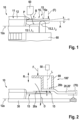
- the Fig.1 shows a side view of an electrical and/or electronic component 10.
- This has an external contact connection 15, which is designed as a connection lug connected on one side.
- the connection is made to a component base body 11, via which the connection lug 15 is contacted with an electrical functional area of the component 10.
- the connection lug 15 is formed, for example, from a sheet metal material, for example from a copper sheet.
- the connection lug 15 has in present embodiment has a bending point B and thus divides the longitudinal extent of the connection lug 15 into at least one longitudinal section I1 of a connection leg 15.1 and an adjoining longitudinal section I2 of a bending leg 15.2.
- connection leg 15.1 is thus connected at one end to the component base body 11 and opens via the other end from the bending point B into one end of the bending leg 15.2.
- the other end of the bending leg 15.2 is exposed.
- the bending leg 15.2 is bent by a compensation angle ⁇ from a connection plane A, in which, for example, a uniform surface side of the still unbent connection lug 15 was arranged before the bend.
- the bending takes place towards a connection side 16 of the connection lug 15.
- the connection side 16 is later used to electrically connect the connection lug 15 as an external connection contact to a contacting partner by means of a connection contact.
- the bending leg 15.2 comprises a connecting surface 16a via which the connecting contact can then be formed.
- the connecting leg 15.1 is preferably arranged with its one surface side in the connection plane A.
- the electrical and/or electronic component 10 also preferably has a housing 12, in particular made of plastic.
- the housing 12 is then formed, for example, from a molding material.
- the electrical and/or electronic component 10 also has a lower connection or support side 12a via which the component 10 can be arranged on a carrier substrate 30.
- the connection lug 15 protrudes from the housing 12 in the area of the connecting leg 15.1 at an exit point P.
- the exit point P is located in particular in the connection plane A, so that the exit point P and the connection plane are arranged at a parallel distance from the lower connection or support side 12a.
- the connection lug 15 is modeled as a bending beam clamped on one side.
- connection side 16a When a force F is applied from the connection side 16a, for example on the exposed end of the bending leg 15.2, a preferably fully elastic or at least partially elastic bending takes place in the direction of the underside connection or support side 12a of the component 10.
- a positional orientation of the connection surface 16a also changes at least against the compensation angle ⁇ .
- the longitudinal section I1 of the connection leg 15.1 is designed to be many times shorter than the longitudinal section I2 of the bending leg 15.2, in particular 2 to 20 times shorter, preferably 5 to 10 times shorter. This results in an increasing rotational movement around the bending point B when the force is applied, which then becomes an essentially rigid swivel joint.
- the bending point B is introduced into a still unbent connecting lug 15 by a bending tool 60, for example.
- the tool 60 comprises, for example, a fixed stop and a movable bending pin, whereby the bending pin bends the connecting lug 15 against the fixed stop in the bending point B towards the connection side 16 by means of a force movement in contact with the latter.
- connection lug In the side view of the Fig.1 only one connection lug is visible in the described embodiment.
- the electrical and/or electronic component 10 can comprise further identical or similar connection lugs 15 exclusively or in addition to at least one external connection contact of a different design.
- the electrical and/or electronic component 10 is prepared for a connection process.
- the carrier substrate 30 is arranged on a carrier substrate 30 via its underside connection or connection side 12a, for example by means of a sintered or solder contact.
- a wide variety of substrate types can be used as the carrier substrate 30, for example a lead frame, a rigid or flexible circuit board, a DBC substrate (double bonded copper), an IMS substrate (insulated metal substrate), an AMB substrate (active metal brazing), an LTCC substrate (low temperature cofired ceramic) or others.
- An initial arrangement 100' is then formed. In this case, a flat area of a support side 20a of a contact partner 20 to be connected is brought into initial contact with the free end of the bending leg 15.2.
- the contact partner 20 can be arranged, for example, by means of an assembly process coming from the connection side 16 of the connection lug 15 in a position in which the support side 20a of the contact point touches the end of the bending leg at an initial contact point E. In this position, the contact partner 20 is held stationary at an end of the contact partner 20 spaced apart from the initial contact point E, for example by a holding tool 70 or by a material or form-fitting and/or force-fitting connection, for example with the Carrier substrate 30.
- a welding mask 80 is placed on a welding side 20b of the contact partner 20 opposite the support side 20a.
- An initial contact can also be formed after the welding mask 80 has been placed on the welding side 20b of a contact partner 20 held stationary on one side and this is moved in the direction of the connection side 16 of the connection lug 15 until the initial contact point E is reached.
- the output arrangement 100' is subjected to a force by a further, for example linear, relative movement R of the welding mask 20 in the direction of the connection side 16 of the connection lug 15. Due to the acting depression force F, the connection lug 15 gives way elastically or at least partially elastically in the direction of the carrier substrate 20 by an at least partial rotational movement D, which also results in a changed position orientation of the connection surface 16a at least opposite to the compensation angle ⁇ of the bending leg 15.2.
- the relative movement R of the welding mask 80 is only held in a welding position in which the connection surface 16a of the connection lug 15 and the support side 20a of the contact partner 20 lie flat against one another.
- a welding contact 40 is then formed as a connection contact using a welding process while maintaining the welding position.
- the welding process is carried out, for example, by means of a laser 50, the laser radiation L of which is directed onto the welding side 20b of the contact partner 20.
- the welding mask 80 is preferably designed in a tube-like manner and in particular has a wall height by which metallic ejections during laser welding are prevented from scattering outside the welding mask 80.
- the formed contact arrangement 100 with the then gap-free welding contact 40 between the connection lug 15 and the contact partner 20 is shown in a side view after removal of the welding mask 80.
- the contact partner 20 is then, for example, a connection clip 20 ⁇ , which is designed in particular as a stamped sheet metal part, preferably made of copper.
- the end of the connecting clip 20' spaced from the welding contact 40 is indirectly connected via a frame element 90 in a force-fitting and/or form-fitting manner to the Carrier substrate 30 and thus held in place, for example via a hole-pin connection.
- a further welding contact 40 is formed as a connecting contact between the connection clip 20' and a connection point 36 of an electronic circuit 35 arranged on the carrier substrate 30.
- the further connecting contact 40 can be formed before, after or together with the connecting contact between the connection clip 20' and the connection lug 15 by means of the laser 50.
- Fig.4 is the contact arrangement from the Fig.3 shown in a perspective view, for example as a circuit part of an inverter 110.
- the electronic circuit 35 comprises a B2 or a B6 bridge, which is formed by at least one described electrical and/or electronic component 10, in particular as a power module, preferably in the form of a mold module.
- two power contacts 15 arranged on the same side are each connected to a connecting clip 20' by means of a gap-free welding contact 40 to form the contact arrangement 100.
Landscapes
- Engineering & Computer Science (AREA)
- Physics & Mathematics (AREA)
- Optics & Photonics (AREA)
- Mechanical Engineering (AREA)
- Plasma & Fusion (AREA)
- Microelectronics & Electronic Packaging (AREA)
- Computer Hardware Design (AREA)
- Power Engineering (AREA)
- Manufacturing & Machinery (AREA)
- General Physics & Mathematics (AREA)
- Condensed Matter Physics & Semiconductors (AREA)
- Coupling Device And Connection With Printed Circuit (AREA)
- Structures For Mounting Electric Components On Printed Circuit Boards (AREA)
Claims (15)
- Composant électrique et/ou électronique (10) ayant au moins un contact de connexion électrique externe (15), qui est conçu sous la forme d'une languette de connexion (15) reliée d'un côté pour la mise en contact électrique avec un partenaire de contact (20, 20'), et la languette de connexion (15) présente, pour le contact électrique, un côté de connexion (16) ayant une surface plate de connexion (16a),
en ce quel'extrémité libre de la languette de connexion (15) présente une branche de flexion (15.2) qui est courbée vers le côté de connexion (16) d'un angle de compensation (α) par rapport au plan (A), la branche de flexion (15.2) qui présente la surface de connexion (16a) et la languette de connexion (15) étant conçue de manière à être flexible, caractériséen ce que, lorsqu'un partenaire de contact plat (20, 20'), soumis à une force provenant du côté de connexion (16), entre en contact avec l'extrémité libre de la branche de flexion (15.2), une orientation de position de la surface de connexion (16a) est apte à être adaptée à l'encontre de l'angle de compensation (α) jusqu'à un appui sans espace de la surface de connexion (16a) sur le partenaire de contact plat (20, 20'). - Composant électrique et/ou électronique (10) selon la revendication 1,
caractérisé en ce que
l'angle de compensation (α) a une valeur comprise entre 0,5° et 5°, de préférence entre 0,5° et 1,5°. - Composant électrique et/ou électronique (10) selon la revendication 1 ou la revendication 2,
caractérisé en ce que
la languette de connexion (15) présente une branche de connexion (15.1), en particulier une branche de connexion droite (15.1), qui débouche par l'une de ses extrémités dans la branche de flexion (15.2) par l'intermédiaire d'un point de flexion (B) et comprend à son autre extrémité une connexion unilatérale de la languette de connexion (15) à l'intérieur du composant électrique et/ou électronique (10). - Composant électrique et/ou électronique (10) selon la revendication 3,
caractérisé en ce que
une extension longitudinale de la branche de connexion (15.1) est plusieurs fois plus courte qu'une extension longitudinale de la branche de flexion (15.2), en particulier de 2 à 20 fois plus courte, de préférence de 5 à 10 fois plus courte. - Composant électrique et/ou électronique (10) selon l'une des revendications précédentes,
caractérisé en ce que
le composant électrique et/ou électronique (10) présente un boîtier (12), d'un côté duquel la languette de connexion (15) fait saillie. - Composant électrique et/ou électronique (10) selon l'une des revendications précédentes,
caractérisé en ce que
le composant électrique et/ou électronique (10) présente un côté de connexion et/ou d'appui (12a) par rapport à un substrat de support (30), la languette de connexion (15) étant agencée à distance du côté de connexion et/ou d'appui (12a) et, dans une vue de dessus du côté de connexion ou d'appui (12a), fait saillie latéralement de celui-ci, à l'intérieur du composant électrique et/ou électronique (10) et est connectée d'un côté, la branche de flexion (15.2) étant orientée à l'opposé du côté de connexion et/ou d'appui (12a). - Composant électrique et/ou électronique (10) selon l'une des revendications précédentes,
caractérisé en ce que
le composant électrique et/ou électronique (10) est conçu sous la forme d'un module de puissance, notamment sous la forme d'un module de moule. - Agencement de contact (100), comprenant au moins un composant électrique et/ou électronique (10) selon l'une des revendications précédentes, dans lequel un contact de connexion (40), en particulier sans espace, est formé entre la languette de connexion (15) au niveau de la surface de connexion (16a) et un partenaire de contact plat (20, 20').
- Agencement de contact (100) selon la revendication 8,
caractérisé en ce que
le contact de connexion (40) est conçu sous la forme d'un contact soudé, en particulier d'un contact soudé au laser. - Agencement de contact (100) selon l'une des revendications 8 ou 9,
caractérisé en ce que
l'agencement de contact (100) est réalisé en tant que partie d'un circuit électronique (35) sur un substrat de support (30), le partenaire de contact (20, 20') étant un clip de connexion qui relie par pontage la languette de connexion (15) et un point de connexion (36) du circuit électronique (35). - Agencement de contact (100) selon la revendication 10,
caractérisé en ce que
le circuit électronique est conçu sous la forme d'un pont B2 ou B6 (120), notamment en tant que partie de circuit d'un inverseur (110). - Procédé de réalisation d'un dispositif de contact (100) selon l'une des revendications 8 à 11, comprenant les étapes suivantes :a) fourniture d'un composant électrique et/ou électronique (10) selon l'une des revendications 1 à 7, par exemple en le disposant sur un substrat support (30) par sa face inférieure de connexion et/ou d'appui (12a),b) réalisation d'un agencement de sortie (100'), en disposant une face d'appui plate (20a) d'un partenaire de contact (20, 20') sur la face de connexion (16) de la languette de connexion (15) en contact d'appui avec l'extrémité exposée de la branche de flexion (15.2) et en posant un masque de soudage (80) sur une face de soudage (20b) opposée à la face d'appui (20a) du partenaire de contact (20, 20'),c) application d'une force sur l'agencement de sortie (100') par une force d'enfoncement (F), en particulier au moyen d'un mouvement relatif (R), de préférence rectiligne, du masque de soudage (80), de telle sorte que, par un fléchissement de la languette de connexion (15) dans la direction de la force, il se produit une orientation de position modifiée de la surface de connexion (16a) à l'encontre de l'angle de compensation (α) de la branche de flexion (15.2),d) maintien d'une position de soudage dans laquelle la surface de connexion (16a) de la languette de connexion (15) et le côté d'appui (20a) du partenaire de contact (20, 20') reposent à plat l'un contre l'autre,e) formation d'un contact soudé (40), par exemple au moyen d'un laser sur la face soudée (20b) du partenaire de contact (20, 20'), en tant que contact de connexion (40) sans espace entre la languette de connexion (15) et le partenaire de contact (20, 20').
- Procédé selon la revendication 12,
caractérisé en ce que
le partenaire de contact (20) est réalisé sous forme de clip de connexion (20'), une extrémité du clip de connexion (20') distante du contact d'appui étant maintenue immobile avant ou pendant l'étape b) du procédé, par exemple au moyen d'un outil de maintien (70) ou d'une liaison au moins indirecte par matière ou par force et/ou par complémentarité de forme avec le substrat de support (30). - Procédé selon la revendication 13,
caractérisé en ce que
entre l'extrémité maintenue fixe du clip de connexion (20') et le contact de connexion (40) à former ou formé avec la languette de connexion (15), un autre contact de connexion (40) est formé entre le clip de connexion (20') et un point de connexion (36) d'un circuit électronique (35), notamment sous forme de contact soudé. - Procédé selon la revendication 14,
caractérisé en ce que
l'autre contact de connexion (40) est formé avant, après ou en même temps que le contact de connexion (40) entre le clip de connexion (20, 20') et la languette de connexion (15).
Applications Claiming Priority (2)
| Application Number | Priority Date | Filing Date | Title |
|---|---|---|---|
| DE102019211077.0A DE102019211077A1 (de) | 2019-07-25 | 2019-07-25 | Elektrisches und/oder elektronisches Bauelement und Kontaktanordnung |
| PCT/EP2020/070758 WO2021013915A1 (fr) | 2019-07-25 | 2020-07-23 | Composant électrique et/ou électronique et agencement de contacts |
Publications (2)
| Publication Number | Publication Date |
|---|---|
| EP4004978A1 EP4004978A1 (fr) | 2022-06-01 |
| EP4004978B1 true EP4004978B1 (fr) | 2024-05-15 |
Family
ID=71899710
Family Applications (1)
| Application Number | Title | Priority Date | Filing Date |
|---|---|---|---|
| EP20750192.5A Active EP4004978B1 (fr) | 2019-07-25 | 2020-07-23 | Composant électrique et/ou électronique et agencement de contacts |
Country Status (5)
| Country | Link |
|---|---|
| US (1) | US20220270956A1 (fr) |
| EP (1) | EP4004978B1 (fr) |
| CN (1) | CN114175406A (fr) |
| DE (1) | DE102019211077A1 (fr) |
| WO (1) | WO2021013915A1 (fr) |
Families Citing this family (1)
| Publication number | Priority date | Publication date | Assignee | Title |
|---|---|---|---|---|
| DE102021120682A1 (de) | 2021-08-09 | 2023-02-09 | Audi Aktiengesellschaft | Verfahren zum Herstellen eines Leistungsmoduls für ein Elektrofahrzeug |
Family Cites Families (3)
| Publication number | Priority date | Publication date | Assignee | Title |
|---|---|---|---|---|
| US6392778B1 (en) * | 1999-03-17 | 2002-05-21 | Koninklijke Philips Electronics N.V. | Opto-electronic element |
| DE102007006601B4 (de) * | 2007-02-09 | 2008-12-04 | Siemens Ag | Anschluss, Verfahren und Vorrichtung zur gleichmäßigen Einkopplung von Laserstrahlen beim Laserschweißen und Laserlöten, insbesondere an hoch reflektierenden Materialien |
| DE102007012501A1 (de) * | 2007-03-15 | 2008-09-18 | Continental Automotive Gmbh | Anordnung aus einem Leitungsträger und einem Schaltungsträger |
-
2019
- 2019-07-25 DE DE102019211077.0A patent/DE102019211077A1/de active Pending
-
2020
- 2020-07-23 CN CN202080053575.3A patent/CN114175406A/zh active Pending
- 2020-07-23 US US17/625,151 patent/US20220270956A1/en active Pending
- 2020-07-23 WO PCT/EP2020/070758 patent/WO2021013915A1/fr active Application Filing
- 2020-07-23 EP EP20750192.5A patent/EP4004978B1/fr active Active
Also Published As
| Publication number | Publication date |
|---|---|
| DE102019211077A1 (de) | 2021-01-28 |
| CN114175406A (zh) | 2022-03-11 |
| WO2021013915A1 (fr) | 2021-01-28 |
| US20220270956A1 (en) | 2022-08-25 |
| EP4004978A1 (fr) | 2022-06-01 |
Similar Documents
| Publication | Publication Date | Title |
|---|---|---|
| DE102006018902B4 (de) | Elektronisches Schaltungsgerät und Verfahren zur Herstellung desselben | |
| EP0712265A1 (fr) | Assemblage électronique | |
| DE102008030101A1 (de) | Lötanschlusselement | |
| DE19912834B4 (de) | Elektronische Steuereinheit | |
| EP4004978B1 (fr) | Composant électrique et/ou électronique et agencement de contacts | |
| DE2414790A1 (de) | Kristall-oszillator | |
| EP3192130B1 (fr) | Procédé de mise en contact électrique par insertion sans soudure de broches électriquement conductrices à insérer dans des cartes de circuits imprimés | |
| EP3794639A1 (fr) | Système de contact, module électronique comportant le système de contact et procédé de création du système de contact | |
| DE102012218433B4 (de) | Kontaktanordnung | |
| EP2609795B1 (fr) | Procédé pour implanter plusieurs composants sur une carte de circuit et circuit électrique comportant une carte de circuit sur laquelle sont implantés plusieurs composants | |
| EP2285197B1 (fr) | Procédé de raccordement d'un composant électrique et d'une plaquette | |
| DE102007006601B4 (de) | Anschluss, Verfahren und Vorrichtung zur gleichmäßigen Einkopplung von Laserstrahlen beim Laserschweißen und Laserlöten, insbesondere an hoch reflektierenden Materialien | |
| DE10129840B4 (de) | Elektrisches Gerät | |
| DE4028105C1 (en) | Coupling plate shaped modules and PCB(s) - establishing electrical contact by row of contacts stamped and bowed out from metal strip | |
| DE10136082A1 (de) | Verfahren zum Vercrimpen und Anschlussklemmencrimpvorrichtung | |
| WO1997008925A1 (fr) | Procede pour etablir une connexion entre au moins deux conducteurs electriques dont l'un est monte sur un substrat de support | |
| BE1029267B1 (de) | Verfahren zur Herstellung einer Kontakteinheit und Kontakteinheit | |
| EP0295446A2 (fr) | Méthode de fabrication d'un contact électrique | |
| DE19840306A1 (de) | Ausrichtleiste | |
| LU500674B1 (de) | Elektrisches Kontaktelement | |
| DE102019125108A1 (de) | Leistungselektronikanordnung umfassend eine Leiterplatte und ein Leistungsmodul, Verfahren zur Herstellung einer Leistungselektronikanordnung, Kraftfahrzeug umfassend eine Leistungselektronikanordnung | |
| DE102021211521A1 (de) | Verfahren zum Ausrichten von Kontaktflächen eines elektrischen und/oder elektronischen Bauelements, insbesondere eines magnetischen Bauelements | |
| DE102019125105A1 (de) | Leistungselektronikanordnung umfassend eine Leiterplatte und ein Leistungsmodul, Kraftfahrzeug umfassend eine Leistungselektronikanordnung, Verfahren zur Herstellung einer Leistungselektronikanordnung | |
| DE102019125106A1 (de) | Leistungselektronikanordnung umfassend eine Leiterplatte und ein Leistungsmodul, Kraftfahrzeug umfassend eine Leistungselektronikanordnung, sowie Verfahren zur Herstellung einer Leistungselektronikanordnung | |
| DE4110686A1 (de) | Kontaktanordnung fuer ein elektrisches oder elektronisches bauteil |
Legal Events
| Date | Code | Title | Description |
|---|---|---|---|
| STAA | Information on the status of an ep patent application or granted ep patent |
Free format text: STATUS: UNKNOWN |
|
| STAA | Information on the status of an ep patent application or granted ep patent |
Free format text: STATUS: THE INTERNATIONAL PUBLICATION HAS BEEN MADE |
|
| PUAI | Public reference made under article 153(3) epc to a published international application that has entered the european phase |
Free format text: ORIGINAL CODE: 0009012 |
|
| STAA | Information on the status of an ep patent application or granted ep patent |
Free format text: STATUS: REQUEST FOR EXAMINATION WAS MADE |
|
| 17P | Request for examination filed |
Effective date: 20220225 |
|
| AK | Designated contracting states |
Kind code of ref document: A1 Designated state(s): AL AT BE BG CH CY CZ DE DK EE ES FI FR GB GR HR HU IE IS IT LI LT LU LV MC MK MT NL NO PL PT RO RS SE SI SK SM TR |
|
| DAV | Request for validation of the european patent (deleted) | ||
| DAX | Request for extension of the european patent (deleted) | ||
| P01 | Opt-out of the competence of the unified patent court (upc) registered |
Effective date: 20230509 |
|
| GRAP | Despatch of communication of intention to grant a patent |
Free format text: ORIGINAL CODE: EPIDOSNIGR1 |
|
| STAA | Information on the status of an ep patent application or granted ep patent |
Free format text: STATUS: GRANT OF PATENT IS INTENDED |
|
| INTG | Intention to grant announced |
Effective date: 20240118 |
|
| GRAS | Grant fee paid |
Free format text: ORIGINAL CODE: EPIDOSNIGR3 |
|
| GRAA | (expected) grant |
Free format text: ORIGINAL CODE: 0009210 |
|
| STAA | Information on the status of an ep patent application or granted ep patent |
Free format text: STATUS: THE PATENT HAS BEEN GRANTED |
|
| AK | Designated contracting states |
Kind code of ref document: B1 Designated state(s): AL AT BE BG CH CY CZ DE DK EE ES FI FR GB GR HR HU IE IS IT LI LT LU LV MC MK MT NL NO PL PT RO RS SE SI SK SM TR |
|
| REG | Reference to a national code |
Ref country code: CH Ref legal event code: EP |