EP3995808A1 - Verfahren zum klassifizieren von unbekannten partikeln auf einer oberfläche einer halbleiterscheibe - Google Patents
Verfahren zum klassifizieren von unbekannten partikeln auf einer oberfläche einer halbleiterscheibe Download PDFInfo
- Publication number
- EP3995808A1 EP3995808A1 EP20206421.8A EP20206421A EP3995808A1 EP 3995808 A1 EP3995808 A1 EP 3995808A1 EP 20206421 A EP20206421 A EP 20206421A EP 3995808 A1 EP3995808 A1 EP 3995808A1
- Authority
- EP
- European Patent Office
- Prior art keywords
- particles
- particle
- size
- chemical composition
- unknown
- Prior art date
- Legal status (The legal status is an assumption and is not a legal conclusion. Google has not performed a legal analysis and makes no representation as to the accuracy of the status listed.)
- Granted
Links
Images
Classifications
-
- G—PHYSICS
- G01—MEASURING; TESTING
- G01N—INVESTIGATING OR ANALYSING MATERIALS BY DETERMINING THEIR CHEMICAL OR PHYSICAL PROPERTIES
- G01N15/00—Investigating characteristics of particles; Investigating permeability, pore-volume or surface-area of porous materials
- G01N15/02—Investigating particle size or size distribution
-
- G—PHYSICS
- G01—MEASURING; TESTING
- G01N—INVESTIGATING OR ANALYSING MATERIALS BY DETERMINING THEIR CHEMICAL OR PHYSICAL PROPERTIES
- G01N15/00—Investigating characteristics of particles; Investigating permeability, pore-volume or surface-area of porous materials
- G01N15/02—Investigating particle size or size distribution
- G01N15/0205—Investigating particle size or size distribution by optical means
- G01N15/0227—Investigating particle size or size distribution by optical means using imaging; using holography
-
- G—PHYSICS
- G01—MEASURING; TESTING
- G01N—INVESTIGATING OR ANALYSING MATERIALS BY DETERMINING THEIR CHEMICAL OR PHYSICAL PROPERTIES
- G01N23/00—Investigating or analysing materials by the use of wave or particle radiation, e.g. X-rays or neutrons, not covered by groups G01N3/00 – G01N17/00, G01N21/00 or G01N22/00
- G01N23/22—Investigating or analysing materials by the use of wave or particle radiation, e.g. X-rays or neutrons, not covered by groups G01N3/00 – G01N17/00, G01N21/00 or G01N22/00 by measuring secondary emission from the material
- G01N23/2206—Combination of two or more measurements, at least one measurement being that of secondary emission, e.g. combination of secondary electron [SE] measurement and back-scattered electron [BSE] measurement
- G01N23/2208—Combination of two or more measurements, at least one measurement being that of secondary emission, e.g. combination of secondary electron [SE] measurement and back-scattered electron [BSE] measurement all measurements being of a secondary emission, e.g. combination of SE measurement and characteristic X-ray measurement
-
- G—PHYSICS
- G01—MEASURING; TESTING
- G01N—INVESTIGATING OR ANALYSING MATERIALS BY DETERMINING THEIR CHEMICAL OR PHYSICAL PROPERTIES
- G01N23/00—Investigating or analysing materials by the use of wave or particle radiation, e.g. X-rays or neutrons, not covered by groups G01N3/00 – G01N17/00, G01N21/00 or G01N22/00
- G01N23/22—Investigating or analysing materials by the use of wave or particle radiation, e.g. X-rays or neutrons, not covered by groups G01N3/00 – G01N17/00, G01N21/00 or G01N22/00 by measuring secondary emission from the material
- G01N23/225—Investigating or analysing materials by the use of wave or particle radiation, e.g. X-rays or neutrons, not covered by groups G01N3/00 – G01N17/00, G01N21/00 or G01N22/00 by measuring secondary emission from the material using electron or ion
- G01N23/2251—Investigating or analysing materials by the use of wave or particle radiation, e.g. X-rays or neutrons, not covered by groups G01N3/00 – G01N17/00, G01N21/00 or G01N22/00 by measuring secondary emission from the material using electron or ion using incident electron beams, e.g. scanning electron microscopy [SEM]
- G01N23/2252—Measuring emitted X-rays, e.g. electron probe microanalysis [EPMA]
-
- G—PHYSICS
- G01—MEASURING; TESTING
- G01N—INVESTIGATING OR ANALYSING MATERIALS BY DETERMINING THEIR CHEMICAL OR PHYSICAL PROPERTIES
- G01N15/00—Investigating characteristics of particles; Investigating permeability, pore-volume or surface-area of porous materials
- G01N2015/0038—Investigating nanoparticles
-
- G—PHYSICS
- G01—MEASURING; TESTING
- G01N—INVESTIGATING OR ANALYSING MATERIALS BY DETERMINING THEIR CHEMICAL OR PHYSICAL PROPERTIES
- G01N15/00—Investigating characteristics of particles; Investigating permeability, pore-volume or surface-area of porous materials
- G01N15/10—Investigating individual particles
- G01N15/14—Optical investigation techniques, e.g. flow cytometry
- G01N2015/1493—Particle size
-
- G—PHYSICS
- G01—MEASURING; TESTING
- G01N—INVESTIGATING OR ANALYSING MATERIALS BY DETERMINING THEIR CHEMICAL OR PHYSICAL PROPERTIES
- G01N2223/00—Investigating materials by wave or particle radiation
- G01N2223/07—Investigating materials by wave or particle radiation secondary emission
- G01N2223/079—Investigating materials by wave or particle radiation secondary emission incident electron beam and measuring excited X-rays
-
- G—PHYSICS
- G01—MEASURING; TESTING
- G01N—INVESTIGATING OR ANALYSING MATERIALS BY DETERMINING THEIR CHEMICAL OR PHYSICAL PROPERTIES
- G01N2223/00—Investigating materials by wave or particle radiation
- G01N2223/10—Different kinds of radiation or particles
- G01N2223/101—Different kinds of radiation or particles electromagnetic radiation
- G01N2223/1016—X-ray
-
- G—PHYSICS
- G01—MEASURING; TESTING
- G01N—INVESTIGATING OR ANALYSING MATERIALS BY DETERMINING THEIR CHEMICAL OR PHYSICAL PROPERTIES
- G01N2223/00—Investigating materials by wave or particle radiation
- G01N2223/10—Different kinds of radiation or particles
- G01N2223/102—Different kinds of radiation or particles beta or electrons
-
- G—PHYSICS
- G01—MEASURING; TESTING
- G01N—INVESTIGATING OR ANALYSING MATERIALS BY DETERMINING THEIR CHEMICAL OR PHYSICAL PROPERTIES
- G01N2223/00—Investigating materials by wave or particle radiation
- G01N2223/30—Accessories, mechanical or electrical features
- G01N2223/303—Accessories, mechanical or electrical features calibrating, standardising
- G01N2223/3037—Accessories, mechanical or electrical features calibrating, standardising standards (constitution)
-
- G—PHYSICS
- G01—MEASURING; TESTING
- G01N—INVESTIGATING OR ANALYSING MATERIALS BY DETERMINING THEIR CHEMICAL OR PHYSICAL PROPERTIES
- G01N2223/00—Investigating materials by wave or particle radiation
- G01N2223/30—Accessories, mechanical or electrical features
- G01N2223/304—Accessories, mechanical or electrical features electric circuits, signal processing
-
- G—PHYSICS
- G01—MEASURING; TESTING
- G01N—INVESTIGATING OR ANALYSING MATERIALS BY DETERMINING THEIR CHEMICAL OR PHYSICAL PROPERTIES
- G01N2223/00—Investigating materials by wave or particle radiation
- G01N2223/40—Imaging
- G01N2223/418—Imaging electron microscope
-
- G—PHYSICS
- G01—MEASURING; TESTING
- G01N—INVESTIGATING OR ANALYSING MATERIALS BY DETERMINING THEIR CHEMICAL OR PHYSICAL PROPERTIES
- G01N2223/00—Investigating materials by wave or particle radiation
- G01N2223/60—Specific applications or type of materials
- G01N2223/611—Specific applications or type of materials patterned objects; electronic devices
- G01N2223/6116—Specific applications or type of materials patterned objects; electronic devices semiconductor wafer
-
- G—PHYSICS
- G01—MEASURING; TESTING
- G01N—INVESTIGATING OR ANALYSING MATERIALS BY DETERMINING THEIR CHEMICAL OR PHYSICAL PROPERTIES
- G01N2223/00—Investigating materials by wave or particle radiation
- G01N2223/60—Specific applications or type of materials
- G01N2223/633—Specific applications or type of materials thickness, density, surface weight (unit area)
-
- G—PHYSICS
- G01—MEASURING; TESTING
- G01N—INVESTIGATING OR ANALYSING MATERIALS BY DETERMINING THEIR CHEMICAL OR PHYSICAL PROPERTIES
- G01N2223/00—Investigating materials by wave or particle radiation
- G01N2223/60—Specific applications or type of materials
- G01N2223/641—Specific applications or type of materials particle sizing
-
- G—PHYSICS
- G01—MEASURING; TESTING
- G01N—INVESTIGATING OR ANALYSING MATERIALS BY DETERMINING THEIR CHEMICAL OR PHYSICAL PROPERTIES
- G01N2223/00—Investigating materials by wave or particle radiation
- G01N2223/60—Specific applications or type of materials
- G01N2223/652—Specific applications or type of materials impurities, foreign matter, trace amounts
Definitions
- the present invention relates to a method for classifying small foreign particles on semiconductor wafers.
- Monocrystalline semiconductor discs also called wafers
- wafers Monocrystalline semiconductor discs
- Semiconductor wafers in particular semiconductor wafers made of silicon, are usually produced by first drawing a monocrystalline rod using what is known as the float zone process (FZ) or the Czochralski process (CZ).
- the rods produced in this way are divided into crystal pieces using suitable saws such as wire saws, inner hole saws or band saws, which are then usually processed into semiconductor wafers in a wire saw or inner hole saw.
- an epi-layer can optionally be applied by means of CVD.
- the semiconductor wafers produced in this way are then made available for the further component process.
- Particles are an important negative quality feature in wafer production due to shrinking design rules in the component process and are relevant for process and cleaning developments.
- the shape, position and chemical composition usually give an indication of the origin of the contaminating particles and thus the potential to reduce their occurrence in improved processes.
- SEM scanning electron microscope
- EDX Electronic dispersive X -Ray, energy-dispersive X-ray spectroscopy
- This type of analysis is very well suited for particles with an extension of more than 200 nm.
- Particles with smaller dimensions are very difficult to classify because information about the structure of the particles is missing or is subject to large errors.
- the particularly interesting size range of particle diameters is between about 15 nm and 200 nm.
- Particles of this size can no longer be classified using the methods available in the prior art.
- This patent also deals with the detection of particles, information about the structure of the particle remains hidden with this method. In addition, it is an indirect method in which only the location of the particle can be measured.
- the problem here is that the smaller the particles to be examined, the smaller the EDX measurement signal that can be evaluated.
- the environmental conditions e.g. the increasing influence of the signal components from the substrate surface or volume
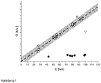
- illustration 1 shows an oxygen measurement value obtained from a spectrum of energy-dispersive X-ray spectroscopy (EDX number of photons in units normalized to 1) as a function of the measured diameter of spherical particles located on a substrate (in this special case a semiconductor wafer made of silicon).
- EDX number of photons in units normalized to 1 EDX number of photons in units normalized to 1
- the data points represented by open circles are values derived from deliberately deposited SiO 2 particles.
- the hatched area reflects the confidence range in which SiO 2 particles should lie with a 95% probability, assuming that the oxygen content for these particles is linearly dependent on the diameter.
- the filled circles are particles that show no significant dependence of the oxygen content on the diameter of the particle.
- the area, in which these particles are located in the figure differ significantly from the previously mentioned confidence range.
- the data point represented by an open triangle is from a particle that appears to show some dependence of oxygen content on its diameter, yet the data point is outside the previously defined confidence range for SiO 2 particles.
- particles of known chemical composition and different sizes are applied to a surface of a substrate (test disc).
- This substrate preferably contains silicon.
- Particles are preferably applied to a test pane with the aid of a suspension in which the particles are present.
- the particles present in the suspension preferably have a very limited size range between 15 nm and 3000 nm. It is also important to ensure that the foreign matter content (unintended contamination) is minimal.
- the particle suspension can be applied analogously to the production of calibration disks for laser scattered light systems.
- the particle suspension can be carried out over the entire area or preferably in partial areas (spots). Using a particle counter can help with this.
- Standard particles with a known size and chemical composition are a good basis for a correct classification of particles.
- Standardized particles with a wide variety of chemical compositions such as aluminum, copper or yttrium are available on the market.
- Particles of the same chemical composition but of different sizes are preferably used, with the size distribution of the particles used being very particularly preferably between 20 nm and 100 nm.
- the size of a number of particles is determined and a spectrum of energy-dispersive X-ray spectroscopy is recorded. Both pieces of information are saved.
- a device from Zeiss, type SEM-EDX, Zeiss - Auriga 60, 70mm 2 - with EDAX Elite Super EDX detector can be used, for example, with the following settings: 5 keV, working distance: 6.1 mm , aperture 30 ⁇ m, EDX integration time: 10 s.
- any other equivalent device can also be used.
- a scanning electron microscope is preferably used to determine the size of the particle of known chemical composition.
- a “size” is understood to mean a determined diameter of the particle; equivalently, a surface of the particle can also be understood, or variables directly derived therefrom can be understood.
- the spectra obtained are preferably evaluated in such a way that they output the substance content of the desired substance. This can be done by evaluating the corresponding peak in the spectrum that is characteristic of the chemical substance.
- SiO 2 particles in which the oxygen content and the size are determined.
- other particles of other known chemical compositions can also be used for the same purpose.
- the substance content is preferably plotted as a function of the size (for example diameter) and a compensation curve is determined from this, which results in a mathematical relationship between substance content and size in the form of a compensation curve.
- Energy-dispersive X-ray spectroscopy is preferably used here.
- the size of the unknown particles is preferably determined using an electron microscope (SEM).
- illustration 1 shows, for example, the oxygen content of SiO 2 particles normalized using energy-dispersive X-ray spectroscopy as a function of the diameter (empty circles).
- a linear regression curve was fitted to show proportionality between oxygen content and diameter.
- a confidence range can also be determined such that 95% of the data points fall within this range.
- Non-SiO 2 particles there is a high probability that an SiO 2 particle can be ruled out as the origin of these particles. These particles would therefore be classified as "non-SiO 2 particles".
- SiO 2 particles For data points that fall within a confidence range for SiO 2 particles, it can be assumed with a high degree of probability that SiO 2 are also particles. The classification is therefore "SiO 2 particles".
- the inventors have recognized that the procedure described is particularly advantageous when it can be assumed that the semiconductor wafer on which the unknown particles are provided with a certain oxide layer, for example a native oxide layer.
- This oxide layer influences energy-dispersive X-ray spectroscopy. Due to the additional information on the size of the particle and the comparison with a compensation curve of known particles, this measurement error shows only a small negative effect.
- Particles with a different chemical composition can also be processed analogously, for example to determine their probable origin.
Landscapes
- Chemical & Material Sciences (AREA)
- General Health & Medical Sciences (AREA)
- Life Sciences & Earth Sciences (AREA)
- Health & Medical Sciences (AREA)
- Analytical Chemistry (AREA)
- Biochemistry (AREA)
- Physics & Mathematics (AREA)
- General Physics & Mathematics (AREA)
- Immunology (AREA)
- Pathology (AREA)
- Dispersion Chemistry (AREA)
- Analysing Materials By The Use Of Radiation (AREA)
- Testing Or Measuring Of Semiconductors Or The Like (AREA)
Abstract
Description
- Die vorliegende Erfindung bezieht sich auf ein Verfahren zur Klassifizierung von kleinen Fremdpartikeln auf Halbleiterscheiben.
- Monokristalline Halbleiterscheiben (auch Wafer genannt) sind die Grundlage der modernen Elektronik. Während der Herstellung von Bauelementen auf besagten Halbleiterscheiben werden thermische Prozesse und mittlerweile recht komplexe Beschichtungsschritte durchgeführt.
- Halbleiterscheiben, insbesondere Halbleiterscheiben aus Silizium, werden üblicherweise hergestellt, indem zuerst ein monokristalliner Stab mit Hilfe des sogenannten Float-Zone Verfahrens (FZ) oder des Czochralski Verfahrens (CZ) gezogen wird. Die so produzierten Stäbe werden mittels dafür geeigneter Sägen wie Drahtsägen, Innenlochsägen oder Bandsägen in Kristallstücke geteilt, welche dann üblicherweise in einer Drahtsäge oder Innenlochsäge zu Halbleiterscheiben verarbeitet werden.
- Nach weiteren mechanischen, chemo-mechanischen und/oder chemischen Schritten kann optional eine Epischicht mittels CVD aufgebracht werden.
- Diese so hergestellten Halbleiterscheiben werden dann dem weiteren Bauelementprozess zur Verfügung gestellt.
- Partikel sind bei der Wafer-Herstellung wegen schrumpfender Designrules im Bauelementprozess ein wichtiges negatives Qualitätsmerkmal und relevant für Prozess- und Reinigungsentwicklungen. Die Form, Position und chemische Zusammensetzung geben dabei meist einen Hinweis auf den Ursprung der kontaminierenden Partikel und damit das Potential in verbesserten Prozessen ihr Auftreten zu reduzieren.
- Üblicherweise werden Partikel, die eine ungewollte Kontamination von Halbleiterscheiben darstellen, mittels eines SEM (Scanning Electron Microscop) bildlich dargestellt. Die Kombination aus SEM und EDX (Energy dispersive X-Ray, energiedispersiven Röntgenspektroskopie) stellt dabei eine Methode zur Verfügung, bei der gleichzeitig der Ort, die Größe und Form, aber auch die chemische Zusammensetzung der Partikel ermittelt werden kann.
- Diese Art von Analyse ist für Partikel mit einer Ausdehnung von mehr als 200 nm sehr gut geeignet ist.
- Partikel mit geringerer Ausdehnung lassen sich nur sehr schwer klassifizieren, da die Information über die Struktur der Partikel fehlt oder mit großem Fehler behaftet ist.
- Die Klassifizierung von Partikeln wird umso anspruchsvoller je näher die Partikelgröße sich der SEM-Auflösungsgrenze nähert. Die Auflösungsgrenze der EDX-Analyse ist technisch bedingt im Vergleich zur SEM-Auflösung geringer anzusetzen.
- Durch die ständige Miniaturisierung im Bauelementprozess rücken aber vermehrt kleinere Partikel in den Fokus, da sie vermehrt Probleme in der Produktion von Halbleiterbauelementen hervorrufen. Die Vermeidung dieser Partikel in den Herstellprozessen wird daher immens wichtig.
- Derzeit liegt der besonders interessante Größenbereich der Partikeldurchmesser im Bereich zwischen etwa 15nm und 200 nm.
- Partikel dieser Größe sind mit dem im Stand der Technik vorhandenen Methoden nicht mehr klassifizierbar.
- In der Patentschrift
JP 2006 303 134 A2 - Der Nachteil des in der Patentschrift offenbarten Verfahrens ist, dass zwar kleine Partikel "sichtbar", also detektierbar oder zählbar gemacht werden können, es aber keine Informationen bezüglich des Ursprungs des Partikels herausgearbeitet werden können.
- Die Patentanmeldung
US 2005 062 959 AA - Auch dieses Patent beschäftigt sich mit der Detektion von Partikel, Informationen über die Struktur des Partikels bleiben bei diesem Verfahren verborgen. Zudem handelt es sich um ein indirektes Verfahren, bei dem nur der Ort des Partikels vermessen werden kann.
- Die Patentschrift
US 5 715 052 A beschreibt ein Verfahren, bei dem ein Teilbereich eines kleinen Partikels, mehrmals mittels unterschiedlicher optischer Bedingungen unter Zuhilfenahme von zusätzlichem Licht ausgewertet wurden. - Mit Hilfe dieser Patenschrift ist es zwar prinzipiell möglich, Partikel über ihre innere Struktur zu klassifizieren. Das beschriebene Verfahren scheitert aber, sobald die zu untersuchenden Partikel kleiner als die Auflösung des verwendeten Mikroskops sind.
- Bei den zu untersuchenden sehr kleinen Partikeln scheitert selbst die Verwendung eines SEM (Scanning Electron Microscope), um die Aufgabe zu lösen, da keine innere Struktur der Partikel mehr auflösbar ist.
- Somit ist die Klassifizierung überwiegend nur noch anhand des Spektrums einer energiedispersiven Röntgenspektroskopie (EDX) möglich.
- Das Problem dabei ist, dass je kleiner die zu untersuchenden Partikel sind umso kleiner auch das auswertbare EDX-Messsignal ist. Die Umgebungsbedingungen (zum Beispiel der zunehmende Einfluss der Signalanteile von der Substratoberfläche bzw. - volumen) haben einen zunehmend signifikanten Einfluss auf das Messergebnis und erschweren somit die korrekte Klassifizierung.
- Beispielsweise ist bei kleineren Si- oder SiO2 Partikeln eine direkte Klassifizierung mittels EDX-Spektrums nicht möglich, da in diesem Fall das native Oxid der Partikel und das native Oxid der Umgebung das Messignal signifikant beeinflusst.
- Ein weiterer signifikanter Einfluss ist der hohe Signalanteil aus dem Substratvolumen (Wechselwirkungsvolumen), der den geringen Anteil aus dem Partikelvolumen wegen des ungünstigen Verhältnisses von effektivem Partikel- zu Substratvolumen unterdrückt
- Aufgabe dieser Erfindung ist es daher, Methoden zur Verfügung zu stellen, die den Nachteil, der im Stand der Technik vorhandenen Methoden, nicht hat.
- Gelöst wird die Aufgabe durch die in den Ansprüchen beschriebenen Verfahren.
- Die bezüglich der vorstehend aufgeführten Ausführungsformen des erfindungsgemäßen Verfahrens angegebenen Merkmale können entsprechend auf die erfindungsgemäßen Produkte übertragen werden. Umgekehrt können die bezüglich der vorstehend ausgeführten Ausführungsformen der erfindungsgemäßen Produkte angegebenen Merkmale entsprechend auf das erfindungsgemäße Verfahren übertragen werden. Diese und andere Merkmale der erfindungsgemäßen Ausführungsformen werden in der Figurenbeschreibung und in den Ansprüchen erläutert. Die einzelnen Merkmale können entweder separat oder in Kombination als Ausführungsformen der Erfindung verwirklicht werden. Weiterhin können sie vorteilhafte Ausführungen beschreiben, die selbstständig schutzfähig sind.
- In
Abbildung 1 wird ein aus einem Spektrum einer energiedispersiven Röntgenspektroskopie gewonnene Sauerstoffmesswert (EDX Photonen Anzahl in auf 1 normierter Einheit) in Abhängigkeit des gemessenen Durchmessers von kugelförmiger Partikel gezeigt, die sich auf einem Substrat (in diesem speziellen Fall ein Halbleiterwafer aus Silicium) befinden. - Die Datenpunkte, die durch leere Kreise dargestellt sind, sind Werte, die von bewusst aufgebrachten SiO2 Partikel stammen. Der schraffierte Bereich gibt den Konfidenzbereich wieder, in dem SiO2 Partikel mit 95%-er Wahrscheinlichkeit liegen sollten unter der Annahme, dass der Sauerstoffgehalt für diese Partikel linear vom Durchmesser abhängt.
- Bei den gefüllten Kreisen handelt es sich um Partikel, die keinen nennenswerte Abhängigkeit des Sauerstoffgehalts vom Durchmesser des Partikels zeigen. Der Bereich, in dem diese Partikel in der Abbildung liegen, unterscheiden sich signifikant vom vorher genannten Konfidenzbereich.
- Der Datenpunkt, der durch ein leeres Dreieck dargestellt ist, stammt von einem Partikel der offenbar eine gewisse Abhängigkeit des Sauerstoffgehaltes von seinem Durchmesser zeigt, dennoch ist der Datenpunkt außerhalb des vorher definierten Konfidenzbereich für SiO2 Partikel.
- Erfindungsgemäß werden Partikel bekannter chemischer Zusammensetzung und unterschiedlicher Größe auf eine Oberfläche eines Substrates (Testscheibe) aufgebracht. Bevorzugt beinhaltet dieses Substrat Silizium.
- Das Aufbringen von Partikel auf eine Testscheibe erfolgt bevorzugt mit Hilfe einer Suspension, in der die Partikel vorliegen. Die in der Suspension vorliegenden Partikel weisen bevorzugt einen sehr limitierten Größenbereich zwischen 15nm und 3000nm auf. Außerdem ist darauf zu achten, dass der Fremdstoffgehalt (nicht gewollte Verunreinigungen) minimal ist.
- Das Aufbringen der Partikelsuspension kann analog der Herstellung von Kalibrierscheiben für Laserstreulichtsystemen erfolgen. Die Partikelsuspension kann dabei vollflächig oder bevorzugt in Teilflächen (Spots) ausgeführt werden. Die Verwendung eines Partikelzählers kann dabei hilfreich sein.
- Als Basis für eine korrekte Klassifizierung von Partikeln bieten sich Standard-Partikel mit bekannter Größe und chemischer Zusammensetzung an. Am Markt sind standardisierte Partikel mit unterschiedlichsten chemischen Zusammensetzungen wie Aluminium, Kupfer oder auch Yttrium verfügbar.
- Bevorzugt werden Partikel gleicher chemischer Zusammensetzung aber mit unterschiedlichen Größen verwendet, wobei die Größenverteilung der verwendeten Partikel ganz besonders bevorzugt zwischen 20 nm und 100 nm liegt.
- Nach dem Aufbringen der Partikel auf eine Testscheibe werden für eine Anzahl von Partikel die Größe bestimmt und ein Spektrum einer energiedispersiven Röntgenspektroskopie aufgenommen. Beide Informationen werden gespeichert.
- Zum Messen der energiedispersiven Röntgenspektroskopie kann beispielsweise ein Gerät der Firma Zeiss Typ SEM-EDX, Zeiss - Auriga 60, 70mm2 - mit EDAX-Elite-Super-EDX-Detektor verwendet werden, mit den folgenden Einstellungen: 5 keV, Arbeitsabstand: 6.1 mm, Blende 30 µm, EDX-Integrationszeit: 10 s. Es kann jedoch auch jedes andere gleichwertige Gerät verwendet werden.
- Bevorzugt wird zum Ermitteln der Größe des Partikels bekannter chemischer Zusammensetzung ein Elektronenmikroskop verwendet (Scanning Electron Microscope).
- Als "Größe" wird dabei ein ermittelter Durchmesser des Partikels verstanden, gleichwertig kann auch eine Fläche des Partikels verstanden oder daraus direkt abgeleitete Größen verstanden werden.
- Die gewonnenen Spektren werden bevorzugt so ausgewertet, dass sie den Stoffgehalt des gewünschten Stoffes ausgibt. Dies kann über die Auswertung des entsprechenden, für den chemischen Stoff charakteristischen Peak des Spektrums erfolgen.
- Besonders bevorzugt werden SiO2 Partikel verwendet, bei denen der Sauerstoffgehalt und die Größe ermittelt werden. Es können jedoch auch andere Partikel anderer bekannter chemischer Zusammensetzung zum selben Zweck verwendet werden.
- Der Stoffgehalt wird bevorzugt als Funktion der Größe (zum Beispiel Durchmesser) aufgetragen und daraus eine Ausgleichskurve ermittelt, die einen mathematischen Zusammenhang zwischen Stoffgehalt und Größe in Form einer Ausgleichskurve ergibt.
- Sowohl die Größe als auch die chemische Zusammensetzung von Partikel unbekannter chemischer Zusammensetzung auf der Oberfläche einer Halbleiterscheibe, die bevorzugt Silicium enthält, werden bestimmt.
- Bevorzugt wird hierbei eine energiedispersiven Röntgenspektroskopie verwendet. Die Größe der unbekannten Partikel wird bevorzug mittels eines Elektronenmikroskops (SEM) bestimmt.
-
Abbildung 1 zeigt beispielsweise den mit Hilfe der energiedispersiven Röntgenspektroskopie normierten Sauerstoffgehalt von SiO2 Partikel als Funktion des Durchmessers (leere Kreise). Eine lineare Ausgleichskurve wurde so angepasst, dass eine Proportionalität zwischen Sauerstoffgehalt und Durchmesser deutlich wird. Ebenso kann ein Konfidenzbereich bestimmt werden, so dass 95% der Datenpunkte in diesem Bereich liegen. - Aus der Lage der Messpunkte von Partikel unbekannter chemischer Zusammensetzung gezeigt in
Abbildung 1 (gefüllte Kreise, leeres Dreieck) kann auf die chemische Zusammensetzung geschlossen werden, ohne Daten über deren Struktur zu haben. - Die Daten, die beispielsweise durch gefüllte Kreise wiedergegeben werden, zeigen, dass deren Sauerstoffgehalt offenbar weitgehend unabhängig von deren Größe ist.
- Die Erfinder haben dabei erkannt, dass ein SiO2 Partikel als Ursprung dieser Partikel mit hoher Wahrscheinlichkeit ausgeschlossen werden. Diese Partikel würden daher als "nicht SiO2 Partikel" klassifiziert.
- Für Datenpunkte, die in einen Konfidenzbereich für SiO2-Partikel fallen, kann mit hoher Wahrscheinlichkeit angenommen werden, dass auch SiO2 Partikel sind. Die Klassifizierung lautet daher "SiO2 Partikel".
- Für Datenpunkte, die offenbar weder in den Konfidenzbereich für SiO2 fallen noch einen von der Größe unabhängigen Sauerstoffgehalt zeigen (z.B. leeres Dreieck in
Abbildung 1 ), kann entweder angenommen werden, dass es Partikel mit einem gewissen Sauerstoffgehalt sind, die nicht kugelförmig sind oder dass es Partikel mit einer eventuell intrinsischen Oxidschicht sind. Auch diese Information kann hilfreich sein, wenn es darum geht, den Ursprung für das Auftreten von Partikel zu ermitteln. Partikel dieser Art werden ebenso als "nicht SiO2 Partikel" klassifiziert. - Die Erfinder haben erkannt, dass die beschriebene Vorgehensweise dann besonders vorteilhaft ist, wenn anzunehmen ist, dass die Halbleiterscheibe, auf denen sich die unbekannten Partikel befinden, mit einer gewissen Oxidschicht, beispielsweise einer nativen Oxidschicht, versehen ist. Diese Oxidschicht beeinflusst die energiedispersiven Röntgenspektroskopie. Durch die Zusatzinformation der Größe des Partikels und den Vergleich mit einer Ausgleichskurve von bekannten Partikeln zeigt dieser Messfehler nur geringe negative Wirkung.
- Analog können auch Partikel mit anderer chemischer Zusammensetzung verfahren werden, um beispielsweise deren wahrscheinlichen Ursprung zu ermitteln.
- Die vorstehende Beschreibung beispielhafter Ausführungsformen ist exemplarisch zu verstehen. Die damit erfolgte Offenbarung ermöglicht es dem Fachmann einerseits, die vorliegende Erfindung und die damit verbundenen Vorteile zu verstehen, und umfasst andererseits im Verständnis des Fachmanns auch offensichtliche Abänderungen und Modifikationen der beschriebenen Strukturen und Verfahren. Daher sollen alle derartigen Abänderungen und Modifikationen sowie Äquivalente durch den Schutzbereich der Ansprüche abgedeckt sein.
Claims (7)
- Verfahren zum Klassifizieren von unbekannten Partikeln auf einer Oberfläche einer Halbleiterscheibe umfassend:
das Aufbringen von Partikel bekannter chemischer Zusammensetzung unterschiedlicher Größe auf einer Testscheibe, Bestimmen einer Größe mehrerer Partikel bekannter chemischer Zusammensetzung und Aufnehmen eines Spektrums einer energiedispersiven Röntgenspektroskopie mehrerer Partikel bekannter chemischer Zusammensetzung, gefolgt vom jeweiligen Bestimmen eines Stoffgehaltes daraus, und Anpassen einer Ausgleichskurve an Größe und Stoffgehalt der Partikel bekannter chemischer Zusammensetzung, ferner das Bestimmen einer Partikelgröße eines unbekannten Partikels und ein Aufnehmen eines Spektrums einer energiedispersive Röntgenspektroskopie des unbekannten Partikels und daraus ermitteln des Stoffgehaltes des unbekannten Partikels auf einer Halbleiterscheibe und Klassifizieren des unbekannten Partikels als Ergebnis des Vergleiches der Größe und des Stoffgehaltes des unbekannten Partikels mit der Ausgleichskurve. - Verfahren nach Anspruch 1, dadurch gekennzeichnet, dass die Ausgleichskurve eine Gerade ist.
- Verfahren nach einem der vorstehenden Ansprüche, gekennzeichnet, dass die Testscheibe Silicium enthält.
- Verfahren nach einem der vorstehenden Ansprüche, gekennzeichnet, dass die Halbleiterscheibe Silicium enthält.
- Verfahren nach einem der vorstehenden Ansprüche, dadurch gekennzeichnet, dass die Größe eines unbekannten Partikels mittels eines Elektronenmikroskops ermittelt wird.
- Verfahren nach einem der vorstehenden Ansprüche, dadurch gekennzeichnet, dass die Größe eines bekannten Partikels mittels eines Elektronenmikroskops ermittelt wird.
- Verfahren nach einem der vorstehenden Ansprüche, dadurch gekennzeichnet, dass die Partikel bekannter chemischer Zusammensetzung SiO2 enthalten.
Priority Applications (7)
| Application Number | Priority Date | Filing Date | Title |
|---|---|---|---|
| EP20206421.8A EP3995808B1 (de) | 2020-11-09 | 2020-11-09 | Verfahren zum klassifizieren von unbekannten partikeln auf einer oberfläche einer halbleiterscheibe |
| CN202180075503.3A CN116490765A (zh) | 2020-11-09 | 2021-10-26 | 对半导体晶圆表面上的未知颗粒进行分类的方法 |
| PCT/EP2021/079647 WO2022096318A1 (de) | 2020-11-09 | 2021-10-26 | Verfahren zum klassifizieren von unbekannten partikeln auf einer oberfläche einer halbleiterscheibe |
| KR1020237019417A KR102716591B1 (ko) | 2020-11-09 | 2021-10-26 | 반도체 웨이퍼의 표면 상의 미지의 입자를 분류하는 방법 |
| US18/252,201 US12596062B2 (en) | 2020-11-09 | 2021-10-26 | Method for classifying unknown particles on a surface of a semi-conductor wafer |
| JP2023527412A JP7584649B2 (ja) | 2020-11-09 | 2021-10-26 | 半導体ウェハの表面上の未知の粒子を分類する方法 |
| TW110140822A TWI795058B (zh) | 2020-11-09 | 2021-11-02 | 對半導體晶圓表面上的未知顆粒分類的方法 |
Applications Claiming Priority (1)
| Application Number | Priority Date | Filing Date | Title |
|---|---|---|---|
| EP20206421.8A EP3995808B1 (de) | 2020-11-09 | 2020-11-09 | Verfahren zum klassifizieren von unbekannten partikeln auf einer oberfläche einer halbleiterscheibe |
Publications (2)
| Publication Number | Publication Date |
|---|---|
| EP3995808A1 true EP3995808A1 (de) | 2022-05-11 |
| EP3995808B1 EP3995808B1 (de) | 2023-01-04 |
Family
ID=73198161
Family Applications (1)
| Application Number | Title | Priority Date | Filing Date |
|---|---|---|---|
| EP20206421.8A Active EP3995808B1 (de) | 2020-11-09 | 2020-11-09 | Verfahren zum klassifizieren von unbekannten partikeln auf einer oberfläche einer halbleiterscheibe |
Country Status (7)
| Country | Link |
|---|---|
| US (1) | US12596062B2 (de) |
| EP (1) | EP3995808B1 (de) |
| JP (1) | JP7584649B2 (de) |
| KR (1) | KR102716591B1 (de) |
| CN (1) | CN116490765A (de) |
| TW (1) | TWI795058B (de) |
| WO (1) | WO2022096318A1 (de) |
Families Citing this family (1)
| Publication number | Priority date | Publication date | Assignee | Title |
|---|---|---|---|---|
| EP3995808B1 (de) * | 2020-11-09 | 2023-01-04 | Siltronic AG | Verfahren zum klassifizieren von unbekannten partikeln auf einer oberfläche einer halbleiterscheibe |
Citations (6)
| Publication number | Priority date | Publication date | Assignee | Title |
|---|---|---|---|---|
| US5715052A (en) | 1994-06-02 | 1998-02-03 | Mitsubishi Denki Kabushiki Kaisha | Method of detecting the position and the content of fine foreign matter on substrates and analyzers used therefor |
| US20050062959A1 (en) | 2003-09-18 | 2005-03-24 | Gilton Terry L. | Particle detection method |
| JP2006303134A (ja) | 2005-04-20 | 2006-11-02 | Shin Etsu Handotai Co Ltd | 半導体ウェーハの評価方法 |
| US20130279794A1 (en) * | 2012-04-19 | 2013-10-24 | Applied Materials Israel Ltd. | Integration of automatic and manual defect classification |
| US20160116425A1 (en) * | 2014-10-27 | 2016-04-28 | Kla-Tencor Corporation | Automated decision-based energy-dispersive x-ray methodology and apparatus |
| US20180217065A1 (en) * | 2017-01-30 | 2018-08-02 | Kla-Tencor Corporation | Activation Of Wafer Particle Defects For Spectroscopic Composition Analysis |
Family Cites Families (26)
| Publication number | Priority date | Publication date | Assignee | Title |
|---|---|---|---|---|
| JPS63100838U (de) * | 1986-12-22 | 1988-06-30 | ||
| US5210414A (en) * | 1991-03-29 | 1993-05-11 | The United States Of America As Represented By The Department Of Health And Human Services | Differential surface composition analysis by multiple-voltage electron beam X-ray spectroscopy |
| JPH07140084A (ja) * | 1993-11-17 | 1995-06-02 | Sony Corp | ウェーハの表面検査方法および検査機 |
| JP3455306B2 (ja) * | 1994-10-24 | 2003-10-14 | 三菱電機株式会社 | 異物分析装置及び半導体製造制御装置並びに異物分析方法及び半導体製造制御方法 |
| JP2813147B2 (ja) * | 1995-02-14 | 1998-10-22 | 三菱電機株式会社 | 微小異物の分析方法、分析装置およびこれらを用いる半導体素子もしくは液晶表示素子の製法 |
| WO1999060388A1 (en) * | 1998-05-15 | 1999-11-25 | The Trustees Of The Stevens Institute Of Technology | Method and apparatus for x-ray analysis of particle size (xaps) |
| JP2001021334A (ja) * | 1999-07-05 | 2001-01-26 | Jeol Ltd | 試料検査装置 |
| US6466895B1 (en) | 1999-07-16 | 2002-10-15 | Applied Materials, Inc. | Defect reference system automatic pattern classification |
| US6797975B2 (en) * | 2000-09-21 | 2004-09-28 | Hitachi, Ltd. | Method and its apparatus for inspecting particles or defects of a semiconductor device |
| JP2004151045A (ja) * | 2002-11-01 | 2004-05-27 | Hitachi High-Technologies Corp | 電子顕微鏡またはx線分析装置及び試料の分析方法 |
| CN100539005C (zh) * | 2006-09-30 | 2009-09-09 | 中芯国际集成电路制造(上海)有限公司 | 化学机械抛光后晶圆表面的清洗方法 |
| KR100892629B1 (ko) * | 2007-06-29 | 2009-04-08 | 한국과학기술원 | 표면 증강 라만 분광용 광 센서 |
| JP4898713B2 (ja) * | 2008-01-17 | 2012-03-21 | 株式会社日立ハイテクノロジーズ | 表面検査装置および表面検査方法 |
| CN101354236B (zh) * | 2008-08-05 | 2010-06-02 | 上海新傲科技股份有限公司 | 对衬底的多层膜表面的颗粒几何尺寸进行无损检测的方法 |
| JP5248249B2 (ja) * | 2008-09-17 | 2013-07-31 | 東京エレクトロン株式会社 | 粒子径測定装置、粒子径測定方法及びコンピュータプログラム |
| KR101097205B1 (ko) * | 2010-07-13 | 2011-12-21 | 포항공과대학교 산학협력단 | 표면증강라만산란 분광용 기판의 제조방법 |
| CN103477197B (zh) * | 2011-01-21 | 2016-08-17 | 提拉诺斯公司 | 样品使用最大化的系统和方法 |
| CN102830048A (zh) * | 2011-06-16 | 2012-12-19 | 中国科学院微电子研究所 | 晶圆颗粒检测方法 |
| DE102012200994A1 (de) * | 2012-01-24 | 2013-07-25 | Wacker Chemie Ag | Verfahren zur Bestimmung einer Oberflächen-Verunreinigung von polykristallinem Silicium |
| GB2520491A (en) * | 2013-11-20 | 2015-05-27 | Malvern Instr Ltd | Improvements in or relating to calibration of instruments |
| ES2682042T3 (es) * | 2014-02-07 | 2018-09-18 | Sakai Chemical Industry Co., Ltd. | Partículas de óxido de cinc de tipo placa hexagonal, y cosmético, carga, composición de resina, material reflectante de infrarrojos, y composición de recubrimiento que contiene las mismas |
| CN111276411B (zh) * | 2018-12-04 | 2024-01-26 | 台湾积体电路制造股份有限公司 | 辨识晶圆颗粒的方法、电子装置及计算机可读取记录媒体 |
| TWI689722B (zh) * | 2018-12-04 | 2020-04-01 | 台灣積體電路製造股份有限公司 | 辨識晶圓上微塵顆粒的方法、電子裝置及電腦可讀取記錄媒體 |
| US11263737B2 (en) | 2019-01-10 | 2022-03-01 | Lam Research Corporation | Defect classification and source analysis for semiconductor equipment |
| DE102019103551B3 (de) * | 2019-02-13 | 2020-07-30 | JOMESA Meßsysteme GmbH | Verfahren zur Analyse einer Partikelansammlung auf einer Filtermembran |
| EP3995808B1 (de) * | 2020-11-09 | 2023-01-04 | Siltronic AG | Verfahren zum klassifizieren von unbekannten partikeln auf einer oberfläche einer halbleiterscheibe |
-
2020
- 2020-11-09 EP EP20206421.8A patent/EP3995808B1/de active Active
-
2021
- 2021-10-26 KR KR1020237019417A patent/KR102716591B1/ko active Active
- 2021-10-26 US US18/252,201 patent/US12596062B2/en active Active
- 2021-10-26 WO PCT/EP2021/079647 patent/WO2022096318A1/de not_active Ceased
- 2021-10-26 JP JP2023527412A patent/JP7584649B2/ja active Active
- 2021-10-26 CN CN202180075503.3A patent/CN116490765A/zh active Pending
- 2021-11-02 TW TW110140822A patent/TWI795058B/zh active
Patent Citations (6)
| Publication number | Priority date | Publication date | Assignee | Title |
|---|---|---|---|---|
| US5715052A (en) | 1994-06-02 | 1998-02-03 | Mitsubishi Denki Kabushiki Kaisha | Method of detecting the position and the content of fine foreign matter on substrates and analyzers used therefor |
| US20050062959A1 (en) | 2003-09-18 | 2005-03-24 | Gilton Terry L. | Particle detection method |
| JP2006303134A (ja) | 2005-04-20 | 2006-11-02 | Shin Etsu Handotai Co Ltd | 半導体ウェーハの評価方法 |
| US20130279794A1 (en) * | 2012-04-19 | 2013-10-24 | Applied Materials Israel Ltd. | Integration of automatic and manual defect classification |
| US20160116425A1 (en) * | 2014-10-27 | 2016-04-28 | Kla-Tencor Corporation | Automated decision-based energy-dispersive x-ray methodology and apparatus |
| US20180217065A1 (en) * | 2017-01-30 | 2018-08-02 | Kla-Tencor Corporation | Activation Of Wafer Particle Defects For Spectroscopic Composition Analysis |
Also Published As
| Publication number | Publication date |
|---|---|
| WO2022096318A1 (de) | 2022-05-12 |
| KR102716591B1 (ko) | 2024-10-11 |
| CN116490765A (zh) | 2023-07-25 |
| US12596062B2 (en) | 2026-04-07 |
| TWI795058B (zh) | 2023-03-01 |
| TW202232079A (zh) | 2022-08-16 |
| JP7584649B2 (ja) | 2024-11-15 |
| EP3995808B1 (de) | 2023-01-04 |
| KR20230098882A (ko) | 2023-07-04 |
| JP2023548233A (ja) | 2023-11-15 |
| US20230417644A1 (en) | 2023-12-28 |
Similar Documents
| Publication | Publication Date | Title |
|---|---|---|
| DE112015003094B4 (de) | Röntgenfluoreszenzspektrometer und Röntgenfluoreszenzanalyseverfahren | |
| DE60018932T2 (de) | Schichtdickenmessung mittels inelastischer elektronenstreuung | |
| DE3885575T2 (de) | Vorrichtung zur Analyse mittels Röntgenstrahlen. | |
| DE112007001361B4 (de) | Verfahren zur Durchführung einer COP-Evaluierung an einem EinkristallSiliciumwafer | |
| DE60003695T2 (de) | Röntgenfluoreszenzanalyse von mehrschichtigen proben | |
| DE69831284T2 (de) | Verfahren zur Schätzung des Auflösungsvermögens eines Elektronenmikroskops | |
| EP4150295B1 (de) | Computerimplementiertes verfahren zur zustandsüberwachung einer vorrichtung zur untersuchung von objekten und entsprechendes computerprogrammprodukt | |
| DE102009016708A1 (de) | Solarabsorber-Schichtsystem und Verfahren zu seiner Herstellung | |
| DE112016001907B4 (de) | Herstellungsverfahren und Beurteilungsverfahren für Silizium-Epiwafer | |
| DE3505331A1 (de) | Verfahren und geraet zur vermessung des bei der eindringhaertepruefung in einer probe hinterlassenen eindrucks | |
| DE112017006630T5 (de) | SiC-Wafer-Fehlermessverfahren, Referenzprobe und Verfahren zur Herstellung eines Epitaxialen SiC-Wafers | |
| DE112016001802B4 (de) | Verfahren zum Bewerten einer Trübung | |
| DE112020005369T5 (de) | Verfahren zum Evaluieren von Halbleiterwafern, Verfahren zum Auswählen von Halbleiterwafern, und Verfahren zur Herstellung von Bauelementen | |
| DE102016125689A1 (de) | Substrat umfassend Anti-Reflex-Beschichtungssystem mit Hartstoffbeschichtung sowie Verfahren zu dessen Herstellung | |
| EP3995808B1 (de) | Verfahren zum klassifizieren von unbekannten partikeln auf einer oberfläche einer halbleiterscheibe | |
| DE102019127412A1 (de) | Sic-substratbewertungsverfahren, verfahren zur herstellung von sic-epitaxiewafern und sic-epitaxiewafer | |
| DE10041354A1 (de) | Verfahren zur Überprüfung auf Fremdpartikel oder Fehler und entsprechende Vorrichtung | |
| EP2102886B1 (de) | Elektronenmikroskop und ein verfahren zur messung der defokusstreuung oder der grenzauflösung | |
| DE19951146A1 (de) | Verfahren zum Reduzieren des Rauschens in einem durch Abbildung erhaltenen Signal | |
| EP3602198B1 (de) | Verfahren zum detektieren von partikeln an der oberfläche eines objekts, wafer und maskenblank | |
| DE102008044883A1 (de) | Verfahren zur Messung der Lumineszenzstrahlung einer Halbleiterstruktur | |
| DE10050116A1 (de) | Verfahren und Vorrichtung zum Untersuchen einer Probe mit Hilfe von Röntgenfluoreszenzanalyse | |
| WO2000075646A2 (de) | Einrichtung und verfahren zur analyse atomarer und/oder molekularer elemente mittels wellenlängendispersiver, röntgenspektrometrischer einrichtungen | |
| DE102004010363A1 (de) | Verfahren und Meßgerät zur Bestimmung einer örtlichen Variation des Reflektions- oder Transmissionsverhaltens über die Oberfläche einer Maske | |
| DE112017006885T5 (de) | Ladungsträgerstrahlvorrichtung und Verfahren zum Einstellen der Ladungsträgerstrahlvorrichtung |
Legal Events
| Date | Code | Title | Description |
|---|---|---|---|
| PUAI | Public reference made under article 153(3) epc to a published international application that has entered the european phase |
Free format text: ORIGINAL CODE: 0009012 |
|
| STAA | Information on the status of an ep patent application or granted ep patent |
Free format text: STATUS: THE APPLICATION HAS BEEN PUBLISHED |
|
| AK | Designated contracting states |
Kind code of ref document: A1 Designated state(s): AL AT BE BG CH CY CZ DE DK EE ES FI FR GB GR HR HU IE IS IT LI LT LU LV MC MK MT NL NO PL PT RO RS SE SI SK SM TR |
|
| STAA | Information on the status of an ep patent application or granted ep patent |
Free format text: STATUS: REQUEST FOR EXAMINATION WAS MADE |
|
| 17P | Request for examination filed |
Effective date: 20220518 |
|
| RBV | Designated contracting states (corrected) |
Designated state(s): AL AT BE BG CH CY CZ DE DK EE ES FI FR GB GR HR HU IE IS IT LI LT LU LV MC MK MT NL NO PL PT RO RS SE SI SK SM TR |
|
| GRAP | Despatch of communication of intention to grant a patent |
Free format text: ORIGINAL CODE: EPIDOSNIGR1 |
|
| STAA | Information on the status of an ep patent application or granted ep patent |
Free format text: STATUS: GRANT OF PATENT IS INTENDED |
|
| INTG | Intention to grant announced |
Effective date: 20220713 |
|
| GRAS | Grant fee paid |
Free format text: ORIGINAL CODE: EPIDOSNIGR3 |
|
| GRAA | (expected) grant |
Free format text: ORIGINAL CODE: 0009210 |
|
| STAA | Information on the status of an ep patent application or granted ep patent |
Free format text: STATUS: THE PATENT HAS BEEN GRANTED |
|
| AK | Designated contracting states |
Kind code of ref document: B1 Designated state(s): AL AT BE BG CH CY CZ DE DK EE ES FI FR GB GR HR HU IE IS IT LI LT LU LV MC MK MT NL NO PL PT RO RS SE SI SK SM TR |
|
| REG | Reference to a national code |
Ref country code: GB Ref legal event code: FG4D Free format text: NOT ENGLISH |
|
| REG | Reference to a national code |
Ref country code: DE Ref legal event code: R096 Ref document number: 502020002305 Country of ref document: DE |
|
| REG | Reference to a national code |
Ref country code: CH Ref legal event code: EP |
|
| REG | Reference to a national code |
Ref country code: AT Ref legal event code: REF Ref document number: 1542270 Country of ref document: AT Kind code of ref document: T Effective date: 20230115 |
|
| REG | Reference to a national code |
Ref country code: IE Ref legal event code: FG4D Free format text: LANGUAGE OF EP DOCUMENT: GERMAN |
|
| REG | Reference to a national code |
Ref country code: LT Ref legal event code: MG9D |
|
| REG | Reference to a national code |
Ref country code: NL Ref legal event code: MP Effective date: 20230104 |
|
| PG25 | Lapsed in a contracting state [announced via postgrant information from national office to epo] |
Ref country code: NL Free format text: LAPSE BECAUSE OF FAILURE TO SUBMIT A TRANSLATION OF THE DESCRIPTION OR TO PAY THE FEE WITHIN THE PRESCRIBED TIME-LIMIT Effective date: 20230104 |
|
| PG25 | Lapsed in a contracting state [announced via postgrant information from national office to epo] |
Ref country code: RS Free format text: LAPSE BECAUSE OF FAILURE TO SUBMIT A TRANSLATION OF THE DESCRIPTION OR TO PAY THE FEE WITHIN THE PRESCRIBED TIME-LIMIT Effective date: 20230104 Ref country code: PT Free format text: LAPSE BECAUSE OF FAILURE TO SUBMIT A TRANSLATION OF THE DESCRIPTION OR TO PAY THE FEE WITHIN THE PRESCRIBED TIME-LIMIT Effective date: 20230504 Ref country code: NO Free format text: LAPSE BECAUSE OF FAILURE TO SUBMIT A TRANSLATION OF THE DESCRIPTION OR TO PAY THE FEE WITHIN THE PRESCRIBED TIME-LIMIT Effective date: 20230404 Ref country code: LV Free format text: LAPSE BECAUSE OF FAILURE TO SUBMIT A TRANSLATION OF THE DESCRIPTION OR TO PAY THE FEE WITHIN THE PRESCRIBED TIME-LIMIT Effective date: 20230104 Ref country code: LT Free format text: LAPSE BECAUSE OF FAILURE TO SUBMIT A TRANSLATION OF THE DESCRIPTION OR TO PAY THE FEE WITHIN THE PRESCRIBED TIME-LIMIT Effective date: 20230104 Ref country code: HR Free format text: LAPSE BECAUSE OF FAILURE TO SUBMIT A TRANSLATION OF THE DESCRIPTION OR TO PAY THE FEE WITHIN THE PRESCRIBED TIME-LIMIT Effective date: 20230104 Ref country code: ES Free format text: LAPSE BECAUSE OF FAILURE TO SUBMIT A TRANSLATION OF THE DESCRIPTION OR TO PAY THE FEE WITHIN THE PRESCRIBED TIME-LIMIT Effective date: 20230104 |
|
| PG25 | Lapsed in a contracting state [announced via postgrant information from national office to epo] |
Ref country code: SE Free format text: LAPSE BECAUSE OF FAILURE TO SUBMIT A TRANSLATION OF THE DESCRIPTION OR TO PAY THE FEE WITHIN THE PRESCRIBED TIME-LIMIT Effective date: 20230104 Ref country code: PL Free format text: LAPSE BECAUSE OF FAILURE TO SUBMIT A TRANSLATION OF THE DESCRIPTION OR TO PAY THE FEE WITHIN THE PRESCRIBED TIME-LIMIT Effective date: 20230104 Ref country code: IS Free format text: LAPSE BECAUSE OF FAILURE TO SUBMIT A TRANSLATION OF THE DESCRIPTION OR TO PAY THE FEE WITHIN THE PRESCRIBED TIME-LIMIT Effective date: 20230504 Ref country code: GR Free format text: LAPSE BECAUSE OF FAILURE TO SUBMIT A TRANSLATION OF THE DESCRIPTION OR TO PAY THE FEE WITHIN THE PRESCRIBED TIME-LIMIT Effective date: 20230405 Ref country code: FI Free format text: LAPSE BECAUSE OF FAILURE TO SUBMIT A TRANSLATION OF THE DESCRIPTION OR TO PAY THE FEE WITHIN THE PRESCRIBED TIME-LIMIT Effective date: 20230104 |
|
| REG | Reference to a national code |
Ref country code: DE Ref legal event code: R097 Ref document number: 502020002305 Country of ref document: DE |
|
| PG25 | Lapsed in a contracting state [announced via postgrant information from national office to epo] |
Ref country code: SM Free format text: LAPSE BECAUSE OF FAILURE TO SUBMIT A TRANSLATION OF THE DESCRIPTION OR TO PAY THE FEE WITHIN THE PRESCRIBED TIME-LIMIT Effective date: 20230104 Ref country code: RO Free format text: LAPSE BECAUSE OF FAILURE TO SUBMIT A TRANSLATION OF THE DESCRIPTION OR TO PAY THE FEE WITHIN THE PRESCRIBED TIME-LIMIT Effective date: 20230104 Ref country code: EE Free format text: LAPSE BECAUSE OF FAILURE TO SUBMIT A TRANSLATION OF THE DESCRIPTION OR TO PAY THE FEE WITHIN THE PRESCRIBED TIME-LIMIT Effective date: 20230104 Ref country code: DK Free format text: LAPSE BECAUSE OF FAILURE TO SUBMIT A TRANSLATION OF THE DESCRIPTION OR TO PAY THE FEE WITHIN THE PRESCRIBED TIME-LIMIT Effective date: 20230104 Ref country code: CZ Free format text: LAPSE BECAUSE OF FAILURE TO SUBMIT A TRANSLATION OF THE DESCRIPTION OR TO PAY THE FEE WITHIN THE PRESCRIBED TIME-LIMIT Effective date: 20230104 |
|
| PLBE | No opposition filed within time limit |
Free format text: ORIGINAL CODE: 0009261 |
|
| STAA | Information on the status of an ep patent application or granted ep patent |
Free format text: STATUS: NO OPPOSITION FILED WITHIN TIME LIMIT |
|
| PG25 | Lapsed in a contracting state [announced via postgrant information from national office to epo] |
Ref country code: SK Free format text: LAPSE BECAUSE OF FAILURE TO SUBMIT A TRANSLATION OF THE DESCRIPTION OR TO PAY THE FEE WITHIN THE PRESCRIBED TIME-LIMIT Effective date: 20230104 |
|
| 26N | No opposition filed |
Effective date: 20231005 |
|
| PG25 | Lapsed in a contracting state [announced via postgrant information from national office to epo] |
Ref country code: SI Free format text: LAPSE BECAUSE OF FAILURE TO SUBMIT A TRANSLATION OF THE DESCRIPTION OR TO PAY THE FEE WITHIN THE PRESCRIBED TIME-LIMIT Effective date: 20230104 |
|
| REG | Reference to a national code |
Ref country code: CH Ref legal event code: PL |
|
| PG25 | Lapsed in a contracting state [announced via postgrant information from national office to epo] |
Ref country code: MC Free format text: LAPSE BECAUSE OF FAILURE TO SUBMIT A TRANSLATION OF THE DESCRIPTION OR TO PAY THE FEE WITHIN THE PRESCRIBED TIME-LIMIT Effective date: 20230104 |
|
| PG25 | Lapsed in a contracting state [announced via postgrant information from national office to epo] |
Ref country code: LU Free format text: LAPSE BECAUSE OF NON-PAYMENT OF DUE FEES Effective date: 20231109 |
|
| PG25 | Lapsed in a contracting state [announced via postgrant information from national office to epo] |
Ref country code: CH Free format text: LAPSE BECAUSE OF NON-PAYMENT OF DUE FEES Effective date: 20231130 |
|
| PG25 | Lapsed in a contracting state [announced via postgrant information from national office to epo] |
Ref country code: MC Free format text: LAPSE BECAUSE OF FAILURE TO SUBMIT A TRANSLATION OF THE DESCRIPTION OR TO PAY THE FEE WITHIN THE PRESCRIBED TIME-LIMIT Effective date: 20230104 Ref country code: LU Free format text: LAPSE BECAUSE OF NON-PAYMENT OF DUE FEES Effective date: 20231109 Ref country code: CH Free format text: LAPSE BECAUSE OF NON-PAYMENT OF DUE FEES Effective date: 20231130 |
|
| REG | Reference to a national code |
Ref country code: BE Ref legal event code: MM Effective date: 20231130 |
|
| REG | Reference to a national code |
Ref country code: IE Ref legal event code: MM4A |
|
| PG25 | Lapsed in a contracting state [announced via postgrant information from national office to epo] |
Ref country code: IE Free format text: LAPSE BECAUSE OF NON-PAYMENT OF DUE FEES Effective date: 20231109 |
|
| PG25 | Lapsed in a contracting state [announced via postgrant information from national office to epo] |
Ref country code: BE Free format text: LAPSE BECAUSE OF NON-PAYMENT OF DUE FEES Effective date: 20231130 |
|
| PG25 | Lapsed in a contracting state [announced via postgrant information from national office to epo] |
Ref country code: IE Free format text: LAPSE BECAUSE OF NON-PAYMENT OF DUE FEES Effective date: 20231109 Ref country code: BE Free format text: LAPSE BECAUSE OF NON-PAYMENT OF DUE FEES Effective date: 20231130 |
|
| PG25 | Lapsed in a contracting state [announced via postgrant information from national office to epo] |
Ref country code: BG Free format text: LAPSE BECAUSE OF FAILURE TO SUBMIT A TRANSLATION OF THE DESCRIPTION OR TO PAY THE FEE WITHIN THE PRESCRIBED TIME-LIMIT Effective date: 20230104 |
|
| PG25 | Lapsed in a contracting state [announced via postgrant information from national office to epo] |
Ref country code: BG Free format text: LAPSE BECAUSE OF FAILURE TO SUBMIT A TRANSLATION OF THE DESCRIPTION OR TO PAY THE FEE WITHIN THE PRESCRIBED TIME-LIMIT Effective date: 20230104 |
|
| GBPC | Gb: european patent ceased through non-payment of renewal fee |
Effective date: 20241109 |
|
| PG25 | Lapsed in a contracting state [announced via postgrant information from national office to epo] |
Ref country code: CY Free format text: LAPSE BECAUSE OF FAILURE TO SUBMIT A TRANSLATION OF THE DESCRIPTION OR TO PAY THE FEE WITHIN THE PRESCRIBED TIME-LIMIT; INVALID AB INITIO Effective date: 20201109 |
|
| PG25 | Lapsed in a contracting state [announced via postgrant information from national office to epo] |
Ref country code: HU Free format text: LAPSE BECAUSE OF FAILURE TO SUBMIT A TRANSLATION OF THE DESCRIPTION OR TO PAY THE FEE WITHIN THE PRESCRIBED TIME-LIMIT; INVALID AB INITIO Effective date: 20201109 |
|
| PG25 | Lapsed in a contracting state [announced via postgrant information from national office to epo] |
Ref country code: GB Free format text: LAPSE BECAUSE OF NON-PAYMENT OF DUE FEES Effective date: 20241109 |
|
| PG25 | Lapsed in a contracting state [announced via postgrant information from national office to epo] |
Ref country code: TR Free format text: LAPSE BECAUSE OF FAILURE TO SUBMIT A TRANSLATION OF THE DESCRIPTION OR TO PAY THE FEE WITHIN THE PRESCRIBED TIME-LIMIT Effective date: 20230104 |
|
| PGFP | Annual fee paid to national office [announced via postgrant information from national office to epo] |
Ref country code: DE Payment date: 20251119 Year of fee payment: 6 |
|
| PGFP | Annual fee paid to national office [announced via postgrant information from national office to epo] |
Ref country code: AT Payment date: 20260113 Year of fee payment: 5 |
|
| PGFP | Annual fee paid to national office [announced via postgrant information from national office to epo] |
Ref country code: IT Payment date: 20251125 Year of fee payment: 6 |
|
| PGFP | Annual fee paid to national office [announced via postgrant information from national office to epo] |
Ref country code: FR Payment date: 20251126 Year of fee payment: 6 |