EP3976527B1 - Mems-vorrichtung mit verringertem kontaktwiderstand - Google Patents
Mems-vorrichtung mit verringertem kontaktwiderstand Download PDFInfo
- Publication number
- EP3976527B1 EP3976527B1 EP20746388.6A EP20746388A EP3976527B1 EP 3976527 B1 EP3976527 B1 EP 3976527B1 EP 20746388 A EP20746388 A EP 20746388A EP 3976527 B1 EP3976527 B1 EP 3976527B1
- Authority
- EP
- European Patent Office
- Prior art keywords
- contact
- ruthenium
- etchant
- chlorine
- etching
- Prior art date
- Legal status (The legal status is an assumption and is not a legal conclusion. Google has not performed a legal analysis and makes no representation as to the accuracy of the status listed.)
- Active
Links
Images


Classifications
-
- B—PERFORMING OPERATIONS; TRANSPORTING
- B81—MICROSTRUCTURAL TECHNOLOGY
- B81C—PROCESSES OR APPARATUS SPECIALLY ADAPTED FOR THE MANUFACTURE OR TREATMENT OF MICROSTRUCTURAL DEVICES OR SYSTEMS
- B81C1/00—Manufacture or treatment of devices or systems in or on a substrate
- B81C1/00015—Manufacture or treatment of devices or systems in or on a substrate for manufacturing microsystems
- B81C1/00261—Processes for packaging MEMS devices
- B81C1/00325—Processes for packaging MEMS devices for reducing stress inside of the package structure
-
- B—PERFORMING OPERATIONS; TRANSPORTING
- B81—MICROSTRUCTURAL TECHNOLOGY
- B81B—MICROSTRUCTURAL DEVICES OR SYSTEMS, e.g. MICROMECHANICAL DEVICES
- B81B7/00—Microstructural systems ; Auxiliary parts of microstructural devices or systems
- B81B7/02—Microstructural systems ; Auxiliary parts of microstructural devices or systems containing distinct electrical or optical devices of particular relevance for their function, e.g. microelectro-mechanical systems [MEMS]
-
- B—PERFORMING OPERATIONS; TRANSPORTING
- B81—MICROSTRUCTURAL TECHNOLOGY
- B81B—MICROSTRUCTURAL DEVICES OR SYSTEMS, e.g. MICROMECHANICAL DEVICES
- B81B3/00—Devices comprising flexible or deformable elements, e.g. comprising elastic tongues or membranes
- B81B3/0002—Arrangements for avoiding sticking of the flexible or moving parts
- B81B3/001—Structures having a reduced contact area, e.g. with bumps or with a textured surface
-
- B—PERFORMING OPERATIONS; TRANSPORTING
- B81—MICROSTRUCTURAL TECHNOLOGY
- B81B—MICROSTRUCTURAL DEVICES OR SYSTEMS, e.g. MICROMECHANICAL DEVICES
- B81B7/00—Microstructural systems ; Auxiliary parts of microstructural devices or systems
- B81B7/0032—Packages or encapsulation
- B81B7/007—Interconnections between the MEMS and external electrical signals
-
- B—PERFORMING OPERATIONS; TRANSPORTING
- B81—MICROSTRUCTURAL TECHNOLOGY
- B81C—PROCESSES OR APPARATUS SPECIALLY ADAPTED FOR THE MANUFACTURE OR TREATMENT OF MICROSTRUCTURAL DEVICES OR SYSTEMS
- B81C1/00—Manufacture or treatment of devices or systems in or on a substrate
- B81C1/00015—Manufacture or treatment of devices or systems in or on a substrate for manufacturing microsystems
- B81C1/00261—Processes for packaging MEMS devices
- B81C1/00301—Connecting electric signal lines from the MEMS device with external electrical signal lines, e.g. through vias
-
- B—PERFORMING OPERATIONS; TRANSPORTING
- B81—MICROSTRUCTURAL TECHNOLOGY
- B81C—PROCESSES OR APPARATUS SPECIALLY ADAPTED FOR THE MANUFACTURE OR TREATMENT OF MICROSTRUCTURAL DEVICES OR SYSTEMS
- B81C1/00—Manufacture or treatment of devices or systems in or on a substrate
- B81C1/00436—Shaping materials, i.e. techniques for structuring the substrate or the layers on the substrate
- B81C1/00523—Etching material
-
- H—ELECTRICITY
- H01—ELECTRIC ELEMENTS
- H01H—ELECTRIC SWITCHES; RELAYS; SELECTORS; EMERGENCY PROTECTIVE DEVICES
- H01H1/00—Contacts
- H01H1/0036—Switches making use of microelectromechanical systems [MEMS]
-
- B—PERFORMING OPERATIONS; TRANSPORTING
- B81—MICROSTRUCTURAL TECHNOLOGY
- B81B—MICROSTRUCTURAL DEVICES OR SYSTEMS, e.g. MICROMECHANICAL DEVICES
- B81B2201/00—Specific applications of microelectromechanical systems
- B81B2201/01—Switches
- B81B2201/012—Switches characterised by the shape
- B81B2201/016—Switches characterised by the shape having a bridge fixed on two ends and connected to one or more dimples
-
- B—PERFORMING OPERATIONS; TRANSPORTING
- B81—MICROSTRUCTURAL TECHNOLOGY
- B81B—MICROSTRUCTURAL DEVICES OR SYSTEMS, e.g. MICROMECHANICAL DEVICES
- B81B2203/00—Basic microelectromechanical structures
- B81B2203/03—Static structures
- B81B2203/0315—Cavities
-
- B—PERFORMING OPERATIONS; TRANSPORTING
- B81—MICROSTRUCTURAL TECHNOLOGY
- B81C—PROCESSES OR APPARATUS SPECIALLY ADAPTED FOR THE MANUFACTURE OR TREATMENT OF MICROSTRUCTURAL DEVICES OR SYSTEMS
- B81C2201/00—Manufacture or treatment of microstructural devices or systems
- B81C2201/11—Treatments for avoiding stiction of elastic or moving parts of MEMS
- B81C2201/115—Roughening a surface
-
- B—PERFORMING OPERATIONS; TRANSPORTING
- B81—MICROSTRUCTURAL TECHNOLOGY
- B81C—PROCESSES OR APPARATUS SPECIALLY ADAPTED FOR THE MANUFACTURE OR TREATMENT OF MICROSTRUCTURAL DEVICES OR SYSTEMS
- B81C2203/00—Forming microstructural systems
- B81C2203/01—Packaging MEMS
-
- B—PERFORMING OPERATIONS; TRANSPORTING
- B81—MICROSTRUCTURAL TECHNOLOGY
- B81C—PROCESSES OR APPARATUS SPECIALLY ADAPTED FOR THE MANUFACTURE OR TREATMENT OF MICROSTRUCTURAL DEVICES OR SYSTEMS
- B81C2203/00—Forming microstructural systems
- B81C2203/01—Packaging MEMS
- B81C2203/0145—Hermetically sealing an opening in the lid
-
- H—ELECTRICITY
- H01—ELECTRIC ELEMENTS
- H01H—ELECTRIC SWITCHES; RELAYS; SELECTORS; EMERGENCY PROTECTIVE DEVICES
- H01H1/00—Contacts
- H01H1/0036—Switches making use of microelectromechanical systems [MEMS]
- H01H2001/0084—Switches making use of microelectromechanical systems [MEMS] with perpendicular movement of the movable contact relative to the substrate
-
- H—ELECTRICITY
- H01—ELECTRIC ELEMENTS
- H01H—ELECTRIC SWITCHES; RELAYS; SELECTORS; EMERGENCY PROTECTIVE DEVICES
- H01H59/00—Electrostatic relays; Electro-adhesion relays
- H01H59/0009—Electrostatic relays; Electro-adhesion relays making use of micromechanics
Definitions
- Embodiments of the present disclosure generally relate to a method for decreasing contact resistance while preventing stiction in a micro-electromechanical system (MEMS) device comprising one or more ruthenium contacts.
- MEMS micro-electromechanical system
- Stiction is one of the dominant failure mechanisms in MEMS devices. Stiction is one of the key challenges in fabricating viable MEMS devices. Ruthenium contacts provide low resistance, durable contacts, but ruthenium contacts are susceptible to potential stiction events over operating life.
- US 2012/175715 discloses a method of manufacturing a MEMS device, comprising: forming one or more electrical contact stacks comprising a contact surface of ruthenium, at least one of the one or more electrical contact stacks formed over at least one contact electrode; forming a beam structure over the one or more electrical contact stacks; removing sacrificial material to free the beam structure to move within a cavity, wherein at least one contact portion of the beam structure is capable of contacting the contact surface of the at least one contact electrode; and sealing the cavity.
- the present invention provides a method of manufacturing a MEMS device according to claim 1 and a MEMS device according to claim 13.
- the MEMS device has a cavity in which a beam will move to change the capacitance of the device.
- sacrificial material is removed to free the beam within the MEMS device cavity.
- exposed ruthenium contacts are etched back with an etchant comprising chlorine to remove the top surface of both the top and bottom contacts. Due to this etch back process, low contact resistance can be achieved with less susceptibility to stiction events. Stiction performance can be further improved by conditioning the ruthenium contacts in a fluorine based plasma.
- the fluorine based plasma process, or fluorine treatment can be performed prior to or after etch-back process of the ruthenium contacts.
- the present disclosure generally relates to a method of manufacturing a MEMS device.
- the MEMS device has a cavity in which a beam will move to change the capacitance of the device.
- sacrificial material is removed to free the beam within the MEMS device cavity.
- exposed ruthenium contacts are etched back with an etchant comprising chlorine to remove the top surface of both the top and bottom contacts. Due to this etch back process, low contact resistance can be achieved with less susceptibility to stiction events. Stiction performance can be further improved by conditioning the ruthenium contacts in a fluorine based plasma.
- the fluorine based plasma process, or fluorine treatment can be performed prior to or after etch-back process of the ruthenium contacts.
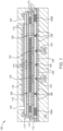
- FIG 1 is a schematic illustration of a MEMS device 100 prior to removing sacrificial material and releasing the beam.
- the MEMS device 100 includes a substrate 102, such as a CMOS substrate that includes numerous layers for a semiconductor device. It is also contemplated that the substrate 102 may simply be a semiconductor substrate containing silicon, germanium, or other suitable semiconductor material.
- the contact electrodes 104A, 104B may be RF conductors or RF electrodes. It is to be understood that while two contact electrodes 104A, 104B are shown, a single contact electrode, or even more than two contact electrodes is contemplated.
- the contact electrodes 104A, 104B may be comprised of any conductive material suitable for use in a semiconductor device such as copper, aluminum, titanium nitride, tungsten, and combinations thereof.
- Additional conductive material may be present on or above the substrate 102 as well as the contact electrodes 104A, 104B.
- anchor electrodes 106A, 106B are shown in Figure 1 , as are numerous additional electrical contacts 108.
- the anchor electrodes 106A, 106B are the electrodes for the beam structure 114, and the electrical contacts 108 may be used for pull-in electrodes.
- the anchor electrodes 106A, 106B and the electrical contacts 108 may be comprised of any conductive material suitable for use in a semiconductor device such as copper, aluminum, titanium nitride, tungsten, and combinations thereof.
- a dielectric layer 110 is present over the substrate 102, including over the electric contacts 108. It is contemplated that the dielectric layer 110 encompasses an electrically insulating material such as silicon oxide, silicon dioxide, silicon nitride, silicon oxynitride, or combinations thereof.
- a first sacrificial layer 112 is present over the dielectric layer 110.
- the first sacrificial layer 112 will ultimately be removed to free the beam structure 114.
- the first sacrificial layer 112 comprises a different material than the dielectric layer 110.
- Suitable material for the first sacrificial layer 112 includes spin-on material such as a carbon based material.
- the first sacrificial layer 112 may comprise carbon, hydrogen, nitrogen, and oxygen.
- a second dielectric layer 110 is present over the first sacrificial layer 112, and the bottom portion of the beam structure 114 is present over the second dielectric layer 110.
- the second dielectric layer 110 may comprise the same material as the first dielectric layer 110.
- the beam structure 114 may comprise any conductive material suitable for use in a semiconductor device such as copper, aluminum, titanium nitride (TiN), tungsten, titanium aluminum nitride (TiAlN), tantalum nitride (TaN), and combinations thereof.
- the beam structure 114 additionally includes a middle portion, a top portion, and post portions. Dielectric layers 110 are present on the top and bottom surfaces of the beam portions.
- additional sacrificial material 112 is present.
- the sacrificial material 112 may comprise the same material in all locations within the MEMS device 100. In fact, sacrificial material 112 is present over the top portion of the beam structure 114.
- an additional dielectric layer 110 is present on and in contact with the topmost sacrificial material 112, an additional dielectric layer 110 is present.
- a pull-up electrode 116 is present over and on the additional dielectric layer 110.
- a dielectric roof 118 is also present over the pull-up electrode 116.
- Release holes 120 are present through the dielectric roof 118 and the top-most dielectric layer 110. The release holes 120 extend through the roof 118 to expose the sacrificial material 112.
- the bottom of the beam structure 114 comprises two beam contact portions 122 that comprise ruthenium.
- Two electrical contact stacks containing contact surface 124 of ruthenium are present over each contact electrode 104A, 104B and aligned with the two beam contact portions 122.
- the contact surfaces 124 comprising ruthenium are the landing location for the beam structure 114, as will be discussed later.
- the beam contact portions 122 contact the contact surfaces 124 when the beam structure 114 has been freed and is in the pulled-down state, which is the maximum capacitance state.
- One or more additional electrical contact stacks containing contact surface 126 of ruthenium are disposed over a portion of the electrical contacts 108.
- FIG 2 is a schematic illustration of the MEMS device 100 of Figure 1 after the sacrificial material 112 has been removed and the beam 114 has been released.
- the sacrificial material 112 is removed by an etching process where the etchant, which may be a wet etchant or a dry etchant, is introduced through the release holes 120.
- the etchant which may be a wet etchant or a dry etchant
- the beam structure 114 is free to move within the cavity 202 once the sacrificial material 112 is removed.
- the beam structure 114 may move from a first position spaced from both the pull-up electrode 116 and the electrical contact stacks containing contact surface 124 of ruthenium (shown in Figure 2 ) back and forth as needed to a second position in contact with the contact surfaces 124 and a third position disposed adjacent to the pull-up electrode 116 and spaced a greater distance from the contact surfaces 124 than in the first position.
- the terms "first position”, “second position”, and “third position” are not intending to be limiting, and the beam structure 114 may move to and from any of the three positions in any order.
- the sacrificial material 112 is removed, but everything else in the device 100 remains.
- the contact surfaces 124, 126 are now exposed as are the contact portions 122 that contain ruthenium.
- ruthenium has low resistance and is a durable contact, but ruthenium contacts are susceptible to potential stiction events over operating life. Hence, it has been surprisingly found that additional treatment of the ruthenium will lead to less stiction and further lower the contact resistance of the device.
- the ruthenium comprising elements of the device 100 may be treated with a fluorine-based treatment.
- a plasma containing fluorine and oxygen may be optionally introduced to the cavity 202 through the release holes 120.
- the plasma is formed from O 2 and CF 4 .
- fluorine based gases such as NF 3 , SF 6 , and CHF 3 .
- a Fluorocarbon-based Self Assembled Monolayer SAM
- the disclosure is not to be limited to CF 4 .
- C x F y polymer formation formed during the introduction of the fluorine-based treatment may increase contact resistance to an unacceptable level.
- Excessive fluorine doping of ruthenium may increase contact resistance to an unacceptable level. Thus, as little polymer formation as possible is desired to maintain low contact resistance.
- Figure 3A is a zoomed-in schematic illustration of a portion of the MEMS device 100 of Figure 2 after the sacrificial material 112 has been removed and/or after the optional fluorine-based treatment.
- an interstitial layer 330 or layer of residue may be disposed on the top surface 332 of the contact surface 124.
- the interstitial layer 330 or layer of residue may form on the contact surfaces 124, 126 during the various formation operations of the MEMS device 100, such as during fabrication or construction, during removal of the sacrificial material 112, or during the optional fluorine-based treatment.
- a chlorine (Cl) etch process is performed.
- the chlorine etch process is performed prior to the optional fluorine-based treatment.
- the optional fluorine-based treatment may occur before or after the chlorine etch process.
- the chlorine etch process may occur following the removal of the sacrificial material 112.
- Etchant comprising chlorine, such as hydrochloric acid (HCl), boron trichloride (BCl 3 ), or chlorine gas (Cl 2 ), is introduced to cavity 202 through the release holes 120.
- the chlorine etch-back process may be a "wet" or a "dry” process.
- the dry etch-back process may include oxygen and/or a combination of oxygen and fluorine.
- the chlorine containing etchant has high etch selectivity such that the etchant etches only ruthenium comprising elements of the device 100 and residues such as the interstitial layer 330. Thus, the chlorine containing etchant etches a portion of the contact electrode surfaces 124, 126 and/or a bottom portion of the beam contact surfaces 122 without etching the beam structure 114 or the dielectric layers 110.
- the chlorine containing etch-back process has a very high selectivity (20:1) towards dielectrics, titanium, titanium nitride, and titanium aluminum nitride, which enables the etch-back process to selectively etch-back the contact electrode surfaces 124, 126 without negatively impacting other components inside the cavity.
- Figure 3B is a zoomed-in schematic illustration of the MEMS device 100 of Figure 2 after the exposed ruthenium comprising elements of the device 100 (i.e., the beam contact portions 122 and the contact surfaces 124, 126) have been etched.
- a top portion or surface 332 of the contact surfaces 124, 126 and a bottom portion or surface 334 of the beam contact portions 122 have been partially removed through the chlorine etch process.
- Figure 3B illustrates the removal of ruthenium from both the contact surfaces 124, 126 and the beam contact portions 122, the removal may occur only to the contact surfaces 124, 126, only to the beam contact portions 122, or to both the contact surfaces 124, 126 and the beam contact portions 122.
- Etching a bottom portion or surface 334 of the beam contact portions 122 recesses the beam contact portions 122 into the beam structure 114, and etching a top portion or surface 332 of the contact surfaces 124, 126 reduces the overall height of the contact electrodes.
- the exposed ruthenium comprising elements etched during the chlorine etch process i.e., the top surface 332 of the contact surfaces 124, 126 and/or the bottom surface 334 of the beam contact portions 122
- the top surface 332 of the contact surfaces 124, 126 and/or the bottom surface 334 of the beam contact portions 122 may have a surface with elevated roughness.
- the top surface 332 of the contact surfaces 124, 126 and/or the bottom surface 334 of the beam contact portions 122 have a surface roughness from being etched with the etchant containing chlorine.
- the top surface 332 and the bottom surface 334 each have a roughness root mean square of about 1 nm to about 10 nm, such as about 2 nm to about 5 nm.
- the surface roughness may increase with extended exposure of the surfaces 332, 334 to the etchant containing chlorine.
- any residues or interstitial layers 330 that may have formed during formation of the device 100 are removed from the exposed ruthenium comprising elements by pumping an inert gas, such as argon, into the cavity.
- the chlorine containing etchant has a ruthenium etch rate of about 2 nm/min to about 10 nm/min, such as about 4 nm/min, and a selectivity ratio for etching ruthenium to surrounding exposed materials, such as oxide, TiAlN, and TiN, of about 20:1 to about 25:1 (i.e., the chlorine containing etchant may etch ruthenium 20 to 25 times faster than the chlorine containing etchant etches oxide, TiAlN, and TiN).
- the etchant containing chlorine may be present in the cavity 202 for about 1 minute to 5 minutes, such as about 2.5 minutes to 3 minutes.
- the chlorine etch process may remove about 5 nm to 15 nm of ruthenium from each of the contact surfaces 124, 126 and the beam contact portions 122. By etching the ruthenium from the contact surfaces 124, 126 and the beam contact portions 122, the contact resistance of the MEMS device 100 is effectively lowered. In one embodiment, the chlorine etching process lowers the contact resistance of the device 100 by a factor of about 2 as compared to conventional MEMS devices.
- Etching a portion of the contact surfaces 124, 126 from each of the electrical contact stacks and/or a portion of each beam contact portion 122 cleans the ruthenium surfaces that were in contact with the sacrificial material 112.
- the chlorine etch process further removes any residues, interstitial layers, or interstitial impurities that may have formed on the surfaces while forming the MEMS device 100, such as during fabrication or construction, during removal of the sacrificial material 112, or during the optional fluorine containing plasma treatment.
- the chlorine etch process may remove any C x F y polymer formation that may have formed during the optional fluorine containing plasma treatment.
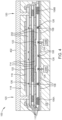
- FIG 4 is a schematic illustration of the MEMS device 100 of Figure 3B after the MEMS device has been sealed.
- a seal 402 is formed to seal the release holes 120.
- the seal 402 extends down to contact the top-most dielectric layer 110 disposed on the beam structure 114.
- the seal 402 may comprise a dielectric material such as silicon oxide, silicon dioxide, silicon nitride, silicon oxynitride, or combinations thereof.
- the resulting MEMS device will have contact surfaces that have low resistance, are durable, and are less susceptible to stiction events.
- a method of manufacturing a MEMS device comprises: forming one or more electrical contact stacks comprising a contact surface of ruthenium within a cavity; forming a beam structure over the one or more electrical contact stacks within the cavity, wherein the cavity contains sacrificial material; removing the sacrificial material from the cavity to free the beam to move within the cavity; etching a portion of the contact surface of ruthenium using an etchant comprising chlorine; and sealing the cavity.
- the etchant may further comprise oxygen or fluorine based gasses.
- the etchant may be present in the cavity for a period of between about 2.5 minutes and 3 minutes. About 5 nm to about 15 nm of the contact surface of ruthenium may be removed through the etching.
- the beam structure may include at least one contact portion comprising ruthenium.
- the etching the portion of the contact surface of ruthenium using the etchant comprising chlorine may further comprise etching a bottom portion of the at least one contact portion comprising ruthenium. Etching the portion of the at least one contact portion comprising ruthenium may recess the at least one contact portion comprising ruthenium into the beam structure.
- the MEMS device may include at least one contact electrode. At least one of the one or more electrical contact stacks comprising the contact surface of ruthenium may be formed over the at least one contact electrode.
- the method may further comprise introducing a plasma containing fluorine and oxygen into the cavity prior to etching the portion of the contact surface of ruthenium using the etchant comprising chlorine.
- the etchant comprising chlorine may comprise hydrochloric acid, boron trichloride, or chlorine gas.
- the etching the portion of the contact surface of ruthenium using the etchant comprising chlorine may further remove any residues or interstitial layers from the contact surface of ruthenium.
- the etchant comprising chlorine may have an etch rate of about 4 nanometers per minute to about 6 nanometers per minute.
- the etchant comprising chlorine may have a selectivity ratio for etching ruthenium to oxide or titanium aluminum nitride of about 20:1.
Landscapes
- Engineering & Computer Science (AREA)
- Microelectronics & Electronic Packaging (AREA)
- Manufacturing & Machinery (AREA)
- Computer Hardware Design (AREA)
- Physics & Mathematics (AREA)
- Electromagnetism (AREA)
- Micromachines (AREA)
Claims (13)
- Verfahren zur Herstellung einer MEMS-Vorrichtung (100), umfassend:Bilden eines oder mehrerer elektrischer Kontaktstapel, die eine Kontaktfläche (124) aus Ruthenium umfassen, wobei mindestens einer des einen oder der mehreren elektrischen Kontaktstapel über mindestens eine Kontaktelektrode (104A, 104B) gebildet wird;Bilden einer Balkenstruktur (114) über dem einen oder den mehreren elektrischen Kontaktstapeln;Entfernen von Opfermaterial (112), um die Balkenstruktur für die Bewegung innerhalb eines Hohlraums (202) freizugeben, wobei mindestens ein Kontaktabschnitt (122) der Balkenstruktur in der Lage ist, die Kontaktfläche der mindestens einen Kontaktelektrode zu kontaktieren;Ätzen eines Abschnitts der Kontaktfläche (124) aus Ruthenium innerhalb des Hohlraums (202) unter Verwendung eines Ätzmittels, das Chlor umfasst; undVersiegeln des Hohlraums.
- Verfahren nach Anspruch 1, wobei das Ätzmittel ferner Sauerstoff oder Gase auf Fluorbasis umfasst.
- Verfahren nach Anspruch 1, wobei das Ätzmittel innerhalb des Hohlraums (202) für einen Zeitraum zwischen 2,5 Minuten und 3 Minuten vorhanden ist.
- Verfahren nach Anspruch 1, wobei 5 nm bis 15 nm der Kontaktfläche (124) aus Ruthenium durch das Ätzen entfernt wird.
- Verfahren nach Anspruch 1, wobei die Balkenstruktur: (114) mindestens einen Kontaktabschnitt (122) beinhaltet, der Ruthenium umfasst.
- Verfahren nach Anspruch 5, wobei das Ätzen des Abschnitts der Kontaktfläche (124) aus Ruthenium unter Verwendung des Ätzmittels, das Chlor umfasst, ferner das Ätzen eines unteren Abschnitts des mindestens einen Kontaktabschnitts (122), der Ruthenium umfasst, umfasst.
- Verfahren nach Anspruch 6, wobei das Ätzen des Abschnitts des mindestens einen Kontaktabschnitts (122), der Ruthenium umfasst, den mindestens einen Kontaktabschnitt in die Balkenstruktur (114) versenkt.
- Verfahren nach Anspruch 1, ferner umfassend Einbringen eines Plasmas, das Fluor und Sauerstoff enthält, in den Hohlraum (202) vor dem Ätzen des Abschnitts der Kontaktfläche (124) aus Ruthenium unter Verwendung des Ätzmittels, das Chlor umfasst.
- Verfahren nach Anspruch 1, wobei das Ätzmittel, das Chlor umfasst, Salzsäure, Bortrichlorid oder Chlorgas umfasst.
- Verfahren nach Anspruch 1, wobei das Ätzen des Abschnitts der Kontaktfläche (124) aus Ruthenium unter Verwendung des Ätzmittels, das Chlor umfasst, ferner jegliche Rückstände oder interstitielle Schichten (330) von der Kontaktfläche aus Ruthenium entfernt.
- Verfahren nach Anspruch 1, wobei das Ätzmittel, das Chlor umfasst, eine Ätzrate von 4 Nanometern pro Minute bis 6 Nanometern pro Minute aufweist.
- Verfahren nach Anspruch 1, wobei das Ätzmittel, das Chlor umfasst, ein Selektivitätsverhältnis zum Ätzen von Ruthenium zu Sauerstoff oder Titanaluminiumnitrid von etwa 20:1 aufweist.
- MEMS-Vorrichtung, umfassend:mindestens eine Kontaktelektrode (104A, 104B); einen oder mehrere elektrische Kontaktstapel, die eine Kontaktfläche (124) aus Ruthenium umfassen, wobei mindestens einer des einen oder der mehreren elektrischen Kontaktstapel über die mindestens eine Kontaktelektrode gebildet wird;eine Balkenstruktur (114) über dem einen oder den mehreren elektrischen Kontaktstapeln; undeinen versiegelten Hohlraum (202);wobei die MEMS-Vorrichtung durch das Verfahren nach Anspruch 1 hergestellt wird.
Priority Applications (1)
| Application Number | Priority Date | Filing Date | Title |
|---|---|---|---|
| EP24214547.2A EP4495965A3 (de) | 2019-05-30 | 2020-05-29 | Mems-vorrichtung mit verringertem kontaktwiderstand |
Applications Claiming Priority (2)
| Application Number | Priority Date | Filing Date | Title |
|---|---|---|---|
| US201962854826P | 2019-05-30 | 2019-05-30 | |
| PCT/US2020/035263 WO2020243529A1 (en) | 2019-05-30 | 2020-05-29 | Mems device having decreased contact resistance |
Related Child Applications (1)
| Application Number | Title | Priority Date | Filing Date |
|---|---|---|---|
| EP24214547.2A Division EP4495965A3 (de) | 2019-05-30 | 2020-05-29 | Mems-vorrichtung mit verringertem kontaktwiderstand |
Publications (2)
| Publication Number | Publication Date |
|---|---|
| EP3976527A1 EP3976527A1 (de) | 2022-04-06 |
| EP3976527B1 true EP3976527B1 (de) | 2024-12-18 |
Family
ID=71787087
Family Applications (2)
| Application Number | Title | Priority Date | Filing Date |
|---|---|---|---|
| EP24214547.2A Pending EP4495965A3 (de) | 2019-05-30 | 2020-05-29 | Mems-vorrichtung mit verringertem kontaktwiderstand |
| EP20746388.6A Active EP3976527B1 (de) | 2019-05-30 | 2020-05-29 | Mems-vorrichtung mit verringertem kontaktwiderstand |
Family Applications Before (1)
| Application Number | Title | Priority Date | Filing Date |
|---|---|---|---|
| EP24214547.2A Pending EP4495965A3 (de) | 2019-05-30 | 2020-05-29 | Mems-vorrichtung mit verringertem kontaktwiderstand |
Country Status (5)
| Country | Link |
|---|---|
| US (1) | US12077431B2 (de) |
| EP (2) | EP4495965A3 (de) |
| JP (1) | JP7588093B2 (de) |
| CN (1) | CN113748081B (de) |
| WO (1) | WO2020243529A1 (de) |
Family Cites Families (10)
| Publication number | Priority date | Publication date | Assignee | Title |
|---|---|---|---|---|
| US7256669B2 (en) | 2000-04-28 | 2007-08-14 | Northeastern University | Method of preparing electrical contacts used in switches |
| JP2009510707A (ja) | 2005-10-03 | 2009-03-12 | アナログ デバイシス, インコーポレイテッド | Memsスイッチ接点システム |
| US8432239B2 (en) * | 2006-11-20 | 2013-04-30 | Massachusetts Institute Of Technology | Micro-electro mechanical tunneling switch |
| WO2008124372A2 (en) * | 2007-04-04 | 2008-10-16 | Qualcomm Mems Technologies, Inc. | Eliminate release etch attack by interface modification in sacrificial layers |
| US9892879B2 (en) | 2011-01-11 | 2018-02-13 | Qorvo Us, Inc. | Encapsulated micro-electromechanical system switch and method of manufacturing the same |
| US9040854B2 (en) * | 2011-09-13 | 2015-05-26 | Texas Instruments Incorporated | MEMS electrostatic actuator |
| JP6028969B2 (ja) | 2012-08-24 | 2016-11-24 | 国立大学法人大阪大学 | 結晶基板に孔を形成する方法、並びに結晶基板内に配線や配管を有する機能性デバイス |
| US20140264655A1 (en) * | 2013-03-13 | 2014-09-18 | Invensense, Inc. | Surface roughening to reduce adhesion in an integrated mems device |
| JP2016062984A (ja) | 2014-09-16 | 2016-04-25 | 株式会社リコー | 圧電アクチュエータ及びその製造方法及び液体カートリッジ及び画像形成装置 |
| US10273141B2 (en) * | 2016-04-26 | 2019-04-30 | Taiwan Semiconductor Manufacturing Co., Ltd. | Rough layer for better anti-stiction deposition |
-
2020
- 2020-05-29 JP JP2021566474A patent/JP7588093B2/ja active Active
- 2020-05-29 EP EP24214547.2A patent/EP4495965A3/de active Pending
- 2020-05-29 EP EP20746388.6A patent/EP3976527B1/de active Active
- 2020-05-29 WO PCT/US2020/035263 patent/WO2020243529A1/en not_active Ceased
- 2020-05-29 US US17/608,822 patent/US12077431B2/en active Active
- 2020-05-29 CN CN202080032167.XA patent/CN113748081B/zh active Active
Also Published As
| Publication number | Publication date |
|---|---|
| EP3976527A1 (de) | 2022-04-06 |
| EP4495965A2 (de) | 2025-01-22 |
| JP2022534675A (ja) | 2022-08-03 |
| WO2020243529A1 (en) | 2020-12-03 |
| CN113748081A (zh) | 2021-12-03 |
| US12077431B2 (en) | 2024-09-03 |
| US20220289565A1 (en) | 2022-09-15 |
| EP4495965A3 (de) | 2025-04-23 |
| JP7588093B2 (ja) | 2024-11-21 |
| CN113748081B (zh) | 2025-07-15 |
Similar Documents
| Publication | Publication Date | Title |
|---|---|---|
| CN112750760B (zh) | 自对准双图案化 | |
| US8153527B2 (en) | Method for reducing sidewall etch residue | |
| KR20080013174A (ko) | 캐패시터의 스토리지노드 분리 방법 | |
| US20090124082A1 (en) | Slurry for polishing ruthenium and method for polishing using the same | |
| JP2010199136A (ja) | キャパシタの製造方法 | |
| US6191047B1 (en) | Etching process using a buffer layer | |
| EP3976527B1 (de) | Mems-vorrichtung mit verringertem kontaktwiderstand | |
| CN1581493A (zh) | 半导体电容器结构及其制造方法 | |
| US7741223B2 (en) | Semiconductor device with bulb type recess gate and method for fabricating the same | |
| US12172888B2 (en) | Anti-stiction enhancement of ruthenium contact | |
| JP4542488B2 (ja) | 半導体装置の製造方法 | |
| JP2002208633A (ja) | 半導体装置およびその製造方法 | |
| KR20100034629A (ko) | 캐패시터 제조 방법 | |
| KR100492899B1 (ko) | 반도체소자 및 그 제조 방법 | |
| KR100875658B1 (ko) | 반도체소자 제조방법 | |
| KR100511908B1 (ko) | 다마신 및 자기 정렬 콘택 공정을 이용한 반도체 소자의제조방법 | |
| KR100518527B1 (ko) | 저저항의 게이트 전극을 갖는 반도체 소자의 제조방법 | |
| KR20060004508A (ko) | 커패시터 제조 방법 | |
| KR101073129B1 (ko) | 캐패시터의 스토리지노드 분리 방법 | |
| KR100683486B1 (ko) | 반도체 소자의 캐패시터 제조방법 | |
| KR100812599B1 (ko) | 반도체 소자의 전하저장전극 형성방법 | |
| KR20030002753A (ko) | 캐패시터의 스토러지 노드 전극 형성 방법 | |
| KR20000004593A (ko) | 반도체 소자의 전하저장전극 형성방법 | |
| KR20120102441A (ko) | 반도체 소자의 커패시터 형성 방법 | |
| KR20070064837A (ko) | 반도체 소자의 캐패시터 제조 방법 |
Legal Events
| Date | Code | Title | Description |
|---|---|---|---|
| STAA | Information on the status of an ep patent application or granted ep patent |
Free format text: STATUS: UNKNOWN |
|
| STAA | Information on the status of an ep patent application or granted ep patent |
Free format text: STATUS: THE INTERNATIONAL PUBLICATION HAS BEEN MADE |
|
| PUAI | Public reference made under article 153(3) epc to a published international application that has entered the european phase |
Free format text: ORIGINAL CODE: 0009012 |
|
| STAA | Information on the status of an ep patent application or granted ep patent |
Free format text: STATUS: REQUEST FOR EXAMINATION WAS MADE |
|
| 17P | Request for examination filed |
Effective date: 20211022 |
|
| AK | Designated contracting states |
Kind code of ref document: A1 Designated state(s): AL AT BE BG CH CY CZ DE DK EE ES FI FR GB GR HR HU IE IS IT LI LT LU LV MC MK MT NL NO PL PT RO RS SE SI SK SM TR |
|
| DAV | Request for validation of the european patent (deleted) | ||
| DAX | Request for extension of the european patent (deleted) | ||
| P01 | Opt-out of the competence of the unified patent court (upc) registered |
Effective date: 20230515 |
|
| GRAP | Despatch of communication of intention to grant a patent |
Free format text: ORIGINAL CODE: EPIDOSNIGR1 |
|
| STAA | Information on the status of an ep patent application or granted ep patent |
Free format text: STATUS: GRANT OF PATENT IS INTENDED |
|
| INTG | Intention to grant announced |
Effective date: 20240711 |
|
| GRAS | Grant fee paid |
Free format text: ORIGINAL CODE: EPIDOSNIGR3 |
|
| GRAA | (expected) grant |
Free format text: ORIGINAL CODE: 0009210 |
|
| STAA | Information on the status of an ep patent application or granted ep patent |
Free format text: STATUS: THE PATENT HAS BEEN GRANTED |
|
| AK | Designated contracting states |
Kind code of ref document: B1 Designated state(s): AL AT BE BG CH CY CZ DE DK EE ES FI FR GB GR HR HU IE IS IT LI LT LU LV MC MK MT NL NO PL PT RO RS SE SI SK SM TR |
|
| REG | Reference to a national code |
Ref country code: CH Ref legal event code: EP |
|
| REG | Reference to a national code |
Ref country code: DE Ref legal event code: R096 Ref document number: 602020043361 Country of ref document: DE |
|
| REG | Reference to a national code |
Ref country code: IE Ref legal event code: FG4D |
|
| REG | Reference to a national code |
Ref country code: LT Ref legal event code: MG9D |
|
| PG25 | Lapsed in a contracting state [announced via postgrant information from national office to epo] |
Ref country code: HR Free format text: LAPSE BECAUSE OF FAILURE TO SUBMIT A TRANSLATION OF THE DESCRIPTION OR TO PAY THE FEE WITHIN THE PRESCRIBED TIME-LIMIT Effective date: 20241218 |
|
| PG25 | Lapsed in a contracting state [announced via postgrant information from national office to epo] |
Ref country code: FI Free format text: LAPSE BECAUSE OF FAILURE TO SUBMIT A TRANSLATION OF THE DESCRIPTION OR TO PAY THE FEE WITHIN THE PRESCRIBED TIME-LIMIT Effective date: 20241218 |
|
| PG25 | Lapsed in a contracting state [announced via postgrant information from national office to epo] |
Ref country code: BG Free format text: LAPSE BECAUSE OF FAILURE TO SUBMIT A TRANSLATION OF THE DESCRIPTION OR TO PAY THE FEE WITHIN THE PRESCRIBED TIME-LIMIT Effective date: 20241218 |
|
| PG25 | Lapsed in a contracting state [announced via postgrant information from national office to epo] |
Ref country code: NO Free format text: LAPSE BECAUSE OF FAILURE TO SUBMIT A TRANSLATION OF THE DESCRIPTION OR TO PAY THE FEE WITHIN THE PRESCRIBED TIME-LIMIT Effective date: 20250318 |
|
| REG | Reference to a national code |
Ref country code: NL Ref legal event code: MP Effective date: 20241218 |
|
| PG25 | Lapsed in a contracting state [announced via postgrant information from national office to epo] |
Ref country code: LV Free format text: LAPSE BECAUSE OF FAILURE TO SUBMIT A TRANSLATION OF THE DESCRIPTION OR TO PAY THE FEE WITHIN THE PRESCRIBED TIME-LIMIT Effective date: 20241218 Ref country code: GR Free format text: LAPSE BECAUSE OF FAILURE TO SUBMIT A TRANSLATION OF THE DESCRIPTION OR TO PAY THE FEE WITHIN THE PRESCRIBED TIME-LIMIT Effective date: 20250319 |
|
| PG25 | Lapsed in a contracting state [announced via postgrant information from national office to epo] |
Ref country code: RS Free format text: LAPSE BECAUSE OF FAILURE TO SUBMIT A TRANSLATION OF THE DESCRIPTION OR TO PAY THE FEE WITHIN THE PRESCRIBED TIME-LIMIT Effective date: 20250318 |
|
| PG25 | Lapsed in a contracting state [announced via postgrant information from national office to epo] |
Ref country code: NL Free format text: LAPSE BECAUSE OF FAILURE TO SUBMIT A TRANSLATION OF THE DESCRIPTION OR TO PAY THE FEE WITHIN THE PRESCRIBED TIME-LIMIT Effective date: 20241218 |
|
| REG | Reference to a national code |
Ref country code: AT Ref legal event code: MK05 Ref document number: 1752139 Country of ref document: AT Kind code of ref document: T Effective date: 20241218 |
|
| PG25 | Lapsed in a contracting state [announced via postgrant information from national office to epo] |
Ref country code: SM Free format text: LAPSE BECAUSE OF FAILURE TO SUBMIT A TRANSLATION OF THE DESCRIPTION OR TO PAY THE FEE WITHIN THE PRESCRIBED TIME-LIMIT Effective date: 20241218 |
|
| PG25 | Lapsed in a contracting state [announced via postgrant information from national office to epo] |
Ref country code: PL Free format text: LAPSE BECAUSE OF FAILURE TO SUBMIT A TRANSLATION OF THE DESCRIPTION OR TO PAY THE FEE WITHIN THE PRESCRIBED TIME-LIMIT Effective date: 20241218 |
|
| PGFP | Annual fee paid to national office [announced via postgrant information from national office to epo] |
Ref country code: DE Payment date: 20250530 Year of fee payment: 6 |
|
| PG25 | Lapsed in a contracting state [announced via postgrant information from national office to epo] |
Ref country code: ES Free format text: LAPSE BECAUSE OF FAILURE TO SUBMIT A TRANSLATION OF THE DESCRIPTION OR TO PAY THE FEE WITHIN THE PRESCRIBED TIME-LIMIT Effective date: 20241218 |
|
| PG25 | Lapsed in a contracting state [announced via postgrant information from national office to epo] |
Ref country code: IS Free format text: LAPSE BECAUSE OF FAILURE TO SUBMIT A TRANSLATION OF THE DESCRIPTION OR TO PAY THE FEE WITHIN THE PRESCRIBED TIME-LIMIT Effective date: 20250418 |
|
| PG25 | Lapsed in a contracting state [announced via postgrant information from national office to epo] |
Ref country code: PT Free format text: LAPSE BECAUSE OF FAILURE TO SUBMIT A TRANSLATION OF THE DESCRIPTION OR TO PAY THE FEE WITHIN THE PRESCRIBED TIME-LIMIT Effective date: 20250421 |
|
| PG25 | Lapsed in a contracting state [announced via postgrant information from national office to epo] |
Ref country code: EE Free format text: LAPSE BECAUSE OF FAILURE TO SUBMIT A TRANSLATION OF THE DESCRIPTION OR TO PAY THE FEE WITHIN THE PRESCRIBED TIME-LIMIT Effective date: 20241218 |
|
| PG25 | Lapsed in a contracting state [announced via postgrant information from national office to epo] |
Ref country code: RO Free format text: LAPSE BECAUSE OF FAILURE TO SUBMIT A TRANSLATION OF THE DESCRIPTION OR TO PAY THE FEE WITHIN THE PRESCRIBED TIME-LIMIT Effective date: 20241218 Ref country code: AT Free format text: LAPSE BECAUSE OF FAILURE TO SUBMIT A TRANSLATION OF THE DESCRIPTION OR TO PAY THE FEE WITHIN THE PRESCRIBED TIME-LIMIT Effective date: 20241218 |
|
| PG25 | Lapsed in a contracting state [announced via postgrant information from national office to epo] |
Ref country code: SK Free format text: LAPSE BECAUSE OF FAILURE TO SUBMIT A TRANSLATION OF THE DESCRIPTION OR TO PAY THE FEE WITHIN THE PRESCRIBED TIME-LIMIT Effective date: 20241218 |
|
| PG25 | Lapsed in a contracting state [announced via postgrant information from national office to epo] |
Ref country code: CZ Free format text: LAPSE BECAUSE OF FAILURE TO SUBMIT A TRANSLATION OF THE DESCRIPTION OR TO PAY THE FEE WITHIN THE PRESCRIBED TIME-LIMIT Effective date: 20241218 |
|
| PG25 | Lapsed in a contracting state [announced via postgrant information from national office to epo] |
Ref country code: IT Free format text: LAPSE BECAUSE OF FAILURE TO SUBMIT A TRANSLATION OF THE DESCRIPTION OR TO PAY THE FEE WITHIN THE PRESCRIBED TIME-LIMIT Effective date: 20241218 |
|
| PG25 | Lapsed in a contracting state [announced via postgrant information from national office to epo] |
Ref country code: SE Free format text: LAPSE BECAUSE OF FAILURE TO SUBMIT A TRANSLATION OF THE DESCRIPTION OR TO PAY THE FEE WITHIN THE PRESCRIBED TIME-LIMIT Effective date: 20241218 |
|
| REG | Reference to a national code |
Ref country code: DE Ref legal event code: R097 Ref document number: 602020043361 Country of ref document: DE |
|
| PG25 | Lapsed in a contracting state [announced via postgrant information from national office to epo] |
Ref country code: DK Free format text: LAPSE BECAUSE OF FAILURE TO SUBMIT A TRANSLATION OF THE DESCRIPTION OR TO PAY THE FEE WITHIN THE PRESCRIBED TIME-LIMIT Effective date: 20241218 |
|
| PLBE | No opposition filed within time limit |
Free format text: ORIGINAL CODE: 0009261 |
|
| STAA | Information on the status of an ep patent application or granted ep patent |
Free format text: STATUS: NO OPPOSITION FILED WITHIN TIME LIMIT |
|
| REG | Reference to a national code |
Ref country code: CH Ref legal event code: L10 Free format text: ST27 STATUS EVENT CODE: U-0-0-L10-L00 (AS PROVIDED BY THE NATIONAL OFFICE) Effective date: 20251029 |
|
| 26N | No opposition filed |
Effective date: 20250919 |
|
| REG | Reference to a national code |
Ref country code: CH Ref legal event code: H13 Free format text: ST27 STATUS EVENT CODE: U-0-0-H10-H13 (AS PROVIDED BY THE NATIONAL OFFICE) Effective date: 20251223 |
|
| PG25 | Lapsed in a contracting state [announced via postgrant information from national office to epo] |
Ref country code: LU Free format text: LAPSE BECAUSE OF NON-PAYMENT OF DUE FEES Effective date: 20250529 |
|
| PG25 | Lapsed in a contracting state [announced via postgrant information from national office to epo] |
Ref country code: CH Free format text: LAPSE BECAUSE OF NON-PAYMENT OF DUE FEES Effective date: 20250531 |
|
| GBPC | Gb: european patent ceased through non-payment of renewal fee |
Effective date: 20250529 |
|
| REG | Reference to a national code |
Ref country code: BE Ref legal event code: MM Effective date: 20250531 |
|
| PG25 | Lapsed in a contracting state [announced via postgrant information from national office to epo] |
Ref country code: MC Free format text: LAPSE BECAUSE OF FAILURE TO SUBMIT A TRANSLATION OF THE DESCRIPTION OR TO PAY THE FEE WITHIN THE PRESCRIBED TIME-LIMIT Effective date: 20241218 |
|
| PG25 | Lapsed in a contracting state [announced via postgrant information from national office to epo] |
Ref country code: GB Free format text: LAPSE BECAUSE OF NON-PAYMENT OF DUE FEES Effective date: 20250529 |
|
| PG25 | Lapsed in a contracting state [announced via postgrant information from national office to epo] |
Ref country code: IE Free format text: LAPSE BECAUSE OF NON-PAYMENT OF DUE FEES Effective date: 20250529 |
|
| PG25 | Lapsed in a contracting state [announced via postgrant information from national office to epo] |
Ref country code: BE Free format text: LAPSE BECAUSE OF NON-PAYMENT OF DUE FEES Effective date: 20250531 |
|
| PG25 | Lapsed in a contracting state [announced via postgrant information from national office to epo] |
Ref country code: FR Free format text: LAPSE BECAUSE OF NON-PAYMENT OF DUE FEES Effective date: 20250531 |