EP3971990A1 - Halbleiterstruktur und verfahren zur herstellung davon - Google Patents
Halbleiterstruktur und verfahren zur herstellung davon Download PDFInfo
- Publication number
- EP3971990A1 EP3971990A1 EP21784007.3A EP21784007A EP3971990A1 EP 3971990 A1 EP3971990 A1 EP 3971990A1 EP 21784007 A EP21784007 A EP 21784007A EP 3971990 A1 EP3971990 A1 EP 3971990A1
- Authority
- EP
- European Patent Office
- Prior art keywords
- conductive layer
- layer
- trench
- dielectric layer
- equipotential
- Prior art date
- Legal status (The legal status is an assumption and is not a legal conclusion. Google has not performed a legal analysis and makes no representation as to the accuracy of the status listed.)
- Granted
Links
Images


Classifications
-
- H—ELECTRICITY
- H10—SEMICONDUCTOR DEVICES; ELECTRIC SOLID-STATE DEVICES NOT OTHERWISE PROVIDED FOR
- H10B—ELECTRONIC MEMORY DEVICES
- H10B12/00—Dynamic random access memory [DRAM] devices
- H10B12/30—DRAM devices comprising one-transistor - one-capacitor [1T-1C] memory cells
- H10B12/34—DRAM devices comprising one-transistor - one-capacitor [1T-1C] memory cells the transistor being at least partially in a trench in the substrate
-
- H—ELECTRICITY
- H10—SEMICONDUCTOR DEVICES; ELECTRIC SOLID-STATE DEVICES NOT OTHERWISE PROVIDED FOR
- H10D—INORGANIC ELECTRIC SEMICONDUCTOR DEVICES
- H10D64/00—Electrodes of devices having potential barriers
- H10D64/60—Electrodes characterised by their materials
- H10D64/66—Electrodes having a conductor capacitively coupled to a semiconductor by an insulator, e.g. MIS electrodes
- H10D64/68—Electrodes having a conductor capacitively coupled to a semiconductor by an insulator, e.g. MIS electrodes characterised by the insulator, e.g. by the gate insulator
- H10D64/681—Electrodes having a conductor capacitively coupled to a semiconductor by an insulator, e.g. MIS electrodes characterised by the insulator, e.g. by the gate insulator having a compositional variation, e.g. multilayered
-
- H—ELECTRICITY
- H10—SEMICONDUCTOR DEVICES; ELECTRIC SOLID-STATE DEVICES NOT OTHERWISE PROVIDED FOR
- H10B—ELECTRONIC MEMORY DEVICES
- H10B12/00—Dynamic random access memory [DRAM] devices
- H10B12/01—Manufacture or treatment
- H10B12/02—Manufacture or treatment for one transistor one-capacitor [1T-1C] memory cells
- H10B12/05—Making the transistor
- H10B12/053—Making the transistor the transistor being at least partially in a trench in the substrate
-
- H—ELECTRICITY
- H10—SEMICONDUCTOR DEVICES; ELECTRIC SOLID-STATE DEVICES NOT OTHERWISE PROVIDED FOR
- H10B—ELECTRONIC MEMORY DEVICES
- H10B12/00—Dynamic random access memory [DRAM] devices
- H10B12/30—DRAM devices comprising one-transistor - one-capacitor [1T-1C] memory cells
- H10B12/48—Data lines or contacts therefor
- H10B12/485—Bit line contacts
-
- H—ELECTRICITY
- H10—SEMICONDUCTOR DEVICES; ELECTRIC SOLID-STATE DEVICES NOT OTHERWISE PROVIDED FOR
- H10B—ELECTRONIC MEMORY DEVICES
- H10B12/00—Dynamic random access memory [DRAM] devices
- H10B12/30—DRAM devices comprising one-transistor - one-capacitor [1T-1C] memory cells
- H10B12/48—Data lines or contacts therefor
- H10B12/488—Word lines
-
- H—ELECTRICITY
- H10—SEMICONDUCTOR DEVICES; ELECTRIC SOLID-STATE DEVICES NOT OTHERWISE PROVIDED FOR
- H10D—INORGANIC ELECTRIC SEMICONDUCTOR DEVICES
- H10D64/00—Electrodes of devices having potential barriers
- H10D64/01—Manufacture or treatment
- H10D64/013—Manufacture or treatment of electrodes having a conductor capacitively coupled to a semiconductor by an insulator
- H10D64/01302—Manufacture or treatment of electrodes having a conductor capacitively coupled to a semiconductor by an insulator the insulator being formed after the semiconductor body, the semiconductor being silicon
- H10D64/01332—Making the insulator
-
- H—ELECTRICITY
- H10—SEMICONDUCTOR DEVICES; ELECTRIC SOLID-STATE DEVICES NOT OTHERWISE PROVIDED FOR
- H10D—INORGANIC ELECTRIC SEMICONDUCTOR DEVICES
- H10D64/00—Electrodes of devices having potential barriers
- H10D64/20—Electrodes characterised by their shapes, relative sizes or dispositions
- H10D64/27—Electrodes not carrying the current to be rectified, amplified, oscillated or switched, e.g. gates
- H10D64/311—Gate electrodes for field-effect devices
- H10D64/411—Gate electrodes for field-effect devices for FETs
- H10D64/511—Gate electrodes for field-effect devices for FETs for IGFETs
- H10D64/512—Disposition of the gate electrodes, e.g. buried gates
- H10D64/513—Disposition of the gate electrodes, e.g. buried gates within recesses in the substrate, e.g. trench gates, groove gates or buried gates
Definitions
- the present invention relates to the field of semiconductor technology, in particular to a semiconductor structure and a method of manufacturing the same.
- a dual work-function gate evolves as the mainstream of the buried word line, wherein the dual work-function gate includes a first conductive layer and a second conductive layer stacked on the first conductive layer.
- the conductive materials in the first conductive layer have a problem of diffusing into the second conductive layer.
- the metal in the metal layer diffuses more significantly into the polycrystalline silicon layer after experiencing a thermal process, resulting in a problem of affecting the performance of the polycrystalline silicon layer.
- a semiconductor structure and a method of manufacturing the same are provided to prevent the conductive materials in a first conductive layer from diffusing into a second conductive layer, and improve the performance of the device.
- a method of manufacturing a semiconductor structure comprising:
- the dielectric layer is an equipotential dielectric layer, the equipotential dielectric layer is configured to cause potential of the first conductive layer equal to potential of the second conductive layer.
- the equipotential dielectric layer has a thickness less than 20nm.
- the method further comprises forming a first dielectric layer on surface of the trench, wherein the first dielectric layer extends to the top of the trench.
- the method further comprises forming a source on one side of the trench and a drain on the other side of the trench respectively, wherein bottom of the source being lower than bottom of the drain, and the bottom of the drain being at same height as the equipotential dielectric layer.
- the method further comprises forming a bit line connecting plug on the source and forming a storage node plug on the drain.
- the method further comprises forming a barrier layer on a surface of the first dielectric layer, wherein the barrier layer is located between the first conductive layer and the first dielectric layer, and extends to the top of the first conductive layer.
- forming a dielectric layer on the first conductive layer comprises: forming an equipotential dielectric material layer by a deposition process, wherein the equipotential dielectric material layer covering upper surface of the first conductive layer, upper surface of the substrate, and side walls of the trench; and removing the equipotential dielectric material layer located on the upper surface of the substrate, so as to form the equipotential dielectric layer covering the upper surface of the first conductive layer and the side walls of the trench above the first conductive layer.
- the deposition process is selected from one of an atomic layer deposition (ALD), a plasma enhanced chemical vapor deposition (PECVD), a low pressure chemical vapor deposition (LPCVD), and a metal-organic chemical vapor deposition (MOCVD).
- ALD atomic layer deposition
- PECVD plasma enhanced chemical vapor deposition
- LPCVD low pressure chemical vapor deposition
- MOCVD metal-organic chemical vapor deposition
- a semiconductor structure comprising:
- the dielectric layer is an equipotential dielectric layer causing potential of the first conductive layer equal to potential of the second conductive layer.
- the equipotential dielectric layer has a thickness less than 20nm.
- the equipotential dielectric layer has a thickness range of 1-8nm.
- material of the equipotential dielectric layer is insulating material.
- the insulating material is selected from one of silicon oxide, silicon nitride, silicon oxynitride, silicon carbonoxide, and silicon carbonitride, or their combination.
- the first conductive layer is a metal conductive layer
- the second conductive layer is a semiconductor conductive layer
- material of the metal conductive layer is selected from one of tungsten, cobalt, manganese, niobium, nickel, and molybdenum, or their combination; and material of the semiconductor conductive layer is selected from one of polycrystalline silicon, silicon germanide, gallium arsenide, gallium phosphide, cadmium sulphide, and zinc sulphide, or their combination.
- the semiconductor structure further comprises a source located on one side of the trench and a drain located on the other side of the trench respectively, wherein bottom of the source being lower than bottom of the drain, and the bottom of the drain being at same height as the equipotential dielectric layer.
- the semiconductor structure further comprises a bit line connecting plug located on the source and a storage node plug located on the drain.
- the semiconductor structure further comprises a first dielectric layer located on the surface of the trench and extending to the top of the trench.
- the semiconductor structure further comprises a barrier layer located between the first conductive layer and the first dielectric layer and extending to the top of the first conductive layer.
- the dielectric layer is also located on side walls of the trench above the first conductive layer.
- a semiconductor structure and a method of manufacturing the same By disposing between the first conductive layer and the second conductive layer the dielectric layer as a barrier layer so as to prevent the conductive materials in the first conductive layer from diffusing into the second conductive layer, and connecting the first conductive layer to the second conductive layer so as to form an equipotential, the performance of the device is improved.
- a method of manufacturing a semiconductor structure according to an embodiment includes the following steps:
- the performances of the first conductive layer 200 and the second conductive layer 400 are ensured by disposing between the first conductive layer 200 and the second conductive layer 400 the dielectric layer 300 as a barrier layer so as to prevent the conductive materials in the first conductive layer 200 from diffusing into the second conductive layer 400.
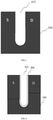
- the step S110 of providing a substrate 100 with a trench 103 is performed and may include the following steps.
- Step 1 a substrate 100 is provided.
- the substrate 100 may be, but not limited to, a silicon substrate, an epitaxial silicon substrate, a silicon-germanium substrate, a silicon-coated insulating substrate, or any substrate for bearing the components of the semiconductor integrated circuit, as well known by the person skilled in the art.
- a shallow trench isolation (STI) structure and active areas AAs are formed on the substrate 100, wherein the shallow trench isolation structure isolates the active areas from the ambient environment.
- the active area may be either a fin-like three-dimensional structure or a planar structure.
- the shallow trench isolation structure may isolate the active areas into an array arrangement, thereby manufacturing the storage array of the memory.
- the shallow trench isolation structure may include shallow trenches located in the substrate 100 and isolation materials filling the shallow trenches.
- the isolation materials may include line oxide formed and covering the shallow trench by the thermal oxidation process and silicon oxide located on the surface of the line oxide layer and filling up the shallow trench, thereby improving the isolation performance of the shallow trench isolation structure.
- Step 2 referring to Fig. 3 , a trench 103 is formed on the substrate 100.
- the trench 103 is formed on the active area AA of the substrate 100.
- the forming process includes the following steps. (1) A hard mask layer is formed.
- the hard mask layer may be formed by utilizing the deposition process to deposit insulating material on the surface having the shallow trench isolation structure and a pad oxide layer.
- the deposition process includes chemical vapor deposition (CVD), physical vapor deposition (PVD), atomic layer deposition (ALD), or the like.
- the insulating materials usually adopted include at least one of silicon nitride, silicon oxynitride, silicon carbonoxide, metal nitride, metal oxide and metal carbide, preferably silicon nitride (SiN), because the SiN material is easily available and has advantages of low cost, mature manufacturing approaches, etc., and also has a high etch selectivity ratio with silicon oxide in the pad oxide layer.
- SiN silicon nitride
- the hard mask layer is patterned to form an opening pattern passing through the hard mask layer.
- a matched mask can be utilized to form a pattern for defining the trench by a series of photolithographic processes, such as coating photoresist, exposure, and develop.
- the hard mask layer is etched to the surface of the pad oxide layer, so as to form a patterned hard mask layer having the opening pattern.
- the photoresist is removed, and the patterned hard mask layer serves as a mask to etch down further, so as to form the trench 103 in the active area AA of the substrate 100.
- a plurality of active areas AAs are distributed in an array, and a single active area AA is strip-like.
- the number of trenches formed on a single active area AA is unlimited. For example, two trenches are formed in a single active area AA.
- the active areas AAs are an array of active areas for DRAM storage, and the word line trenches for burying the gates are formed on the active areas AAs.
- the word line trenches are equally spaced and in parallel arrangement, and a single active area AA is provided with two word line trenches.
- the active area AA is doped to form a source S on one side of the trench 103 and/or a drain D on the other side of the trench 103 respectively.
- a common source S is formed between the two trenches, and drains D correspond to the outer sides of the two trenches.
- the time of forming the source S and the drain D during the process flow may be adjusted according to the practical situation of the process, which is not limited herein.
- the source S and the drain D may also be formed after the trench 103 is formed, or may further be formed after the second conductive layer is formed.
- Step 3 the pad oxide layer, the hard mask layer, etc. on the surface of the substrate 100 are removed by the etch process, the chemical-mechanical planarization process, or the like, and cleaning is further conducted to expose the clean surfaces of the active areas and the side walls and bottom surface of the trench 103.
- the step S120 of forming a first conductive layer 200 in the trench 103 is performed, wherein the top of the first conductive layer 200 is lower than the top of the trench 103.
- the method further includes:
- a first dielectric layer 500 is formed on the side walls and bottom of the trench 103, wherein the first dielectric layer 500 covers the side walls and bottom of the trench 103 and extends to the top of the trench 103.
- the first dielectric layer is a gate dielectric layer; the first dielectric layer 500 may be formed by utilizing the deposition process or the thermal oxidation process to form a silicon oxide material layer on the substrate 100 and the side walls and bottom of the trench 103, and then utilizing the etch process or the chemical-mechanical grinding process to remove the silicon oxide material on the surface of the substrate 100, while retaining the silicon oxide material layer on the side walls and bottom of the trench 103.
- dielectric materials of high K (the dielectric constant is greater than 7) may also be used to replace the silicon oxide material.
- dielectric materials of high K include Ta 2 O 5 , TiO 2 , TiN, Al 2 O 3 , Pr 2 O 3 , La 2 O 3 , LaAlO 3 , HfO 2 , ZrO 2 , or metal oxide of other constituents.
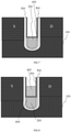
- the step of forming a first conductive layer 200 in the trench 103 further includes: forming a barrier material layer 600a, wherein the barrier material layer 600a covers the substrate 100 and the surface of the first dielectric layer 500 on the side walls and bottom of the trench 103; forming a first conductive material layer 200a for filling the trench 103, wherein the first conductive material layer 200a covers the barrier material layer 600a; etching back the barrier material layer 600a and the first conductive material layer 200a so as to form a barrier layer 600 and the first conductive layer 200, wherein the barrier layer 600 is located between the first conductive layer 200 and the first dielectric layer 500 and extends to the top of the first conductive layer 200. Both of the top of the first conductive layer 200 and the top of the barrier layer 600 are lower than the top of the trench 103.
- the step may include the following steps.
- a deposition process such as ALD, CVD, or PVD, is utilized to deposit the barrier material, so as to form a barrier material layer 600a covering the substrate 100 and the side walls and bottom of the trench 103.
- the barrier material layer 600a can prevent the conductive material in the first conductive layer 200 from diffusing into the first dielectric layer 500 and thus, affecting the performance of the first dielectric layer 500.
- the barrier material layer 600a has the function of strengthening the adhesive force between the first conductive layer 200 and the first dielectric layer 500.
- the formed barrier material layer 600a may have a multilayer stacked composite structure.
- a deposition process such as CVD or PVD, is utilized to form a first conductive material layer 200a, which fills up the trench 103 and covers the barrier material layer 600a.
- the first conductive material layer 200a is a metal material layer, wherein the metal materials include tungsten, cobalt, manganese, niobium, nickel, molybdenum, and other metal materials having good conductivity.
- the barrier material layer 600a and the first conductive material layer 200a are etched back to form a barrier layer 600 and the first conductive layer 200, and ensure that the height of the barrier layer 600 is not lower than that of the first conductive layer 200 (see Fig. 6 ).
- the barrier material layer 600a and the first conductive material layer 200a on the surface of the substrate 100 and the upper portion of the side walls of the trench 103 are removed to form a first conductive layer 200 merely located at the lower portion of the trench 103.
- the step S130 of forming a dielectric layer 300 on the first conductive layer 200 is performed.
- the step of forming a dielectric layer 300 on the first conductive layer 200 includes: forming a dielectric material layer by a deposition process, such as ALD, PECVD, LPCVD, or MOCVD, wherein the dielectric material layer covers the upper surface of the first conductive layer 200, the upper surface of the substrate 100, and the side walls of the trench 103.
- the dielectric material layer located on the upper surface of the substrate 100 is removed to form the dielectric layer 300 at least covering the upper surface of the first conductive layer 200.
- disposing the dielectric layer 300 between the first conductive layer 200 and the second conductive layer 400 may effectively prevent the conductive material in the first conductive layer 200 from diffusing into the second conductive layer 400.
- the dielectric layer 300 also covers the side walls of the trench 103 above the first conductive layer 200.
- the step may include: forming a dielectric material layer on the upper surface of the substrate 100, the upper surface of the first conductive layer 200, and the side walls of the trench 103 by ALD, PECVD, LPCVD, MOCVD, or other deposition processes; then, removing the dielectric material layer covering the upper surface of the substrate 100, so as to form the dielectric layer 300.
- the dielectric layer 300 on the side walls of the trench 103 can block the conductive material of the second conductive layer from diffusing into the first dielectric layer 500.
- the dielectric material layer may also be covered by a second conductive material layer which fills up the trench.
- the second conductive material layer and the dielectric layer located on the upper surface of the substrate are etched back to form a dielectric layer 300 and a second conductive layer 400.
- the dielectric layer 300 is an equipotential dielectric layer causing the potential of the first conductive layer 200 equal to the potential of the second conductive layer 400.
- the equipotential dielectric layer has a blocking effect while having a thin thickness, thereby enabling electrons to pass through, by the tunneling effect, the potential barrier formed by the equipotential dielectric layer and thus, connect the first conductive layer 200 to the second conductive layer 400 so as to form an equipotential.
- the equipotential dielectric layer has a thickness less than 20nm.
- the equipotential dielectric layer may not effectively block the conductive materials in the first conductive layer 200 from diffusing into the second conductive layer 400, and if the equipotential dielectric layer is too thick, it may form an excessively large potential barrier, such that the electrons in the first conductive layer 200 and the second conductive layer 400 cannot pass through the equipotential dielectric layer by the tunneling effect, affecting the performance of the semiconductor device.
- the thickness range of the equipotential dielectric layer is controlled to be 0-20nm, which can effectively block the conductive materials in the first conductive layer 200 from diffusing into the second conductive layer 400, and can also ensure that the electrons are capable of passing through, by the tunneling effect, the potential barrier formed by the equipotential dielectric layer, so that the first conductive layer 200 and the second conductive layer 400 are equipotential.
- the equipotential dielectric layer has a thickness range of 1nm-8nm.
- the equipotential dielectric layer includes any one or combination of silicon oxide, silicon nitride, silicon oxynitride, silicon carbonoxide, and silicon carbonitride. These materials can be well compatible with the existing semiconductor technology, and also have relatively low barrier potentials, which facilitate the electrons to cause, by the tunneling effect, the first conductive layer 200 and the second conductive layer 400 to be equipotential.
- a source and a drain are formed on the substrate, wherein the source is located on one side of the trench and the drain is located on the other side of the trench respectively, the bottom of the source is lower than the bottom of the drain, and the bottom of the drain is at the same height as the equipotential dielectric layer.
- the bottom of the source may be interpreted as the bottom of the source doped with an ion distribution area, and the bottom of the drain may be interpreted as the bottom of the drain doped with an ion distribution area.
- a source S is formed on one side of the trench and a drain D is formed on the other side of the trench respectively, wherein the bottom of the source S is lower than the bottom of the drain D, and the bottom of the drain D is at the same height as the equipotential dielectric layer.
- the bottom of the drain D is at the same level as the equipotential dielectric layer.
- the bottom of the drain D is above the height at which the equipotential dielectric layer is located, but lower than the height of the top of the second conductive layer formed subsequently.
- the step S140 of forming a second conductive layer 400 on the dielectric layer 300 is performed.
- the forming process may include: depositing a second conductive material layer by a deposition process, wherein the second conductive material layer fills up the trench 103 and covers the surface of the substrate 100; then, the second conductive material layer located on the surface of the substrate 100 is removed by an etch back process, or a chemical-mechanical grinding process in combination with an etch back process, so as to form a second conductive layer 400.
- the second conductive layer 400 is a semiconductor conductive layer.
- the materials of the semiconductor conductive layer include any one or combination of polycrystalline silicon, silicon germanide, gallium arsenide, gallium phosphide, cadmium sulphide, and zinc sulphide.
- the composite power function gate formed by the semiconductor conductive layer in combination with the first conductive layer can properly address the problem of the gate-induced drain leakage current.
- the method of manufacturing the semiconductor structure further includes:
- an insulation layer 700 for filling the trench 103 wherein the insulation layer 700 is located on the second conductive layer 400 and flush with the upper surface of the substrate 100.
- the top of the formed second conductive layer 400 is lower than the top of the trench, so as to increase the distance from the second conductive layer 400 to a storage node plug and a bit line connecting plug formed subsequently, reducing the parasitic capacitance.
- a good protection and insulation effect can be achieved by filling up the trench 103 with dielectric materials of low K, such as silicon nitride, which has an increased bandwidth and a good insulating property.
- the insulation layer 700 is flush with the upper surface of the substrate 100 so as to form a flat surface, which is beneficial of forming other structures thereon.
- the method of manufacturing the semiconductor structure further includes forming a bit line connecting plug 101 and a storage node plug 102, wherein the bit line connecting plug 101 is electrically connected to the source S, and the storage node plug 102 is electrically connected to the drain D.
- the bit line connecting plug 101 is also connected to a bit line
- the storage node plug 102 is also connected to a storage cell, such as a capacitive storage cell, a resistive storage cell, a phase change storage cell, a magnetic storage cell, or the like.
- the bit line connecting plug 101 and a bit line are first formed on the source S region, and then, the storage node plug 102 is formed on the drain D region.
- the bit line connecting plug 101 and the bit line may be formed by patterning a multilayer stacked structure. The detailed process is not repeated herein.
- a multilayer stacked structure which has a non-metal conductive layer, a metal layer and a bit line insulation layer stacked in order, may be formed on the substrate 100, and then patterned to form the bit line connecting plug 101 and the bit line.
- a storage node contact hole is formed by a multi-times patterning process, and then filled with conductive materials, so as to form the storage node plug 102.
- the bottom of the source S is lower than the bottom of the drain D, and the bottom of the drain D is at the same height as the equipotential dielectric layer.
- the bottom of the drain D is at the same level as the equipotential dielectric layer.
- the semiconductor structure includes a substrate 100, a first conductive layer 200, a dielectric layer 300, and a second conductive layer 400.
- the substrate 100 has a trench 103 therein.
- the first conductive layer 200 is located in the trench 103, and the top of the first conductive layer 200 is lower than the top of the trench 103.
- the dielectric layer 300 is located on the first conductive layer 200.
- the second conductive layer 400 is located on the dielectric layer 300.
- the substrate 100 may be, but not limited to, a silicon substrate, an epitaxial silicon substrate, a silicon-germanium substrate, a silicon-coated insulating substrate, or any substrate for bearing the components of the semiconductor integrated circuit, as well known by the person skilled in the art.
- active areas AAs distributed in an array are formed on the substrate 100, and the trench 103 is formed in the active area AA.
- the active areas AAs distributed in an array may be the active areas of a storage element, which may be DRAM, SRAM, PCRAM, RRAM, or the like.
- the semiconductor structure further includes a first dielectric layer 500 located on the surface of the trench and extending to the top of the trench.
- the first dielectric layer 500 is located on the side walls and bottom of the trench 103 and between the first conductive layer 200 and the substrate 100.
- the first dielectric layer 500 may be formed by utilizing a deposition process or a thermal oxidation process to form a silicon oxide material layer on the substrate 100 and the side walls and bottom of the trench 103, and then utilizing an etch process to remove the silicon oxide material on the semiconductor surface.
- the first dielectric layer 500 is a gate dielectric layer.
- dielectric materials of high K may also be used to replace the silicon oxide material.
- dielectric materials of high K include Ta 2 O 5 , TiO 2 , TiN, Al 2 O 3 , Pr 2 O 3 , La 2 O 3 , LaAlO 3 , HfO 2 , ZrO 2 , or metal oxide of other constituents.
- the semiconductor structure further includes a barrier layer 600.
- the barrier layer 600 is located between the first dielectric layer 500 and the first conductive layer 200.
- the barrier layer 600 is manufactured by using a deposition process, such as ALD, PVD, or CVD, so as to prevent the metal in the first conductive layer 200 from diffusing into the first dielectric layer 500 and thus, affecting the performance of the first dielectric layer 500.
- the barrier layer 600 has the function of strengthening the adhesive force between the first conductive layer 200 and the first dielectric layer 500.
- the formed barrier layer 600 has a multilayer stacked composite structure under normal conditions.
- the first conductive layer is a metal conductive layer
- the materials of the metal conductive layer include any one or combination of tungsten, cobalt, manganese, niobium, nickel, and molybdenum.
- the first conductive layer 200 may be formed by utilizing evaporation, electroplating, magnetron sputtering or other processes to form a first conductive material layer, and then etching back the first conductive material layer.
- the dielectric layer 300 is an equipotential dielectric layer causing the potential of the first conductive layer 200 equal to the potential of the second conductive layer 400.
- the equipotential dielectric layer covering the upper surface of the first conductive layer 200 may effectively prevent the conductive material in the first conductive layer 200 from diffusing into the second conductive layer 400.
- the equipotential dielectric layer has a blocking effect while having a small thickness, thereby enabling electrons to pass through, by the tunneling effect, the potential barrier formed by the equipotential dielectric layer and thus, connect the first conductive layer 200 to the second conductive layer 400 so as to form an equipotential.
- the equipotential dielectric layer has a thickness less than 20nm.
- the equipotential dielectric layer may not effectively block the conductive materials in the first conductive layer 200 from diffusing into the second conductive layer 400, and if the equipotential dielectric layer is too thick, it may form an excessively large potential barrier, such that the electrons in the first conductive layer 200 and the second conductive layer 400 cannot pass through the equipotential dielectric layer by the tunneling effect, affecting the performance of the semiconductor device.
- the thickness range of the equipotential dielectric layer is controlled to be 0-20nm, which can effectively block the conductive materials in the first conductive layer 200 from diffusing into the second conductive layer 400, and can also ensure that the electrons arecapable of passing through, by the tunneling effect, the potential barrier formed by the equipotential dielectric layer, so that the first conductive layer 200 and the second conductive layer 400 are equipotential.
- the equipotential dielectric layer has a thickness range of 1nm-8nm.
- the equipotential dielectric layer includes any one or combination of silicon oxide, silicon nitride, silicon oxynitride, silicon carbonoxide, and silicon carbonitride. These materials can be well compatible with the existing semiconductor technology, and also have relatively low barrier potentials, which facilitate the electrons to cause, by the tunneling effect, the first conductive layer 200 and the second conductive layer 400 to be equipotential.
- the second conductive layer is a semiconductor conductive layer.
- the materials of the semiconductor conductive layer include any one or combination of polycrystalline silicon, silicon germanide, gallium arsenide, gallium phosphide, cadmium sulphide, and zinc sulphide.
- the second conductive layer 400 may use doped polycrystalline silicon.
- the forming process of the second conductive layer 400 may include: depositing polycrystalline silicon material by a deposition process to form a polycrystalline silicon material layer, wherein the polycrystalline silicon material layer fills up the trench 103 and covers the surface of the substrate 100; and then, removing the polycrystalline silicon material layer on the surface of the substrate 100 by an etch back process to form the second conductive layer 400, wherein the top of the second conductive layer 400 is lower than the top of the trench.
- the composite power function gate formed by the semiconductor conductive layer in combination with the first conductive layer can properly address the problem of the gate-induced drain leakage current.
- the semiconductor structure further includes a source S located on one side of the trench and a drain D located on the other side of the trench 103 respectively, wherein the bottom of the source is lower than the bottom of the drain, and the bottom of the drain is at the same height as the equipotential dielectric layer.
- the semiconductor structure further includes an insulation layer 700.
- the insulation layer 700 is located on the surface of the second conductive layer 400, and fills the trench 103 up to be flush with the upper surface of the substrate 100.
- the top of the formed second conductive layer 400 is lower than the bottom of the trench, so as to increase the distance from the second conductive layer 400 to a storage node plug and a bit line connecting plug formed subsequently, reducing the parasitic capacitance.
- a good protection and insulation effect can be achieved by filling up the trench 103 with dielectric materials of low K, such as silicon nitride, which has an increased bandwidth and a good insulating property.
- the insulation layer 700 is flush with the upper surface of the substrate 100 so as to form a flat surface, which is beneficial of forming other structures thereon.
- the semiconductor structure further includes a bit line connecting plug 101 located on the source S and a storage node plug 102 located on the drain D.
- the bit line connecting plug 101 is electrically connected to the source S
- the storage node plug 102 is electrically connected to the drain D.
- the bottom of the source S is lower than the bottom of the drain D, and the bottom of the drain D is at the same level as the equipotential dielectric layer located on the surface of the second conductive layer 400.
Landscapes
- Engineering & Computer Science (AREA)
- Manufacturing & Machinery (AREA)
- Semiconductor Memories (AREA)
Applications Claiming Priority (2)
| Application Number | Priority Date | Filing Date | Title |
|---|---|---|---|
| CN202010264790.XA CN113497129B (zh) | 2020-04-07 | 2020-04-07 | 半导体结构及其制作方法 |
| PCT/CN2021/079547 WO2021203886A1 (zh) | 2020-04-07 | 2021-03-08 | 半导体结构及其制作方法 |
Publications (3)
| Publication Number | Publication Date |
|---|---|
| EP3971990A1 true EP3971990A1 (de) | 2022-03-23 |
| EP3971990A4 EP3971990A4 (de) | 2022-09-07 |
| EP3971990B1 EP3971990B1 (de) | 2023-12-13 |
Family
ID=77995385
Family Applications (1)
| Application Number | Title | Priority Date | Filing Date |
|---|---|---|---|
| EP21784007.3A Active EP3971990B1 (de) | 2020-04-07 | 2021-03-08 | Halbleiterstruktur und verfahren zur herstellung davon |
Country Status (4)
| Country | Link |
|---|---|
| US (1) | US20210343720A1 (de) |
| EP (1) | EP3971990B1 (de) |
| CN (1) | CN113497129B (de) |
| WO (1) | WO2021203886A1 (de) |
Families Citing this family (3)
| Publication number | Priority date | Publication date | Assignee | Title |
|---|---|---|---|---|
| US12414292B2 (en) | 2022-03-16 | 2025-09-09 | Nanya Technology Corporation | Method for manufacturing memory device having word line with dual conductive materials |
| US20230298998A1 (en) * | 2022-03-16 | 2023-09-21 | Nanya Technology Corporation | Memory device having word line with dual conductive materials |
| CN116847725A (zh) * | 2022-03-21 | 2023-10-03 | 中芯国际集成电路制造(上海)有限公司 | 半导体结构及其形成方法 |
Family Cites Families (17)
| Publication number | Priority date | Publication date | Assignee | Title |
|---|---|---|---|---|
| DE19911148C1 (de) * | 1999-03-12 | 2000-05-18 | Siemens Ag | DRAM-Zellenanordnung und Verfahren zu deren Herstellung |
| JP2003264405A (ja) * | 2002-03-08 | 2003-09-19 | Opnext Japan Inc | 高周波伝送線路およびそれを用いた電子部品並びに電子装置 |
| CN1301552C (zh) * | 2003-07-15 | 2007-02-21 | 南亚科技股份有限公司 | 控制深沟道顶部尺寸的方法 |
| US7183610B2 (en) * | 2004-04-30 | 2007-02-27 | Siliconix Incorporated | Super trench MOSFET including buried source electrode and method of fabricating the same |
| US8187939B2 (en) * | 2009-09-23 | 2012-05-29 | Alpha & Omega Semiconductor Incorporated | Direct contact in trench with three-mask shield gate process |
| US20120261744A1 (en) * | 2009-12-24 | 2012-10-18 | Fudan University | Microelectronic device structure and manufacturing method thereof |
| US8610205B2 (en) * | 2011-03-16 | 2013-12-17 | Fairchild Semiconductor Corporation | Inter-poly dielectric in a shielded gate MOSFET device |
| KR101920247B1 (ko) * | 2012-09-17 | 2018-11-20 | 삼성전자 주식회사 | 반도체 장치 및 그 제조 방법 |
| FR3012672B1 (fr) * | 2013-10-31 | 2017-04-14 | Stmicroelectronics Rousset | Cellule memoire comprenant des grilles de controle horizontale et verticale non auto-alignees |
| US9171847B1 (en) * | 2014-10-02 | 2015-10-27 | Inotera Memories, Inc. | Semiconductor structure |
| KR102250583B1 (ko) * | 2014-12-16 | 2021-05-12 | 에스케이하이닉스 주식회사 | 듀얼일함수 게이트구조를 구비한 반도체장치 및 그 제조 방법, 그를 구비한 메모리셀, 그를 구비한 전자장치 |
| KR102295641B1 (ko) * | 2015-03-02 | 2021-08-27 | 삼성전자주식회사 | 반도체 소자 및 그 제조방법 |
| US10643852B2 (en) * | 2016-09-30 | 2020-05-05 | Semiconductor Components Industries, Llc | Process of forming an electronic device including exposing a substrate to an oxidizing ambient |
| CN107611179A (zh) * | 2017-10-24 | 2018-01-19 | 贵州芯长征科技有限公司 | 降低栅源电容的屏蔽栅mosfet结构及其制备方法 |
| KR102515429B1 (ko) * | 2017-11-29 | 2023-03-28 | 삼성전자주식회사 | 반도체 장치 |
| TWI652771B (zh) * | 2018-04-16 | 2019-03-01 | 華邦電子股份有限公司 | 記憶體裝置及其製造方法 |
| CN209282201U (zh) * | 2018-11-21 | 2019-08-20 | 长鑫存储技术有限公司 | 半导体器件 |
-
2020
- 2020-04-07 CN CN202010264790.XA patent/CN113497129B/zh active Active
-
2021
- 2021-03-08 EP EP21784007.3A patent/EP3971990B1/de active Active
- 2021-03-08 WO PCT/CN2021/079547 patent/WO2021203886A1/zh not_active Ceased
- 2021-07-08 US US17/371,061 patent/US20210343720A1/en not_active Abandoned
Also Published As
| Publication number | Publication date |
|---|---|
| US20210343720A1 (en) | 2021-11-04 |
| EP3971990A4 (de) | 2022-09-07 |
| EP3971990B1 (de) | 2023-12-13 |
| CN113497129B (zh) | 2023-12-01 |
| WO2021203886A1 (zh) | 2021-10-14 |
| CN113497129A (zh) | 2021-10-12 |
Similar Documents
| Publication | Publication Date | Title |
|---|---|---|
| CN111048467B (zh) | 半导体器件位线形成方法、半导体器件 | |
| US10629675B1 (en) | Three-dimensional memory device containing capacitor pillars and methods of making the same | |
| US9978766B1 (en) | Three-dimensional memory device with electrically isolated support pillar structures and method of making thereof | |
| US8664075B2 (en) | High capacitance trench capacitor | |
| KR100322218B1 (ko) | 반도체 장치 및 그 제조 방법 | |
| US9583500B2 (en) | Multilevel memory stack structure and methods of manufacturing the same | |
| US10263001B2 (en) | Method of forming semiconductor memory device | |
| US10037996B2 (en) | Semiconductor device includes a substrate having conductive contact structures thereon | |
| US6677205B2 (en) | Integrated spacer for gate/source/drain isolation in a vertical array structure | |
| US11271000B2 (en) | Method for fabricating semiconductor device | |
| EP3971990B1 (de) | Halbleiterstruktur und verfahren zur herstellung davon | |
| US20230276617A1 (en) | Semiconductor structure and fabrication method therefor | |
| CN111106106B (zh) | 半导体器件制造方法与半导体器件 | |
| US20170256411A1 (en) | Semiconductor device and a method of manufacturing the same | |
| CN117500270B (zh) | 半导体结构及其制作方法 | |
| CN111373533B (zh) | 含有氢扩散阻挡结构的三维存储器装置及其制造方法 | |
| US10903328B2 (en) | Method for fabricating semiconductor device | |
| US20230276609A1 (en) | Method for fabricating semiconductor structure, semiconductor structure, and memory | |
| US20100270603A1 (en) | Semiconductor device and method of manufacturing the same | |
| CN115274417A (zh) | 半导体结构及其制备方法 | |
| KR20250072188A (ko) | 반도체 장치 | |
| WO2024108767A1 (zh) | 半导体结构及其形成方法 | |
| WO2023155339A1 (zh) | 一种半导体器件的制造方法、半导体器件及堆叠器件 | |
| CN115064498A (zh) | 半导体结构的制造方法及半导体结构 | |
| CN120897445A (zh) | 半导体结构、动态随机存储器及其制备方法 |
Legal Events
| Date | Code | Title | Description |
|---|---|---|---|
| STAA | Information on the status of an ep patent application or granted ep patent |
Free format text: STATUS: THE INTERNATIONAL PUBLICATION HAS BEEN MADE |
|
| PUAI | Public reference made under article 153(3) epc to a published international application that has entered the european phase |
Free format text: ORIGINAL CODE: 0009012 |
|
| STAA | Information on the status of an ep patent application or granted ep patent |
Free format text: STATUS: REQUEST FOR EXAMINATION WAS MADE |
|
| 17P | Request for examination filed |
Effective date: 20211216 |
|
| AK | Designated contracting states |
Kind code of ref document: A1 Designated state(s): AL AT BE BG CH CY CZ DE DK EE ES FI FR GB GR HR HU IE IS IT LI LT LU LV MC MK MT NL NO PL PT RO RS SE SI SK SM TR |
|
| A4 | Supplementary search report drawn up and despatched |
Effective date: 20220808 |
|
| RIC1 | Information provided on ipc code assigned before grant |
Ipc: H01L 27/108 20060101ALI20220802BHEP Ipc: H01L 21/70 20060101ALI20220802BHEP Ipc: H01L 29/51 20060101AFI20220802BHEP |
|
| STAA | Information on the status of an ep patent application or granted ep patent |
Free format text: STATUS: EXAMINATION IS IN PROGRESS |
|
| 17Q | First examination report despatched |
Effective date: 20230131 |
|
| GRAP | Despatch of communication of intention to grant a patent |
Free format text: ORIGINAL CODE: EPIDOSNIGR1 |
|
| STAA | Information on the status of an ep patent application or granted ep patent |
Free format text: STATUS: GRANT OF PATENT IS INTENDED |
|
| DAV | Request for validation of the european patent (deleted) | ||
| DAX | Request for extension of the european patent (deleted) | ||
| RIC1 | Information provided on ipc code assigned before grant |
Ipc: H10B 12/00 20230101ALI20230614BHEP Ipc: H01L 21/70 20060101ALI20230614BHEP Ipc: H01L 29/51 20060101AFI20230614BHEP |
|
| INTG | Intention to grant announced |
Effective date: 20230705 |
|
| P01 | Opt-out of the competence of the unified patent court (upc) registered |
Effective date: 20230822 |
|
| GRAS | Grant fee paid |
Free format text: ORIGINAL CODE: EPIDOSNIGR3 |
|
| GRAA | (expected) grant |
Free format text: ORIGINAL CODE: 0009210 |
|
| STAA | Information on the status of an ep patent application or granted ep patent |
Free format text: STATUS: THE PATENT HAS BEEN GRANTED |
|
| AK | Designated contracting states |
Kind code of ref document: B1 Designated state(s): AL AT BE BG CH CY CZ DE DK EE ES FI FR GB GR HR HU IE IS IT LI LT LU LV MC MK MT NL NO PL PT RO RS SE SI SK SM TR |
|
| REG | Reference to a national code |
Ref country code: GB Ref legal event code: FG4D |
|
| REG | Reference to a national code |
Ref country code: CH Ref legal event code: EP |
|
| REG | Reference to a national code |
Ref country code: DE Ref legal event code: R096 Ref document number: 602021007741 Country of ref document: DE |
|
| REG | Reference to a national code |
Ref country code: IE Ref legal event code: FG4D |
|
| PG25 | Lapsed in a contracting state [announced via postgrant information from national office to epo] |
Ref country code: GR Free format text: LAPSE BECAUSE OF FAILURE TO SUBMIT A TRANSLATION OF THE DESCRIPTION OR TO PAY THE FEE WITHIN THE PRESCRIBED TIME-LIMIT Effective date: 20240314 |
|
| REG | Reference to a national code |
Ref country code: LT Ref legal event code: MG9D |
|
| PG25 | Lapsed in a contracting state [announced via postgrant information from national office to epo] |
Ref country code: LT Free format text: LAPSE BECAUSE OF FAILURE TO SUBMIT A TRANSLATION OF THE DESCRIPTION OR TO PAY THE FEE WITHIN THE PRESCRIBED TIME-LIMIT Effective date: 20231213 |
|
| REG | Reference to a national code |
Ref country code: NL Ref legal event code: MP Effective date: 20231213 |
|
| PG25 | Lapsed in a contracting state [announced via postgrant information from national office to epo] |
Ref country code: ES Free format text: LAPSE BECAUSE OF FAILURE TO SUBMIT A TRANSLATION OF THE DESCRIPTION OR TO PAY THE FEE WITHIN THE PRESCRIBED TIME-LIMIT Effective date: 20231213 |
|
| PG25 | Lapsed in a contracting state [announced via postgrant information from national office to epo] |
Ref country code: LT Free format text: LAPSE BECAUSE OF FAILURE TO SUBMIT A TRANSLATION OF THE DESCRIPTION OR TO PAY THE FEE WITHIN THE PRESCRIBED TIME-LIMIT Effective date: 20231213 Ref country code: GR Free format text: LAPSE BECAUSE OF FAILURE TO SUBMIT A TRANSLATION OF THE DESCRIPTION OR TO PAY THE FEE WITHIN THE PRESCRIBED TIME-LIMIT Effective date: 20240314 Ref country code: ES Free format text: LAPSE BECAUSE OF FAILURE TO SUBMIT A TRANSLATION OF THE DESCRIPTION OR TO PAY THE FEE WITHIN THE PRESCRIBED TIME-LIMIT Effective date: 20231213 Ref country code: BG Free format text: LAPSE BECAUSE OF FAILURE TO SUBMIT A TRANSLATION OF THE DESCRIPTION OR TO PAY THE FEE WITHIN THE PRESCRIBED TIME-LIMIT Effective date: 20240313 |
|
| REG | Reference to a national code |
Ref country code: AT Ref legal event code: MK05 Ref document number: 1641217 Country of ref document: AT Kind code of ref document: T Effective date: 20231213 |
|
| PG25 | Lapsed in a contracting state [announced via postgrant information from national office to epo] |
Ref country code: NL Free format text: LAPSE BECAUSE OF FAILURE TO SUBMIT A TRANSLATION OF THE DESCRIPTION OR TO PAY THE FEE WITHIN THE PRESCRIBED TIME-LIMIT Effective date: 20231213 |
|
| PG25 | Lapsed in a contracting state [announced via postgrant information from national office to epo] |
Ref country code: SE Free format text: LAPSE BECAUSE OF FAILURE TO SUBMIT A TRANSLATION OF THE DESCRIPTION OR TO PAY THE FEE WITHIN THE PRESCRIBED TIME-LIMIT Effective date: 20231213 Ref country code: RS Free format text: LAPSE BECAUSE OF FAILURE TO SUBMIT A TRANSLATION OF THE DESCRIPTION OR TO PAY THE FEE WITHIN THE PRESCRIBED TIME-LIMIT Effective date: 20231213 Ref country code: NO Free format text: LAPSE BECAUSE OF FAILURE TO SUBMIT A TRANSLATION OF THE DESCRIPTION OR TO PAY THE FEE WITHIN THE PRESCRIBED TIME-LIMIT Effective date: 20240313 Ref country code: NL Free format text: LAPSE BECAUSE OF FAILURE TO SUBMIT A TRANSLATION OF THE DESCRIPTION OR TO PAY THE FEE WITHIN THE PRESCRIBED TIME-LIMIT Effective date: 20231213 Ref country code: LV Free format text: LAPSE BECAUSE OF FAILURE TO SUBMIT A TRANSLATION OF THE DESCRIPTION OR TO PAY THE FEE WITHIN THE PRESCRIBED TIME-LIMIT Effective date: 20231213 Ref country code: HR Free format text: LAPSE BECAUSE OF FAILURE TO SUBMIT A TRANSLATION OF THE DESCRIPTION OR TO PAY THE FEE WITHIN THE PRESCRIBED TIME-LIMIT Effective date: 20231213 |
|
| PG25 | Lapsed in a contracting state [announced via postgrant information from national office to epo] |
Ref country code: IS Free format text: LAPSE BECAUSE OF FAILURE TO SUBMIT A TRANSLATION OF THE DESCRIPTION OR TO PAY THE FEE WITHIN THE PRESCRIBED TIME-LIMIT Effective date: 20240413 |
|
| PG25 | Lapsed in a contracting state [announced via postgrant information from national office to epo] |
Ref country code: AT Free format text: LAPSE BECAUSE OF FAILURE TO SUBMIT A TRANSLATION OF THE DESCRIPTION OR TO PAY THE FEE WITHIN THE PRESCRIBED TIME-LIMIT Effective date: 20231213 Ref country code: CZ Free format text: LAPSE BECAUSE OF FAILURE TO SUBMIT A TRANSLATION OF THE DESCRIPTION OR TO PAY THE FEE WITHIN THE PRESCRIBED TIME-LIMIT Effective date: 20231213 |
|
| PG25 | Lapsed in a contracting state [announced via postgrant information from national office to epo] |
Ref country code: SK Free format text: LAPSE BECAUSE OF FAILURE TO SUBMIT A TRANSLATION OF THE DESCRIPTION OR TO PAY THE FEE WITHIN THE PRESCRIBED TIME-LIMIT Effective date: 20231213 |
|
| PG25 | Lapsed in a contracting state [announced via postgrant information from national office to epo] |
Ref country code: SM Free format text: LAPSE BECAUSE OF FAILURE TO SUBMIT A TRANSLATION OF THE DESCRIPTION OR TO PAY THE FEE WITHIN THE PRESCRIBED TIME-LIMIT Effective date: 20231213 Ref country code: SK Free format text: LAPSE BECAUSE OF FAILURE TO SUBMIT A TRANSLATION OF THE DESCRIPTION OR TO PAY THE FEE WITHIN THE PRESCRIBED TIME-LIMIT Effective date: 20231213 Ref country code: RO Free format text: LAPSE BECAUSE OF FAILURE TO SUBMIT A TRANSLATION OF THE DESCRIPTION OR TO PAY THE FEE WITHIN THE PRESCRIBED TIME-LIMIT Effective date: 20231213 Ref country code: IT Free format text: LAPSE BECAUSE OF FAILURE TO SUBMIT A TRANSLATION OF THE DESCRIPTION OR TO PAY THE FEE WITHIN THE PRESCRIBED TIME-LIMIT Effective date: 20231213 Ref country code: IS Free format text: LAPSE BECAUSE OF FAILURE TO SUBMIT A TRANSLATION OF THE DESCRIPTION OR TO PAY THE FEE WITHIN THE PRESCRIBED TIME-LIMIT Effective date: 20240413 Ref country code: EE Free format text: LAPSE BECAUSE OF FAILURE TO SUBMIT A TRANSLATION OF THE DESCRIPTION OR TO PAY THE FEE WITHIN THE PRESCRIBED TIME-LIMIT Effective date: 20231213 Ref country code: CZ Free format text: LAPSE BECAUSE OF FAILURE TO SUBMIT A TRANSLATION OF THE DESCRIPTION OR TO PAY THE FEE WITHIN THE PRESCRIBED TIME-LIMIT Effective date: 20231213 Ref country code: AT Free format text: LAPSE BECAUSE OF FAILURE TO SUBMIT A TRANSLATION OF THE DESCRIPTION OR TO PAY THE FEE WITHIN THE PRESCRIBED TIME-LIMIT Effective date: 20231213 |
|
| PG25 | Lapsed in a contracting state [announced via postgrant information from national office to epo] |
Ref country code: PL Free format text: LAPSE BECAUSE OF FAILURE TO SUBMIT A TRANSLATION OF THE DESCRIPTION OR TO PAY THE FEE WITHIN THE PRESCRIBED TIME-LIMIT Effective date: 20231213 Ref country code: PT Free format text: LAPSE BECAUSE OF FAILURE TO SUBMIT A TRANSLATION OF THE DESCRIPTION OR TO PAY THE FEE WITHIN THE PRESCRIBED TIME-LIMIT Effective date: 20240415 |
|
| PG25 | Lapsed in a contracting state [announced via postgrant information from national office to epo] |
Ref country code: PT Free format text: LAPSE BECAUSE OF FAILURE TO SUBMIT A TRANSLATION OF THE DESCRIPTION OR TO PAY THE FEE WITHIN THE PRESCRIBED TIME-LIMIT Effective date: 20240415 Ref country code: PL Free format text: LAPSE BECAUSE OF FAILURE TO SUBMIT A TRANSLATION OF THE DESCRIPTION OR TO PAY THE FEE WITHIN THE PRESCRIBED TIME-LIMIT Effective date: 20231213 |
|
| REG | Reference to a national code |
Ref country code: DE Ref legal event code: R097 Ref document number: 602021007741 Country of ref document: DE |
|
| PG25 | Lapsed in a contracting state [announced via postgrant information from national office to epo] |
Ref country code: DK Free format text: LAPSE BECAUSE OF FAILURE TO SUBMIT A TRANSLATION OF THE DESCRIPTION OR TO PAY THE FEE WITHIN THE PRESCRIBED TIME-LIMIT Effective date: 20231213 |
|
| PLBE | No opposition filed within time limit |
Free format text: ORIGINAL CODE: 0009261 |
|
| STAA | Information on the status of an ep patent application or granted ep patent |
Free format text: STATUS: NO OPPOSITION FILED WITHIN TIME LIMIT |
|
| PG25 | Lapsed in a contracting state [announced via postgrant information from national office to epo] |
Ref country code: SI Free format text: LAPSE BECAUSE OF FAILURE TO SUBMIT A TRANSLATION OF THE DESCRIPTION OR TO PAY THE FEE WITHIN THE PRESCRIBED TIME-LIMIT Effective date: 20231213 |
|
| PG25 | Lapsed in a contracting state [announced via postgrant information from national office to epo] |
Ref country code: SI Free format text: LAPSE BECAUSE OF FAILURE TO SUBMIT A TRANSLATION OF THE DESCRIPTION OR TO PAY THE FEE WITHIN THE PRESCRIBED TIME-LIMIT Effective date: 20231213 Ref country code: DK Free format text: LAPSE BECAUSE OF FAILURE TO SUBMIT A TRANSLATION OF THE DESCRIPTION OR TO PAY THE FEE WITHIN THE PRESCRIBED TIME-LIMIT Effective date: 20231213 |
|
| REG | Reference to a national code |
Ref country code: CH Ref legal event code: PL |
|
| PG25 | Lapsed in a contracting state [announced via postgrant information from national office to epo] |
Ref country code: LU Free format text: LAPSE BECAUSE OF NON-PAYMENT OF DUE FEES Effective date: 20240308 |
|
| 26N | No opposition filed |
Effective date: 20240916 |
|
| PG25 | Lapsed in a contracting state [announced via postgrant information from national office to epo] |
Ref country code: MC Free format text: LAPSE BECAUSE OF FAILURE TO SUBMIT A TRANSLATION OF THE DESCRIPTION OR TO PAY THE FEE WITHIN THE PRESCRIBED TIME-LIMIT Effective date: 20231213 |
|
| REG | Reference to a national code |
Ref country code: DE Ref legal event code: R079 Ref document number: 602021007741 Country of ref document: DE Free format text: PREVIOUS MAIN CLASS: H01L0029510000 Ipc: H10D0064680000 |
|
| PG25 | Lapsed in a contracting state [announced via postgrant information from national office to epo] |
Ref country code: MC Free format text: LAPSE BECAUSE OF FAILURE TO SUBMIT A TRANSLATION OF THE DESCRIPTION OR TO PAY THE FEE WITHIN THE PRESCRIBED TIME-LIMIT Effective date: 20231213 Ref country code: LU Free format text: LAPSE BECAUSE OF NON-PAYMENT OF DUE FEES Effective date: 20240308 |
|
| REG | Reference to a national code |
Ref country code: BE Ref legal event code: MM Effective date: 20240331 |
|
| PG25 | Lapsed in a contracting state [announced via postgrant information from national office to epo] |
Ref country code: BE Free format text: LAPSE BECAUSE OF NON-PAYMENT OF DUE FEES Effective date: 20240331 |
|
| PG25 | Lapsed in a contracting state [announced via postgrant information from national office to epo] |
Ref country code: FR Free format text: LAPSE BECAUSE OF NON-PAYMENT OF DUE FEES Effective date: 20240331 |
|
| PG25 | Lapsed in a contracting state [announced via postgrant information from national office to epo] |
Ref country code: IE Free format text: LAPSE BECAUSE OF NON-PAYMENT OF DUE FEES Effective date: 20240308 |
|
| PG25 | Lapsed in a contracting state [announced via postgrant information from national office to epo] |
Ref country code: IE Free format text: LAPSE BECAUSE OF NON-PAYMENT OF DUE FEES Effective date: 20240308 Ref country code: FR Free format text: LAPSE BECAUSE OF NON-PAYMENT OF DUE FEES Effective date: 20240331 Ref country code: BE Free format text: LAPSE BECAUSE OF NON-PAYMENT OF DUE FEES Effective date: 20240331 Ref country code: CH Free format text: LAPSE BECAUSE OF NON-PAYMENT OF DUE FEES Effective date: 20240331 |
|
| PG25 | Lapsed in a contracting state [announced via postgrant information from national office to epo] |
Ref country code: CY Free format text: LAPSE BECAUSE OF FAILURE TO SUBMIT A TRANSLATION OF THE DESCRIPTION OR TO PAY THE FEE WITHIN THE PRESCRIBED TIME-LIMIT; INVALID AB INITIO Effective date: 20210308 |
|
| PG25 | Lapsed in a contracting state [announced via postgrant information from national office to epo] |
Ref country code: HU Free format text: LAPSE BECAUSE OF FAILURE TO SUBMIT A TRANSLATION OF THE DESCRIPTION OR TO PAY THE FEE WITHIN THE PRESCRIBED TIME-LIMIT; INVALID AB INITIO Effective date: 20210308 |
|
| PG25 | Lapsed in a contracting state [announced via postgrant information from national office to epo] |
Ref country code: FI Free format text: LAPSE BECAUSE OF FAILURE TO SUBMIT A TRANSLATION OF THE DESCRIPTION OR TO PAY THE FEE WITHIN THE PRESCRIBED TIME-LIMIT Effective date: 20231213 |
|
| GBPC | Gb: european patent ceased through non-payment of renewal fee |
Effective date: 20250308 |
|
| PG25 | Lapsed in a contracting state [announced via postgrant information from national office to epo] |
Ref country code: TR Free format text: LAPSE BECAUSE OF FAILURE TO SUBMIT A TRANSLATION OF THE DESCRIPTION OR TO PAY THE FEE WITHIN THE PRESCRIBED TIME-LIMIT Effective date: 20231213 |
|
| PG25 | Lapsed in a contracting state [announced via postgrant information from national office to epo] |
Ref country code: GB Free format text: LAPSE BECAUSE OF NON-PAYMENT OF DUE FEES Effective date: 20250308 |
|
| PGFP | Annual fee paid to national office [announced via postgrant information from national office to epo] |
Ref country code: DE Payment date: 20260319 Year of fee payment: 6 |