EP3958320B1 - Anzeigevorrichtung - Google Patents
Anzeigevorrichtung Download PDFInfo
- Publication number
- EP3958320B1 EP3958320B1 EP20878636.8A EP20878636A EP3958320B1 EP 3958320 B1 EP3958320 B1 EP 3958320B1 EP 20878636 A EP20878636 A EP 20878636A EP 3958320 B1 EP3958320 B1 EP 3958320B1
- Authority
- EP
- European Patent Office
- Prior art keywords
- light
- layer
- display device
- display panel
- region
- Prior art date
- Legal status (The legal status is an assumption and is not a legal conclusion. Google has not performed a legal analysis and makes no representation as to the accuracy of the status listed.)
- Active
Links
Images


Classifications
-
- G—PHYSICS
- G09—EDUCATION; CRYPTOGRAPHY; DISPLAY; ADVERTISING; SEALS
- G09F—DISPLAYING; ADVERTISING; SIGNS; LABELS OR NAME-PLATES; SEALS
- G09F9/00—Indicating arrangements for variable information in which the information is built-up on a support by selection or combination of individual elements
- G09F9/30—Indicating arrangements for variable information in which the information is built-up on a support by selection or combination of individual elements in which the desired character or characters are formed by combining individual elements
-
- H—ELECTRICITY
- H10—SEMICONDUCTOR DEVICES; ELECTRIC SOLID-STATE DEVICES NOT OTHERWISE PROVIDED FOR
- H10K—ORGANIC ELECTRIC SOLID-STATE DEVICES
- H10K59/00—Integrated devices, or assemblies of multiple devices, comprising at least one organic light-emitting element covered by group H10K50/00
- H10K59/10—OLED displays
- H10K59/12—Active-matrix OLED [AMOLED] displays
- H10K59/126—Shielding, e.g. light-blocking means over the TFTs
-
- H—ELECTRICITY
- H10—SEMICONDUCTOR DEVICES; ELECTRIC SOLID-STATE DEVICES NOT OTHERWISE PROVIDED FOR
- H10K—ORGANIC ELECTRIC SOLID-STATE DEVICES
- H10K59/00—Integrated devices, or assemblies of multiple devices, comprising at least one organic light-emitting element covered by group H10K50/00
- H10K59/80—Constructional details
- H10K59/8791—Arrangements for improving contrast, e.g. preventing reflection of ambient light
- H10K59/8792—Arrangements for improving contrast, e.g. preventing reflection of ambient light comprising light absorbing layers, e.g. black layers
-
- H—ELECTRICITY
- H10—SEMICONDUCTOR DEVICES; ELECTRIC SOLID-STATE DEVICES NOT OTHERWISE PROVIDED FOR
- H10K—ORGANIC ELECTRIC SOLID-STATE DEVICES
- H10K50/00—Organic light-emitting devices
- H10K50/80—Constructional details
- H10K50/84—Passivation; Containers; Encapsulations
- H10K50/841—Self-supporting sealing arrangements
-
- H—ELECTRICITY
- H10—SEMICONDUCTOR DEVICES; ELECTRIC SOLID-STATE DEVICES NOT OTHERWISE PROVIDED FOR
- H10K—ORGANIC ELECTRIC SOLID-STATE DEVICES
- H10K50/00—Organic light-emitting devices
- H10K50/80—Constructional details
- H10K50/84—Passivation; Containers; Encapsulations
- H10K50/844—Encapsulations
-
- H—ELECTRICITY
- H10—SEMICONDUCTOR DEVICES; ELECTRIC SOLID-STATE DEVICES NOT OTHERWISE PROVIDED FOR
- H10K—ORGANIC ELECTRIC SOLID-STATE DEVICES
- H10K50/00—Organic light-emitting devices
- H10K50/80—Constructional details
- H10K50/85—Arrangements for extracting light from the devices
- H10K50/854—Arrangements for extracting light from the devices comprising scattering means
-
- H—ELECTRICITY
- H10—SEMICONDUCTOR DEVICES; ELECTRIC SOLID-STATE DEVICES NOT OTHERWISE PROVIDED FOR
- H10K—ORGANIC ELECTRIC SOLID-STATE DEVICES
- H10K59/00—Integrated devices, or assemblies of multiple devices, comprising at least one organic light-emitting element covered by group H10K50/00
- H10K59/10—OLED displays
- H10K59/12—Active-matrix OLED [AMOLED] displays
- H10K59/121—Active-matrix OLED [AMOLED] displays characterised by the geometry or disposition of pixel elements
-
- H—ELECTRICITY
- H10—SEMICONDUCTOR DEVICES; ELECTRIC SOLID-STATE DEVICES NOT OTHERWISE PROVIDED FOR
- H10K—ORGANIC ELECTRIC SOLID-STATE DEVICES
- H10K59/00—Integrated devices, or assemblies of multiple devices, comprising at least one organic light-emitting element covered by group H10K50/00
- H10K59/80—Constructional details
- H10K59/875—Arrangements for extracting light from the devices
- H10K59/877—Arrangements for extracting light from the devices comprising scattering means
-
- H—ELECTRICITY
- H10—SEMICONDUCTOR DEVICES; ELECTRIC SOLID-STATE DEVICES NOT OTHERWISE PROVIDED FOR
- H10K—ORGANIC ELECTRIC SOLID-STATE DEVICES
- H10K59/00—Integrated devices, or assemblies of multiple devices, comprising at least one organic light-emitting element covered by group H10K50/00
- H10K59/80—Constructional details
- H10K59/875—Arrangements for extracting light from the devices
- H10K59/878—Arrangements for extracting light from the devices comprising reflective means
-
- H—ELECTRICITY
- H10—SEMICONDUCTOR DEVICES; ELECTRIC SOLID-STATE DEVICES NOT OTHERWISE PROVIDED FOR
- H10K—ORGANIC ELECTRIC SOLID-STATE DEVICES
- H10K59/00—Integrated devices, or assemblies of multiple devices, comprising at least one organic light-emitting element covered by group H10K50/00
- H10K59/80—Constructional details
- H10K59/875—Arrangements for extracting light from the devices
- H10K59/879—Arrangements for extracting light from the devices comprising refractive means, e.g. lenses
-
- H—ELECTRICITY
- H10—SEMICONDUCTOR DEVICES; ELECTRIC SOLID-STATE DEVICES NOT OTHERWISE PROVIDED FOR
- H10K—ORGANIC ELECTRIC SOLID-STATE DEVICES
- H10K59/00—Integrated devices, or assemblies of multiple devices, comprising at least one organic light-emitting element covered by group H10K50/00
- H10K59/60—OLEDs integrated with inorganic light-sensitive elements, e.g. with inorganic solar cells or inorganic photodiodes
- H10K59/65—OLEDs integrated with inorganic image sensors
-
- H—ELECTRICITY
- H10—SEMICONDUCTOR DEVICES; ELECTRIC SOLID-STATE DEVICES NOT OTHERWISE PROVIDED FOR
- H10K—ORGANIC ELECTRIC SOLID-STATE DEVICES
- H10K59/00—Integrated devices, or assemblies of multiple devices, comprising at least one organic light-emitting element covered by group H10K50/00
- H10K59/80—Constructional details
- H10K59/87—Passivation; Containers; Encapsulations
- H10K59/871—Self-supporting sealing arrangements
-
- H—ELECTRICITY
- H10—SEMICONDUCTOR DEVICES; ELECTRIC SOLID-STATE DEVICES NOT OTHERWISE PROVIDED FOR
- H10K—ORGANIC ELECTRIC SOLID-STATE DEVICES
- H10K59/00—Integrated devices, or assemblies of multiple devices, comprising at least one organic light-emitting element covered by group H10K50/00
- H10K59/80—Constructional details
- H10K59/87—Passivation; Containers; Encapsulations
- H10K59/873—Encapsulations
Definitions
- the present application relates to the field of display technology, and particularly, to a display device.
- the exemplary embodiments disclosed by the present application provide a display device.
- the cover plate is divided into the first region, the second region, and the third region.
- the first region covers the active area
- the second region covers the frame area
- the third region covers the through hole.
- the light-shielding portion is disposed on the surface of the cover plate adjacent to the display panel, that is, the light-shielding portion is arranged around the through hole, so that the light from the active area is reflected or absorbed by the light-shielding portion, thereby changing the travel path of the light.
- the light from the active area is prevented from emitting from the through hole, thus improving the photosensitive property of the camera module.
- the display performance of the display device may also be improved.
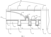
- the light-shielding portion 221 is disposed on the bottom surface of the cover plate 200 in the frame area 130 and configured to change the travel path of the light from the active area 120 and/or adsorb the light from the active area 120, thus avoiding or reducing the light emitting from the through hole 110, thereby improving the photosensitive property of the camera module in the through hole 110 and the display performance of the display panel 100.
- the roughness of the bottom surface of the second region 220 of the cover plate 200 is larger than the roughness of the bottom surface of the first region 210 and larger than the roughness of the third region 230 of the cover plate 200.
- the light-shielding portion 221 is the rough bottom surface of the second region 220. A diffuse reflection occurs when the light from the active area 120 reaches the bottom surface of the second region 220 of the cover plate 200, thus reducing the light leaking from the through hole 110, and improving the photosensitive property of the camera module and the display performance of the display device.
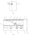
- FIG. 3 is a schematic partial sectional view illustrating the display device taken along a dotted line A-A' in the FIG. 2 .
- the light-interfering layer 300 is disposed on a top surface of the optically clear adhesive layer 131 adjacent to the cover plate 200, and configured to change the travel path of the light from the active area 120 or absorb the light from the active area 120.
- the light-interfering layer 300 may cover the entire top surface of the optically clear adhesive layer 131 or part of the top surface of the optically clear adhesive layer 131.
- the light-interfering layer 300 may be a black gum.
- the light-interfering layer 300 may be a prism or an organic material having a relatively high surface roughness, as long as it may change the travel path of the light from the active area 120 or may absorb the light from the active area.
- the prism may be used to refract light to change the travel path of the light
- the organic material having high surface roughness may be used to form a diffuse reflection of light to change the travel path of the light.
- the organic material having the relatively high surface roughness may be zirconium naphthenate, cobalt naphthenate, nickel naphthenate, titanium naphthenate, or the like.
- the light-interfering layer 300 can be a black gum.
- the black gum is arranged proximate to the active area 120 and surrounding the through hole 110, thereby realizing a better light-blocking effect, effectively preventing the light from leaking from the through hole 110, and moreover, improving the photosensitive property of the camera module and the display performance of the display device.
- FIG. 5 is a schematic partially enlarged view illustrating a sectional structure at the dotted line frame B in the FIG. 4 .
- h1 denotes a height of the light-interfering layer 300 in a direction perpendicular to the display panel 100
- h2 denotes a height of the optically clear adhesive layer 131 disposed at the location corresponding to the light-interfering layer 300, in the direction perpendicular to the display panel 100
- a relationship between the height h1 of the light-interfering layer 300 and the height h2 of the optically clear adhesive layer 131 satisfies: 0.5 ⁇ h 2 ⁇ h 1 ⁇ 0.8 ⁇ h 2 .
- the shielding and blocking effect is unsatisfying, and relatively much light leaks. If the height of the light-interfering layer 300 is too large, for example, larger than 0.8 ⁇ h2 , then a distance between an end of the light-interfering layer 300 and the second inorganic layer 126 is too small, and thus the second inorganic layer 126 tends to be damaged when the optically clear adhesive layer 131 is etched to form the groove.
- the stress at this location may be relatively large, thus causing the display panel 100 to be bent and the second inorganic layer 126 to break easily under an external stress, and affecting the encapsulation effect. Therefore, a reasonable configuration of the height of the light-interfering layer 300 can improve the light-blocking effect of the light-interfering layer 300 while not affecting the encapsulation effect, thereby improving the photosensitive property of the camera module and the display performance of the display device.
- FIG. 6 is a schematic sectional structural view illustrating the display panel provided in an embodiment of the present application.
- the light-interfering layer 300 may be disposed on a surface of the optically clear adhesive layer 131 adjacent to the through hole 110, that is, the light-interfering layer 300 is arranged on and surrounding an inner surface of a side wall of the through hole 110.
- the height of the light-interfering layer 300 in the direction perpendicular to the display panel 100 and the height of the optically clear adhesive layer 131 in the direction perpendicular to the display panel 100 may be identical or different.
- the height of the light-interfering layer 300 in the direction perpendicular to the display panel 100 is the same as the height of the optically clear adhesive layer 131 in the direction perpendicular to the display panel 100, a better light-blocking effect is achieved by the light-interfering layer 300, so that the photosensitive property of the camera module and the display performance of the display panel 100 are significantly improved.
- the light-interfering layer 300 may be any one of the black gum, the prism, and the organic material having a relatively high surface roughness.
- the light-interfering layer 300 can be the black gum.
- the black gum may be formed on an inner side wall of the through hole 110 while the optically clear adhesive layer 131 is being formed.
- a layer of the black gum may be formed on the side wall of the through hole 110 by using a gum-dispensing method after the optically clear adhesive layer 131 is formed.
- a light-interfering layer 300 may be formed in a circle in the third region 230 of the cover plate 200 after the cover plate 200 is formed, and a shape of the light-interfering layer 300 is consistent with a shape of the through hole 110, for example, the light-interfering layer 300 is formed in a circle at a periphery of the third region 230, that is, the light-interfering layer 300 is in a shape of a hollow cylinder.
- the height of the light-interfering layer 300 and the height of the optically clear adhesive layer 131 in the direction perpendicular to the display panel 100 are identical.
- the cover plate 200 After the light-interfering layer 300 is formed on the cover plate 200, the cover plate 200 together with the light-interfering layer 300 is attached onto the display panel 100, where the light-interfering layer 300 is attached onto the inner side wall of the through hole 110, and the components such as front-facing cameral and the handset are arranged in hollow space.
Landscapes
- Physics & Mathematics (AREA)
- Engineering & Computer Science (AREA)
- Optics & Photonics (AREA)
- Microelectronics & Electronic Packaging (AREA)
- Geometry (AREA)
- Devices For Indicating Variable Information By Combining Individual Elements (AREA)
- Theoretical Computer Science (AREA)
- General Physics & Mathematics (AREA)
- Electroluminescent Light Sources (AREA)
- Chemical & Material Sciences (AREA)
- Inorganic Chemistry (AREA)
- Life Sciences & Earth Sciences (AREA)
- Sustainable Development (AREA)
Claims (14)
- Anzeigevorrichtung, umfassend:
ein Anzeigefeld (100), das mit einem Durchgangsloch (110) bereitgestellt ist, das sich in einer Dickenrichtung davon durch das Anzeigefeld (100) erstreckt, und das Anzeigefeld (100) umfassend:einen Rahmenbereich (130), der das Durchgangsloch (110) umgibt; undeinen aktiven Bereich (120), der den Rahmenbereich (130) umgibt; undeine Abdeckplatte (200), die das Anzeigefeld (100) abdeckt, die Abdeckplatte (200) umfassend:einen ersten Bereich (210), der den aktiven Bereich (120) abdeckt;einen zweiten Bereich (220), der den Rahmenbereich (130) abdeckt; undeinen dritten Bereich (230), der das Durchgangsloch (110) abdeckt;dadurch gekennzeichnet, dass:eine Oberfläche des zweiten Bereichs (220) neben dem Anzeigefeld (100) mit einem Lichtabschirmabschnitt (221) bereitgestellt ist, und der Lichtabschirmabschnitt (221) die Oberfläche des zweiten Bereichs (220) neben dem Anzeigefeld (100) umfasst; undeine Rauheit einer Oberfläche des Lichtabschirmabschnitts (221) neben dem Anzeigefeld (100) größer als eine Rauheit einer Oberfläche des ersten Bereichs (210) neben dem Anzeigefeld (100) und größer als eine Rauheit einer Oberfläche des dritten Bereichs (230) neben dem Anzeigefeld (100) ist. - Anzeigevorrichtung nach Anspruch 1, wobei der Lichtabschirmabschnitt (221) eine gesamte Oberfläche des zweiten Bereichs (220) neben dem Anzeigefeld (100) abdeckt.
- Anzeigevorrichtung nach Anspruch 1, wobei ein Substrat (121) in dem Rahmenbereich (130) mit einer Vielzahl von Rillen (134) bereitgestellt ist und ein Vorsprung (136) zwischen benachbarten Rillen (134) bereitgestellt ist.
- Anzeigevorrichtung nach Anspruch 3, wobei eine Lichtemissionsschicht (123) auf den Rillen (134) und auf dem Vorsprung (136) angeordnet ist und die Lichtemissionsschicht (123) zwischen den Rillen (134) und dem Vorsprung (136) unterbrochen ist.
- Anzeigevorrichtung nach Anspruch 1, wobei:der Rahmenbereich (130) ein Substrat (121) umfasst und eine optisch klare Klebeschicht (131) auf dem Substrat (121) angeordnet ist;die Anzeigevorrichtung ferner eine Lichtinterferenzschicht (300) umfasst und die Lichtinterferenzschicht (300) in dem Rahmenbereich (130) angeordnet ist und mit der optisch klaren Klebeschicht (131) in Kontakt steht und konfiguriert ist, um einen seitlichen Lichtaustritt aus dem Durchgangsloch zu verhindern.
- Anzeigevorrichtung nach Anspruch 5, wobei die Lichtinterferenzschicht (300) auf einer Oberfläche der optisch klaren Klebeschicht (130) neben der Abdeckplatte (200) angeordnet ist.
- Anzeigevorrichtung nach Anspruch 6, wobei die Lichtinterferenzschicht (300) eine gesamte Oberfläche der optisch klaren Klebeschicht (130) neben der Abdeckplatte (200) abdeckt.
- Anzeigevorrichtung nach Anspruch 5, wobei die Lichtinterferenzschicht (300) ein beliebiges eines organischen Materials, das eine hohe Oberflächenrauheit aufweist, eines schwarzen Gummis oder eines Prismas umfasst.
- Anzeigevorrichtung nach Anspruch 5, wobei die Lichtinterferenzschicht (300) an einer Seite der optisch klaren Klebeschicht (131) neben dem aktiven Bereich (120) angeordnet ist und mit der Abdeckplatte (200) in Kontakt steht.
- Anzeigevorrichtung nach Anspruch 9, wobeiein Substrat (121) in dem Rahmenbereich (130) mit einer Vielzahl von Rillen (134) bereitgestellt ist und ein Vorsprung (136) zwischen benachbarten Rillen (134) bereitgestellt ist;die Rillen (134) und der Vorsprung (136) nacheinander mit einer Lichtemissionsschicht (123), einer ersten anorganischen Schicht (124) und einer zweiten anorganischen Schicht (126) abgeschieden werden;eine Beziehung zwischen einer Höhe der Lichtinterferenzschicht (300) und einer Höhe der optisch klaren Klebeschicht (131) in einer Richtung senkrecht zu dem Anzeigefeld (100) erfüllt:
 wobei h1 die Höhe der Lichtinterferenzschicht (300) bezeichnet und h2 die Höhe der optisch klaren Klebstoffschicht (131) bezeichnet.
 - Anzeigevorrichtung nach Anspruch 9, wobei das Substrat in dem Rahmenbereich (130) mit einer Vielzahl von Rillen (134) darauf bereitgestellt ist, ein Vorsprung (136) zwischen benachbarten Rillen (134) bereitgestellt ist und sich die Lichtinterferenzschicht (300) über dem Vorsprung (136) befindet.
- Anzeigevorrichtung nach Anspruch 5, wobei die Lichtinterferenzschicht (300) auf der Abdeckplatte (200) ausgebildet ist und die Lichtinterferenzschicht (300) zusammen mit der Abdeckplatte (200) an der Anzeigetafel (100) befestigt ist.
- Anzeigevorrichtung nach Anspruch 1, wobei der Rahmenbereich (130) ein Substrat (121) und eine optisch klare Klebeschicht (131) umfasst, die auf dem Substrat (121) angeordnet ist;
die Anzeigevorrichtung ferner eine Lichtinterferenzschicht (300) umfasst, und sich die Lichtinterferenzschicht (300) umlaufend entlang eines Umfangs des dritten Bereichs (230) der Abdeckplatte (200) erstreckt. - Anzeigevorrichtung nach Anspruch 13, wobei eine Höhe der Lichtinterferenzschicht (300) in einer Richtung senkrecht zu dem Anzeigefeld (100) gleich einer Höhe der optisch klaren Klebeschicht (131) in der Richtung senkrecht zu dem Anzeigefeld (100) ist; und/oder
wobei die Lichtinterferenzschicht (300) in einer Form eines Hohlzylinders ist.
Applications Claiming Priority (2)
| Application Number | Priority Date | Filing Date | Title |
|---|---|---|---|
| CN201911000579.0A CN110634410A (zh) | 2019-10-21 | 2019-10-21 | 显示装置 |
| PCT/CN2020/102795 WO2021077821A1 (zh) | 2019-10-21 | 2020-07-17 | 显示装置 |
Publications (3)
| Publication Number | Publication Date |
|---|---|
| EP3958320A1 EP3958320A1 (de) | 2022-02-23 |
| EP3958320A4 EP3958320A4 (de) | 2022-08-24 |
| EP3958320B1 true EP3958320B1 (de) | 2025-07-02 |
Family
ID=68976951
Family Applications (1)
| Application Number | Title | Priority Date | Filing Date |
|---|---|---|---|
| EP20878636.8A Active EP3958320B1 (de) | 2019-10-21 | 2020-07-17 | Anzeigevorrichtung |
Country Status (6)
| Country | Link |
|---|---|
| US (1) | US12058902B2 (de) |
| EP (1) | EP3958320B1 (de) |
| JP (1) | JP7289935B2 (de) |
| KR (1) | KR102648558B1 (de) |
| CN (1) | CN110634410A (de) |
| WO (1) | WO2021077821A1 (de) |
Families Citing this family (12)
| Publication number | Priority date | Publication date | Assignee | Title |
|---|---|---|---|---|
| CN110634410A (zh) | 2019-10-21 | 2019-12-31 | 昆山国显光电有限公司 | 显示装置 |
| CN111081751B (zh) * | 2020-01-02 | 2023-01-24 | 京东方科技集团股份有限公司 | 一种显示装置及其制作方法 |
| KR102742772B1 (ko) * | 2020-02-13 | 2024-12-13 | 삼성디스플레이 주식회사 | 표시 장치 |
| KR102799087B1 (ko) * | 2020-03-19 | 2025-04-24 | 삼성디스플레이 주식회사 | 표시 장치 |
| KR20220164710A (ko) * | 2020-04-08 | 2022-12-13 | 퀄컴 인코포레이티드 | 디스플레이 패널들의 컷아웃 영역들에 대한 동적 가상 마스크 레이어들 생성 |
| CN111540271B (zh) * | 2020-05-18 | 2022-06-17 | 昆山国显光电有限公司 | 显示面板和显示装置 |
| US11600800B2 (en) * | 2020-07-31 | 2023-03-07 | Innolux Corporation | Electronic device having a curved profile interface corresponding to a recess |
| JP2022072381A (ja) * | 2020-10-29 | 2022-05-17 | 東京エレクトロン株式会社 | 有機elパネルの製造方法及び有機elパネル |
| JP7442419B2 (ja) * | 2020-10-29 | 2024-03-04 | 東京エレクトロン株式会社 | 有機elパネルの製造方法 |
| KR20220082167A (ko) * | 2020-12-09 | 2022-06-17 | 삼성디스플레이 주식회사 | 표시 장치 및 그 제조 방법 |
| CN113888961B (zh) * | 2021-03-05 | 2022-08-12 | 荣耀终端有限公司 | 一种具有折叠屏的电子设备及控制方法 |
| CN113921572B (zh) * | 2021-09-29 | 2025-04-29 | 湖北长江新型显示产业创新中心有限公司 | 显示面板及显示装置 |
Family Cites Families (37)
| Publication number | Priority date | Publication date | Assignee | Title |
|---|---|---|---|---|
| CN100454103C (zh) | 2005-06-01 | 2009-01-21 | 友达光电股份有限公司 | 具防止漏光功能的液晶显示器及其背光模块 |
| JP5298605B2 (ja) * | 2007-04-03 | 2013-09-25 | デクセリアルズ株式会社 | 画像表示装置の製造方法 |
| US8355093B2 (en) | 2010-03-16 | 2013-01-15 | Lg Electronics Inc. | Backlight unit and display device |
| CN102661574B (zh) * | 2012-04-28 | 2014-05-21 | 深圳市华星光电技术有限公司 | 导光板及具有该导光板的背光模组 |
| JP6070026B2 (ja) * | 2012-10-02 | 2017-02-01 | 大日本印刷株式会社 | 有機el表示装置 |
| WO2015033721A1 (ja) * | 2013-09-04 | 2015-03-12 | シャープ株式会社 | 表示パネル |
| KR102248240B1 (ko) * | 2014-02-11 | 2021-05-06 | 삼성디스플레이 주식회사 | 표시장치 및 그 제조방법 |
| KR102524754B1 (ko) | 2015-09-09 | 2023-04-21 | 엘지디스플레이 주식회사 | 표시 장치 |
| KR102421577B1 (ko) * | 2016-04-05 | 2022-07-18 | 삼성디스플레이 주식회사 | 디스플레이 장치 |
| KR102587768B1 (ko) * | 2017-02-24 | 2023-10-12 | 삼성디스플레이 주식회사 | 표시 장치 |
| KR102362598B1 (ko) | 2017-08-08 | 2022-02-14 | 삼성디스플레이 주식회사 | 인쇄회로기판 및 이를 포함하는 표시 장치 |
| JP2019082594A (ja) * | 2017-10-31 | 2019-05-30 | ソニー株式会社 | 表示装置 |
| CN107632453B (zh) * | 2017-10-31 | 2021-03-02 | 京东方科技集团股份有限公司 | 显示面板及制造方法和显示装置 |
| CN207676585U (zh) * | 2017-12-06 | 2018-07-31 | 深圳雷曼光电科技股份有限公司 | Led显示装置 |
| KR102482534B1 (ko) * | 2017-12-19 | 2022-12-28 | 엘지디스플레이 주식회사 | 유기 발광 표시 장치 및 그의 제조방법 |
| KR102527993B1 (ko) | 2018-01-05 | 2023-05-04 | 삼성디스플레이 주식회사 | 표시장치 및 그의 제조방법 |
| KR102520016B1 (ko) | 2018-02-02 | 2023-04-11 | 삼성디스플레이 주식회사 | 표시 패널 및 이를 포함하는 전자 장치 |
| US10620665B2 (en) * | 2018-02-05 | 2020-04-14 | Guangdong Oppo Mobile Telecommunications Corp., Lt | Terminal display assembly and mobile terminal |
| KR102405146B1 (ko) * | 2018-02-08 | 2022-06-08 | 삼성디스플레이 주식회사 | 유기 발광 표시 장치 및 이의 제조 방법 |
| US10991774B2 (en) | 2018-02-12 | 2021-04-27 | Samsung Display Co., Ltd. | Display device and method for fabricating the same |
| CN108919545B (zh) * | 2018-06-28 | 2021-05-04 | 厦门天马微电子有限公司 | 一种显示面板及显示装置 |
| CN108826103B (zh) * | 2018-06-29 | 2020-12-25 | 厦门天马微电子有限公司 | 一种显示装置 |
| CN108845450B (zh) * | 2018-06-29 | 2021-06-04 | Oppo广东移动通信有限公司 | 显示组件和电子设备 |
| CN108957829A (zh) * | 2018-07-06 | 2018-12-07 | Oppo广东移动通信有限公司 | 显示屏组件、电子设备及电子设备的制作方法 |
| CN108681131B (zh) * | 2018-07-27 | 2021-07-30 | 厦门天马微电子有限公司 | 显示装置 |
| CN109031756A (zh) * | 2018-08-01 | 2018-12-18 | 厦门天马微电子有限公司 | 一种显示装置及移动终端 |
| CN109040380B (zh) * | 2018-09-29 | 2024-11-01 | 西安易朴通讯技术有限公司 | 一种显示装置及移动终端 |
| CN208782856U (zh) * | 2018-09-29 | 2019-04-23 | 西安易朴通讯技术有限公司 | 一种显示装置及移动终端 |
| CN109545826B (zh) * | 2018-11-19 | 2020-12-22 | 上海天马微电子有限公司 | 一种显示面板、其制造方法及包含其的显示装置 |
| KR102570864B1 (ko) * | 2018-11-29 | 2023-08-28 | 삼성디스플레이 주식회사 | 전자 장치 |
| KR102763274B1 (ko) * | 2018-11-30 | 2025-02-10 | 삼성디스플레이 주식회사 | 표시장치 |
| US10833292B2 (en) * | 2018-12-20 | 2020-11-10 | Wuhan China Star Optoelectronics Technology Co., Ltd. | Organic light-emitting diode display panel |
| CN109887410B (zh) * | 2019-03-28 | 2021-03-12 | 厦门天马微电子有限公司 | 一种显示装置及显示装置的制作方法 |
| CN110120996B (zh) * | 2019-06-06 | 2021-04-27 | Oppo广东移动通信有限公司 | Oled通孔屏、移动终端、摄像控制方法、装置及存储介质 |
| US20220140040A1 (en) * | 2019-06-28 | 2022-05-05 | Boe Technology Group Co., Ltd. | Display panel, manufacturing method thereof and display device |
| KR102820737B1 (ko) * | 2019-10-02 | 2025-06-16 | 삼성디스플레이 주식회사 | 표시 장치 |
| CN110634410A (zh) * | 2019-10-21 | 2019-12-31 | 昆山国显光电有限公司 | 显示装置 |
-
2019
- 2019-10-21 CN CN201911000579.0A patent/CN110634410A/zh active Pending
-
2020
- 2020-07-17 EP EP20878636.8A patent/EP3958320B1/de active Active
- 2020-07-17 JP JP2021569094A patent/JP7289935B2/ja active Active
- 2020-07-17 WO PCT/CN2020/102795 patent/WO2021077821A1/zh not_active Ceased
- 2020-07-17 KR KR1020217037844A patent/KR102648558B1/ko active Active
-
2021
- 2021-10-18 US US17/504,224 patent/US12058902B2/en active Active
Also Published As
| Publication number | Publication date |
|---|---|
| KR20210148362A (ko) | 2021-12-07 |
| KR102648558B1 (ko) | 2024-03-18 |
| JP2022533229A (ja) | 2022-07-21 |
| CN110634410A (zh) | 2019-12-31 |
| US12058902B2 (en) | 2024-08-06 |
| WO2021077821A1 (zh) | 2021-04-29 |
| EP3958320A1 (de) | 2022-02-23 |
| JP7289935B2 (ja) | 2023-06-12 |
| US20220037442A1 (en) | 2022-02-03 |
| EP3958320A4 (de) | 2022-08-24 |
Similar Documents
| Publication | Publication Date | Title |
|---|---|---|
| US12058902B2 (en) | Display device | |
| CN110853507B (zh) | 一种显示屏和电子设备 | |
| CN111863868B (zh) | 屏下摄像组件及相应的有机发光二极管显示屏和终端设备 | |
| CN107229148B (zh) | 显示屏、显示装置及移动终端 | |
| TWI719738B (zh) | 顯示面板及顯示裝置 | |
| CN108919545B (zh) | 一种显示面板及显示装置 | |
| CN109164648B (zh) | 一种显示面板及显示装置 | |
| EP3522503B1 (de) | Endgeräteanzeigeanordnung und mobiles endgerät | |
| JP4664757B2 (ja) | 液晶表示装置およびその照明装置 | |
| CN110190099B (zh) | 显示面板及显示装置 | |
| CN109887410B (zh) | 一种显示装置及显示装置的制作方法 | |
| EP3832383A1 (de) | Anzeigevorrichtung | |
| US11556024B2 (en) | Display assembly of electronic device, electronic device, and method for manufacturing display assembly | |
| US20200174307A1 (en) | Liquid crystal display device having high screen ratio | |
| CN111613143A (zh) | 显示装置 | |
| EP3690599B1 (de) | Bildschirmrahmen, anzeigebildschirmmodul und endgerät | |
| CN110727147B (zh) | 背光源及电子设备 | |
| US11451651B2 (en) | Display assembly of electronic device and electronic device | |
| US20210356653A1 (en) | Backlight Unit, Method for Manufacturing the Same and Display Device | |
| CN111866220B (zh) | 摄像模组、屏下摄像组件及相应的终端设备 | |
| EP4089988B1 (de) | Endgerätevorrichtung | |
| EP3751340B1 (de) | Mobiles endgerät | |
| WO2015146450A1 (ja) | 液晶表示装置及びテレビ受信装置 | |
| US11419183B2 (en) | Outer frame, terminal housing and terminal | |
| CN110727146B (zh) | 背光源及电子设备 |
Legal Events
| Date | Code | Title | Description |
|---|---|---|---|
| STAA | Information on the status of an ep patent application or granted ep patent |
Free format text: STATUS: THE INTERNATIONAL PUBLICATION HAS BEEN MADE |
|
| PUAI | Public reference made under article 153(3) epc to a published international application that has entered the european phase |
Free format text: ORIGINAL CODE: 0009012 |
|
| STAA | Information on the status of an ep patent application or granted ep patent |
Free format text: STATUS: REQUEST FOR EXAMINATION WAS MADE |
|
| 17P | Request for examination filed |
Effective date: 20211119 |
|
| AK | Designated contracting states |
Kind code of ref document: A1 Designated state(s): AL AT BE BG CH CY CZ DE DK EE ES FI FR GB GR HR HU IE IS IT LI LT LU LV MC MK MT NL NO PL PT RO RS SE SI SK SM TR |
|
| A4 | Supplementary search report drawn up and despatched |
Effective date: 20220721 |
|
| RIC1 | Information provided on ipc code assigned before grant |
Ipc: H01L 51/52 20060101ALI20220715BHEP Ipc: G02F 1/133 20060101ALI20220715BHEP Ipc: G09G 3/32 20160101ALI20220715BHEP Ipc: H01L 27/32 20060101AFI20220715BHEP |
|
| DAV | Request for validation of the european patent (deleted) | ||
| DAX | Request for extension of the european patent (deleted) | ||
| STAA | Information on the status of an ep patent application or granted ep patent |
Free format text: STATUS: EXAMINATION IS IN PROGRESS |
|
| 17Q | First examination report despatched |
Effective date: 20231123 |
|
| REG | Reference to a national code |
Ref country code: DE Ref legal event code: R079 Free format text: PREVIOUS MAIN CLASS: H01L0027320000 Ipc: H10K0059126000 Ref document number: 602020053994 Country of ref document: DE |
|
| GRAP | Despatch of communication of intention to grant a patent |
Free format text: ORIGINAL CODE: EPIDOSNIGR1 |
|
| STAA | Information on the status of an ep patent application or granted ep patent |
Free format text: STATUS: GRANT OF PATENT IS INTENDED |
|
| RIC1 | Information provided on ipc code assigned before grant |
Ipc: H10K 59/80 20230101ALI20250401BHEP Ipc: G02F 1/133 20060101ALI20250401BHEP Ipc: G09G 3/32 20160101ALI20250401BHEP Ipc: H10K 59/126 20230101AFI20250401BHEP |
|
| INTG | Intention to grant announced |
Effective date: 20250414 |
|
| GRAS | Grant fee paid |
Free format text: ORIGINAL CODE: EPIDOSNIGR3 |
|
| GRAA | (expected) grant |
Free format text: ORIGINAL CODE: 0009210 |
|
| STAA | Information on the status of an ep patent application or granted ep patent |
Free format text: STATUS: THE PATENT HAS BEEN GRANTED |
|
| AK | Designated contracting states |
Kind code of ref document: B1 Designated state(s): AL AT BE BG CH CY CZ DE DK EE ES FI FR GB GR HR HU IE IS IT LI LT LU LV MC MK MT NL NO PL PT RO RS SE SI SK SM TR |
|
| REG | Reference to a national code |
Ref country code: GB Ref legal event code: FG4D |
|
| REG | Reference to a national code |
Ref country code: CH Ref legal event code: EP |
|
| REG | Reference to a national code |
Ref country code: DE Ref legal event code: R096 Ref document number: 602020053994 Country of ref document: DE |
|
| REG | Reference to a national code |
Ref country code: IE Ref legal event code: FG4D |
|
| PGFP | Annual fee paid to national office [announced via postgrant information from national office to epo] |
Ref country code: DE Payment date: 20250711 Year of fee payment: 6 |
|
| REG | Reference to a national code |
Ref country code: NL Ref legal event code: MP Effective date: 20250702 |
|
| PG25 | Lapsed in a contracting state [announced via postgrant information from national office to epo] |
Ref country code: PT Free format text: LAPSE BECAUSE OF FAILURE TO SUBMIT A TRANSLATION OF THE DESCRIPTION OR TO PAY THE FEE WITHIN THE PRESCRIBED TIME-LIMIT Effective date: 20251103 |
|
| PG25 | Lapsed in a contracting state [announced via postgrant information from national office to epo] |
Ref country code: NL Free format text: LAPSE BECAUSE OF FAILURE TO SUBMIT A TRANSLATION OF THE DESCRIPTION OR TO PAY THE FEE WITHIN THE PRESCRIBED TIME-LIMIT Effective date: 20250702 |
|
| REG | Reference to a national code |
Ref country code: AT Ref legal event code: MK05 Ref document number: 1810854 Country of ref document: AT Kind code of ref document: T Effective date: 20250702 |
|
| PG25 | Lapsed in a contracting state [announced via postgrant information from national office to epo] |
Ref country code: IS Free format text: LAPSE BECAUSE OF FAILURE TO SUBMIT A TRANSLATION OF THE DESCRIPTION OR TO PAY THE FEE WITHIN THE PRESCRIBED TIME-LIMIT Effective date: 20251102 |
|
| PG25 | Lapsed in a contracting state [announced via postgrant information from national office to epo] |
Ref country code: NO Free format text: LAPSE BECAUSE OF FAILURE TO SUBMIT A TRANSLATION OF THE DESCRIPTION OR TO PAY THE FEE WITHIN THE PRESCRIBED TIME-LIMIT Effective date: 20251002 |
|
| REG | Reference to a national code |
Ref country code: LT Ref legal event code: MG9D |
|
| PG25 | Lapsed in a contracting state [announced via postgrant information from national office to epo] |
Ref country code: AT Free format text: LAPSE BECAUSE OF FAILURE TO SUBMIT A TRANSLATION OF THE DESCRIPTION OR TO PAY THE FEE WITHIN THE PRESCRIBED TIME-LIMIT Effective date: 20250702 |
|
| PG25 | Lapsed in a contracting state [announced via postgrant information from national office to epo] |
Ref country code: FI Free format text: LAPSE BECAUSE OF FAILURE TO SUBMIT A TRANSLATION OF THE DESCRIPTION OR TO PAY THE FEE WITHIN THE PRESCRIBED TIME-LIMIT Effective date: 20250702 |
|
| PG25 | Lapsed in a contracting state [announced via postgrant information from national office to epo] |
Ref country code: HR Free format text: LAPSE BECAUSE OF FAILURE TO SUBMIT A TRANSLATION OF THE DESCRIPTION OR TO PAY THE FEE WITHIN THE PRESCRIBED TIME-LIMIT Effective date: 20250702 |
|
| PG25 | Lapsed in a contracting state [announced via postgrant information from national office to epo] |
Ref country code: GR Free format text: LAPSE BECAUSE OF FAILURE TO SUBMIT A TRANSLATION OF THE DESCRIPTION OR TO PAY THE FEE WITHIN THE PRESCRIBED TIME-LIMIT Effective date: 20251003 |
|
| PG25 | Lapsed in a contracting state [announced via postgrant information from national office to epo] |
Ref country code: SE Free format text: LAPSE BECAUSE OF FAILURE TO SUBMIT A TRANSLATION OF THE DESCRIPTION OR TO PAY THE FEE WITHIN THE PRESCRIBED TIME-LIMIT Effective date: 20250702 Ref country code: CZ Free format text: LAPSE BECAUSE OF FAILURE TO SUBMIT A TRANSLATION OF THE DESCRIPTION OR TO PAY THE FEE WITHIN THE PRESCRIBED TIME-LIMIT Effective date: 20250702 |
|
| PG25 | Lapsed in a contracting state [announced via postgrant information from national office to epo] |
Ref country code: LV Free format text: LAPSE BECAUSE OF FAILURE TO SUBMIT A TRANSLATION OF THE DESCRIPTION OR TO PAY THE FEE WITHIN THE PRESCRIBED TIME-LIMIT Effective date: 20250702 |
|
| PG25 | Lapsed in a contracting state [announced via postgrant information from national office to epo] |
Ref country code: PL Free format text: LAPSE BECAUSE OF FAILURE TO SUBMIT A TRANSLATION OF THE DESCRIPTION OR TO PAY THE FEE WITHIN THE PRESCRIBED TIME-LIMIT Effective date: 20250702 Ref country code: BG Free format text: LAPSE BECAUSE OF FAILURE TO SUBMIT A TRANSLATION OF THE DESCRIPTION OR TO PAY THE FEE WITHIN THE PRESCRIBED TIME-LIMIT Effective date: 20250702 |
|
| PG25 | Lapsed in a contracting state [announced via postgrant information from national office to epo] |
Ref country code: RS Free format text: LAPSE BECAUSE OF FAILURE TO SUBMIT A TRANSLATION OF THE DESCRIPTION OR TO PAY THE FEE WITHIN THE PRESCRIBED TIME-LIMIT Effective date: 20251002 |
|
| PG25 | Lapsed in a contracting state [announced via postgrant information from national office to epo] |
Ref country code: ES Free format text: LAPSE BECAUSE OF FAILURE TO SUBMIT A TRANSLATION OF THE DESCRIPTION OR TO PAY THE FEE WITHIN THE PRESCRIBED TIME-LIMIT Effective date: 20250702 |
|
| REG | Reference to a national code |
Ref country code: CH Ref legal event code: H13 Free format text: ST27 STATUS EVENT CODE: U-0-0-H10-H13 (AS PROVIDED BY THE NATIONAL OFFICE) Effective date: 20260224 |
|
| PG25 | Lapsed in a contracting state [announced via postgrant information from national office to epo] |
Ref country code: RO Free format text: LAPSE BECAUSE OF FAILURE TO SUBMIT A TRANSLATION OF THE DESCRIPTION OR TO PAY THE FEE WITHIN THE PRESCRIBED TIME-LIMIT Effective date: 20250702 Ref country code: LU Free format text: LAPSE BECAUSE OF NON-PAYMENT OF DUE FEES Effective date: 20250717 |
|
| REG | Reference to a national code |
Ref country code: BE Ref legal event code: MM Effective date: 20250731 |
|
| PG25 | Lapsed in a contracting state [announced via postgrant information from national office to epo] |
Ref country code: SM Free format text: LAPSE BECAUSE OF FAILURE TO SUBMIT A TRANSLATION OF THE DESCRIPTION OR TO PAY THE FEE WITHIN THE PRESCRIBED TIME-LIMIT Effective date: 20250702 |
|
| PG25 | Lapsed in a contracting state [announced via postgrant information from national office to epo] |
Ref country code: DK Free format text: LAPSE BECAUSE OF FAILURE TO SUBMIT A TRANSLATION OF THE DESCRIPTION OR TO PAY THE FEE WITHIN THE PRESCRIBED TIME-LIMIT Effective date: 20250702 |
|
| PG25 | Lapsed in a contracting state [announced via postgrant information from national office to epo] |
Ref country code: BE Free format text: LAPSE BECAUSE OF NON-PAYMENT OF DUE FEES Effective date: 20250731 Ref country code: IT Free format text: LAPSE BECAUSE OF FAILURE TO SUBMIT A TRANSLATION OF THE DESCRIPTION OR TO PAY THE FEE WITHIN THE PRESCRIBED TIME-LIMIT Effective date: 20250702 |
|
| PG25 | Lapsed in a contracting state [announced via postgrant information from national office to epo] |
Ref country code: CH Free format text: LAPSE BECAUSE OF NON-PAYMENT OF DUE FEES Effective date: 20250731 |
|
| PG25 | Lapsed in a contracting state [announced via postgrant information from national office to epo] |
Ref country code: SK Free format text: LAPSE BECAUSE OF FAILURE TO SUBMIT A TRANSLATION OF THE DESCRIPTION OR TO PAY THE FEE WITHIN THE PRESCRIBED TIME-LIMIT Effective date: 20250702 Ref country code: EE Free format text: LAPSE BECAUSE OF FAILURE TO SUBMIT A TRANSLATION OF THE DESCRIPTION OR TO PAY THE FEE WITHIN THE PRESCRIBED TIME-LIMIT Effective date: 20250702 |
|
| PLBE | No opposition filed within time limit |
Free format text: ORIGINAL CODE: 0009261 |
|
| STAA | Information on the status of an ep patent application or granted ep patent |
Free format text: STATUS: NO OPPOSITION FILED WITHIN TIME LIMIT |