EP3954677B1 - Neuartige verbindung und diese enthaltende organische lichtemittierende vorrichtung - Google Patents
Neuartige verbindung und diese enthaltende organische lichtemittierende vorrichtung Download PDFInfo
- Publication number
- EP3954677B1 EP3954677B1 EP20844060.2A EP20844060A EP3954677B1 EP 3954677 B1 EP3954677 B1 EP 3954677B1 EP 20844060 A EP20844060 A EP 20844060A EP 3954677 B1 EP3954677 B1 EP 3954677B1
- Authority
- EP
- European Patent Office
- Prior art keywords
- compound
- group
- light emitting
- independently
- stirred
- Prior art date
- Legal status (The legal status is an assumption and is not a legal conclusion. Google has not performed a legal analysis and makes no representation as to the accuracy of the status listed.)
- Active
Links
Images


Classifications
-
- C—CHEMISTRY; METALLURGY
- C07—ORGANIC CHEMISTRY
- C07C—ACYCLIC OR CARBOCYCLIC COMPOUNDS
- C07C211/00—Compounds containing amino groups bound to a carbon skeleton
- C07C211/43—Compounds containing amino groups bound to a carbon skeleton having amino groups bound to carbon atoms of six-membered aromatic rings of the carbon skeleton
- C07C211/57—Compounds containing amino groups bound to a carbon skeleton having amino groups bound to carbon atoms of six-membered aromatic rings of the carbon skeleton having amino groups bound to carbon atoms of six-membered aromatic rings being part of condensed ring systems of the carbon skeleton
- C07C211/61—Compounds containing amino groups bound to a carbon skeleton having amino groups bound to carbon atoms of six-membered aromatic rings of the carbon skeleton having amino groups bound to carbon atoms of six-membered aromatic rings being part of condensed ring systems of the carbon skeleton with at least one of the condensed ring systems formed by three or more rings
-
- C—CHEMISTRY; METALLURGY
- C09—DYES; PAINTS; POLISHES; NATURAL RESINS; ADHESIVES; COMPOSITIONS NOT OTHERWISE PROVIDED FOR; APPLICATIONS OF MATERIALS NOT OTHERWISE PROVIDED FOR
- C09K—MATERIALS FOR MISCELLANEOUS APPLICATIONS, NOT PROVIDED FOR ELSEWHERE
- C09K11/00—Luminescent materials, e.g. electroluminescent or chemiluminescent
- C09K11/06—Luminescent materials, e.g. electroluminescent or chemiluminescent containing organic luminescent materials
-
- H—ELECTRICITY
- H10—SEMICONDUCTOR DEVICES; ELECTRIC SOLID-STATE DEVICES NOT OTHERWISE PROVIDED FOR
- H10K—ORGANIC ELECTRIC SOLID-STATE DEVICES
- H10K85/00—Organic materials used in the body or electrodes of devices covered by this subclass
- H10K85/60—Organic compounds having low molecular weight
- H10K85/615—Polycyclic condensed aromatic hydrocarbons, e.g. anthracene
-
- H—ELECTRICITY
- H10—SEMICONDUCTOR DEVICES; ELECTRIC SOLID-STATE DEVICES NOT OTHERWISE PROVIDED FOR
- H10K—ORGANIC ELECTRIC SOLID-STATE DEVICES
- H10K85/00—Organic materials used in the body or electrodes of devices covered by this subclass
- H10K85/60—Organic compounds having low molecular weight
- H10K85/615—Polycyclic condensed aromatic hydrocarbons, e.g. anthracene
- H10K85/624—Polycyclic condensed aromatic hydrocarbons, e.g. anthracene containing six or more rings
-
- H—ELECTRICITY
- H10—SEMICONDUCTOR DEVICES; ELECTRIC SOLID-STATE DEVICES NOT OTHERWISE PROVIDED FOR
- H10K—ORGANIC ELECTRIC SOLID-STATE DEVICES
- H10K85/00—Organic materials used in the body or electrodes of devices covered by this subclass
- H10K85/60—Organic compounds having low molecular weight
- H10K85/615—Polycyclic condensed aromatic hydrocarbons, e.g. anthracene
- H10K85/626—Polycyclic condensed aromatic hydrocarbons, e.g. anthracene containing more than one polycyclic condensed aromatic rings, e.g. bis-anthracene
-
- H—ELECTRICITY
- H10—SEMICONDUCTOR DEVICES; ELECTRIC SOLID-STATE DEVICES NOT OTHERWISE PROVIDED FOR
- H10K—ORGANIC ELECTRIC SOLID-STATE DEVICES
- H10K85/00—Organic materials used in the body or electrodes of devices covered by this subclass
- H10K85/60—Organic compounds having low molecular weight
- H10K85/631—Amine compounds having at least two aryl rest on at least one amine-nitrogen atom, e.g. triphenylamine
- H10K85/633—Amine compounds having at least two aryl rest on at least one amine-nitrogen atom, e.g. triphenylamine comprising polycyclic condensed aromatic hydrocarbons as substituents on the nitrogen atom
-
- C—CHEMISTRY; METALLURGY
- C07—ORGANIC CHEMISTRY
- C07C—ACYCLIC OR CARBOCYCLIC COMPOUNDS
- C07C2603/00—Systems containing at least three condensed rings
- C07C2603/02—Ortho- or ortho- and peri-condensed systems
- C07C2603/04—Ortho- or ortho- and peri-condensed systems containing three rings
- C07C2603/06—Ortho- or ortho- and peri-condensed systems containing three rings containing at least one ring with less than six ring members
- C07C2603/10—Ortho- or ortho- and peri-condensed systems containing three rings containing at least one ring with less than six ring members containing five-membered rings
- C07C2603/12—Ortho- or ortho- and peri-condensed systems containing three rings containing at least one ring with less than six ring members containing five-membered rings only one five-membered ring
- C07C2603/18—Fluorenes; Hydrogenated fluorenes
-
- C—CHEMISTRY; METALLURGY
- C07—ORGANIC CHEMISTRY
- C07C—ACYCLIC OR CARBOCYCLIC COMPOUNDS
- C07C2603/00—Systems containing at least three condensed rings
- C07C2603/93—Spiro compounds
- C07C2603/94—Spiro compounds containing "free" spiro atoms
-
- C—CHEMISTRY; METALLURGY
- C09—DYES; PAINTS; POLISHES; NATURAL RESINS; ADHESIVES; COMPOSITIONS NOT OTHERWISE PROVIDED FOR; APPLICATIONS OF MATERIALS NOT OTHERWISE PROVIDED FOR
- C09K—MATERIALS FOR MISCELLANEOUS APPLICATIONS, NOT PROVIDED FOR ELSEWHERE
- C09K2211/00—Chemical nature of organic luminescent or tenebrescent compounds
- C09K2211/10—Non-macromolecular compounds
- C09K2211/1003—Carbocyclic compounds
- C09K2211/1014—Carbocyclic compounds bridged by heteroatoms, e.g. N, P, Si or B
-
- H—ELECTRICITY
- H10—SEMICONDUCTOR DEVICES; ELECTRIC SOLID-STATE DEVICES NOT OTHERWISE PROVIDED FOR
- H10K—ORGANIC ELECTRIC SOLID-STATE DEVICES
- H10K50/00—Organic light-emitting devices
- H10K50/10—OLEDs or polymer light-emitting diodes [PLED]
- H10K50/11—OLEDs or polymer light-emitting diodes [PLED] characterised by the electroluminescent [EL] layers
-
- H—ELECTRICITY
- H10—SEMICONDUCTOR DEVICES; ELECTRIC SOLID-STATE DEVICES NOT OTHERWISE PROVIDED FOR
- H10K—ORGANIC ELECTRIC SOLID-STATE DEVICES
- H10K50/00—Organic light-emitting devices
- H10K50/10—OLEDs or polymer light-emitting diodes [PLED]
- H10K50/14—Carrier transporting layers
- H10K50/15—Hole transporting layers
-
- H—ELECTRICITY
- H10—SEMICONDUCTOR DEVICES; ELECTRIC SOLID-STATE DEVICES NOT OTHERWISE PROVIDED FOR
- H10K—ORGANIC ELECTRIC SOLID-STATE DEVICES
- H10K50/00—Organic light-emitting devices
- H10K50/10—OLEDs or polymer light-emitting diodes [PLED]
- H10K50/17—Carrier injection layers
-
- H—ELECTRICITY
- H10—SEMICONDUCTOR DEVICES; ELECTRIC SOLID-STATE DEVICES NOT OTHERWISE PROVIDED FOR
- H10K—ORGANIC ELECTRIC SOLID-STATE DEVICES
- H10K85/00—Organic materials used in the body or electrodes of devices covered by this subclass
- H10K85/30—Coordination compounds
- H10K85/321—Metal complexes comprising a group IIIA element, e.g. Tris (8-hydroxyquinoline) gallium [Gaq3]
- H10K85/322—Metal complexes comprising a group IIIA element, e.g. Tris (8-hydroxyquinoline) gallium [Gaq3] comprising boron
Definitions
- the present disclosure relates to a novel compound and an organic light emitting device comprising the same.
- an organic light emitting phenomenon refers to a phenomenon where electric energy is converted into light energy by using an organic material.
- the organic light emitting device using the organic light emitting phenomenon has characteristics such as a wide viewing angle, an excellent contrast, a fast response time, an excellent luminance, driving voltage and response speed, and thus many studies have proceeded.
- the organic light emitting device generally has a structure which comprises an anode, a cathode, and an organic material layer interposed between the anode and the cathode.
- the organic material layer frequently has a multilayered structure that comprises different materials in order to enhance efficiency and stability of the organic light emitting device, and for example, the organic material layer may be formed of a hole injection layer, a hole transport layer, a light emitting layer, an electron transport layer, an electron injection layer and the like.
- the holes are injected from an anode into the organic material layer and the electrons are injected from the cathode into the organic material layer, and when the injected holes and electrons meet each other, an exciton is formed, and light is emitted when the exciton falls to a ground state again.
- the present disclosure provides novel materials for organic light emitting devices that can be used for an organic light emitting device and simultaneously, can be deposited by a solution process.
- Patent Literature 1 Korean Unexamined Patent Publication No. 10-2000-0051826 KR 10-2018-0092270 A discloses compounds for inclusion in an organic light emitting device.
- an organic light emitting device comprising a first electrode; a second electrode provided opposite the first electrode; and one or more organic material layers provided between the first electrode and the second electrode, wherein one or more of the organic material layers include a cured product of the above-mentioned compound.
- the above-mentioned compound represented by Chemical Formula 1 can be used as a material of an organic material layer of an organic light emitting device, can be used for a solution process, and can improve the efficiency, achieve low driving voltage and/or improve lifetime characteristics in the organic light emitting device.
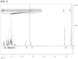
- FIGS. 3 to 7 show NMR data of each compound prepared in Examples of the present disclosure.
- substituted or unsubstituted means being unsubstituted or substituted with one or more substituents selected from the group consisting of deuterium; a halogen group; a cyano group; a nitro group; a hydroxy group; a carbonyl group; an ester group; an imide group; an amino group; a phosphine oxide group; an alkoxy group; an aryloxy group; an alkylthioxy group; an arylthioxy group; an alkylsulfoxy group; an arylsulfoxy group; a silyl group; a boron group; an alkyl group; a cycloalkyl group; an alkenyl group; an aryl group; an aralkyl group; an aralkenyl group; an alkylaryl group; an alkylamine group; an aralkylamine group; a heteroarylamine group; an arylamine group; an arylamine group; an
- a substituent in which two or more substituents are connected may be a biphenyl group.
- a biphenyl group may be an aryl group, or it may also be interpreted as a substituent in which two phenyl groups are connected.
- the carbon number of a carbonyl group is not particularly limited, but is preferably 1 to 40.
- the carbonyl group may be a compound having the following structural formulas, but is not limited thereto.
- an ester group may have a structure in which oxygen of the ester group may be substituted by a straight-chain, branched-chain, or cyclic alkyl group having 1 to 25 carbon atoms, or an aryl group having 6 to 25 carbon atoms.
- the ester group may be a compound having the following structural formulas, but is not limited thereto.
- the carbon number of an imide group is not particularly limited, but is preferably 1 to 25.
- the imide group may be a compound having the following structural formulas, but is not limited thereto.
- a silyl group specifically includes a trimethylsilyl group, a triethylsilyl group, a t-butyldimethylsilyl group, a vinyldimethylsilyl group, a propyldimethylsilyl group, a triphenylsilyl group, a diphenylsilyl group, a phenylsilyl group and the like, but is not limited thereto.
- a boron group specifically includes a trimethylboron group, a triethylboron group, a t-butyldimethylboron group, a triphenylboron group, and a phenylboron group, but is not limited thereto.
- examples of a halogen group include fluorine, chlorine, bromine, or iodine.
- the alkyl group may be straight-chain or branched-chain, and the carbon number thereof is not particularly limited, but is preferably 1 to 40. According to one embodiment, the carbon number of the alkyl group is 1 to 20. According to another embodiment, the carbon number of the alkyl group is 1 to 10. According to another embodiment, the carbon number of the alkyl group is 1 to 6.
- alkyl group examples include methyl, ethyl, propyl, n-propyl, isopropyl, butyl, n-butyl, isobutyl, tert-butyl, sec-butyl, 1-methyl-butyl, 1-ethyl-butyl, pentyl, n-pentyl, isopentyl, neopentyl, tert-pentyl, hexyl, n-hexyl, 1-methylpentyl, 2-methylpentyl, 4-methyl-2-pentyl, 3,3-dimethylbutyl, 2-ethylbutyl, heptyl, n-heptyl, 1-methylhexyl, cyclopentylmethyl, cyclohexylmethyl, octyl, n-octyl, tert-octyl, 1-methylheptyl, 2-ethylhexyl, 2-
- the alkenyl group may be straight-chain or branched-chain, and the carbon number thereof is not particularly limited, but is preferably 2 to 40. According to one embodiment, the carbon number of the alkenyl group is 2 to 20. According to another embodiment, the carbon number of the alkenyl group is 2 to 10. According to still another embodiment, the carbon number of the alkenyl group is 2 to 6.
- Specific examples thereof include vinyl, 1-propenyl, isopropenyl, 1-butenyl, 2-butenyl, 3-butenyl, 1-pentenyl, 2-pentenyl, 3-pentenyl, 3-methyl-1-butenyl, 1,3-butadienyl, allyl, 1-phenylvinyl-1-yl, 2-phenylvinyl-1-yl, 2,2-diphenylvinyl-1-yl, 2-phenyl-2-(naphthyl-1-yl)vinyl-1-yl, 2,2-bis(diphenyl-1-yl)vinyl-1-yl, a stilbenyl group, a styrenyl group, and the like, but are not limited thereto.
- a cycloalkyl group is not particularly limited, but the carbon number thereof is preferably 3 to 60. According to one embodiment, the carbon number of the cycloalkyl group is 3 to 30. According to another embodiment, the carbon number of the cycloalkyl group is 3 to 20. According to still another embodiment, the carbon number of the cycloalkyl group is 3 to 6.
- cyclopropyl examples thereof include cyclopropyl, cyclobutyl, cyclopentyl, 3-methylcyclopentyl, 2,3-dimethylcyclopentyl, cyclohexyl, 3-methylcyclohexyl, 4-methylcyclohexyl, 2,3-dimethylcyclohexyl, 3,4,5-trimethylcyclohexyl, 4-tert-butylcyclohexyl, cycloheptyl, cyclooctyl, and the like, but are not limited thereto.
- an aryl group is not particularly limited, but the carbon number thereof is preferably 6 to 60, and it may be a monocyclic aryl group or a polycyclic aryl group. According to one embodiment, the carbon number of the aryl group is 6 to 30. According to one embodiment, the carbon number of the aryl group is 6 to 20.
- the aryl group may be a phenyl group, a biphenyl group, a terphenyl group or the like as the monocyclic aryl group, but is not limited thereto.
- the polycyclic aryl group includes a naphthyl group, an anthracenyl group, a phenanthrenyl group, a pyrenyl group, a perylenyl group, a chrysenyl group, or the like, but is not limited thereto.
- the fluorenyl group may be substituted, and two substituents may be linked with each other to form a spiro structure.
- the fluorenyl group is substituted, and the like can be formed.
- the structure is not limited thereto.
- a heteroaryl group is a heteroaryl group containing one or more of O, N, Si and S as a heteroatom, and the carbon number thereof is not particularly limited, but is preferably 2 to 60.
- the heteroaryl group include a xanthene group, a thioxanthene group, a thiophene group, a furan group, a pyrrole group, an imidazole group, a thiazole group, an oxazol group, an oxadiazol group, a triazol group, a pyridyl group, a bipyridyl group, a pyrimidyl group, a triazine group, an acridyl group, a pyridazine group, a pyrazinyl group, a quinolinyl group, a quinazoline group, a quinoxalinyl group, a phthalazinyl group, a pyrid
- the aryl group in the aralkyl group, the aralkenyl group, the alkylaryl group, the arylamine group and the arylsily group is the same as the aforementioned examples of the aryl group.
- the alkyl group in the aralkyl group, the alkylaryl group and the alkylamine group is the same as the aforementioned examples of the alkyl group.
- the heteroaryl in the heteroarylamine can be applied to the aforementioned description of the heteroaryl group.
- the alkenyl group in the aralkenyl group is the same as the aforementioned examples of the alkenyl group.
- the aforementioned description of the aryl group may be applied except that the arylene is a divalent group.
- the aforementioned description of the heteroaryl group can be applied except that the heteroarylene is a divalent group.
- the aforementioned description of the aryl group or cycloalkyl group can be applied except that the hydrocarbon ring is not a monovalent group but formed by combining two substituent groups.
- the aforementioned description of the heterocyclic group can be applied, except that the heteroaryl group is not a monovalent group but formed by combining two substituent groups.
- the present disclosure provides a compound represented by Chemical Formula 1 above.
- L is phenylene, biphenyldiyl, or spirobifluorenediyl. More preferably, L is any one selected from the group consisting of:
- L 1 and L 2 are single bonds.
- R 1 is fluoro
- R 2 is hydrogen; deuterium; or methyl.
- Ar 1 and Ar 2 are each independently a substituent group represented by: wherein,
- Ar 1 and Ar 2 are each independently any one selected from the group consisting of:
- Ar 1 and Ar 2 are the same as each other.
- X 1 and X 2 are each independently -L"-R", L" is a single bond, -O-, -S-, -CH 2 -, -CH 2 O-, -OCH 2 -, or -CH 2 OCH 2 -, and R" is any one selected from the group consisting of:
- R' 1 and R" 1 are each independently hydrogen or methyl, and n1 and m1 are each independently an integer of 0 to 2. Also preferably, R' 1 and R" 1 are the same as each other.
- R' 2 , R' 3 , R" 2 and R" 3 are hydrogen.
- step 2 can be omitted.
- the reaction of step 1 and step 2 above is an amine substitution reaction which is preferably carried out in the presence of a palladium catalyst and a base, and a reactive group for the amine substitution reaction can be modified as known in the art.
- the above preparation method may be further embodied in the Preparation Examples described hereinafter.
- the compound according to the present disclosure can form an organic material layer, particularly a hole transport layer, of an organic light emitting device by a solution process.
- a coating composition can be prepared comprising the above-mentioned compound according to the present disclosure and a solvent.
- the solvent is not particularly limited as long as it is a solvent capable of dissolving or dispersing the compound according to the present disclosure.
- the solvent may include chlorine-based solvents such as chloroform, methylene chloride, 1,2-dichloroethane, 1,1,2-trichloroethane, chlorobenzene and o-dichlorobenzene; ether-based solvents such as tetrahydrofuran and dioxane; aromatic hydrocarbon-based solvents such as toluene, xylene, trimethylbenzene and mesitylene; aliphatic hydrocarbon-based solvents such as cyclohexane, methylcyclohexane, n-pentane, n-hexane, n-heptane, n-octane, n-nonane and n-decane; ketone-based solvents such as acetone, methyl ethyl ketone, and cyclohexan
- the viscosity of the coating composition is preferably 1 cP to 10 cP, and coating is easy within the above range. Further, in the coating composition, the concentration of the compound according to the present disclosure is preferably 0.1 wt/v% to 20 wt/v%.
- the coating composition may further include one, two or more types of additives selected from the group consisting of a thermal polymerization initiator and a photopolymerization initiator.
- thermal polymerization initiator may include peroxides such as methyl ethyl ketone peroxide, methyl isobutyl ketone peroxide, acetyl acetone peroxide, methyl cyclohexanone peroxide, cyclohexanone peroxide, isobutyryl peroxide, 2,4-dichlorobenzoyl peroxide, bis-3,5,5-trimethylhexanoyl peroxide, lauryl peroxide, benzoyl peroxide, or azo-based such as azobis isobutylnitrile, azobis dimethylvaleronitrile and azobis cyclohexylnitrile, but are not limited thereto.
- peroxides such as methyl ethyl ketone peroxide, methyl isobutyl ketone peroxide, acetyl acetone peroxide, methyl cyclohexanone peroxide, cyclohexanone
- the photopolymerization initiator may include acetophenone-based or ketal-based photopolymerization initiators such as diethoxyacetophenone, 2,2-dimethoxy-1,2-diphenylethan-1-one, 1-hydroxycyclohexyl-phenyl-ketone, 4-(2-hydroxyethoxy)phenyl-(2-hydroxy-2-propyl)ketone, 2-benzyl-2-dimethylamino-1 -(4-morpholinophenyl)butanone-1,2-hydroxy-2-methyl-1 -phenylpropan-1 -one, 2-methyl-2-morpholino(4-methylthiophenyl)propan-1-one and 1-phenyl-1,2-propanedion-2-(o-ethoxycarbonyl)oxime, benzoin ether-based photopolymerization initiators such as benzoin, benzoin methyl ether, benzoin ethyl ether, benzoin isobutyl ether and benzoin isopropy
- those having a photopolymerization promoting effect can also be used alone or in combination with the photopolymerization initiator.
- examples thereof include triethanolamine, methyldiethanolamine, ethyl 4-dimethylaminobenzoate, isoamyl 4-dimethylamino benzoate, (2-dimethylamino)ethyl benzoate, 4,4'-dimethylaminobenzophenone, and the like, but are not limited thereto.
- a hole transport layer can be produced using the above-mentioned coating composition.
- the method can include the steps of coating the above-mentioned coating composition onto the anode or onto the hole injection layer formed on the anode by a solution process, and heat-treating the coated coating composition.
- the solution process uses the coating composition and refers to spin coating, dip coating, doctor blading, inkjet printing, screen printing, spray method, roll coating, and the like, but is not limited thereto.
- the heat treatment temperature in the heat treatment step is preferably from 150 to 230°C.
- a heat treatment time may be from 1 minute to 3 hours, more preferably 10 minutes to 1 hour.
- the heat treatment is preferably carried out in an inert gas atmosphere such as argon and nitrogen.
- a step of evaporating a solvent may be further included between the coating step and the heat treatment or light treatment step.
- an organic light emitting device comprising a cured product of the compound represented by Chemical Formula 1.
- the organic light emitting device comprises a first electrode; a second electrode that is provided opposite the first electrode; and one or more organic material layers that are provided between the first electrode and the second electrode, wherein one or more of the organic material layers include a cured product of the compound according to the present disclosure.
- the organic light emitting device according to the present disclosure may be a normal type organic light emitting device in which an anode, one or more organic material layers, and a cathode are sequentially stacked on a substrate. Further, the organic light emitting device according to the present disclosure may be an inverted type organic light emitting device in which a cathode, one or more organic material layers, and an anode are sequentially stacked on a substrate. For example, the structure of an organic light emitting device according to an embodiment of the present disclosure is illustrated in FIGS. 1 and 2 .
- FIG. 1 shows an example of an organic light emitting device comprising a substrate 1, an anode 2, a light emitting layer 3, and a cathode 4.
- the compound represented by Chemical Formula 1 may be included in the light emitting layer.
- FIG. 2 shows an example of an organic light emitting device comprising a substrate 1, an anode 2, a hole injection layer 5, a hole transport layer 6, a light emitting layer 7, an electron injection and transport layer 8, and a cathode 4.
- the compound represented by Chemical Formula 1 may be included in the hole injection layer, the hole transport layer, or the light emitting layer.
- the organic light emitting device according to the present disclosure may be manufactured by materials and methods known in the art, except that the light emitting layer includes the compound according to the present disclosure.
- the organic light emitting device can be manufactured by sequentially stacking an anode, an organic material layer and a cathode on a substrate.
- the organic light emitting device may be manufactured by depositing a metal, metal oxides having conductivity, or an alloy thereof on the substrate using a PVD (physical vapor deposition) method such as a sputtering method or an e-beam evaporation method to form an anode, forming organic material layers including the hole injection layer, the hole transport layer, the light emitting layer and the electron transport layer thereon, and then depositing a material that can be used as the cathode thereon.
- PVD physical vapor deposition
- the organic light emitting device may be manufactured by sequentially depositing a cathode material, an organic material layer and an anode material on a substrate (International Publication WO2003/012890 ).
- the manufacturing method is not limited thereto.
- the first electrode is an anode
- the second electrode is a cathode
- the first electrode is a cathode and the second electrode is an anode
- anode material generally, a material having a large work function is preferably used so that holes can be smoothly injected into the organic material layer.
- the anode material include metals such as vanadium, chrome, copper, zinc, and gold, or an alloy thereof; metal oxides such as zinc oxides, indium oxides, indium tin oxides (ITO), and indium zinc oxides (IZO); a combination of metals and oxides, such as ZnO:Al or SnO 2 :Sb; conductive compounds such as poly(3-methylthiophene), poly[3,4-(ethylene-1,2-dioxy)thiophene] (PEDOT), polypyrrole, and polyaniline, and the like, but are not limited thereto.
- the cathode material generally, a material having a small work function is preferably used so that electrons can be easily injected into the organic material layer.
- the cathode material include metals such as magnesium, calcium, sodium, potassium, titanium, indium, yttrium, lithium, gadolinium, aluminum, silver, tin, and lead, or an alloy thereof; a multilayered structure material such as LiF/Al or LiO 2 /Al, and the like, but are not limited thereto.
- the hole injection layer is a layer for injecting holes from the electrode, and the hole injection material is preferably a compound which has a capability of transporting the holes, thus has a hole injecting effect in the anode and an excellent hole injecting effect to the light emitting layer or the light emitting material, prevents excitons produced in the light emitting layer from moving to an electron injection layer or the electron injection material, and further is excellent in the ability to form a thin film. It is preferable that a HOMO (highest occupied molecular orbital) of the hole injection material is between the work function of the anode material and a HOMO of a peripheral organic material layer.
- a HOMO highest occupied molecular orbital
- the hole injection material examples include metal porphyrine, oligothiophene, an arylamine-based organic material, a hexanitrilehexaazatriphenylene-based organic material, a quinacridone-based organic material, a perylene-based organic material, anthraquinone, polyaniline and polythiophene-based conductive compound, and the like, but are not limited thereto.
- the hole transport layer is a layer that receives holes from a hole injection layer and transports the holes to the light emitting layer.
- the hole transport layer is suitably a material having large mobility to the holes, which may receive holes from the anode or the hole injection layer and transfer the holes to the light emitting layer.
- Specific examples thereof include an arylamine-based organic material, a conductive compound, a block copolymer in which a conjugate portion and a non-conjugate portion are present together, and the like, but are not limited thereto.
- the light emitting layer may include a host material and a dopant material.
- the host material may be a fused aromatic ring derivative, a heterocycle-containing compound or the like.
- the fused aromatic ring derivatives include anthracene derivatives, pyrene derivatives, naphthalene derivatives, pentacene derivatives, phenanthrene compounds, and fluoranthene compounds.
- the heterocycle-containing compound include carbazole derivatives, dibenzofuran derivatives, ladder-type furan compounds, pyrimidine derivatives, and the like, but are not limited thereto.
- the dopant material includes an aromatic amine derivative, a styrylamine compound, a boron complex, a fluoranthene compound, a metal complex, or the like.
- the aromatic amine derivative is a fused aromatic ring derivative having a substituted or unsubstituted arylamino group and includes arylamino group-including pyrene, anthracene, chrysene, peryflanthene and the like
- the styrylamine compound is a compound in which substituted or unsubstituted arylamine is substituted with at least one arylvinyl group, and one, two or more substituents selected from the group consisting of an aryl group, a silyl group, an alkyl group, a cycloalkyl group and an arylamino group are substituted or unsubstituted.
- styrylamine styryldiamine, styryltriamine, styryltetramine or the like is included, but the styrylamine compound is not limited thereto.
- the metal complex includes indium complexes, platinum complexes or the like, but is not limited thereto.
- the electron transport layer is a layer which receives electrons from an electron injection layer and transports the electrons to a light emitting layer
- an electron transport material is suitably a material which may receive electrons well from a cathode and transfer the electrons to a light emitting layer, and has a large mobility for electrons.
- Specific examples of the electron transport material include: an Al complex of 8-hydroxyquinoline; a complex including Alq 3 ; an organic radical compound; a hydroxyflavone-metal complex, and the like, but are not limited thereto.
- the electron transport layer may be used with any desired cathode material, as used according to the related art.
- cathode material are a typical material which has a low work function, followed by an aluminum layer or a silver layer.
- specific examples thereof include cesium, barium, calcium, ytterbium, and samarium, in each case followed by an aluminum layer or a silver layer.
- the electron injection layer is a layer which injects electrons from an electrode, and is preferably a compound which has a capability of transporting electrons, has an effect of injecting electrons from a cathode and an excellent effect of injecting electrons into a light emitting layer or a light emitting material, prevents excitons produced from the light emitting layer from moving to a hole injection layer, and is also excellent in the ability to form a thin film.
- the electron injection layer include fluorenone, anthraquinodimethane, diphenoquinone, thiopyran dioxide, oxazole, oxadiazole, triazole, imidazole, perylenetetracarboxylic acid, fluorenylidene methane, anthrone, and the like, and derivatives thereof, a metal complex compound, a nitrogen-containing 5-membered ring derivative, and the like, but are not limited thereto.
- Examples of the metal complex compound include 8-hydroxyquinolinato lithium, bis(8-hydroxyquinolinato)zinc, bis(8-hydroxyquinolinato)copper, bis(8-hydroxyquinolinato)manganese, tris(8-hydroxyquinolinato)aluminum, tris(2-methyl-8-hydroxyquinolinato)aluminum, tris(8-hydroxyquinolinato)gallium, bis(10-hydroxybenzo[h]quinolinato)beryllium, bis(10-hydroxybenzo[h]quinolinato)zinc, bis(2-methyl-8-quinolinato)chlorogallium, bis(2-methyl-8-quinolinato)(o-cresolato)gallium, bis(2-methyl-8-quinolinato)(1-naphtholato)aluminum, bis(2-methyl-8-quinolinato)(2-naphtholato)gallium, and the like, but are not limited thereto.
- the organic light emitting device may be a front side emission type, a back side emission type, or a double side emission type according to the used material.
- the compound according to the present disclosure may be included in an organic solar cell or an organic transistor in addition to an organic light emitting device.
- Methyltriphenyl potassium bromide (13.90 g, 38.91 mmol) and THF (100 mL) were placed in a 250 mL round bottom flask, and stirred at 0°C for 30 minutes.
- n-BuLi(15.6 mL, 38.91 mmol, 2.5 M in hexane) was slowly added to the reaction solution, and stirred at 0°C for 30 minutes.
- 4-Formyl-2,3,5,6-tetrafluoro-1-bromobenzene (5.0 g, 19.47 mmol, 30 mL in THF) was slowly added to the reaction solution at 0°C. The reaction solution was stirred while gradually raising the temperature to room temperature.
- Potassium carbonate (10.4 g, 75.3 mmol) was placed in a 500 mL round bottom flask, to which DMF (200 ml) was added.
- DMF 200 ml
- 2,3,5,6-tetrafluorophenol (10.0 g, 60.22 mmol) was added, and the mixture was stirred at 60°C for 30 minutes.
- 4-Vinylbenzyl chloride (7.66 g, 50.18 mmol) was slowly added to the reaction solution and stirred at 60°C for 16 hours. Then, water (300 mL) and ethyl acetate (200 ml) were added.
- Diiodobiphenyl (5.00 g, 1.0 eq.), NaOtBu(7.10 g, 6.0 eq.), toluene (200 mL), and 3-fluoroaniline (2.39 mL, 2.02 eq.) were placed in a round bottom flask. After nitrogen gassing, the temperature was raised to 90°C. Pd(tBu 3 P) 2 (0.250 g, 4 mol%) was added thereto, and then stirred at 90°C for 1.5 hours. The reaction mixture was worked up by adding ethyl acetate and brine, and then purified by column chromatography to give Compound 4-1.
- Diiodobiphenyl (5.00 g, 1.0 eq.), NaOtBu(7.10 g, 6.0 eq.), toluene (200 mL), and 2-fluoroaniline (2.40 mL, 2.02 eq.) were placed in a round bottom flask. After nitrogen gassing, the temperature was raised to 90°C. Pd(tBu 3 P) 2 (0.250 g, 4 mol%) was added thereto, and then stirred at 90°C for 1 hour. The reaction mixture was worked up by adding ethyl acetate and brine, and then purified by column chromatography to give Compound 5-1.
- Diiodobiphenyl (6.00 g, 1.0 eq.), 2,6-difluoroaniline (4.20 g, 2.2 eq.), NaOtBu (4.26 g, 3.0 eq) and toluene (85 mL) were placed in a round bottom flask. After nitrogen gassing, the temperature was raised to 90°C. Pd(tBu 3 P) 2 was added thereto, and then stirred at 90°C overnight.
- Diiodobiphenyl (4.00 g, 1.0 eq.), 2,4,6-trifluoroaniline (2.2 eq.), NaOtBu (3.79 g, 4.0 eq) and toluene (100 mL) were placed in a round bottom flask. After nitrogen gassing, the temperature was raised to 90°C. Pd(tBu 3 P) 2 (0.25 g, 5 mol%) was added thereto, and then stirred at 90°C overnight. The reaction mixture was worked up by adding ethyl acetate and brine, and then purified by column chromatography to give Compound 10-1.
- Diiodobiphenyl (4.00 g, 1.0 eq.), 3,4,5-trifluoroaniline (2.2 eq.), NaOtBu (3.79 g, 4.0 eq) and toluene (100 mL) were placed in a round bottom flask. After nitrogen gassing, the temperature was raised to 90°C. Pd(tBu 3 P) 2 (0.25 g, 5 mol%) was added thereto, and then stirred at 90°C overnight. The reaction mixture was worked up by adding ethyl acetate and brine, and then purified by column chromatography to give Compound 11-1.
- Diiodobiphenyl (6.00 g, 1.0 eq.), 2,3,4,5,6-pentafluoroaniline (2.2 eq.), NaOtBu (4.26 g, 3.0 eq) and toluene (120 mL) were placed in a round bottom flask. After nitrogen gassing, the temperature was raised to 90°C. Pd(tBu 3 P) 2 (4 mol%) was added thereto, and then stirred at 90°C for 1 hour. The reaction mixture was worked up by adding ethyl acetate and brine, and then purified by column chromatography to give Compound 14-1.
- a glass substrate on which ITO (indium tin oxide) was coated as a thin film to a thickness of 1500 ⁇ was put into distilled water in which a detergent was dissolved, and ultrasonically cleaned.
- a product manufactured by Fischer Co. was used as the detergent, and as the distilled water, distilled water filtered twice using a filter manufactured by Millipore Co. was used.
- ultrasonic cleaning was repeated twice using distilled water for 10 minutes.
- the substrate was ultrasonically cleaned with solvents of isopropyl alcohol and acetone, dried, and then the substrate was cleaned for 5 minutes and then transferred to a glove box.
- a 2 wt% toluene solution of Compound a-NPD below was spin-coated on the hole injection layer and heat-treated at 120°C for 10 minutes to form a hole transport layer having a thickness of 200 ⁇ .
- the deposition rates of the organic materials were maintained at 0.4 to 1.0 ⁇ /sec
- the deposition rates of the LiF and the aluminum of the cathode were maintained at 0.3 ⁇ /sec and 2 ⁇ /sec, respectively
- the degree of vacuum during the deposition was maintained at 2 ⁇ 10 -8 to 5 ⁇ 10 -6 torr.
- the organic light emitting devices were manufactured in the same manner as in Experimental Example 1, except that the compounds shown in Table 1 below were used during the formation of the hole injection layer.
- the organic light emitting devices were manufactured in the same manner as in Experimental Example 1, except that the compounds shown in Table 1 below were used during the formation of the hole injection layer.
- Compounds CE1, CE2, and CE3 in Table 1 are as follows.
- the driving voltage, luminous efficiency, power efficiency, external quantum efficiency (QE), luminance, and color coordinates were measured at a current density of 10 mA/cm 2 , and the results are shown in Table 1 below.
- the external quantum efficiency was determined by (number of photons emitted)/(number of charge carriers injected), and the color coordinates are x and y coordinates based no C.I.E chromaticity diagram (Commission Internationale de L'Eclairage, 1931).
- substrate 2 anode 3: light emitting layer 4: cathode 5: hole injection layer 6: hole transport layer 7: light emitting layer 8: electron injection and transport layer
Landscapes
- Chemical & Material Sciences (AREA)
- Organic Chemistry (AREA)
- Engineering & Computer Science (AREA)
- Materials Engineering (AREA)
- Physics & Mathematics (AREA)
- Spectroscopy & Molecular Physics (AREA)
- Optics & Photonics (AREA)
- Electroluminescent Light Sources (AREA)
- Organic Low-Molecular-Weight Compounds And Preparation Thereof (AREA)
Claims (11)
- Verbindung, dargestellt durch die folgende chemische Formel 1:
 L substituiertes oder unsubstituiertes C6-60-Arylen oder substituiertes oder unsubstituiertes C2-60-Heteroarylen, das irgendeines oder mehrere, aus N, O und S ausgewählte(s) Heteroatom(e) enthält, ist;L1 und L2 jeweils unabhängig eine Einfachbindung oder Methylen sind;X1 und X2 jeweils unabhängig eine fotohärtbare Gruppe oder eine warmhärtende Gruppe sind, unabhängig ausgewählt aus -L"-R", worin L" eine Einfachbindung, -O-, -S-,-CH2-, -CH2O-, -OCH2- oder -CH2OCH2- ist und R" irgendeines der Folgenden ist:

 R'1 bis R'3 und R"1 bis R"3 jeweils unabhängig Wasserstoff, Deuterium, substituiertes oder unsubstituiertes C1-60-Alkyl, substituiertes oder unsubstituiertes C1-60-Alkoxy, substituiertes oder unsubstituiertes C6-60-Aryl oder substituiertes oder unsubstituiertes C2-60-Heteroaryl, enthaltend irgendeines oder mehrere Heteroatome, ausgewählt aus N, O und S, sind;n1 bis n3 und m1 bis m3 jeweils unabhängig eine ganze Zahl von 0 bis 3 sind; undAr1 und Ar2 jeweils unabhängig eine Substituentengruppe sind, dargestellt durch die folgende chemische Formel 2:
 worinjedes R1 unabhängig ein Halogen ist;jedes R2 unabhängig Wasserstoff, Deuterium oder C1-10-Alkyl ist; undn eine ganze Zahl von 1 bis 5 ist und m 0 oder 1 ist, vorausgesetzt, dass m+n 5 oder kleiner ist.
 - Verbindung gemäß Anspruch 1, worin L Phenylen, Biphenyldiyl oder Spirobifluorendiyl ist.
- Verbindung gemäß Anspruch 1, worin L irgendeines der Folgenden ist:

- Verbindung gemäß Anspruch 1, worin R1 Fluor ist.
- Verbindung gemäß Anspruch 1, worin R2 Wasserstoff, Deuterium oder Methyl ist.
- Verbindung gemäß Anspruch 1, worin Ar1 und Ar2 jeweils unabhängig eine Substituentengruppe sind, dargestellt durch:
 R1 C1-10-Alkyl oder ein Halogen ist; undR2 Wasserstoff, Deuterium, C1-10-Alkyl oder ein Halogen ist;vorausgesetzt, dass zumindest eines von R1 und R2 ein Halogen ist.
 - Verbindung gemäß Anspruch 1, worin Ar1 und Ar2 jeweils unabhängig irgendeines der Folgenden sind:


- Verbindung gemäß Anspruch 1, worinR'1 und R"1 jeweils unabhängig Wasserstoff oder Methyl sind; undn1 und m1 jeweils unabhängig eine ganze Zahl von 0 bis 2 sind.
- Verbindung gemäß Anspruch 1, worin R'2, R'3, R"2 und R"3 Wasserstoff sind.
- Verbindung gemäß Anspruch 1, die irgendeine der Folgenden ist:


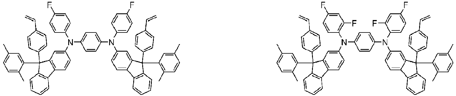


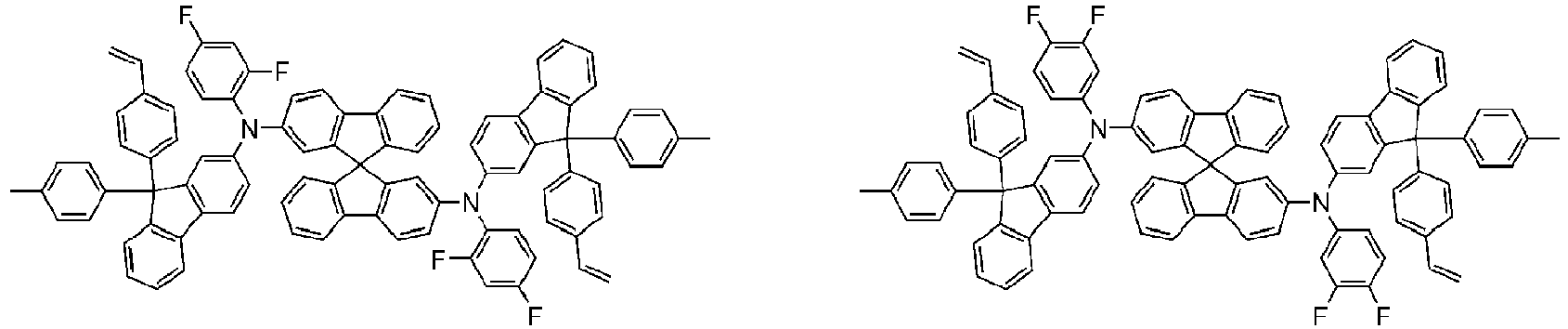


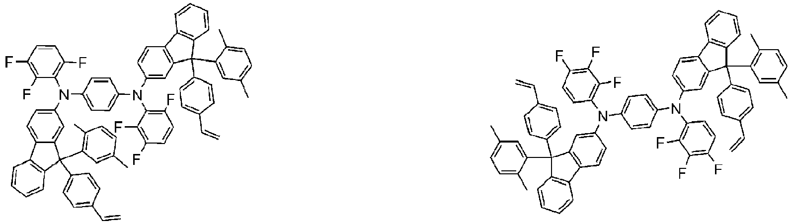


- Organische lichtemittierende Vorrichtung, umfassend:eine erste Elektrode;eine zweite Elektrode, die gegenüberliegend zur ersten Elektrode vorgesehen ist; undeine oder mehr organische Materialschicht(en), vorgesehen zwischen der ersten Elektrode und der zweiten Elektrode, worin eine oder mehr der organischen Materialschicht(en) ein gehärtetes Produkt der Verbindung gemäß irgendeinem der Ansprüche 1 bis 10 umfasst.
Applications Claiming Priority (2)
| Application Number | Priority Date | Filing Date | Title |
|---|---|---|---|
| KR20190089701 | 2019-07-24 | ||
| PCT/KR2020/009556 WO2021015522A1 (ko) | 2019-07-24 | 2020-07-20 | 신규한 화합물 및 이를 이용한 유기 발광 소자 |
Publications (3)
| Publication Number | Publication Date |
|---|---|
| EP3954677A1 EP3954677A1 (de) | 2022-02-16 |
| EP3954677A4 EP3954677A4 (de) | 2022-06-15 |
| EP3954677B1 true EP3954677B1 (de) | 2024-10-23 |
Family
ID=74192644
Family Applications (1)
| Application Number | Title | Priority Date | Filing Date |
|---|---|---|---|
| EP20844060.2A Active EP3954677B1 (de) | 2019-07-24 | 2020-07-20 | Neuartige verbindung und diese enthaltende organische lichtemittierende vorrichtung |
Country Status (7)
| Country | Link |
|---|---|
| US (1) | US20220064101A1 (de) |
| EP (1) | EP3954677B1 (de) |
| JP (1) | JP7334886B2 (de) |
| KR (2) | KR102561761B1 (de) |
| CN (1) | CN113795477B (de) |
| TW (1) | TWI785353B (de) |
| WO (1) | WO2021015522A1 (de) |
Families Citing this family (2)
| Publication number | Priority date | Publication date | Assignee | Title |
|---|---|---|---|---|
| US20250228128A1 (en) * | 2022-09-23 | 2025-07-10 | Lg Chem, Ltd. | Ink Composition, Organic Material Layer Comprising Same, and Organic Light-Emitting Device Comprising Same |
| WO2024096610A1 (ko) * | 2022-11-04 | 2024-05-10 | 주식회사 엘지화학 | 잉크 조성물, 이를 포함하는 유기물층 및 이를 포함하는 유기 발광 소자 |
Family Cites Families (13)
| Publication number | Priority date | Publication date | Assignee | Title |
|---|---|---|---|---|
| KR100430549B1 (ko) | 1999-01-27 | 2004-05-10 | 주식회사 엘지화학 | 신규한 착물 및 그의 제조 방법과 이를 이용한 유기 발광 소자 및 그의 제조 방법 |
| DE10135513B4 (de) | 2001-07-20 | 2005-02-24 | Novaled Gmbh | Lichtemittierendes Bauelement mit organischen Schichten |
| JP3848307B2 (ja) * | 2003-06-27 | 2006-11-22 | キヤノン株式会社 | アミノアントリル誘導基置換化合物およびそれを使用した有機発光素子 |
| KR101513727B1 (ko) * | 2007-06-20 | 2015-04-20 | 에스케이이노베이션 주식회사 | 불소기를 포함하는 전기발광고분자 및 이를 이용한전기발광소자 |
| EP2610240A1 (de) | 2011-12-28 | 2013-07-03 | Solvay Sa | Vernetzbare Arylamin-Verbindungen |
| KR102109353B1 (ko) * | 2013-05-08 | 2020-05-12 | 덕산네오룩스 주식회사 | 유기전기 소자용 화합물, 이를 이용한 유기전기소자 및 그 전자 장치 |
| KR102117603B1 (ko) * | 2014-02-10 | 2020-06-01 | 덕산네오룩스 주식회사 | 유기전기소자용 화합물, 이를 이용한 유기전기소자 및 그 전자 장치 |
| WO2017100967A1 (zh) * | 2015-12-14 | 2017-06-22 | 武汉尚赛光电科技有限公司 | 具有电子供体-受体结构的苯并[c]菲类的衍生物、其应用及电致发光器件 |
| KR102654996B1 (ko) * | 2016-10-06 | 2024-04-05 | 메르크 파텐트 게엠베하 | 유기 전계발광 소자용 재료 |
| JP6820055B2 (ja) * | 2017-02-28 | 2021-01-27 | エルジー・ケム・リミテッド | フルオレン系化合物、これを用いた有機発光素子およびその製造方法 |
| KR102072917B1 (ko) * | 2017-09-26 | 2020-03-02 | 주식회사 엘지화학 | 코팅 조성물, 이를 이용한 유기 발광 소자 및 이의 제조방법 |
| KR102430143B1 (ko) | 2018-05-30 | 2022-08-08 | 주식회사 엘지화학 | 코팅 조성물, 이를 이용한 유기 발광 소자 및 이의 제조방법 |
| KR102217266B1 (ko) | 2018-09-28 | 2021-02-17 | 주식회사 엘지화학 | 유기 발광 소자용 잉크 조성물 |
-
2020
- 2020-07-20 US US17/610,331 patent/US20220064101A1/en not_active Abandoned
- 2020-07-20 KR KR1020200089652A patent/KR102561761B1/ko active Active
- 2020-07-20 CN CN202080032703.6A patent/CN113795477B/zh active Active
- 2020-07-20 EP EP20844060.2A patent/EP3954677B1/de active Active
- 2020-07-20 WO PCT/KR2020/009556 patent/WO2021015522A1/ko not_active Ceased
- 2020-07-20 JP JP2021564601A patent/JP7334886B2/ja active Active
- 2020-07-23 TW TW109124861A patent/TWI785353B/zh active
- 2020-07-24 KR KR1020200092537A patent/KR102914098B1/ko active Active
Also Published As
| Publication number | Publication date |
|---|---|
| CN113795477A (zh) | 2021-12-14 |
| EP3954677A1 (de) | 2022-02-16 |
| JP2022530974A (ja) | 2022-07-05 |
| KR20210012936A (ko) | 2021-02-03 |
| KR102561761B1 (ko) | 2023-07-31 |
| KR20210012972A (ko) | 2021-02-03 |
| JP7334886B2 (ja) | 2023-08-29 |
| KR102914098B1 (ko) | 2026-01-19 |
| WO2021015522A1 (ko) | 2021-01-28 |
| TW202110790A (zh) | 2021-03-16 |
| TWI785353B (zh) | 2022-12-01 |
| CN113795477B (zh) | 2023-12-12 |
| US20220064101A1 (en) | 2022-03-03 |
| EP3954677A4 (de) | 2022-06-15 |
Similar Documents
| Publication | Publication Date | Title |
|---|---|---|
| EP4230629B1 (de) | Neuartige verbindung und organische lichtemittierende vorrichtung damit | |
| EP4227312B1 (de) | Neuartige verbindung und organische lichtemittierende vorrichtung damit | |
| EP4230630B1 (de) | Neuartige verbindung und diese enthaltende organische lichtemittierende vorrichtung | |
| EP4071193B1 (de) | Neuartiges polymer und organisches lichtemittierendes element damit | |
| KR102670481B1 (ko) | 유기 발광 소자 | |
| EP3699231B1 (de) | Neuartiges polymer und organische lichtemittierende vorrichtung damit | |
| EP3954677B1 (de) | Neuartige verbindung und diese enthaltende organische lichtemittierende vorrichtung | |
| EP4265625A1 (de) | Neuartige verbindung und organische lichtemittierende vorrichtung damit | |
| EP4145546B1 (de) | Organische lichtemittierende vorrichtung | |
| EP4092035B1 (de) | Neuartige verbindung und organische lichtemittierende vorrichtung damit | |
| EP4293030A1 (de) | Neuartige verbindung und organische lichtemittierende vorrichtung damit | |
| EP4063367B1 (de) | Neuartige verbindung und organische lichtemittierende vorrichtung mit verwendung davon | |
| KR20200029344A (ko) | 신규한 화합물 및 이를 포함하는 유기 발광 소자 | |
| CN112638956B (zh) | 聚合物和包含其的有机发光器件 | |
| EP4092033A1 (de) | Neuartige verbindung und organische lichtemittierende vorrichtung mit verwendung davon | |
| EP4245760B1 (de) | Neuartige verbindung und organische lichtemittierende vorrichtung damit | |
| EP4279492B1 (de) | Neuartige verbindung und organische lichtemittierende vorrichtung damit | |
| EP4335854A1 (de) | Neuartige verbindung und organische lichtemittierende vorrichtung damit | |
| EP4279493A1 (de) | Neuartige verbindung und organische lichtemittierende vorrichtung damit | |
| KR102734119B1 (ko) | 유기 발광 소자 | |
| KR20220036733A (ko) | 유기 발광 소자 |
Legal Events
| Date | Code | Title | Description |
|---|---|---|---|
| STAA | Information on the status of an ep patent application or granted ep patent |
Free format text: STATUS: THE INTERNATIONAL PUBLICATION HAS BEEN MADE |
|
| PUAI | Public reference made under article 153(3) epc to a published international application that has entered the european phase |
Free format text: ORIGINAL CODE: 0009012 |
|
| STAA | Information on the status of an ep patent application or granted ep patent |
Free format text: STATUS: REQUEST FOR EXAMINATION WAS MADE |
|
| 17P | Request for examination filed |
Effective date: 20211111 |
|
| AK | Designated contracting states |
Kind code of ref document: A1 Designated state(s): AL AT BE BG CH CY CZ DE DK EE ES FI FR GB GR HR HU IE IS IT LI LT LU LV MC MK MT NL NO PL PT RO RS SE SI SK SM TR |
|
| A4 | Supplementary search report drawn up and despatched |
Effective date: 20220516 |
|
| RIC1 | Information provided on ipc code assigned before grant |
Ipc: C09K 11/06 20060101ALI20220510BHEP Ipc: H01L 51/50 20060101ALI20220510BHEP Ipc: H01L 51/00 20060101ALI20220510BHEP Ipc: C07C 211/61 20060101AFI20220510BHEP |
|
| DAV | Request for validation of the european patent (deleted) | ||
| DAX | Request for extension of the european patent (deleted) | ||
| STAA | Information on the status of an ep patent application or granted ep patent |
Free format text: STATUS: EXAMINATION IS IN PROGRESS |
|
| 17Q | First examination report despatched |
Effective date: 20231128 |
|
| GRAP | Despatch of communication of intention to grant a patent |
Free format text: ORIGINAL CODE: EPIDOSNIGR1 |
|
| STAA | Information on the status of an ep patent application or granted ep patent |
Free format text: STATUS: GRANT OF PATENT IS INTENDED |
|
| RIC1 | Information provided on ipc code assigned before grant |
Ipc: C09K 11/06 20060101ALI20240618BHEP Ipc: C07C 211/61 20060101AFI20240618BHEP |
|
| INTG | Intention to grant announced |
Effective date: 20240715 |
|
| GRAS | Grant fee paid |
Free format text: ORIGINAL CODE: EPIDOSNIGR3 |
|
| GRAA | (expected) grant |
Free format text: ORIGINAL CODE: 0009210 |
|
| STAA | Information on the status of an ep patent application or granted ep patent |
Free format text: STATUS: THE PATENT HAS BEEN GRANTED |
|
| AK | Designated contracting states |
Kind code of ref document: B1 Designated state(s): AL AT BE BG CH CY CZ DE DK EE ES FI FR GB GR HR HU IE IS IT LI LT LU LV MC MK MT NL NO PL PT RO RS SE SI SK SM TR |
|
| REG | Reference to a national code |
Ref country code: GB Ref legal event code: FG4D |
|
| REG | Reference to a national code |
Ref country code: CH Ref legal event code: EP |
|
| REG | Reference to a national code |
Ref country code: DE Ref legal event code: R096 Ref document number: 602020040038 Country of ref document: DE |
|
| REG | Reference to a national code |
Ref country code: IE Ref legal event code: FG4D |
|
| REG | Reference to a national code |
Ref country code: LT Ref legal event code: MG9D |
|
| REG | Reference to a national code |
Ref country code: NL Ref legal event code: MP Effective date: 20241023 |
|
| REG | Reference to a national code |
Ref country code: AT Ref legal event code: MK05 Ref document number: 1734748 Country of ref document: AT Kind code of ref document: T Effective date: 20241023 |
|
| PG25 | Lapsed in a contracting state [announced via postgrant information from national office to epo] |
Ref country code: NL Free format text: LAPSE BECAUSE OF FAILURE TO SUBMIT A TRANSLATION OF THE DESCRIPTION OR TO PAY THE FEE WITHIN THE PRESCRIBED TIME-LIMIT Effective date: 20241023 |
|
| PG25 | Lapsed in a contracting state [announced via postgrant information from national office to epo] |
Ref country code: NL Free format text: LAPSE BECAUSE OF FAILURE TO SUBMIT A TRANSLATION OF THE DESCRIPTION OR TO PAY THE FEE WITHIN THE PRESCRIBED TIME-LIMIT Effective date: 20241023 |
|
| PG25 | Lapsed in a contracting state [announced via postgrant information from national office to epo] |
Ref country code: PT Free format text: LAPSE BECAUSE OF FAILURE TO SUBMIT A TRANSLATION OF THE DESCRIPTION OR TO PAY THE FEE WITHIN THE PRESCRIBED TIME-LIMIT Effective date: 20250224 Ref country code: IS Free format text: LAPSE BECAUSE OF FAILURE TO SUBMIT A TRANSLATION OF THE DESCRIPTION OR TO PAY THE FEE WITHIN THE PRESCRIBED TIME-LIMIT Effective date: 20250223 Ref country code: HR Free format text: LAPSE BECAUSE OF FAILURE TO SUBMIT A TRANSLATION OF THE DESCRIPTION OR TO PAY THE FEE WITHIN THE PRESCRIBED TIME-LIMIT Effective date: 20241023 |
|
| PG25 | Lapsed in a contracting state [announced via postgrant information from national office to epo] |
Ref country code: FI Free format text: LAPSE BECAUSE OF FAILURE TO SUBMIT A TRANSLATION OF THE DESCRIPTION OR TO PAY THE FEE WITHIN THE PRESCRIBED TIME-LIMIT Effective date: 20241023 |
|
| PG25 | Lapsed in a contracting state [announced via postgrant information from national office to epo] |
Ref country code: BG Free format text: LAPSE BECAUSE OF FAILURE TO SUBMIT A TRANSLATION OF THE DESCRIPTION OR TO PAY THE FEE WITHIN THE PRESCRIBED TIME-LIMIT Effective date: 20241023 |
|
| PG25 | Lapsed in a contracting state [announced via postgrant information from national office to epo] |
Ref country code: ES Free format text: LAPSE BECAUSE OF FAILURE TO SUBMIT A TRANSLATION OF THE DESCRIPTION OR TO PAY THE FEE WITHIN THE PRESCRIBED TIME-LIMIT Effective date: 20241023 |
|
| PG25 | Lapsed in a contracting state [announced via postgrant information from national office to epo] |
Ref country code: NO Free format text: LAPSE BECAUSE OF FAILURE TO SUBMIT A TRANSLATION OF THE DESCRIPTION OR TO PAY THE FEE WITHIN THE PRESCRIBED TIME-LIMIT Effective date: 20250123 |
|
| PG25 | Lapsed in a contracting state [announced via postgrant information from national office to epo] |
Ref country code: AT Free format text: LAPSE BECAUSE OF FAILURE TO SUBMIT A TRANSLATION OF THE DESCRIPTION OR TO PAY THE FEE WITHIN THE PRESCRIBED TIME-LIMIT Effective date: 20241023 Ref country code: LV Free format text: LAPSE BECAUSE OF FAILURE TO SUBMIT A TRANSLATION OF THE DESCRIPTION OR TO PAY THE FEE WITHIN THE PRESCRIBED TIME-LIMIT Effective date: 20241023 Ref country code: GR Free format text: LAPSE BECAUSE OF FAILURE TO SUBMIT A TRANSLATION OF THE DESCRIPTION OR TO PAY THE FEE WITHIN THE PRESCRIBED TIME-LIMIT Effective date: 20250124 |
|
| PG25 | Lapsed in a contracting state [announced via postgrant information from national office to epo] |
Ref country code: PL Free format text: LAPSE BECAUSE OF FAILURE TO SUBMIT A TRANSLATION OF THE DESCRIPTION OR TO PAY THE FEE WITHIN THE PRESCRIBED TIME-LIMIT Effective date: 20241023 |
|
| PG25 | Lapsed in a contracting state [announced via postgrant information from national office to epo] |
Ref country code: RS Free format text: LAPSE BECAUSE OF FAILURE TO SUBMIT A TRANSLATION OF THE DESCRIPTION OR TO PAY THE FEE WITHIN THE PRESCRIBED TIME-LIMIT Effective date: 20250123 |
|
| PG25 | Lapsed in a contracting state [announced via postgrant information from national office to epo] |
Ref country code: SM Free format text: LAPSE BECAUSE OF FAILURE TO SUBMIT A TRANSLATION OF THE DESCRIPTION OR TO PAY THE FEE WITHIN THE PRESCRIBED TIME-LIMIT Effective date: 20241023 |
|
| PG25 | Lapsed in a contracting state [announced via postgrant information from national office to epo] |
Ref country code: DK Free format text: LAPSE BECAUSE OF FAILURE TO SUBMIT A TRANSLATION OF THE DESCRIPTION OR TO PAY THE FEE WITHIN THE PRESCRIBED TIME-LIMIT Effective date: 20241023 |
|
| PG25 | Lapsed in a contracting state [announced via postgrant information from national office to epo] |
Ref country code: EE Free format text: LAPSE BECAUSE OF FAILURE TO SUBMIT A TRANSLATION OF THE DESCRIPTION OR TO PAY THE FEE WITHIN THE PRESCRIBED TIME-LIMIT Effective date: 20241023 |
|
| PGFP | Annual fee paid to national office [announced via postgrant information from national office to epo] |
Ref country code: FR Payment date: 20250624 Year of fee payment: 6 |
|
| PG25 | Lapsed in a contracting state [announced via postgrant information from national office to epo] |
Ref country code: RO Free format text: LAPSE BECAUSE OF FAILURE TO SUBMIT A TRANSLATION OF THE DESCRIPTION OR TO PAY THE FEE WITHIN THE PRESCRIBED TIME-LIMIT Effective date: 20241023 |
|
| REG | Reference to a national code |
Ref country code: DE Ref legal event code: R097 Ref document number: 602020040038 Country of ref document: DE |
|
| PG25 | Lapsed in a contracting state [announced via postgrant information from national office to epo] |
Ref country code: SK Free format text: LAPSE BECAUSE OF FAILURE TO SUBMIT A TRANSLATION OF THE DESCRIPTION OR TO PAY THE FEE WITHIN THE PRESCRIBED TIME-LIMIT Effective date: 20241023 |
|
| PG25 | Lapsed in a contracting state [announced via postgrant information from national office to epo] |
Ref country code: CZ Free format text: LAPSE BECAUSE OF FAILURE TO SUBMIT A TRANSLATION OF THE DESCRIPTION OR TO PAY THE FEE WITHIN THE PRESCRIBED TIME-LIMIT Effective date: 20241023 |
|
| PG25 | Lapsed in a contracting state [announced via postgrant information from national office to epo] |
Ref country code: IT Free format text: LAPSE BECAUSE OF FAILURE TO SUBMIT A TRANSLATION OF THE DESCRIPTION OR TO PAY THE FEE WITHIN THE PRESCRIBED TIME-LIMIT Effective date: 20241023 |
|
| PLBE | No opposition filed within time limit |
Free format text: ORIGINAL CODE: 0009261 |
|
| STAA | Information on the status of an ep patent application or granted ep patent |
Free format text: STATUS: NO OPPOSITION FILED WITHIN TIME LIMIT |
|
| PG25 | Lapsed in a contracting state [announced via postgrant information from national office to epo] |
Ref country code: SE Free format text: LAPSE BECAUSE OF FAILURE TO SUBMIT A TRANSLATION OF THE DESCRIPTION OR TO PAY THE FEE WITHIN THE PRESCRIBED TIME-LIMIT Effective date: 20241023 |
|
| 26N | No opposition filed |
Effective date: 20250724 |
|
| PGFP | Annual fee paid to national office [announced via postgrant information from national office to epo] |
Ref country code: DE Payment date: 20250624 Year of fee payment: 6 |
|
| REG | Reference to a national code |
Ref country code: CH Ref legal event code: H13 Free format text: ST27 STATUS EVENT CODE: U-0-0-H10-H13 (AS PROVIDED BY THE NATIONAL OFFICE) Effective date: 20260224 |
|
| PG25 | Lapsed in a contracting state [announced via postgrant information from national office to epo] |
Ref country code: LU Free format text: LAPSE BECAUSE OF NON-PAYMENT OF DUE FEES Effective date: 20250720 |
|
| GBPC | Gb: european patent ceased through non-payment of renewal fee |
Effective date: 20250720 |
|
| REG | Reference to a national code |
Ref country code: BE Ref legal event code: MM Effective date: 20250731 |
|
| PG25 | Lapsed in a contracting state [announced via postgrant information from national office to epo] |
Ref country code: GB Free format text: LAPSE BECAUSE OF NON-PAYMENT OF DUE FEES Effective date: 20250720 |
|
| PG25 | Lapsed in a contracting state [announced via postgrant information from national office to epo] |
Ref country code: BE Free format text: LAPSE BECAUSE OF NON-PAYMENT OF DUE FEES Effective date: 20250731 |
|
| PG25 | Lapsed in a contracting state [announced via postgrant information from national office to epo] |
Ref country code: CH Free format text: LAPSE BECAUSE OF NON-PAYMENT OF DUE FEES Effective date: 20250731 |