EP4227312B1 - Neuartige verbindung und organische lichtemittierende vorrichtung damit - Google Patents
Neuartige verbindung und organische lichtemittierende vorrichtung damit Download PDFInfo
- Publication number
- EP4227312B1 EP4227312B1 EP21915573.6A EP21915573A EP4227312B1 EP 4227312 B1 EP4227312 B1 EP 4227312B1 EP 21915573 A EP21915573 A EP 21915573A EP 4227312 B1 EP4227312 B1 EP 4227312B1
- Authority
- EP
- European Patent Office
- Prior art keywords
- compound
- group
- light emitting
- substituted
- unsubstituted
- Prior art date
- Legal status (The legal status is an assumption and is not a legal conclusion. Google has not performed a legal analysis and makes no representation as to the accuracy of the status listed.)
- Active
Links
Images
Classifications
-
- C—CHEMISTRY; METALLURGY
- C07—ORGANIC CHEMISTRY
- C07F—ACYCLIC, CARBOCYCLIC OR HETEROCYCLIC COMPOUNDS CONTAINING ELEMENTS OTHER THAN CARBON, HYDROGEN, HALOGEN, OXYGEN, NITROGEN, SULFUR, SELENIUM OR TELLURIUM
- C07F5/00—Compounds containing elements of Groups 3 or 13 of the Periodic Table
- C07F5/02—Boron compounds
- C07F5/027—Organoboranes and organoborohydrides
-
- C—CHEMISTRY; METALLURGY
- C09—DYES; PAINTS; POLISHES; NATURAL RESINS; ADHESIVES; COMPOSITIONS NOT OTHERWISE PROVIDED FOR; APPLICATIONS OF MATERIALS NOT OTHERWISE PROVIDED FOR
- C09K—MATERIALS FOR MISCELLANEOUS APPLICATIONS, NOT PROVIDED FOR ELSEWHERE
- C09K11/00—Luminescent materials, e.g. electroluminescent or chemiluminescent
- C09K11/06—Luminescent materials, e.g. electroluminescent or chemiluminescent containing organic luminescent materials
-
- H—ELECTRICITY
- H10—SEMICONDUCTOR DEVICES; ELECTRIC SOLID-STATE DEVICES NOT OTHERWISE PROVIDED FOR
- H10K—ORGANIC ELECTRIC SOLID-STATE DEVICES
- H10K50/00—Organic light-emitting devices
- H10K50/10—OLEDs or polymer light-emitting diodes [PLED]
- H10K50/11—OLEDs or polymer light-emitting diodes [PLED] characterised by the electroluminescent [EL] layers
- H10K50/12—OLEDs or polymer light-emitting diodes [PLED] characterised by the electroluminescent [EL] layers comprising dopants
-
- H—ELECTRICITY
- H10—SEMICONDUCTOR DEVICES; ELECTRIC SOLID-STATE DEVICES NOT OTHERWISE PROVIDED FOR
- H10K—ORGANIC ELECTRIC SOLID-STATE DEVICES
- H10K85/00—Organic materials used in the body or electrodes of devices covered by this subclass
- H10K85/60—Organic compounds having low molecular weight
- H10K85/615—Polycyclic condensed aromatic hydrocarbons, e.g. anthracene
- H10K85/622—Polycyclic condensed aromatic hydrocarbons, e.g. anthracene containing four rings, e.g. pyrene
-
- H—ELECTRICITY
- H10—SEMICONDUCTOR DEVICES; ELECTRIC SOLID-STATE DEVICES NOT OTHERWISE PROVIDED FOR
- H10K—ORGANIC ELECTRIC SOLID-STATE DEVICES
- H10K85/00—Organic materials used in the body or electrodes of devices covered by this subclass
- H10K85/60—Organic compounds having low molecular weight
- H10K85/615—Polycyclic condensed aromatic hydrocarbons, e.g. anthracene
- H10K85/626—Polycyclic condensed aromatic hydrocarbons, e.g. anthracene containing more than one polycyclic condensed aromatic rings, e.g. bis-anthracene
-
- H—ELECTRICITY
- H10—SEMICONDUCTOR DEVICES; ELECTRIC SOLID-STATE DEVICES NOT OTHERWISE PROVIDED FOR
- H10K—ORGANIC ELECTRIC SOLID-STATE DEVICES
- H10K85/00—Organic materials used in the body or electrodes of devices covered by this subclass
- H10K85/60—Organic compounds having low molecular weight
- H10K85/631—Amine compounds having at least two aryl rest on at least one amine-nitrogen atom, e.g. triphenylamine
- H10K85/633—Amine compounds having at least two aryl rest on at least one amine-nitrogen atom, e.g. triphenylamine comprising polycyclic condensed aromatic hydrocarbons as substituents on the nitrogen atom
-
- H—ELECTRICITY
- H10—SEMICONDUCTOR DEVICES; ELECTRIC SOLID-STATE DEVICES NOT OTHERWISE PROVIDED FOR
- H10K—ORGANIC ELECTRIC SOLID-STATE DEVICES
- H10K85/00—Organic materials used in the body or electrodes of devices covered by this subclass
- H10K85/60—Organic compounds having low molecular weight
- H10K85/631—Amine compounds having at least two aryl rest on at least one amine-nitrogen atom, e.g. triphenylamine
- H10K85/636—Amine compounds having at least two aryl rest on at least one amine-nitrogen atom, e.g. triphenylamine comprising heteroaromatic hydrocarbons as substituents on the nitrogen atom
-
- H—ELECTRICITY
- H10—SEMICONDUCTOR DEVICES; ELECTRIC SOLID-STATE DEVICES NOT OTHERWISE PROVIDED FOR
- H10K—ORGANIC ELECTRIC SOLID-STATE DEVICES
- H10K85/00—Organic materials used in the body or electrodes of devices covered by this subclass
- H10K85/60—Organic compounds having low molecular weight
- H10K85/649—Aromatic compounds comprising a hetero atom
- H10K85/657—Polycyclic condensed heteroaromatic hydrocarbons
- H10K85/6572—Polycyclic condensed heteroaromatic hydrocarbons comprising only nitrogen in the heteroaromatic polycondensed ring system, e.g. phenanthroline or carbazole
-
- H—ELECTRICITY
- H10—SEMICONDUCTOR DEVICES; ELECTRIC SOLID-STATE DEVICES NOT OTHERWISE PROVIDED FOR
- H10K—ORGANIC ELECTRIC SOLID-STATE DEVICES
- H10K85/00—Organic materials used in the body or electrodes of devices covered by this subclass
- H10K85/60—Organic compounds having low molecular weight
- H10K85/649—Aromatic compounds comprising a hetero atom
- H10K85/657—Polycyclic condensed heteroaromatic hydrocarbons
- H10K85/6574—Polycyclic condensed heteroaromatic hydrocarbons comprising only oxygen in the heteroaromatic polycondensed ring system, e.g. cumarine dyes
-
- H—ELECTRICITY
- H10—SEMICONDUCTOR DEVICES; ELECTRIC SOLID-STATE DEVICES NOT OTHERWISE PROVIDED FOR
- H10K—ORGANIC ELECTRIC SOLID-STATE DEVICES
- H10K85/00—Organic materials used in the body or electrodes of devices covered by this subclass
- H10K85/60—Organic compounds having low molecular weight
- H10K85/649—Aromatic compounds comprising a hetero atom
- H10K85/657—Polycyclic condensed heteroaromatic hydrocarbons
- H10K85/6576—Polycyclic condensed heteroaromatic hydrocarbons comprising only sulfur in the heteroaromatic polycondensed ring system, e.g. benzothiophene
-
- H—ELECTRICITY
- H10—SEMICONDUCTOR DEVICES; ELECTRIC SOLID-STATE DEVICES NOT OTHERWISE PROVIDED FOR
- H10K—ORGANIC ELECTRIC SOLID-STATE DEVICES
- H10K85/00—Organic materials used in the body or electrodes of devices covered by this subclass
- H10K85/60—Organic compounds having low molecular weight
- H10K85/658—Organoboranes
-
- C—CHEMISTRY; METALLURGY
- C09—DYES; PAINTS; POLISHES; NATURAL RESINS; ADHESIVES; COMPOSITIONS NOT OTHERWISE PROVIDED FOR; APPLICATIONS OF MATERIALS NOT OTHERWISE PROVIDED FOR
- C09K—MATERIALS FOR MISCELLANEOUS APPLICATIONS, NOT PROVIDED FOR ELSEWHERE
- C09K2211/00—Chemical nature of organic luminescent or tenebrescent compounds
- C09K2211/10—Non-macromolecular compounds
- C09K2211/1018—Heterocyclic compounds
- C09K2211/1025—Heterocyclic compounds characterised by ligands
- C09K2211/1096—Heterocyclic compounds characterised by ligands containing other heteroatoms
-
- Y—GENERAL TAGGING OF NEW TECHNOLOGICAL DEVELOPMENTS; GENERAL TAGGING OF CROSS-SECTIONAL TECHNOLOGIES SPANNING OVER SEVERAL SECTIONS OF THE IPC; TECHNICAL SUBJECTS COVERED BY FORMER USPC CROSS-REFERENCE ART COLLECTIONS [XRACs] AND DIGESTS
- Y02—TECHNOLOGIES OR APPLICATIONS FOR MITIGATION OR ADAPTATION AGAINST CLIMATE CHANGE
- Y02E—REDUCTION OF GREENHOUSE GAS [GHG] EMISSIONS, RELATED TO ENERGY GENERATION, TRANSMISSION OR DISTRIBUTION
- Y02E10/00—Energy generation through renewable energy sources
- Y02E10/50—Photovoltaic [PV] energy
- Y02E10/549—Organic PV cells
Definitions
- the present disclosure relates to a novel compound and an organic light emitting device comprising the same.
- an organic light emitting phenomenon refers to a phenomenon where electric energy is converted into light energy by using an organic material.
- the organic light emitting device using the organic light emitting phenomenon has characteristics such as a wide viewing angle, an excellent contrast, a fast response time, an excellent luminance, driving voltage and response speed, and thus many studies have proceeded.
- the organic light emitting device generally has a structure which comprises an anode, a cathode, and an organic material layer interposed between the anode and the cathode.
- the organic material layer frequently has a multilayered structure that comprises different materials in order to enhance efficiency and stability of the organic light emitting device, and for example, the organic material layer may be formed of a hole injection layer, a hole transport layer, a light emitting layer, an electron transport layer, an electron injection layer, and the like.
- the holes are injected from an anode into the organic material layer and the electrons are injected from the cathode into the organic material layer, and when the injected holes and electrons meet each other, an exciton is formed, and light is emitted when the exciton falls to a ground state again.
- the present disclosure provides a novel material for an organic light emitting device that can be used for an organic light emitting device and at the same time, can be used for a solution process.
- Patent Literature 0001 Korean Unexamined Patent Publication No. 10-2000-0051826
- an organic light emitting device comprising: a first electrode; a second electrode that is provided opposite to the first electrode; and one or more organic material layers that are provided between the first electrode and the second electrode, wherein one or more layers of the organic material layers include the compound represented by Chemical Formula 1.
- the above-mentioned compound represented by Chemical Formula 1 can be used as a material for an organic material layer of an organic light emitting device, can be used in a solution process, and can improve the efficiency, achieve low driving voltage and/or improve lifetime characteristics in the organic light emitting device.
- substituted or unsubstituted means being unsubstituted or substituted with one or more substituents selected from the group consisting of deuterium; a halogen group; a cyano group; a nitro group; a hydroxy group; a carbonyl group; an ester group; an imide group; an amino group; a phosphine oxide group; an alkoxy group; an aryloxy group; an alkylthioxy group; an arylthioxy group; an alkylsulfoxy group; an arylsulfoxy group; a silyl group; a boron group; an alkyl group; a cycloalkyl group; an alkenyl group; an aryl group; an aralkyl group; an aralkenyl group; an alkylaryl group; an alkylamine group; an aralkylamine group; a heteroarylamine group; an arylamine group; an arylamine group; an
- a substituent in which two or more substituents are linked may be a biphenyl group.
- a biphenyl group may be an aryl group, or it may also be interpreted as a substituent in which two phenyl groups are linked.
- the carbon number of a carbonyl group is not particularly limited, but is preferably 1 to 40.
- the carbonyl group may be a substituent group having the following structural formulas, but is not limited thereto.
- an ester group may have a structure in which oxygen of the ester group may be substituted by a straight-chain, branched-chain, or cyclic alkyl group having 1 to 25 carbon atoms, or an aryl group having 6 to 25 carbon atoms.
- the ester group may be a substituent group having the following structural formulas, but is not limited thereto.
- the carbon number of an imide group is not particularly limited, but is preferably 1 to 25.
- the imide group may be a substituent group having the following structural formulas, but is not limited thereto.
- a silyl group specifically includes a trimethylsilyl group, a triethylsilyl group, a t-butyldimethylsilyl group, a vinyldimethylsilyl group, a propyldimethylsilyl group, a triphenylsilyl group, a diphenylsilyl group, a phenylsilyl group, and the like, but is not limited thereto.
- a boron group specifically includes a trimethylboron group, a triethylboron group, a t-butyldimethylboron group, a triphenylboron group, and a phenylboron group, but is not limited thereto.
- examples of a halogen group include fluorine, chlorine, bromine, or iodine.
- the alkyl group may be straight-chain or branched-chain, and the carbon number thereof is not particularly limited, but is preferably 1 to 40. According to one embodiment, the carbon number of the alkyl group is 1 to 20. According to another embodiment, the carbon number of the alkyl group is 1 to 10. According to another embodiment, the carbon number of the alkyl group is 1 to 6.
- alkyl group examples include methyl, ethyl, propyl, n-propyl, isopropyl, butyl, n-butyl, isobutyl, tert-butyl, sec-butyl, 1-methylbutyl, 1-ethyl-butyl, pentyl, n-pentyl, isopentyl, neopentyl, tert-pentyl, hexyl, n-hexyl, 1-methylpentyl, 2-methylpentyl, 4-methyl-2-pentyl, 3,3-dimethylbutyl, 2-ethylbutyl, heptyl, n-heptyl, 1-methylhexyl, cyclopentylmethyl, cyclohexylmethyl, octyl, n-octyl, tert-octyl, 1-methylheptyl, 2-ethylhexyl, 2-e
- the alkenyl group may be straight-chain or branched-chain, and the carbon number thereof is not particularly limited, but is preferably 2 to 40. According to one embodiment, the carbon number of the alkenyl group is 2 to 20. According to another embodiment, the carbon number of the alkenyl group is 2 to 10. According to still another embodiment, the carbon number of the alkenyl group is 2 to 6.
- Specific examples thereof include vinyl, 1-propenyl, isopropenyl, 1-butenyl, 2-butenyl, 3-butenyl, 1-pentenyl, 2-pentenyl, 3-pentenyl, 3-methyl-1-butenyl, 1,3-butadienyl, allyl, 1-phenylvinyl-1-yl, 2-phenylvinyl-1-yl, 2,2-diphenylvinyl-1-yl, 2-phenyl-2-(naphthyl-1-yl)vinyl-1-yl, 2,2-bis(diphenyl-1-yl)vinyl-1-yl, a stilbenyl group, a styrenyl group, and the like, but are not limited thereto.
- a cycloalkyl group is not particularly limited, but the carbon number thereof is preferably 3 to 60. According to one embodiment, the carbon number of the cycloalkyl group is 3 to 30. According to another embodiment, the carbon number of the cycloalkyl group is 3 to 20. According to still another embodiment, the carbon number of the cycloalkyl group is 3 to 6.
- cyclopropyl examples thereof include cyclopropyl, cyclobutyl, cyclopentyl, 3-methylcyclopentyl, 2,3-dimethylcyclopentyl, cyclohexyl, 3-methylcyclohexyl, 4-methylcyclohexyl, 2,3-dimethylcyclohexyl, 3,4,5-trimethylcyclohexyl, 4-tert-butylcyclohexyl, cycloheptyl, cyclooctyl, and the like, but are not limited thereto.
- an aryl group is not particularly limited, but the carbon number thereof is preferably 6 to 60, and it may be a monocyclic aryl group or a polycyclic aryl group. According to one embodiment, the carbon number of the aryl group is 6 to 30. According to one embodiment, the carbon number of the aryl group is 6 to 20.
- the aryl group may be a phenyl group, a biphenyl group, a terphenyl group or the like as the monocyclic aryl group, but is not limited thereto.
- the polycyclic aryl group includes a naphthyl group, an anthracenyl group, a phenanthryl group, a pyrenyl group, a perylenyl group, a chrysenyl group, a fluorenyl group, or the like, but is not limited thereto.
- the fluorenyl group may be substituted, and two substituents may be connected to each other to form a spiro structure.
- the fluorenyl group is substituted, and the like can be formed.
- the structure is not limited thereto.
- a heteroaryl is a heteroaryl containing at least one of O, N, Si and S as a heteroatom, and the carbon number thereof is not particularly limited, but is preferably 2 to 60.
- the heteroaryl include xanthene, thioxanthene, a thiophene group, a furan group, a pyrrole group, an imidazole group, a thiazole group, an oxazol group, an oxadiazol group, a triazol group, a pyridyl group, a bipyridyl group, a pyrimidyl group, a triazine group, an acridyl group, a pyridazine group, a pyrazinyl group, a quinolinyl group, a quinazoline group, a quinoxalinyl group, a phthalazinyl group, a pyridopyrimidinyl group,
- the aryl group in the aralkyl group, the aralkenyl group, the alkylaryl group, the arylamine group and the arylsily group is the same as the above-mentioned examples of the aryl group.
- the alkyl group in the aralkyl group, the alkylaryl group and the alkylamine group is the same as the above-mentioned examples of the alkyl group.
- the heteroaryl in the heteroarylamine may be applied to the above-mentioned description of the heteroaryl.
- the alkenyl group in the aralkenyl group is the same as the above-mentioned examples of the alkenyl group.
- the above-mentioned description of the aryl group may be applied except that the arylene is a divalent group.
- the above-mentioned description of the heteroaryl may be applied except that the heteroarylene is a divalent group.
- the above-mentioned description of the aryl group or cycloalkyl group may be applied except that the hydrocarbon ring is not a monovalent group but formed by combining two substituent groups.
- the above-mentioned description of the heteroaryl may be applied, except that the heterocyclic group is not a monovalent group but formed by combining two substituent groups.
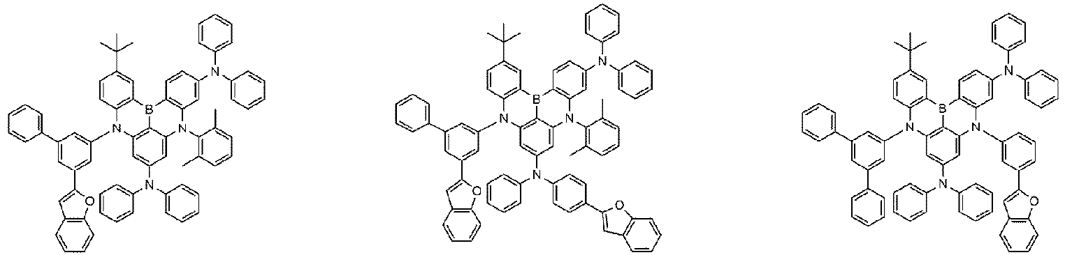
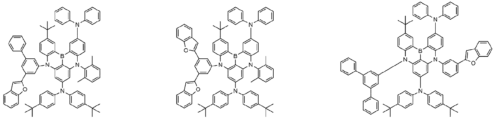
- the present disclosure provides the compound represented by Chemical Formula 1.
- the compound represented by Chemical Formula 1 contains at least one benzofuranyl or benzothiophenyl in its molecular structure.
- the compound represented by Chemical Formula 1 not only is easy to synthesize, but also contains at least one benzofuranyl or benzothiophenyl in the molecular structure, whereby it is advantageous for increasing the solubility in a solvent and manufacturing an organic light emitting device by a solution process such as an inkjet process.
- the compound represented by Chemical Formula 1 contains one, two, three or four benzofuranyl or benzothiophenyl in the molecular structure.
- the benzofuranyl is benzofuran-2-yl and the benzothiophenyl is benzothiophen-2-yl
- Ar 1 to Ar 4 are each independently a substituted or unsubstituted C 6-20 aromatic ring; or a C 2-20 heteroaromatic ring containing at least one heteroatom selected from the group consisting of N, O and S.
- Ar 1 to Ar 4 are each independently benzene, naphthalene, dibenzofuran, or dibenzothiophene.
- Ar 1 is benzene
- Ar 2 to Ar 4 are each independently benzene, naphthalene, dibenzofuran, or dibenzothiophene.
- R 1 is benzofuranyl or benzothiophenyl; and the rest are each independently hydrogen, deuterium, halogen, a C 1-10 alkyl, a substituted or unsubstituted C 6-20 aryl; or N (substituted or unsubstituted C 6-60 aryl) 2 ; or two adjacent R 1 s are connected to each other to form
- R 1 is benzofuranyl or benzothiophenyl; and the rest are each independently hydrogen, deuterium, methyl, ethyl, propyl, isopropyl, butyl, isobutyl, tertbutyl, or phenyl; or two adjacent R 1 s are connected to each other to form
- Chemical Formula 1 is represented by the following Chemical Formulas 1-1, 1-2, or 1-3: wherein in Chemical Formula 1-1 to 1-3, Ar 1 to Ar 4 and R 1 are as defined above.
- Step 1 is an amine substitution reaction, which is preferably carried out in the presence of a palladium catalyst and a base, and a reactive group for the amine substitution reaction can be modified as known in the art.
- Step 2 is a reaction with BI 3 , which is preferably carried out in the presence of a base.
- the above preparation method may be further embodied in Preparation Examples described hereinafter.
- the compound according to the present disclosure can form an organic material layer, particularly a light emitting layer, of an organic light emitting device by a solution process.
- the present disclosure provides a coating composition including the above-mentioned compound according to the present disclosure and a solvent.
- the solvent is not particularly limited as long as it is a solvent capable of dissolving or dispersing the compound according to the present disclosure.
- the solvent may include chlorine-based solvents such as chloroform, methylene chloride, 1,2-dichloroethane, 1,1,2-trichloroethane, chlorobenzene and o-dichlorobenzene; ether-based solvents such as tetrahydrofuran and dioxane; aromatic hydrocarbon-based solvents such as toluene, xylene, trimethylbenzene, and mesitylene; aliphatic hydrocarbon-based solvents such as cyclohexane, methylcyclohexane, n-pentane, n-hexane, n-heptane, n-octane, n-nonane and n-decane; ketone-based solvents such as acetone, methyl ethyl ketone, and cyclohex
- the coating composition may further include a compound used as a host material, and the compound used for the host material will be described later. Further, the coating composition may include a compound used as a dopant material, and the compound used for the dopant material will be described later.
- the viscosity of the coating composition is preferably 1 cP to 10 cP, and coating is easily carried out in the above range.
- the concentration of the compound according to the present disclosure in the coating composition is preferably 0.1 wt/v% to 20 wt/v%.
- the method includes the steps of: coating the above-mentioned light emitting layer according to the present disclosure onto the anode by a solution process; and heat-treating the coated coating composition.
- the solution process uses the above-mentioned coating composition according to the present disclosure, and refers to spin coating, dip coating, doctor blading, inkjet printing, screen printing, spray method, roll coating, and the like, but is not limited thereto.
- the heat treatment temperature in the heat treatment step is preferably from 150 to 230°C. Further, a heat treatment time may be 1 minute to 3 hours, more preferably 10 minutes to 1 hour. Further, the heat treatment is preferably carried out in an inert gas atmosphere such as argon and nitrogen.
- an organic light emitting device including the compound represented by Chemical Formula 1.
- the present disclosure provides an organic light emitting device comprising: a first electrode; a second electrode that is provided opposite to the first electrode; and one or more organic material layers that are provided between the first electrode and the second electrode, wherein one or more layers of the organic material layers include the compound represented by Chemical Formula 1.
- the organic material layer of the organic light emitting device of the present disclosure may have a single-layer structure, or it may have a multilayered structure in which two or more organic material layers are stacked.
- the organic light emitting device of the present disclosure may have a structure comprising a hole injection layer, a hole transport layer, a light emitting layer, an electron transport layer, an electron injection layer and the like as the organic material layer.
- the structure of the organic light emitting device is not limited thereto, and it may include a smaller number of organic layers.
- the organic material layer may include a light emitting layer, wherein the light emitting layer may include the compound represented by Chemical Formula 1.
- the compound according to the present disclosure can be used as a dopant of the light emitting layer.
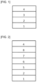
- the organic light emitting device according to the present disclosure may be a normal type organic light emitting device in which an anode, one or more organic material layers and a cathode are sequentially stacked on a substrate. Further, the organic light emitting device according to the present disclosure may be an inverted type organic light emitting device in which a cathode, one or more organic material layers and an anode are sequentially stacked on a substrate. For example, the structure of an organic light emitting device according to an embodiment of the present disclosure is illustrated in FIGS. 1 and 2 .
- FIG. 1 shows an example of an organic light emitting device comprising a substrate 1, an anode 2, a light emitting layer 3, and a cathode 4.
- the compound represented by Chemical Formula 1 may be included in the light emitting layer.
- FIG. 2 shows an example of an organic light emitting device comprising a substrate 1, an anode 2, a hole injection layer 5, a hole transport layer 6, a light emitting layer 7, an electron injection and transport layer 8, and a cathode 4.
- the compound represented by Chemical Formula 1 may be included in the light emitting layer.
- the organic light emitting device according to the present disclosure may be manufactured by materials and methods known in the art, except that at least one of the organic material layers includes the compound represented by Chemical Formula 1. Further, when the organic light emitting device includes a plurality of organic material layers, the organic material layers may be formed of the same material or different materials.
- the organic light emitting device can be manufactured by sequentially stacking an anode, an organic material layer and a cathode on a substrate.
- the organic light emitting device may be manufactured by depositing a metal, metal oxides having conductivity, or an alloy thereof on the substrate using a PVD (physical vapor deposition) method such as a sputtering method or an e-beam evaporation method to form an anode, forming organic material layers including the hole injection layer, the hole transport layer, the light emitting layer and the electron transport layer thereon, and then depositing a material that can be used as the cathode thereon.
- PVD physical vapor deposition
- the organic light emitting device may be manufactured by sequentially depositing a cathode material, an organic material layer and an anode material on a substrate (International Publication WO 2003/012890 ).
- the manufacturing method is not limited thereto.
- the first electrode is an anode
- the second electrode is a cathode
- the first electrode is a cathode and the second electrode is an anode
- anode material generally, a material having a large work function is preferably used so that holes can be smoothly injected into the organic material layer.
- the anode material include metals such as vanadium, chrome, copper, zinc, and gold, or an alloy thereof; metal oxides such as zinc oxides, indium oxides, indium tin oxides (ITO), and indium zinc oxides (IZO); a combination of metals and oxides, such as ZnO:AI or SnO 2 :Sb; conductive compounds such as poly(3-methylthiophene), poly[3,4-(ethylene-1,2-dioxy)thiophene](PEDOT), polypyrrole, and polyaniline, and the like, but are not limited thereto.
- the cathode material generally, a material having a small work function is preferably used so that electrons can be easily injected into the organic material layer.
- the cathode material include metals such as magnesium, calcium, sodium, potassium, titanium, indium, yttrium, lithium, gadolinium, aluminum, silver, tin, and lead, or an alloy thereof; a multilayered structure material such as LiF/Al or LiO 2 /Al, and the like, but are not limited thereto.
- the hole injection layer is a layer for injecting holes from the electrode, and the hole injection material is preferably a compound which has a capability of transporting the holes, thus has a hole injecting effect in the anode and an excellent hole injecting effect to the light emitting layer or the light emitting material, prevents excitons produced in the light emitting layer from moving to a hole injection layer or the electron injection material, and further is excellent in the ability to form a thin film. It is preferable that a HOMO (highest occupied molecular orbital) of the hole injection material is between the work function of the anode material and a HOMO of a peripheral organic material layer.
- a HOMO highest occupied molecular orbital
- the hole injection material examples include metal porphyrine, oligothiophene, an arylamine-based organic material, a hexanitrilehexaazatriphenylene-based organic material, a quinacridone-based organic material, a perylene-based organic material, anthraquinone, polyaniline and polythiophene-based conductive polymer, and the like, but are not limited thereto.
- the hole transport layer is a layer that receives holes from a hole injection layer and transports the holes to the light emitting layer.
- the hole transport material is suitably a material having large mobility to the holes, which may receive holes from the anode or the hole injection layer and transfer the holes to the light emitting layer.
- Specific examples thereof include an arylamine-based organic material, a conductive compound, a block copolymer in which a conjugate portion and a non-conjugate portion are present together, and the like, but are not limited thereto.
- the light emitting layer may include a host material and a dopant material.
- the host material may be a fused aromatic ring derivative, a heterocycle-containing compound or the like.
- the fused aromatic ring derivatives include anthracene derivatives, pyrene derivatives, naphthalene derivatives, pentacene derivatives, phenanthrene compounds, fluoranthene compounds, and the like.
- the heterocyclic-containing compounds include carbazole derivatives, dibenzofuran derivatives, ladder-type furan compounds, pyrimidine derivatives, and the like, but are not limited thereto.
- the dopant material examples include an aromatic amine derivative, a styrylamine compound, a boron complex, a fluoranthene compound, a metal complex, and the like.
- the aromatic amine derivative is a substituted or unsubstituted fused aromatic ring derivative having an arylamino group, and examples thereof include pyrene, anthracene, chrysene, periflanthene and the like, which have an arylamino group.
- the styrylamine compound is a compound where at least one arylvinyl group is substituted in substituted or unsubstituted arylamine, in which one or two or more substituent groups selected from the group consisting of an aryl group, a silyl group, an alkyl group, a cycloalkyl group, and an arylamino group are substituted or unsubstituted.
- substituent groups selected from the group consisting of an aryl group, a silyl group, an alkyl group, a cycloalkyl group, and an arylamino group are substituted or unsubstituted.
- Specific examples thereof include styrylamine, styryldiamine, styryltriamine, styryltetramine, and the like, but are not limited thereto.
- the metal complex includes an iridium complex, a platinum complex, and the like, but is not limited thereto.
- the electron injection and transport layer is a layer for simultaneously performing the roles of an electron transport layer and an electron injection layer that inject electrons from an electrode and transport the received electrons up to the light emitting layer, and is formed on the light emitting layer or the electron adjustment layer.
- the electron injection and transport material is suitably a material which can receive electrons well from a cathode and transfer the electrons to a light emitting layer, and has a large mobility for electrons.
- Specific examples of the electron injection and transport material include: an Al complex of 8-hydroxyquinoline; a complex including Alq 3 ; an organic radical compound; a hydroxyflavone-metal complex, a triazine derivative, and the like, but are not limited thereto.
- LiF, NaF, NaCl, CsF, Li 2 O, BaO, fluorenone, anthraquinodimethane, diphenoquinone, thiopyran dioxide, oxazole, oxadiazole, triazole, imidazole, perylenetetracarboxylic acid, fluorenylidene methane, anthrone, and the like, and derivatives thereof, a metal complex compound, a nitrogen-containing 5-membered ring derivative, and the like can be used, but are not limited thereto.
- Examples of the metal complex compound include 8-hydroxyquinolinato lithium, bis(8-hydroxyquinolinato)zinc, bis(8-hydroxyquinolinato)copper, bis(8-hydroxyquinolinato)manganese, tris(8-hydroxyquinolinato)aluminum, tris(2-methyl-8-hydroxyquinolinato)aluminum, tris(8-hydroxyquinolinato)gallium, bis(10-hydroxybenzo[h]quinolinato)beryllium, bis(10-hydroxybenzo[h]quinolinato)zinc, bis(2-methyl-8-quinolinato)chlorogallium, bis(2-methyl-8-quinolinato)(o-cresolato)gallium, bis(2-methyl-8-quinolinato)(1-naphtholato)aluminum, bis(2-methyl-8-quinolinato)(2-naphtholato)gallium, and the like, but are not limited thereto.
- the organic light emitting device may be a frontside emission type, a backside emission type, or a double-sided emission type based on the used material.
- the compound according to the present disclosure may be included in an organic solar cell or an organic transistor in addition to an organic light emitting device.
- Compound 1-i (yield: 62%) was prepared in the same manner as in the preparation method of Compound 1-e, except that Compound 1-g was used instead of Compound 1-d and Compound 1-h was used instead of Compound 1-c.
- Compound 2-a (yield: 67%) was prepared in the same manner as in the preparation method of Compound 1-k, except that Compound 1-I was used instead of Compound 1-i and Compound 1-k was used instead of Compound 1-j.
- Compound 2-b (yield: 56%) was prepared in the same manner as in the preparation method of Compound 1-e, except that Compound 2-a was used instead of Compound 1-d and Compound 1-e was used instead of Compound 1-c.
- Compound 3-b (yield: 50%) was prepared in the same manner as in the preparation method of Compound 1-k, except that Compound 3-a was used instead of Compound 1-i and Compound 1-k was used instead of Compound 1-j.
- Compound 4-c (yield: 81%) was prepared in the same manner as in the preparation method of Compound 1-e, except that Compound 4-a was used instead of Compound 1-d and Compound 4-b was used instead of Compound 1-c.
- Compound 4-d (yield: 70%) was prepared in the same manner as in the preparation method of Compound 1-k, except that Compound 4-c was used instead of Compound 1-i.
- Compound 4-f (yield: 64%) was prepared in the same manner as in the preparation method of Compound 1-e, except that Compound 4-e was used instead of Compound 1-d and Compound 1-e was used instead of Compound 1-c.
- Compound 5-c (yield: 73%) was prepared in the same manner as in the preparation method of Compound 1-k, except that Compound 5-b was used instead of Compound 1-i and Compound 4-d was used instead of Compound 1-j.
- Compound 5-d (yield: 64%) was prepared in the same manner as in the preparation method of Compound 1-e, except that Compound 5-c was used instead of Compound 1-d and Compound 1-I was used instead of Compound 1-c.
- Compound 6-a (yield: 79%) was prepared in the same manner as in the preparation method of Compound 1, except that Compound 5-c was used instead of Compound 1-d and Compound 1-1 was used instead of Compound 1-c.
- Compound 7-a (yield: 60%) was prepared in the same manner as in the preparation method of Compound 1-k, except that Compound 5-b was used instead of Compound 1-i and Compound 1-k was used instead of Compound 1-j.
- Compound 7-b (yield: 76%) was prepared in the same manner as in the preparation method of Compound 1-e, except that Compound 7-a was used instead of Compound 1-d and Compound 1-e was used instead of Compound 1-c.
- Compound 8-e was prepared in the same manner as in the preparation method of Compound 1-i, except that Compound 8-a was used instead of Compound 1-b.
- Compound 8-g (yield: 49%) was prepared in the same manner as in the preparation method of Compound 1-e, except that Compound 8-f was used instead of Compound 1-d and Compound 3-a was used instead of Compound 1-c.
- Compound 9-c (yield: 52%) was prepared in the same manner as in the preparation method of Compound 1-e, except that Compound 9-b was used instead of Compound 1-d and Compound 1-e was used instead of Compound 1-c.
- a glass substrate on which ITO (indium tin oxide) was coated as a thin film to a thickness of 500 ⁇ was put into distilled water in which a detergent was dissolved, and ultrasonically cleaned.
- a product manufactured by Fischer Co. was used as the detergent, and as the distilled water, distilled water filtered twice using a filter manufactured by Millipore Co. was used.
- ultrasonic cleaning was repeated twice using distilled water for 10 minutes.
- the substrate was ultrasonically cleaned with solvents of isopropyl alcohol, acetone, and methanol, dried, and then the substrate was cleaned for 5 minutes and then transferred to a glove box.
- a coating composition in which the following compound O and compound P (weight ratio of 2:8) were dissolved in cyclohexanone at 20 wt/v%, was spin-coated (4000 rpm) on the ITO transparent electrode, and heat-treated (cured) at 200°C for 30 minutes to form a hole injection layer with a thickness of 400 ⁇ .
- a coating composition in which the following polymer Q (Mn: 27,900; Mw: 35,600; measured by GPC (Agilent 1200 series) using PC Standard) was dissolved in toluene at 6 wt/v%, was spin-coated (4000 rpm) on the hole injection layer, and heat-treated at 200°C for 30 minutes to form a hole transport layer with a thickness of 200 ⁇ .
- a coating composition in which the previously prepared compound 1 and the following compound R (weight ratio of 2:98) were dissolved in cyclohexanone at 2 wt/v%, was spin-coated (4000 rpm) on the hole transport layer, and heat-treated at 180°C for 30 minutes to form a light emitting layer with a thickness of 400 ⁇ .
- the following compounds S was vacuum-deposited to a thickness of 350 ⁇ on the light emitting layer to form an electron injection and transport layer.
- LiF (10 ⁇ ), and aluminum (1000 ⁇ ) were sequentially deposited on the electron injection and transport layer to form a cathode.
- the vapor deposition rate of the organic material was maintained at 0.4 to 0.7 ⁇ /sec
- the deposition rate of LiF was maintained at 0.3 ⁇ /sec
- the deposition rate of aluminum was maintained at 2 ⁇ /sec
- the degree of vacuum during the deposition was maintained at 2 ⁇ 10 -7 to 5 ⁇ 10 -8 torr (2.7 ⁇ 10 -5 Pa to 6.7 ⁇ 10 -6 Pa).
- An organic light emitting device was manufactured in the same manner as in Experimental Example 1, except that the compounds shown in Table 1 below were used instead of Compound 1 as the dopant of the light emitting layer.
- the driving voltage, external quantum efficiency (EQE), and lifetime were measured by applying a current of 10 mA/cm 2 to the organic light emitting devices manufactured in the Experimental Examples and Comparative Experimental Examples, and the results are shown in Table 1 below.
- the external quantum efficiency (EQE) was calculated as "(the number of emitted photon)/(the number of injected charge carrier) ⁇ 100", and T90 means the time required for the luminance to be reduced to 90% of the initial luminance (500 nit).
- T90 means the time required for the luminance to be reduced to 90% of the initial luminance (500 nit).
- the organic light emitting devices comprising the compounds of the present disclosure as the dopant of the light emitting layer exhibits excellent characteristics in terms of efficiency, driving voltage and lifetime.
- substrate 2 anode 3: light emitting layer 4: cathode 5: hole injection layer 6: hole transport layer 7: light emitting layer 8: electron injection and transport layer
Landscapes
- Chemical & Material Sciences (AREA)
- Physics & Mathematics (AREA)
- Engineering & Computer Science (AREA)
- Materials Engineering (AREA)
- Spectroscopy & Molecular Physics (AREA)
- Organic Chemistry (AREA)
- Optics & Photonics (AREA)
- Electroluminescent Light Sources (AREA)
- Inorganic Chemistry (AREA)
Claims (10)
- Verbindung, dargestellt durch die folgende chemische Formel 1:
 Ar1 bis Ar4 jeweils unabhängig ein substituierter oder unsubstituierter aromatischer C6-60-Ring oder ein heteroaromatischer C2-60-Ring sind, der mindestens ein Heteroatom, ausgewählt aus der Gruppe, bestehend aus N, O und S, enthält,mindestens eines von R1 Benzofuranyl oder Benzothiophenyl ist und der Rest jeweils unabhängig Wasserstoff, Deuterium, Halogen, Cyano, ein substituiertes oder unsubstituiertes C1-60-Alkyl, ein substituiertes oder unsubstituiertes C2-60-Alkenyl, ein substituiertes oder unsubstituiertes C2-60-Alkinyl, ein substituiertes oder unsubstituiertes C3-30-Cycloalkyl, ein substituiertes oder unsubstituiertes C6-60-Aryl oder N (substituiertes oder unsubstituiertes C6-60-Aryl)2 ist oder zwei benachbarte R1 miteinander verbunden sind, um ein substituiertes oder unsubstituiertes C3-6-Alkylen zu bilden.
 - Verbindung nach Anspruch 1, wobei
Ar1 bis Ar4 jeweils unabhängig ein substituierter oder unsubstituierter aromatischer C6-20-Ring oder ein heteroaromatischer C2-20-Ring sind, der mindestens ein Heteroatom, ausgewählt aus der Gruppe, bestehend aus N, O und S, enthält. - Verbindung nach Anspruch 1, wobei
Ar1 bis Ar4 jeweils unabhängig Benzol, Naphthalin, Dibenzofuran oder Dibenzothiophen sind. - Verbindung nach Anspruch 1, wobei
Ar1 Benzol ist und Ar2 bis Ar4 jeweils unabhängig Benzol, Naphthalin, Dibenzofuran oder Dibenzothiophen sind. - Verbindung nach Anspruch 1, wobei
mindestens eines von R1 Benzofuranyl oder Benzothiophenyl ist und der Rest jeweils unabhängig Wasserstoff, Deuterium, Halogen, ein C1-10-Alkyl, ein substituiertes oder unsubstituiertes C6-20-Aryl oder N (substituiertes oder unsubstituiertes C6-60-Aryl)2 ist oder zwei benachbarte R1 miteinander verbunden sind, um
- Verbindung nach Anspruch 1, wobei
mindestens eines von R1 Benzofuranyl oder Benzothiophenyl ist und der Rest jeweils unabhängig Wasserstoff, Deuterium, Methyl, Ethyl, Propyl, Isopropyl, Butyl, Isobutyl, Tertbutyl oder Phenyl ist oder zwei benachbarte R1 miteinander verbunden sind, um
- Verbindung nach Anspruch 1, wobei
die chemische Formel 1 durch die folgende chemische Formel 1-1, 1-2 oder 1-3 dargestellt ist:


Ar1 bis Ar4 und R1 so wie in Anspruch 1 definiert sind. - Verbindung nach Anspruch 1, wobei
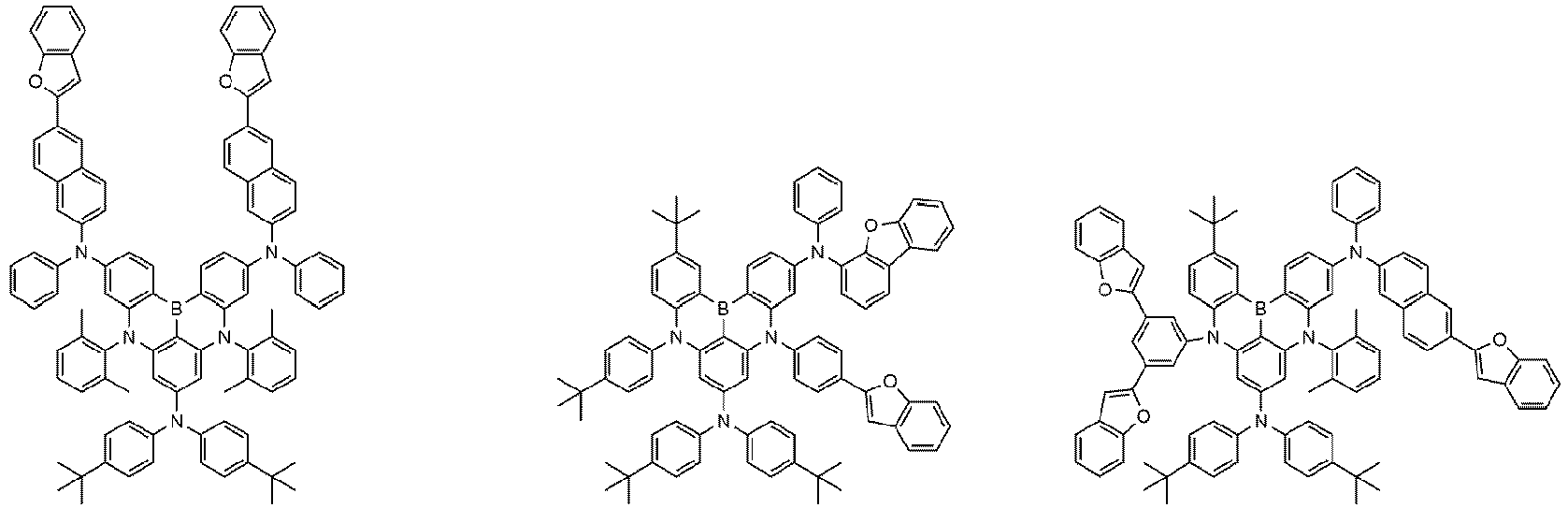
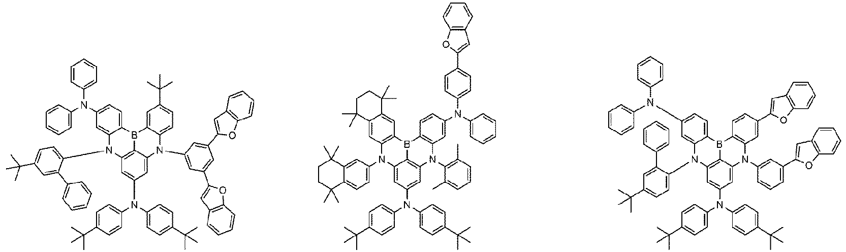
die durch die chemische Formel 1 dargestellte Verbindung eine, ausgewählt aus der Gruppe, bestehend aus den Folgenden, ist: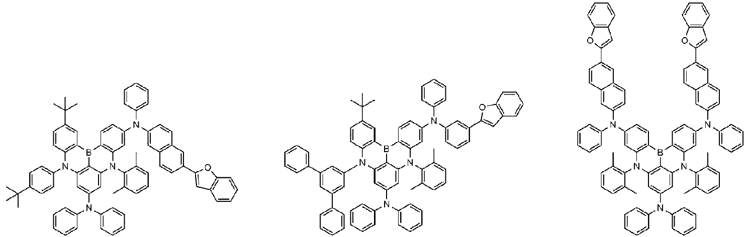


- Organische lichtemittierende Vorrichtung, umfassend: eine erste Elektrode, eine zweite Elektrode, die sich gegenüber der ersten Elektrode befindet, und eine oder mehr Schichten aus organischem Material, die sich zwischen der ersten Elektrode und der zweiten Elektrode befinden, wobei eine oder mehr Schichten der Schichten aus organischem Material die Verbindung gemäß einem der Ansprüche 1 bis 8 umfasst.
- Organische lichtemittierende Vorrichtung nach Anspruch 9, wobei
die Schicht aus organischem Material, die die Verbindung umfasst, eine lichtemittierende Schicht ist.
Applications Claiming Priority (2)
| Application Number | Priority Date | Filing Date | Title |
|---|---|---|---|
| KR1020210000317A KR102819367B1 (ko) | 2021-01-04 | 2021-01-04 | 신규한 화합물 및 이를 이용한 유기 발광 소자 |
| PCT/KR2021/018274 WO2022145775A1 (ko) | 2021-01-04 | 2021-12-03 | 신규한 화합물 및 이를 이용한 유기 발광 소자 |
Publications (3)
| Publication Number | Publication Date |
|---|---|
| EP4227312A1 EP4227312A1 (de) | 2023-08-16 |
| EP4227312A4 EP4227312A4 (de) | 2024-05-15 |
| EP4227312B1 true EP4227312B1 (de) | 2025-01-29 |
Family
ID=82260536
Family Applications (1)
| Application Number | Title | Priority Date | Filing Date |
|---|---|---|---|
| EP21915573.6A Active EP4227312B1 (de) | 2021-01-04 | 2021-12-03 | Neuartige verbindung und organische lichtemittierende vorrichtung damit |
Country Status (6)
| Country | Link |
|---|---|
| US (1) | US20230406867A1 (de) |
| EP (1) | EP4227312B1 (de) |
| JP (1) | JP7562218B2 (de) |
| KR (1) | KR102819367B1 (de) |
| CN (1) | CN116472796A (de) |
| WO (1) | WO2022145775A1 (de) |
Families Citing this family (5)
| Publication number | Priority date | Publication date | Assignee | Title |
|---|---|---|---|---|
| US20200111962A1 (en) * | 2018-10-03 | 2020-04-09 | Idemitsu Kosan Co., Ltd. | Organic electroluminescence device and electronic apparatus provided with the same |
| EP4379018A1 (de) | 2022-12-02 | 2024-06-05 | Idemitsu Kosan Co., Ltd | Verbindung und organische elektrolumineszenzvorrichtung mit der verbindung |
| EP4431516A1 (de) | 2023-03-15 | 2024-09-18 | Idemitsu Kosan Co., Ltd | Verbindung und organische elektrolumineszenzvorrichtung mit der verbindung |
| CN121100164A (zh) * | 2023-12-06 | 2025-12-09 | 出光兴产株式会社 | 化合物和包含该化合物的有机电致发光器件 |
| EP4567088A1 (de) * | 2023-12-06 | 2025-06-11 | Idemitsu Kosan Co.,Ltd. | Verbindung und organische elektrolumineszenzvorrichtung mit der verbindung |
Family Cites Families (8)
| Publication number | Priority date | Publication date | Assignee | Title |
|---|---|---|---|---|
| KR100430549B1 (ko) | 1999-01-27 | 2004-05-10 | 주식회사 엘지화학 | 신규한 착물 및 그의 제조 방법과 이를 이용한 유기 발광 소자 및 그의 제조 방법 |
| DE10135513B4 (de) | 2001-07-20 | 2005-02-24 | Novaled Gmbh | Lichtemittierendes Bauelement mit organischen Schichten |
| TWI636056B (zh) | 2014-02-18 | 2018-09-21 | 學校法人關西學院 | 多環芳香族化合物及其製造方法、有機元件用材料及其應用 |
| KR20190138477A (ko) * | 2018-06-05 | 2019-12-13 | 에스에프씨 주식회사 | 저전압구동이 가능하며 고효율의 유기 발광 소자 |
| KR102216430B1 (ko) * | 2018-07-19 | 2021-02-17 | 주식회사 엘지화학 | 다환 화합물 및 이를 포함하는 유기 발광 소자 |
| KR102725258B1 (ko) * | 2018-12-18 | 2024-11-04 | 삼성디스플레이 주식회사 | 붕소 및 질소를 포함하는 헤테로고리 화합물을 포함하는 유기 발광 소자 |
| WO2020200884A1 (en) | 2019-03-29 | 2020-10-08 | Cynora Gmbh | Organic molecules for optoelectronic devices |
| CN114026147A (zh) | 2019-06-14 | 2022-02-08 | 学校法人关西学院 | 多环芳香族化合物 |
-
2021
- 2021-01-04 KR KR1020210000317A patent/KR102819367B1/ko active Active
- 2021-12-03 CN CN202180076584.9A patent/CN116472796A/zh active Pending
- 2021-12-03 EP EP21915573.6A patent/EP4227312B1/de active Active
- 2021-12-03 US US18/036,991 patent/US20230406867A1/en active Pending
- 2021-12-03 WO PCT/KR2021/018274 patent/WO2022145775A1/ko not_active Ceased
- 2021-12-03 JP JP2023527101A patent/JP7562218B2/ja active Active
Also Published As
| Publication number | Publication date |
|---|---|
| CN116472796A (zh) | 2023-07-21 |
| KR102819367B1 (ko) | 2025-06-10 |
| EP4227312A4 (de) | 2024-05-15 |
| EP4227312A1 (de) | 2023-08-16 |
| KR20220098520A (ko) | 2022-07-12 |
| WO2022145775A1 (ko) | 2022-07-07 |
| JP2023547680A (ja) | 2023-11-13 |
| US20230406867A1 (en) | 2023-12-21 |
| JP7562218B2 (ja) | 2024-10-07 |
Similar Documents
| Publication | Publication Date | Title |
|---|---|---|
| EP4230629B1 (de) | Neuartige verbindung und organische lichtemittierende vorrichtung damit | |
| EP4227312B1 (de) | Neuartige verbindung und organische lichtemittierende vorrichtung damit | |
| EP4273151A1 (de) | Neuartige verbindung und organische lichtemittierende vorrichtung damit | |
| EP4230630B1 (de) | Neuartige verbindung und diese enthaltende organische lichtemittierende vorrichtung | |
| KR102641909B1 (ko) | 신규한 화합물 및 이를 이용한 유기발광 소자 | |
| EP4242214B1 (de) | Neuartige verbindung und organische lichtemittierende vorrichtung damit | |
| EP4265625B1 (de) | Neuartige verbindung und organische lichtemittierende vorrichtung damit | |
| EP4293030A1 (de) | Neuartige verbindung und organische lichtemittierende vorrichtung damit | |
| KR102712783B1 (ko) | 신규한 화합물 및 이를 이용한 유기 발광 소자 | |
| KR102589892B1 (ko) | 신규한 화합물 및 이를 이용한 유기발광 소자 | |
| EP4245760B1 (de) | Neuartige verbindung und organische lichtemittierende vorrichtung damit | |
| EP4279492B1 (de) | Neuartige verbindung und organische lichtemittierende vorrichtung damit | |
| EP4332107B1 (de) | Borhaltige heteroaromatische verbindungen und organische lichtemittierende vorrichtung damit | |
| EP4279493A1 (de) | Neuartige verbindung und organische lichtemittierende vorrichtung damit | |
| EP4335854A1 (de) | Neuartige verbindung und organische lichtemittierende vorrichtung damit | |
| KR102731527B1 (ko) | 신규한 화합물 및 이를 이용한 유기 발광 소자 | |
| KR102886634B1 (ko) | 신규한 화합물 및 이를 이용한 유기 발광 소자 | |
| EP3778582B1 (de) | Neue verbindung, beschichtungszusammensetzung, die diese umfasst und organische leuchtdiode, die diese umfasst |
Legal Events
| Date | Code | Title | Description |
|---|---|---|---|
| STAA | Information on the status of an ep patent application or granted ep patent |
Free format text: STATUS: THE INTERNATIONAL PUBLICATION HAS BEEN MADE |
|
| PUAI | Public reference made under article 153(3) epc to a published international application that has entered the european phase |
Free format text: ORIGINAL CODE: 0009012 |
|
| STAA | Information on the status of an ep patent application or granted ep patent |
Free format text: STATUS: REQUEST FOR EXAMINATION WAS MADE |
|
| 17P | Request for examination filed |
Effective date: 20230512 |
|
| AK | Designated contracting states |
Kind code of ref document: A1 Designated state(s): AL AT BE BG CH CY CZ DE DK EE ES FI FR GB GR HR HU IE IS IT LI LT LU LV MC MK MT NL NO PL PT RO RS SE SI SK SM TR |
|
| DAV | Request for validation of the european patent (deleted) | ||
| DAX | Request for extension of the european patent (deleted) | ||
| A4 | Supplementary search report drawn up and despatched |
Effective date: 20240416 |
|
| RIC1 | Information provided on ipc code assigned before grant |
Ipc: H10K 50/11 20230101ALI20240410BHEP Ipc: H10K 85/60 20230101ALI20240410BHEP Ipc: H10K 85/30 20230101ALI20240410BHEP Ipc: C09K 11/06 20060101ALI20240410BHEP Ipc: C07F 5/02 20060101AFI20240410BHEP |
|
| GRAP | Despatch of communication of intention to grant a patent |
Free format text: ORIGINAL CODE: EPIDOSNIGR1 |
|
| STAA | Information on the status of an ep patent application or granted ep patent |
Free format text: STATUS: GRANT OF PATENT IS INTENDED |
|
| RIC1 | Information provided on ipc code assigned before grant |
Ipc: H10K 50/11 20230101ALI20240726BHEP Ipc: H10K 85/60 20230101ALI20240726BHEP Ipc: H10K 85/30 20230101ALI20240726BHEP Ipc: C09K 11/06 20060101ALI20240726BHEP Ipc: C07F 5/02 20060101AFI20240726BHEP |
|
| INTG | Intention to grant announced |
Effective date: 20240826 |
|
| GRAS | Grant fee paid |
Free format text: ORIGINAL CODE: EPIDOSNIGR3 |
|
| GRAA | (expected) grant |
Free format text: ORIGINAL CODE: 0009210 |
|
| STAA | Information on the status of an ep patent application or granted ep patent |
Free format text: STATUS: THE PATENT HAS BEEN GRANTED |
|
| AK | Designated contracting states |
Kind code of ref document: B1 Designated state(s): AL AT BE BG CH CY CZ DE DK EE ES FI FR GB GR HR HU IE IS IT LI LT LU LV MC MK MT NL NO PL PT RO RS SE SI SK SM TR |
|
| REG | Reference to a national code |
Ref country code: GB Ref legal event code: FG4D |
|
| REG | Reference to a national code |
Ref country code: CH Ref legal event code: EP |
|
| REG | Reference to a national code |
Ref country code: DE Ref legal event code: R096 Ref document number: 602021025713 Country of ref document: DE |
|
| REG | Reference to a national code |
Ref country code: IE Ref legal event code: FG4D |
|
| REG | Reference to a national code |
Ref country code: NL Ref legal event code: MP Effective date: 20250129 |
|
| PG25 | Lapsed in a contracting state [announced via postgrant information from national office to epo] |
Ref country code: NL Free format text: LAPSE BECAUSE OF FAILURE TO SUBMIT A TRANSLATION OF THE DESCRIPTION OR TO PAY THE FEE WITHIN THE PRESCRIBED TIME-LIMIT Effective date: 20250129 |
|
| PG25 | Lapsed in a contracting state [announced via postgrant information from national office to epo] |
Ref country code: RS Free format text: LAPSE BECAUSE OF FAILURE TO SUBMIT A TRANSLATION OF THE DESCRIPTION OR TO PAY THE FEE WITHIN THE PRESCRIBED TIME-LIMIT Effective date: 20250429 |
|
| PG25 | Lapsed in a contracting state [announced via postgrant information from national office to epo] |
Ref country code: FI Free format text: LAPSE BECAUSE OF FAILURE TO SUBMIT A TRANSLATION OF THE DESCRIPTION OR TO PAY THE FEE WITHIN THE PRESCRIBED TIME-LIMIT Effective date: 20250129 |
|
| PG25 | Lapsed in a contracting state [announced via postgrant information from national office to epo] |
Ref country code: PL Free format text: LAPSE BECAUSE OF FAILURE TO SUBMIT A TRANSLATION OF THE DESCRIPTION OR TO PAY THE FEE WITHIN THE PRESCRIBED TIME-LIMIT Effective date: 20250129 |
|
| PG25 | Lapsed in a contracting state [announced via postgrant information from national office to epo] |
Ref country code: ES Free format text: LAPSE BECAUSE OF FAILURE TO SUBMIT A TRANSLATION OF THE DESCRIPTION OR TO PAY THE FEE WITHIN THE PRESCRIBED TIME-LIMIT Effective date: 20250129 |
|
| REG | Reference to a national code |
Ref country code: LT Ref legal event code: MG9D |
|
| PG25 | Lapsed in a contracting state [announced via postgrant information from national office to epo] |
Ref country code: IS Free format text: LAPSE BECAUSE OF FAILURE TO SUBMIT A TRANSLATION OF THE DESCRIPTION OR TO PAY THE FEE WITHIN THE PRESCRIBED TIME-LIMIT Effective date: 20250529 Ref country code: NO Free format text: LAPSE BECAUSE OF FAILURE TO SUBMIT A TRANSLATION OF THE DESCRIPTION OR TO PAY THE FEE WITHIN THE PRESCRIBED TIME-LIMIT Effective date: 20250429 |
|
| REG | Reference to a national code |
Ref country code: AT Ref legal event code: MK05 Ref document number: 1763373 Country of ref document: AT Kind code of ref document: T Effective date: 20250129 |
|
| PG25 | Lapsed in a contracting state [announced via postgrant information from national office to epo] |
Ref country code: HR Free format text: LAPSE BECAUSE OF FAILURE TO SUBMIT A TRANSLATION OF THE DESCRIPTION OR TO PAY THE FEE WITHIN THE PRESCRIBED TIME-LIMIT Effective date: 20250129 |
|
| PG25 | Lapsed in a contracting state [announced via postgrant information from national office to epo] |
Ref country code: PT Free format text: LAPSE BECAUSE OF FAILURE TO SUBMIT A TRANSLATION OF THE DESCRIPTION OR TO PAY THE FEE WITHIN THE PRESCRIBED TIME-LIMIT Effective date: 20250529 Ref country code: LV Free format text: LAPSE BECAUSE OF FAILURE TO SUBMIT A TRANSLATION OF THE DESCRIPTION OR TO PAY THE FEE WITHIN THE PRESCRIBED TIME-LIMIT Effective date: 20250129 |
|
| PG25 | Lapsed in a contracting state [announced via postgrant information from national office to epo] |
Ref country code: GR Free format text: LAPSE BECAUSE OF FAILURE TO SUBMIT A TRANSLATION OF THE DESCRIPTION OR TO PAY THE FEE WITHIN THE PRESCRIBED TIME-LIMIT Effective date: 20250430 Ref country code: BG Free format text: LAPSE BECAUSE OF FAILURE TO SUBMIT A TRANSLATION OF THE DESCRIPTION OR TO PAY THE FEE WITHIN THE PRESCRIBED TIME-LIMIT Effective date: 20250129 |
|
| PG25 | Lapsed in a contracting state [announced via postgrant information from national office to epo] |
Ref country code: AT Free format text: LAPSE BECAUSE OF FAILURE TO SUBMIT A TRANSLATION OF THE DESCRIPTION OR TO PAY THE FEE WITHIN THE PRESCRIBED TIME-LIMIT Effective date: 20250129 |
|
| PG25 | Lapsed in a contracting state [announced via postgrant information from national office to epo] |
Ref country code: SE Free format text: LAPSE BECAUSE OF FAILURE TO SUBMIT A TRANSLATION OF THE DESCRIPTION OR TO PAY THE FEE WITHIN THE PRESCRIBED TIME-LIMIT Effective date: 20250129 |
|
| PG25 | Lapsed in a contracting state [announced via postgrant information from national office to epo] |
Ref country code: SM Free format text: LAPSE BECAUSE OF FAILURE TO SUBMIT A TRANSLATION OF THE DESCRIPTION OR TO PAY THE FEE WITHIN THE PRESCRIBED TIME-LIMIT Effective date: 20250129 |
|
| PG25 | Lapsed in a contracting state [announced via postgrant information from national office to epo] |
Ref country code: DK Free format text: LAPSE BECAUSE OF FAILURE TO SUBMIT A TRANSLATION OF THE DESCRIPTION OR TO PAY THE FEE WITHIN THE PRESCRIBED TIME-LIMIT Effective date: 20250129 |
|
| PG25 | Lapsed in a contracting state [announced via postgrant information from national office to epo] |
Ref country code: IT Free format text: LAPSE BECAUSE OF FAILURE TO SUBMIT A TRANSLATION OF THE DESCRIPTION OR TO PAY THE FEE WITHIN THE PRESCRIBED TIME-LIMIT Effective date: 20250129 |
|
| PG25 | Lapsed in a contracting state [announced via postgrant information from national office to epo] |
Ref country code: CZ Free format text: LAPSE BECAUSE OF FAILURE TO SUBMIT A TRANSLATION OF THE DESCRIPTION OR TO PAY THE FEE WITHIN THE PRESCRIBED TIME-LIMIT Effective date: 20250129 Ref country code: EE Free format text: LAPSE BECAUSE OF FAILURE TO SUBMIT A TRANSLATION OF THE DESCRIPTION OR TO PAY THE FEE WITHIN THE PRESCRIBED TIME-LIMIT Effective date: 20250129 |
|
| PG25 | Lapsed in a contracting state [announced via postgrant information from national office to epo] |
Ref country code: RO Free format text: LAPSE BECAUSE OF FAILURE TO SUBMIT A TRANSLATION OF THE DESCRIPTION OR TO PAY THE FEE WITHIN THE PRESCRIBED TIME-LIMIT Effective date: 20250129 |
|
| PG25 | Lapsed in a contracting state [announced via postgrant information from national office to epo] |
Ref country code: SK Free format text: LAPSE BECAUSE OF FAILURE TO SUBMIT A TRANSLATION OF THE DESCRIPTION OR TO PAY THE FEE WITHIN THE PRESCRIBED TIME-LIMIT Effective date: 20250129 |
|
| REG | Reference to a national code |
Ref country code: DE Ref legal event code: R097 Ref document number: 602021025713 Country of ref document: DE |
|
| PLBE | No opposition filed within time limit |
Free format text: ORIGINAL CODE: 0009261 |
|
| STAA | Information on the status of an ep patent application or granted ep patent |
Free format text: STATUS: NO OPPOSITION FILED WITHIN TIME LIMIT |
|
| 26N | No opposition filed |
Effective date: 20251030 |
|
| PGFP | Annual fee paid to national office [announced via postgrant information from national office to epo] |
Ref country code: DE Payment date: 20251120 Year of fee payment: 5 |
|
| PGFP | Annual fee paid to national office [announced via postgrant information from national office to epo] |
Ref country code: FR Payment date: 20251125 Year of fee payment: 5 |