EP3951845B1 - Inspection device and inspection method - Google Patents
Inspection device and inspection method Download PDFInfo
- Publication number
- EP3951845B1 EP3951845B1 EP20780030.1A EP20780030A EP3951845B1 EP 3951845 B1 EP3951845 B1 EP 3951845B1 EP 20780030 A EP20780030 A EP 20780030A EP 3951845 B1 EP3951845 B1 EP 3951845B1
- Authority
- EP
- European Patent Office
- Prior art keywords
- light
- fluorescence
- wavelength
- quality
- emitting element
- Prior art date
- Legal status (The legal status is an assumption and is not a legal conclusion. Google has not performed a legal analysis and makes no representation as to the accuracy of the status listed.)
- Active
Links
Images


Classifications
-
- H—ELECTRICITY
- H01—ELECTRIC ELEMENTS
- H01L—SEMICONDUCTOR DEVICES NOT COVERED BY CLASS H10
- H01L22/00—Testing or measuring during manufacture or treatment; Reliability measurements, i.e. testing of parts without further processing to modify the parts as such; Structural arrangements therefor
- H01L22/10—Measuring as part of the manufacturing process
- H01L22/12—Measuring as part of the manufacturing process for structural parameters, e.g. thickness, line width, refractive index, temperature, warp, bond strength, defects, optical inspection, electrical measurement of structural dimensions, metallurgic measurement of diffusions
-
- G—PHYSICS
- G01—MEASURING; TESTING
- G01N—INVESTIGATING OR ANALYSING MATERIALS BY DETERMINING THEIR CHEMICAL OR PHYSICAL PROPERTIES
- G01N21/00—Investigating or analysing materials by the use of optical means, i.e. using sub-millimetre waves, infrared, visible or ultraviolet light
- G01N21/62—Systems in which the material investigated is excited whereby it emits light or causes a change in wavelength of the incident light
- G01N21/63—Systems in which the material investigated is excited whereby it emits light or causes a change in wavelength of the incident light optically excited
- G01N21/64—Fluorescence; Phosphorescence
- G01N21/6428—Measuring fluorescence of fluorescent products of reactions or of fluorochrome labelled reactive substances, e.g. measuring quenching effects, using measuring "optrodes"
-
- G—PHYSICS
- G01—MEASURING; TESTING
- G01N—INVESTIGATING OR ANALYSING MATERIALS BY DETERMINING THEIR CHEMICAL OR PHYSICAL PROPERTIES
- G01N21/00—Investigating or analysing materials by the use of optical means, i.e. using sub-millimetre waves, infrared, visible or ultraviolet light
- G01N21/62—Systems in which the material investigated is excited whereby it emits light or causes a change in wavelength of the incident light
- G01N21/63—Systems in which the material investigated is excited whereby it emits light or causes a change in wavelength of the incident light optically excited
- G01N21/64—Fluorescence; Phosphorescence
- G01N21/645—Specially adapted constructive features of fluorimeters
- G01N21/6456—Spatial resolved fluorescence measurements; Imaging
- G01N21/6458—Fluorescence microscopy
-
- G—PHYSICS
- G01—MEASURING; TESTING
- G01N—INVESTIGATING OR ANALYSING MATERIALS BY DETERMINING THEIR CHEMICAL OR PHYSICAL PROPERTIES
- G01N21/00—Investigating or analysing materials by the use of optical means, i.e. using sub-millimetre waves, infrared, visible or ultraviolet light
- G01N21/62—Systems in which the material investigated is excited whereby it emits light or causes a change in wavelength of the incident light
- G01N21/63—Systems in which the material investigated is excited whereby it emits light or causes a change in wavelength of the incident light optically excited
- G01N21/64—Fluorescence; Phosphorescence
- G01N21/6489—Photoluminescence of semiconductors
-
- G—PHYSICS
- G01—MEASURING; TESTING
- G01N—INVESTIGATING OR ANALYSING MATERIALS BY DETERMINING THEIR CHEMICAL OR PHYSICAL PROPERTIES
- G01N21/00—Investigating or analysing materials by the use of optical means, i.e. using sub-millimetre waves, infrared, visible or ultraviolet light
- G01N21/84—Systems specially adapted for particular applications
- G01N21/88—Investigating the presence of flaws or contamination
- G01N21/8806—Specially adapted optical and illumination features
-
- G—PHYSICS
- G01—MEASURING; TESTING
- G01N—INVESTIGATING OR ANALYSING MATERIALS BY DETERMINING THEIR CHEMICAL OR PHYSICAL PROPERTIES
- G01N21/00—Investigating or analysing materials by the use of optical means, i.e. using sub-millimetre waves, infrared, visible or ultraviolet light
- G01N21/84—Systems specially adapted for particular applications
- G01N21/88—Investigating the presence of flaws or contamination
- G01N21/8851—Scan or image signal processing specially adapted therefor, e.g. for scan signal adjustment, for detecting different kinds of defects, for compensating for structures, markings, edges
-
- G—PHYSICS
- G01—MEASURING; TESTING
- G01N—INVESTIGATING OR ANALYSING MATERIALS BY DETERMINING THEIR CHEMICAL OR PHYSICAL PROPERTIES
- G01N21/00—Investigating or analysing materials by the use of optical means, i.e. using sub-millimetre waves, infrared, visible or ultraviolet light
- G01N21/84—Systems specially adapted for particular applications
- G01N21/88—Investigating the presence of flaws or contamination
- G01N21/95—Investigating the presence of flaws or contamination characterised by the material or shape of the object to be examined
- G01N21/9501—Semiconductor wafers
- G01N21/9505—Wafer internal defects, e.g. microcracks
-
- G—PHYSICS
- G01—MEASURING; TESTING
- G01N—INVESTIGATING OR ANALYSING MATERIALS BY DETERMINING THEIR CHEMICAL OR PHYSICAL PROPERTIES
- G01N21/00—Investigating or analysing materials by the use of optical means, i.e. using sub-millimetre waves, infrared, visible or ultraviolet light
- G01N21/84—Systems specially adapted for particular applications
- G01N21/88—Investigating the presence of flaws or contamination
- G01N21/95—Investigating the presence of flaws or contamination characterised by the material or shape of the object to be examined
- G01N21/956—Inspecting patterns on the surface of objects
-
- G—PHYSICS
- G06—COMPUTING OR CALCULATING; COUNTING
- G06T—IMAGE DATA PROCESSING OR GENERATION, IN GENERAL
- G06T7/00—Image analysis
- G06T7/0002—Inspection of images, e.g. flaw detection
- G06T7/0004—Industrial image inspection
-
- H—ELECTRICITY
- H01—ELECTRIC ELEMENTS
- H01L—SEMICONDUCTOR DEVICES NOT COVERED BY CLASS H10
- H01L21/00—Processes or apparatus adapted for the manufacture or treatment of semiconductor or solid state devices or of parts thereof
- H01L21/67—Apparatus specially adapted for handling semiconductor or electric solid state devices during manufacture or treatment thereof; Apparatus specially adapted for handling wafers during manufacture or treatment of semiconductor or electric solid state devices or components ; Apparatus not specifically provided for elsewhere
- H01L21/67005—Apparatus not specifically provided for elsewhere
- H01L21/67242—Apparatus for monitoring, sorting or marking
- H01L21/67288—Monitoring of warpage, curvature, damage, defects or the like
-
- H—ELECTRICITY
- H10—SEMICONDUCTOR DEVICES; ELECTRIC SOLID-STATE DEVICES NOT OTHERWISE PROVIDED FOR
- H10H—INORGANIC LIGHT-EMITTING SEMICONDUCTOR DEVICES HAVING POTENTIAL BARRIERS
- H10H20/00—Individual inorganic light-emitting semiconductor devices having potential barriers, e.g. light-emitting diodes [LED]
- H10H20/80—Constructional details
- H10H20/81—Bodies
-
- G—PHYSICS
- G01—MEASURING; TESTING
- G01N—INVESTIGATING OR ANALYSING MATERIALS BY DETERMINING THEIR CHEMICAL OR PHYSICAL PROPERTIES
- G01N21/00—Investigating or analysing materials by the use of optical means, i.e. using sub-millimetre waves, infrared, visible or ultraviolet light
- G01N21/01—Arrangements or apparatus for facilitating the optical investigation
- G01N2021/0106—General arrangement of respective parts
- G01N2021/0112—Apparatus in one mechanical, optical or electronic block
-
- G—PHYSICS
- G01—MEASURING; TESTING
- G01N—INVESTIGATING OR ANALYSING MATERIALS BY DETERMINING THEIR CHEMICAL OR PHYSICAL PROPERTIES
- G01N21/00—Investigating or analysing materials by the use of optical means, i.e. using sub-millimetre waves, infrared, visible or ultraviolet light
- G01N21/62—Systems in which the material investigated is excited whereby it emits light or causes a change in wavelength of the incident light
- G01N21/63—Systems in which the material investigated is excited whereby it emits light or causes a change in wavelength of the incident light optically excited
- G01N21/64—Fluorescence; Phosphorescence
- G01N2021/6417—Spectrofluorimetric devices
- G01N2021/6421—Measuring at two or more wavelengths
-
- G—PHYSICS
- G01—MEASURING; TESTING
- G01N—INVESTIGATING OR ANALYSING MATERIALS BY DETERMINING THEIR CHEMICAL OR PHYSICAL PROPERTIES
- G01N21/00—Investigating or analysing materials by the use of optical means, i.e. using sub-millimetre waves, infrared, visible or ultraviolet light
- G01N21/62—Systems in which the material investigated is excited whereby it emits light or causes a change in wavelength of the incident light
- G01N21/63—Systems in which the material investigated is excited whereby it emits light or causes a change in wavelength of the incident light optically excited
- G01N21/64—Fluorescence; Phosphorescence
- G01N21/645—Specially adapted constructive features of fluorimeters
- G01N2021/6463—Optics
-
- G—PHYSICS
- G01—MEASURING; TESTING
- G01N—INVESTIGATING OR ANALYSING MATERIALS BY DETERMINING THEIR CHEMICAL OR PHYSICAL PROPERTIES
- G01N21/00—Investigating or analysing materials by the use of optical means, i.e. using sub-millimetre waves, infrared, visible or ultraviolet light
- G01N21/62—Systems in which the material investigated is excited whereby it emits light or causes a change in wavelength of the incident light
- G01N21/63—Systems in which the material investigated is excited whereby it emits light or causes a change in wavelength of the incident light optically excited
- G01N21/64—Fluorescence; Phosphorescence
- G01N21/645—Specially adapted constructive features of fluorimeters
- G01N2021/6484—Optical fibres
-
- G—PHYSICS
- G01—MEASURING; TESTING
- G01N—INVESTIGATING OR ANALYSING MATERIALS BY DETERMINING THEIR CHEMICAL OR PHYSICAL PROPERTIES
- G01N21/00—Investigating or analysing materials by the use of optical means, i.e. using sub-millimetre waves, infrared, visible or ultraviolet light
- G01N21/84—Systems specially adapted for particular applications
- G01N21/88—Investigating the presence of flaws or contamination
- G01N21/8806—Specially adapted optical and illumination features
- G01N2021/8845—Multiple wavelengths of illumination or detection
-
- G—PHYSICS
- G01—MEASURING; TESTING
- G01N—INVESTIGATING OR ANALYSING MATERIALS BY DETERMINING THEIR CHEMICAL OR PHYSICAL PROPERTIES
- G01N21/00—Investigating or analysing materials by the use of optical means, i.e. using sub-millimetre waves, infrared, visible or ultraviolet light
- G01N21/84—Systems specially adapted for particular applications
- G01N21/88—Investigating the presence of flaws or contamination
- G01N21/8851—Scan or image signal processing specially adapted therefor, e.g. for scan signal adjustment, for detecting different kinds of defects, for compensating for structures, markings, edges
- G01N2021/8854—Grading and classifying of flaws
- G01N2021/8858—Flaw counting
-
- G—PHYSICS
- G01—MEASURING; TESTING
- G01N—INVESTIGATING OR ANALYSING MATERIALS BY DETERMINING THEIR CHEMICAL OR PHYSICAL PROPERTIES
- G01N21/00—Investigating or analysing materials by the use of optical means, i.e. using sub-millimetre waves, infrared, visible or ultraviolet light
- G01N21/84—Systems specially adapted for particular applications
- G01N21/88—Investigating the presence of flaws or contamination
- G01N21/8851—Scan or image signal processing specially adapted therefor, e.g. for scan signal adjustment, for detecting different kinds of defects, for compensating for structures, markings, edges
- G01N2021/8854—Grading and classifying of flaws
- G01N2021/8861—Determining coordinates of flaws
-
- G—PHYSICS
- G01—MEASURING; TESTING
- G01N—INVESTIGATING OR ANALYSING MATERIALS BY DETERMINING THEIR CHEMICAL OR PHYSICAL PROPERTIES
- G01N21/00—Investigating or analysing materials by the use of optical means, i.e. using sub-millimetre waves, infrared, visible or ultraviolet light
- G01N21/84—Systems specially adapted for particular applications
- G01N21/88—Investigating the presence of flaws or contamination
- G01N21/8851—Scan or image signal processing specially adapted therefor, e.g. for scan signal adjustment, for detecting different kinds of defects, for compensating for structures, markings, edges
- G01N2021/8854—Grading and classifying of flaws
- G01N2021/888—Marking defects
-
- H—ELECTRICITY
- H10—SEMICONDUCTOR DEVICES; ELECTRIC SOLID-STATE DEVICES NOT OTHERWISE PROVIDED FOR
- H10H—INORGANIC LIGHT-EMITTING SEMICONDUCTOR DEVICES HAVING POTENTIAL BARRIERS
- H10H20/00—Individual inorganic light-emitting semiconductor devices having potential barriers, e.g. light-emitting diodes [LED]
- H10H20/01—Manufacture or treatment
Definitions
- An aspect of the present invention relates to an inspection apparatus and an inspection method.
- Patent Literature 2 relates to an inspection device of a fluorescent light emitting body, wherein the fluorescent light emitting body to be inspected is a LED chip which has a photoluminescence characteristic.
- the inspection device comprises an illumination unit configured to emit illumination light toward the LED chip and a fluorescence observation unit configured to observe light emitted from the fluorescent light emitter of the LED chip, wherein the fluorescence observation unit includes a first observation unit, a second observation unit, a first filter unit and a second filter unit.
- the first observation unit is configured to observe the light passing through the first filter unit and the second observation unit performs is configured to observe the light passing through the second filter unit.
- the first filter unit transmits light of a wavelength longer than the first wavelength and the second filter unit transmits light of a wavelength shorter than a second wavelength.
- the inspection method described in Patent Literature 1 focuses only on fluorescence of a normal emission spectrum.
- some light-emitting elements may have spots that emit light at longer wavelengths than the normal emission spectrum.
- the quality of the light-emitting element may not be determined in consideration of the fluorescence on the long wavelength side, and the quality of the light-emitting element may not be determined with high accuracy.
- An aspect of the invention has been made in view of the above circumstances, and an object of the invention is to determine the quality of a light-emitting element with high accuracy.
- An inspection apparatus is an inspection apparatus, as defined in claim 1, for inspecting an object on which a plurality of light-emitting elements is formed, the inspection apparatus including an excitation light source that generates excitation light to irradiate the object, a first imaging unit that images fluorescence having a wavelength longer than a first wavelength in fluorescence from the light-emitting elements, and a determining unit that determines a quality of each of the light-emitting elements based on a first fluorescence image acquired by the first imaging unit, in which the first wavelength is a wavelength obtained by adding a full width at half maximum of a normal fluorescence spectrum of the light-emitting element to a peak wavelength of the normal fluorescence spectrum.
- the quality of each of the light-emitting elements is determined based on a fluorescence image having a wavelength obtained by adding a full width at half maximum of a normal fluorescence spectrum of the light-emitting element to a peak wavelength of the normal fluorescence spectrum, that is, a fluorescence image on a long wavelength side that cannot be included in a normal fluorescence spectrum of the light-emitting element.
- Some light-emitting elements may have spots that emit light at longer wavelengths than the normal emission spectrum.
- the quality of the light-emitting element is determined based on such a fluorescence image on the long wavelength side, it is possible to appropriately detect the fluorescence spot on the long wavelength side, and to appropriately determine that a light-emitting element having the fluorescence spot is defective. That is, with the inspection apparatus according to the aspect of the invention, the quality of the light-emitting element can be determined with high accuracy by considering the fluorescence on the long wavelength side.
- the inspection apparatus includes, according to the claimed invention, an optical element that separates fluorescence from the light-emitting elements into fluorescence having a wavelength longer than the first wavelength and fluorescence having a wavelength shorter than a second wavelength, and a second imaging unit that images fluorescence having a wavelength shorter than the second wavelength, the fluorescence having a wavelength included in a normal fluorescence spectrum of the light-emitting element.
- an optical element that separates fluorescence from the light-emitting elements into fluorescence having a wavelength longer than the first wavelength and fluorescence having a wavelength shorter than a second wavelength
- a second imaging unit that images fluorescence having a wavelength shorter than the second wavelength, the fluorescence having a wavelength included in a normal fluorescence spectrum of the light-emitting element.
- the first wavelength and the second wavelength may be the same wavelength, and the optical element may be a dichroic mirror. According to such a configuration, it is possible to easily and reliably image the fluorescence on the long wavelength side and the fluorescence having the wavelength included in the normal fluorescence spectrum described above.
- the determining unit may determine a quality of each of the light-emitting elements based on the first fluorescence image and a second fluorescence image acquired by the second imaging unit. In this way, in addition to determining the quality of the light-emitting element in consideration of the fluorescence on the long wavelength side, it is possible to determine the quality of the light-emitting element based on the fluorescence having the wavelength included in the normal fluorescence spectrum. In this way, it is possible to determine the quality of the light-emitting element with higher accuracy in consideration of both the abnormality (fluorescence spot) on the long wavelength side and the light emission state in the normal fluorescence spectrum.
- the determining unit may determine a quality of each of the light-emitting elements based on the second fluorescence image, and determine a quality based on the first fluorescence image for a light-emitting element determined to be non-defective in the determination after the determination.
- a light-emitting element whose light emission state in the normal fluorescence spectrum is abnormal is appropriately determined to be defective, it is possible to further determine that a light-emitting element, which has an abnormality (fluorescence spot) on the long wavelength side even though a light emission state in the normal fluorescence spectrum is normal, is defective, and it is possible to identify a defective light-emitting element without omission in consideration of both the light emission state on the long wavelength side and the light emission state in the normal fluorescence spectrum.
- quality determination based on the first fluorescence image is performed only for a light-emitting element determined to be non-defective in quality determination based on the second fluorescence image, it is possible to shorten a time required for determination related to an abnormality on the long wavelength side.
- the determining unit may determine a quality of each of the light-emitting elements based on the second fluorescence image, and determine a quality based on the first fluorescence image for a light-emitting element determined to be defective in the determination after the determination.
- the light-emitting element may have no abnormality (fluorescence spot) on the long wavelength side, the light-emitting element can be determined to be non-defective, and it is possible to prevent a light-emitting element not having a serious abnormality (fluorescence spot on the long wavelength side) from being determined to be defective.
- the quality determination based on the first fluorescence image is performed only for a light-emitting element determined to be defective in the quality determination based on the second fluorescence image, it is possible to shorten a time required for determination related to an abnormality on the long wavelength side.
- the determining unit may determine a quality of each of the light-emitting elements based on a luminance of the second fluorescence image, and determine a quality of each of the light-emitting elements based on a bright spot contained in the first fluorescence image. According to such a configuration, the quality of the light-emitting element can be determined with higher accuracy in consideration of the luminance of the fluorescence in the normal fluorescence spectrum and information about the fluorescence spot on the long wavelength side (presence or absence and the number of abnormal fluorescence spots, etc.).
- the determining unit may output a quality determination result of each of the light-emitting elements. In this way, it is possible to identify a light-emitting element that affects the light emission efficiency and take measures to improve the light emission efficiency by using the quality determination result for each light-emitting element.
- the determining unit may identify a defective portion in the light-emitting elements, and output a position of the defective portion. For example, when a position of a fluorescence spot on the long wavelength side is identified based on an imaging result, and the position of the fluorescence spot is output as a defective portion, it is possible to take measures to improve the light emission efficiency based on information about the defective portion.
- An inspection method is an inspection method of inspecting an object on which a plurality of light-emitting elements is formed, the method including an excitation light irradiation step of irradiating the object with excitation light, a first imaging step of imaging fluorescence having a wavelength longer than a first wavelength in fluorescence from the light-emitting elements, and a determination step of determining a quality of each of the light-emitting elements based on a first fluorescence image acquired in the first imaging step, in which the first wavelength is a wavelength obtained by adding a full width at half maximum of a normal fluorescence spectrum of the light-emitting element to a peak wavelength of the normal fluorescence spectrum.
- the inspection method may further include a separation step of separating fluorescence from the light-emitting elements into fluorescence having a wavelength longer than the first wavelength and fluorescence having a wavelength shorter than a second wavelength, and a second imaging step of imaging fluorescence having a wavelength shorter than the second wavelength, the fluorescence having a wavelength included in a normal fluorescence spectrum of the light-emitting element.
- the first wavelength and the second wavelength may be the same wavelength.
- a quality of each of the light-emitting elements may be determined based on the first fluorescence image and a second fluorescence image acquired in the second imaging step.
- a quality of each of the light-emitting elements may be determined based on the second fluorescence image, and a quality may be determined based on the first fluorescence image for a light-emitting element determined to be non-defective in the determination after the determination.
- a quality of each of the light-emitting elements may be determined based on the second fluorescence image, and a quality may be determined based on the first fluorescence image for a light-emitting element determined to be defective in the determination after the determination.
- a quality of each of the light-emitting elements may be determined based on a luminance of the second fluorescence image, and a quality of each of the light-emitting elements may be determined based on a bright spot contained in the first fluorescence image.
- a quality determination result of each of the light-emitting elements may be output.
- a defective portion in the light-emitting elements may be identified, and a position of the defective portion may be output.
- the quality of the light-emitting element can be determined by acquiring a fluorescence image, so that the qualities of a large number of light-emitting elements can be efficiently determined without being bound by physical restrictions.
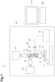
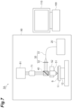
- the chuck 11 is a holding member that holds the sample S.
- the chuck 11 holds the sample S by, for example, vacuum-sucking the wafer of the sample S.
- the XY stage 12 is a stage for moving the chuck 11 holding the sample S in an XY direction (front-back and right-left directions), that is, in a direction along a mounting surface of the sample S on the chuck 11.
- the XY stage 12 moves the chuck 11 in the XY direction so that each of the plurality of light-emitting elements is sequentially set as an irradiation region of excitation light according to control of the control apparatus 100.
- the inspection apparatus 1 may further include a rotating stage ( ⁇ stage, not illustrated).
- Such a rotating stage may be provided, for example, above the XY stage 12 and below the chuck 11, or may be provided integrally with the XY stage 12.
- the rotating stage is used to accurately align vertical and horizontal positions of the sample S. By providing the rotating stage, it is possible to shorten a time for alignment, etc. and to shorten a total time for data processing.
- the excitation light source 20 is a light source that generates excitation light to irradiate the sample S and irradiates the sample S with excitation light.
- the excitation light source 20 may be a light source capable of generating light including a wavelength that excites the light-emitting element of the sample S, and is, for example, an LED, a laser, a halogen lamp, a mercury lamp, a D2 lamp, a plasma light source, etc.
- the inspection apparatus 1 may further include a sensor that monitors the illumination luminance to keep a luminance of excitation light emitted from the excitation light source 20 constant.
- the optical system 30 includes an optical fiber cable 31 and a light guide lens 32.
- the optical fiber cable 31 is an optical fiber cable for guiding light connected to the excitation light source 20.
- the light guide lens 32 is, for example, a single or composite convex lens, and guides excitation light arriving through the optical fiber cable 31 in a direction of the dichroic mirror 40.
- the inspection apparatus 1 may include a band-pass filter (not illustrated) between the excitation light source 20 and the dichroic mirror 40.
- the dichroic mirror 40 is a mirror made of a special optical material, and reflects light of a specific wavelength and transmits light of other wavelengths. Specifically, the dichroic mirror 40 is configured to reflect excitation light in a direction of the objective lens 51 and transmit photoluminescence (specifically, fluorescence) from the light-emitting element, which is light in a wavelength band different from that of excitation light, in a direction of the dichroic mirror 60. Note that, as shown in FIG. 2 , a region of a normal emission spectrum FS of excitation light is on a lower wavelength side of a region of a normal emission spectrum (normal fluorescence spectrum) ES of fluorescence.
- the dichroic mirror 40 reflects excitation light, which is light in a low wavelength band, in the direction of the objective lens 51, and transmits fluorescence, which is light in a higher wavelength band than that of excitation light, in the direction of the dichroic mirror 60.
- the objective lens 51 has a configuration for observing the sample S, and concentrates excitation light guided by the dichroic mirror 40 on the sample S.
- the Z stage 52 adjusts the focus by moving the objective lens 51 in a Z direction (vertical direction), that is, in a direction intersecting the mounting surface of the sample S on the chuck 11.
- the dichroic mirror 60 is a mirror made of a special optical material, and reflects light of a specific wavelength and transmits light of other wavelengths.
- the dichroic mirror 60 separates fluorescence from the light-emitting element into fluorescence having a wavelength longer than a first wavelength and fluorescence having a wavelength shorter than a second wavelength.
- the first wavelength and the second wavelength will be described as being the same wavelength (reference wavelength BW). That is, the dichroic mirror 60 separates fluorescence from the light-emitting element into fluorescence having a wavelength longer than the reference wavelength BW and fluorescence having a wavelength shorter than the reference wavelength BW.
- FIG. 2 is a diagram for description of an emission spectrum and characteristics of the dichroic mirrors 60 and 40.
- a horizontal axis represents a wavelength
- a left vertical axis represents emission luminance
- a right vertical axis represents transmittance.
- the above-mentioned reference wavelength BW is defined as a wavelength obtained by adding a full width at half maximum WH of a normal fluorescence spectrum ES of the light-emitting element to a peak wavelength PW of the normal fluorescence spectrum ES.
- fluorescence of a short wavelength reflected by the dichroic mirror 60 is fluorescence of a wavelength included in the normal fluorescence spectrum ES (fluorescence having an original emission wavelength)
- fluorescence of a long wavelength transmitted by the dichroic mirror 60 is fluorescence of a wavelength not included in the normal fluorescence spectrum ES (fluorescence on a long wavelength side).
- the original emission wavelength may be, for example, a wavelength known in advance from a specification of the light-emitting element, or may be a wavelength corresponding to a peak of intensity obtained by measuring fluorescence from the light-emitting element by a spectroscope.
- the dichroic mirror 60 transmits a part of fluorescence having a wavelength shorter than the reference wavelength BW and reflects a part of fluorescence having a wavelength longer than the reference wavelength BW (see FIG. 2 ).
- the dichroic mirror 60 reflects fluorescence having a wavelength shorter than the reference wavelength BW and transmits fluorescence having a wavelength longer than the reference wavelength BW.
- a description will be given simply on the assumption that "the dichroic mirror 60 reflects fluorescence having a wavelength shorter than the reference wavelength BW and transmits fluorescence having a wavelength longer than the reference wavelength BW".
- Fluorescence having a wavelength longer than the reference wavelength BW (fluorescence on the long wavelength side) reaches the imaging lens 71 via the dichroic mirror 60. Fluorescence having a wavelength shorter than the reference wavelength BW (fluorescence having the original emission wavelength) reaches the imaging lens 72 via the dichroic mirror 60.
- the imaging lens 71 is a lens that forms an image of fluorescence on the long wavelength side and guides the fluorescence to the camera 81.
- the camera 81 is an imaging unit that images fluorescence from the sample S. More specifically, the camera 81 images fluorescence having a wavelength longer than the reference wavelength BW (fluorescence on the long wavelength side) in fluorescence from the light-emitting element. The camera 81 images fluorescence on the long wavelength side by detecting the image formed by the imaging lens 71. The camera 81 outputs a fluorescence image on the long wavelength side, which is an imaging result, to the control apparatus 100.
- the camera 81 is, for example, an area image sensor such as a CCD or MOS. Further, the camera 81 may include a line sensor or a time delay integration (TDI) sensor. Note that the inspection apparatus 1 may further include a band-pass filter between the dichroic mirror 60 and the camera 81 to prevent unnecessary light emission on the long wavelength side.
- the imaging lens 72 is a lens that forms an image of fluorescence having the original emission wavelength and guides the fluorescence to the camera 82.
- the camera 82 is an imaging unit that images fluorescence from the sample S. More specifically, the camera 82 images fluorescence, which has a wavelength shorter than the reference wavelength BW in fluorescence from the light-emitting element, having a wavelength included in the normal fluorescence spectrum ES (see FIG. 2 ) of the light-emitting element (fluorescence having the original emission wavelength).
- the camera 82 images fluorescence having the original emission wavelength by detecting the image formed by the imaging lens 72.
- the camera 82 outputs a fluorescence image having the original emission wavelength, which is an imaging result, to the control apparatus 100.
- the control apparatus 100 controls the XY stage 12, the excitation light source 20, the Z stage 52, and the cameras 81 and 82. Specifically, the control apparatus 100 adjusts an irradiation region of excitation light (irradiation region in the sample S) by controlling the XY stage 12. The control apparatus 100 adjusts the focus related to excitation light by controlling the Z stage 52. The control apparatus 100 adjusts emission of excitation light and adjusts a wavelength, amplitude, etc. of excitation light by controlling the excitation light source 20. The control apparatus 100 performs adjustment related to acquisition of a fluorescence image by controlling the cameras 81 and 82.
- control apparatus 100 determines the quality of the light-emitting element of the sample S based on fluorescence images captured by the cameras 81 and 82 (details will be described later).
- the control apparatus 100 is a computer, and is physically configured to include a memory such as a RAM or a ROM, a processor (arithmetic circuit) such as a CPU, a communication interface, and a storage unit such as a hard disk.
- Examples of the control apparatus 100 include a personal computer, a cloud server, and a smart apparatus (smartphone, tablet terminal, etc.).
- the control apparatus 100 functions by executing a program stored in a memory on a CPU of a computer system.
- the monitor 110 is a display apparatus that displays a fluorescence image which is a measurement result.
- control apparatus 100 related to determination of the quality of the light-emitting element.
- the control apparatus 100 determines the quality of the light-emitting element based on a fluorescence image on the long wavelength side (first fluorescence image) acquired by the camera 81 and a fluorescence image having the original emission wavelength (second fluorescence image) acquired by the camera 82.
- the control apparatus 100 determines, for example, the quality of the light-emitting element based on the fluorescence image having the original emission wavelength acquired by the camera 82, and determines the quality of the light-emitting element determined to be non-defective in the determination based on the fluorescence image on the long wavelength side acquired by the camera 81 after the determination.
- the control apparatus 100 first identifies a position of the light-emitting element based on a fluorescence image, and identifies a light-emitting area of each light-emitting element.
- the position of the light-emitting element is identified, for example, by conversion between a position in the fluorescence image and a position of the XY stage 12.
- the control apparatus 100 may acquire a pattern image of the entire sample S in advance and recognize (identify) the position of the light-emitting element from the pattern image or the fluorescence image.
- the control apparatus 100 derives an average luminance in the light-emitting area of each light-emitting element based on the fluorescence image having the original emission wavelength, and associates an address position with a luminance (average luminance in the light-emitting area) for each light-emitting element.
- the control apparatus 100 derives an evaluation index from an absolute luminance and a relative luminance for each address (each light-emitting element).
- the relative luminance is a ratio of a luminance of a light-emitting element to be derived to an average luminance of a light-emitting element group including the light-emitting element to be derived and light-emitting elements around the light-emitting element.
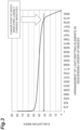
- FIG. 3 is a diagram showing a sorting result for the light-emitting elements according to the evaluation indices.
- a vertical axis represents an evaluation index according to the magnitude of the luminance
- a horizontal axis represents the order of the respective light-emitting elements.
- the evaluation index sharply decreases after a certain point (change point).
- the control apparatus 100 may determine that a light-emitting element having an evaluation index equal to or higher than the threshold value is a non-defective product (non-defective pixel), and a light-emitting element having an evaluation index smaller than the threshold value is a defective product (defective pixel).
- the threshold value may be determined by comparing a quality determination result for a light-emitting element based on fluorescence (photoluminescence) with a quality determination result based on probing (quality determination result based on an electrical characteristic).
- control apparatus 100 detects bright spots (fluorescence spots) in the light-emitting area of each light-emitting element based on the fluorescence image on the long wavelength side, and associates an address position with the number of bright spots for each light-emitting element.
- a bright spot (emission spot) on the long wavelength side of the normal emission spectrum is an abnormal emission point.
- the control apparatus 100 determines whether or not the fluorescence image on the long wavelength side contains a certain number or more of bright spots for a light-emitting element determined to be non-defective in the quality determination based on the fluorescence image having the original emission wavelength described above, and determines that a light-emitting element not containing the certain number or more of bright spots is a non-defective product (non-defective pixel) and a light-emitting element containing the certain number or more of bright spots is a defective product (defective pixel).
- a light-emitting element determined to be a non-defective product based on a fluorescence image having the original emission wavelength may be determined to be a defective product based on a fluorescence image on the long wavelength side.
- control apparatus 100 may determine the quality based on the fluorescence image on the long wavelength side acquired by the camera 81 for a light-emitting element determined to be defective by the determination. Further, the control apparatus 100 may determine the quality based on the fluorescence image on the long wavelength side for all the light-emitting elements.
- control apparatus 100 may determine the quality based on the fluorescence image on the long wavelength side only for a light-emitting element determined to be non-defective based on the fluorescence image having the original emission wavelength, determine the quality based on the fluorescence image on the long wavelength side only for a light-emitting element determined to be defective based on the fluorescence image having the original emission wavelength, or determine the quality based on the fluorescence image on the long wavelength side for all the light-emitting elements regardless of the quality determination result based on the fluorescence image having the original emission wavelength.
- the control apparatus 100 outputs the quality determination result for each light-emitting element. For example, the quality determination result is displayed on the monitor 110. Further, the control apparatus 100 may identify a defective portion (for example, a portion of a bright spot on the long wavelength side) in the light-emitting element, and output a position of the defective portion (so that the position is displayed on the monitor 110).
- a defective portion for example, a portion of a bright spot on the long wavelength side
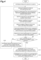
- FIG. 4 is a flowchart of the inspection method executed by the inspection apparatus 1.
- the irradiation region in the sample S is first determined (step S1). Specifically, the control apparatus 100 determines the irradiation region for excitation light by controlling the XY stage 12.
- the excitation light source 20 irradiates the irradiation region of the sample S with excitation light according to the control of the control apparatus 100 (step S2, excitation light irradiation step).
- the excitation light source 20 generates and emits light including a wavelength that excites the light-emitting element of the sample S.
- the excitation light reaches the dichroic mirror 40 via the optical fiber cable 31 and the light guide lens 32 of the optical system 30, is reflected by the dichroic mirror 40, and is concentrated on the irradiation region of the sample S via the objective lens 51.
- the light-emitting element of sample S emits fluorescence in response to excitation light.
- the fluorescence passes through the dichroic mirror 40 and is separated into fluorescence having the original emission wavelength and fluorescence on the long wavelength side in the dichroic mirror 60 (separation step).
- the fluorescence having the original emission wavelength forms an image by the imaging lens 72 and is guided to the camera 82.
- the fluorescence on the long wavelength side forms an image by the imaging lens 71 and is guided to the camera 81.
- the camera 81 images the fluorescence on the long wavelength side (step S3, first imaging step). Further, the camera 82 images the fluorescence having the original emission wavelength (step S3, second imaging step). The cameras 81 and 82 output fluorescence images, which are imaging results, to the control apparatus 100.
- the control apparatus 100 identifies the position of the light-emitting element based on the fluorescence images (step S4), and identifies the light-emitting area in each light-emitting element. Then, the control apparatus 100 derives a luminance (average luminance) in the light-emitting area of each light-emitting element based on the fluorescence image having the original emission wavelength (step S5). Further, the control apparatus 100 detects bright spots (fluorescence spots) in the light-emitting area of each light-emitting element based on the fluorescence image on the long wavelength side, and derives the number of bright spots (step S6). Then, the control apparatus 100 associates an address position with the luminance (average luminance) for each light-emitting element, and associates the address position with the number of bright spots (step S7).
- the control apparatus 100 derives an evaluation index from an absolute luminance and a relative luminance for each light-emitting element (step S8).
- the control apparatus 100 derives an evaluation index from, for example, the product of the absolute luminance and the relative luminance.
- the control apparatus 100 derives an evaluation index from the product of the absolute luminance and the relative luminance to the nth power (n is a natural number, for example, 2).
- control apparatus 100 determines whether or not the above-mentioned evaluation index has been derived for all the light-emitting elements (light-emitting elements to be determined) of the sample S (step S9).
- the control apparatus 100 determines a new irradiation region so that the light-emitting element before deriving the evaluation index is included (step S10). Thereafter, processing from step S2 is performed again.
- the control apparatus 100 determines the quality of each of the light-emitting elements by comparing the evaluation index of each light-emitting element with a predetermined threshold value (step S11, determination step). Specifically, the control apparatus 100 sorts (rearranges) the light-emitting elements in descending order of the evaluation indices, and determines that a light-emitting element having an evaluation index equal to or higher than the threshold value is a non-defective product (non-defective pixel), and a light-emitting element having an evaluation index smaller than the threshold value is a defective product (defective pixel).
- the control apparatus 100 determines the quality of each of the light-emitting elements by comparing the number of bright spots included in the fluorescence image on the long wavelength side with a predetermined threshold value (step S12, determination step). Specifically, the control apparatus 100 determines that a light-emitting element not containing a certain number or more of bright spots in the fluorescence image on the long wavelength side is a non-defective product (non-defective pixel), and a light-emitting element containing the certain number or more of bright spots is a defective product (defective pixel). The control apparatus 100 may output a quality determination result for each light-emitting element. Further, the control apparatus 100 may identify a defective portion (for example, a portion of a bright spot on the long wavelength side) in the light-emitting element and output a position of the defective portion (so that the position is displayed on the monitor 110).
- a defective portion for example, a portion of a bright spot on the long wavelength side
- the inspection apparatus 1 is an inspection apparatus for inspecting a sample S in which a plurality of light-emitting elements is formed, and includes an excitation light source 20 that generates excitation light to irradiate the sample S, a camera 81 that images fluorescence having a wavelength longer than a reference wavelength BW (see FIG.
- the control apparatus 100 determines the quality of the light-emitting element based on a fluorescence image (first fluorescence image) on the long wavelength side acquired by the camera 81, and the reference wavelength BW is a wavelength obtained by adding a full width at half maximum WH of a normal fluorescence spectrum ES of the light-emitting element to a peak wavelength PW of the normal fluorescence spectrum ES (see FIG. 2 ).
- the quality of the light-emitting element is determined based on a fluorescence image having a wavelength obtained by adding the full width at half maximum WH of the normal fluorescence spectrum ES of the light-emitting element to the peak wavelength PW of the normal fluorescence spectrum ES, that is, a fluorescence image on the long wavelength side that cannot be included in the normal fluorescence spectrum ES of the light-emitting element.
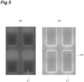
- FIG. 5 shows fluorescence images of a light-emitting element L1 in an abnormal light emission state, in which FIG. 5(a) is a fluorescence image having an original emission wavelength, and FIG. 5(b) is a fluorescence image on a long wavelength side. As shown in FIG.
- the light-emitting element L1 in the abnormal light emission state may have a fluorescence spot FP at longer wavelengths than the normal fluorescence spectrum.
- FIG. 6 is a diagram showing a luminance distribution of a light-emitting element in an abnormal light emission state and a luminance distribution of a light-emitting element in a normal light emission state.
- a vertical axis represents a luminance
- a horizontal axis represents a cumulative ratio.
- a light-emitting element in an abnormal light emission state has a smaller luminance than that of a light-emitting element in a normal light emission state.
- a light-emitting element in an abnormal light emission state in which a fluorescence spot is generated on the long wavelength side has a small luminance, and thus needs to be determined to be a defective product.
- the inspection apparatus 1 of the present embodiment when the quality of the light-emitting element is determined based on a fluorescence image on the long wavelength side, it is possible to appropriately detect the fluorescence spot on the long wavelength side described above, and appropriately determine that a light-emitting element having the fluorescence spot is defective. That is, according to the inspection apparatus 1, by considering the fluorescence on the long wavelength side, it is possible to determine the quality of the light-emitting element with high accuracy.
- the inspection apparatus 1 includes the dichroic mirror 60 that separates fluorescence from a light-emitting element into fluorescence on a long wavelength side and fluorescence having an original emission wavelength, and the camera 82 that images fluorescence, which has an original emission wavelength, having a wavelength included in a normal fluorescence spectrum of the light-emitting element.
- the dichroic mirror 60 that separates fluorescence from a light-emitting element into fluorescence on a long wavelength side and fluorescence having an original emission wavelength
- the camera 82 that images fluorescence, which has an original emission wavelength, having a wavelength included in a normal fluorescence spectrum of the light-emitting element.
- the control apparatus 100 determines the quality of the light-emitting element based on the fluorescence image on the long wavelength side and the fluorescence image having the original emission wavelength (second fluorescence image) acquired by the camera 82. In this way, in addition to determining the quality of the light-emitting element in consideration of the fluorescence on the long wavelength side, it is possible to determine the quality of the light-emitting element based on the fluorescence having the wavelength included in the normal fluorescence spectrum. In this way, it is possible to determine the quality of the light-emitting element with higher accuracy in consideration of both the abnormality (fluorescence spot) on the long wavelength side and the light emission state in the normal fluorescence spectrum.
- the control apparatus 100 may determine the quality of the light-emitting element based on the fluorescence image having the original emission wavelength, and determine the quality based on the fluorescence image on the long wavelength side for a light-emitting element determined to be non-defective in the determination after the determination.
- a light-emitting element whose light emission state in the normal fluorescence spectrum is abnormal is appropriately determined to be defective, it is possible to further determine that a light-emitting element, which has an abnormality (fluorescence spot) on the long wavelength side even though a light emission state in the normal fluorescence spectrum is normal, is defective, and it is possible to identify a defective light-emitting element without omission in consideration of both the light emission state on the long wavelength side and the light emission state in the normal fluorescence spectrum.
- the control apparatus 100 may determine the quality of the light-emitting element based on the fluorescence image having the original emission wavelength, and determine the quality based on the fluorescence image on the long wavelength side for a light-emitting element determined to be defective in the determination after the determination. According to such a configuration, for example, even when a light-emitting element is determined to be defective based on the light emission state in the normal fluorescence spectrum, if the light-emitting element has no abnormality (fluorescence spot) on the long wavelength side, the light-emitting element can be determined to be non-defective, and it is possible to prevent a light-emitting element not having a serious abnormality (fluorescence spot on the long wavelength side) from being determined to be defective.
- the quality determination based on the fluorescence image on the long wavelength side is performed only for a light-emitting element determined to be defective in the quality determination based on the fluorescence image having the original emission wavelength, it is possible to shorten a time required for determination related to an abnormality on the long wavelength side.
- the control apparatus 100 determines the quality of the light-emitting element based on the luminance of the fluorescence image having the original emission wavelength, and determines the quality of the light-emitting element based on the bright spot included in the fluorescence image on the long wavelength side. According to such a configuration, the quality of the light-emitting element can be determined with higher accuracy in consideration of the luminance of the fluorescence in the normal fluorescence spectrum and information about the fluorescence spot on the long wavelength side (presence or absence and the number of abnormal fluorescence spots, etc.).
- the control apparatus 100 outputs a quality determination result for each light-emitting element. In this way, it is possible to identify a light-emitting element that affects the light emission efficiency and take measures to improve the light emission efficiency by using the quality determination result for each light-emitting element.
- the control apparatus 100 identifies a defective portion in the light-emitting element, and outputs a position of the defective portion. For example, when a position of a fluorescence spot on the long wavelength side in the light-emitting element is identified based on an imaging result, and the position of the fluorescence spot is output as a defective portion, it is possible to take measures to improve the light emission efficiency based on information about the defective portion.
- the invention is not limited to the embodiment.
- the first wavelength and the second wavelength have been described as being the same wavelength (reference wavelength BW)
- the wavelengths are not limited thereto and may be different from each other.
- the control apparatus 100 may determine the quality of the light-emitting element based only on the fluorescence on the long wavelength side imaged by the camera 81.
- the inspection apparatus 1A may not have a configuration for acquiring the fluorescence having the original emission wavelength (the dichroic mirror 60, the camera 82, and the imaging lens 72 illustrated in FIG. 1 ).
- the quality determination for the light-emitting element based on the fluorescence on the long wavelength side a description has been given on the assumption that it is determined whether or not the fluorescence image contains a certain number or more of bright spots.
- the invention is not limited thereto, and the quality of the light-emitting element may be determined simply depending on whether or not the fluorescence image contains one or more bright spots.
- the invention is not limited to using a dichroic mirror having such a characteristic.
- the transmittance (reflectance) of the fluorescence changes according to the change in wavelength in a specific wavelength band, and the transmittance (reflectance) of the fluorescence is constant regardless of the change in wavelength in a wavelength band other than the specific wavelength band (lower wavelength side of the specific wavelength band and higher wavelength side of the specific wavelength band).
- the width of the wavelength band in which the transmittance (reflectance) of the fluorescence changes according to the change in wavelength is defined as an "edge shift width"
- the edge shift width of such a dichroic mirror may be made wider than the full width at half maximum of the normal fluorescence spectrum of the light-emitting element.
- 1, 1A inspection apparatus
- 20 excitation light source
- 60 dichroic mirror (optical element)
- 81 camera (first imaging unit)
- 82 camera (second imaging unit)
- 100 control apparatus (determining unit).
Landscapes
- Health & Medical Sciences (AREA)
- Physics & Mathematics (AREA)
- General Physics & Mathematics (AREA)
- Immunology (AREA)
- Chemical & Material Sciences (AREA)
- Life Sciences & Earth Sciences (AREA)
- Biochemistry (AREA)
- General Health & Medical Sciences (AREA)
- Analytical Chemistry (AREA)
- Pathology (AREA)
- Engineering & Computer Science (AREA)
- Nuclear Medicine, Radiotherapy & Molecular Imaging (AREA)
- Computer Vision & Pattern Recognition (AREA)
- Signal Processing (AREA)
- Manufacturing & Machinery (AREA)
- Power Engineering (AREA)
- Microelectronics & Electronic Packaging (AREA)
- Computer Hardware Design (AREA)
- Optics & Photonics (AREA)
- Theoretical Computer Science (AREA)
- Quality & Reliability (AREA)
- Chemical Kinetics & Catalysis (AREA)
- Condensed Matter Physics & Semiconductors (AREA)
- Investigating, Analyzing Materials By Fluorescence Or Luminescence (AREA)
- Testing Of Optical Devices Or Fibers (AREA)
- Testing Or Measuring Of Semiconductors Or The Like (AREA)
Applications Claiming Priority (2)
| Application Number | Priority Date | Filing Date | Title |
|---|---|---|---|
| JP2019062971 | 2019-03-28 | ||
| PCT/JP2020/003248 WO2020195136A1 (ja) | 2019-03-28 | 2020-01-29 | 検査装置及び検査方法 |
Publications (3)
| Publication Number | Publication Date |
|---|---|
| EP3951845A1 EP3951845A1 (en) | 2022-02-09 |
| EP3951845A4 EP3951845A4 (en) | 2022-12-07 |
| EP3951845B1 true EP3951845B1 (en) | 2025-06-25 |
Family
ID=72610001
Family Applications (1)
| Application Number | Title | Priority Date | Filing Date |
|---|---|---|---|
| EP20780030.1A Active EP3951845B1 (en) | 2019-03-28 | 2020-01-29 | Inspection device and inspection method |
Country Status (7)
Families Citing this family (8)
| Publication number | Priority date | Publication date | Assignee | Title |
|---|---|---|---|---|
| CN116978806A (zh) | 2019-03-28 | 2023-10-31 | 浜松光子学株式会社 | 检查装置及检查方法 |
| JP6746744B1 (ja) * | 2019-03-28 | 2020-08-26 | 浜松ホトニクス株式会社 | 検査装置及び検査方法 |
| JP7374937B2 (ja) * | 2021-01-13 | 2023-11-07 | 株式会社アドバンテスト | 試験装置、試験方法およびプログラム |
| JP7386190B2 (ja) | 2021-01-21 | 2023-11-24 | 株式会社アドバンテスト | 試験装置、試験方法およびプログラム |
| JP7629742B2 (ja) * | 2021-02-10 | 2025-02-14 | 浜松ホトニクス株式会社 | 検査装置及び検査方法 |
| JP7355773B2 (ja) | 2021-02-26 | 2023-10-03 | 株式会社アドバンテスト | 試験装置、試験方法およびプログラム |
| JP7355789B2 (ja) * | 2021-09-08 | 2023-10-03 | 株式会社アドバンテスト | 試験装置、試験方法およびプログラム |
| WO2024176621A1 (ja) * | 2023-02-24 | 2024-08-29 | 浜松ホトニクス株式会社 | 画像取得装置 |
Family Cites Families (20)
| Publication number | Priority date | Publication date | Assignee | Title |
|---|---|---|---|---|
| JPS63250835A (ja) * | 1987-04-08 | 1988-10-18 | Hitachi Cable Ltd | エピタキシヤルウエハの検査方法 |
| GB2231958A (en) | 1989-04-07 | 1990-11-28 | Hamamatsu Photonics Kk | Measuring fluorescence characteristics |
| EP2072947B1 (en) | 2007-08-07 | 2016-03-16 | Panasonic Intellectual Property Management Co., Ltd. | Image processing device and image processing method |
| JP2010118668A (ja) | 2009-12-11 | 2010-05-27 | Sumitomo Electric Ind Ltd | 化合物半導体部材のダメージ評価方法、化合物半導体部材の製造方法、窒化ガリウム系化合物半導体部材及び窒化ガリウム系化合物半導体膜 |
| US9163987B2 (en) * | 2010-08-24 | 2015-10-20 | Kla-Tencor Corporation | Defect inspection and photoluminescence measurement system |
| JP5963453B2 (ja) | 2011-03-15 | 2016-08-03 | 株式会社荏原製作所 | 検査装置 |
| CN103765567A (zh) | 2011-06-24 | 2014-04-30 | 科磊股份有限公司 | 使用光致发光成像检验发光半导体装置的方法和设备 |
| US8604447B2 (en) * | 2011-07-27 | 2013-12-10 | Kla-Tencor Corporation | Solar metrology methods and apparatus |
| JP6119273B2 (ja) * | 2013-01-31 | 2017-04-26 | 日亜化学工業株式会社 | 半導体発光素子の検査方法及び半導体発光素子の製造方法 |
| JP6051917B2 (ja) * | 2013-02-18 | 2016-12-27 | 日亜化学工業株式会社 | 半導体発光素子の検査方法及び半導体発光素子の製造方法 |
| JP6076133B2 (ja) | 2013-02-27 | 2017-02-08 | 東レエンジニアリング株式会社 | 蛍光発光体の検査装置 |
| JP2015010834A (ja) * | 2013-06-26 | 2015-01-19 | 東レエンジニアリング株式会社 | 発光体の発光波長推定方法とその装置 |
| JP6252598B2 (ja) * | 2013-12-09 | 2017-12-27 | 株式会社ニコン | 光学装置、測定装置、測定方法、スクリーニング装置及びスクリーニング方法 |
| CN103654730B (zh) | 2013-12-19 | 2016-04-20 | 北京大学 | 一种基于led光源的荧光分子成像系统及其成像方法 |
| WO2016187564A1 (en) | 2015-05-20 | 2016-11-24 | Quantum-Si Incorporated | Pulsed laser and bioanalytic system |
| KR102592917B1 (ko) | 2016-08-26 | 2023-10-23 | 삼성전자주식회사 | 표면 검사 방법 및 반도체 소자의 제조 방법 |
| JP2018132308A (ja) | 2017-02-13 | 2018-08-23 | 東レエンジニアリング株式会社 | 分光測定装置および発光体の発光波長推定装置 |
| CN112166314A (zh) * | 2018-05-30 | 2021-01-01 | 索尼公司 | 荧光观察设备和荧光观察方法 |
| JP7229729B2 (ja) * | 2018-11-08 | 2023-02-28 | 株式会社ディスコ | Facet領域の検出方法および検出装置ならびにウエーハの生成方法およびレーザー加工装置 |
| CN116978806A (zh) * | 2019-03-28 | 2023-10-31 | 浜松光子学株式会社 | 检查装置及检查方法 |
-
2020
- 2020-01-29 CN CN202080025090.3A patent/CN113632211B/zh active Active
- 2020-01-29 KR KR1020217028889A patent/KR20210144683A/ko active Pending
- 2020-01-29 WO PCT/JP2020/003248 patent/WO2020195136A1/ja active IP Right Grant
- 2020-01-29 US US17/442,158 patent/US12072289B2/en active Active
- 2020-01-29 CN CN202410512574.0A patent/CN118398511A/zh active Pending
- 2020-01-29 EP EP20780030.1A patent/EP3951845B1/en active Active
- 2020-03-17 TW TW109108722A patent/TWI831946B/zh active
- 2020-03-17 TW TW113103846A patent/TWI866767B/zh active
- 2020-06-17 JP JP2020104552A patent/JP7535391B2/ja active Active
-
2024
- 2024-07-08 US US18/766,095 patent/US20240361244A1/en active Pending
Also Published As
| Publication number | Publication date |
|---|---|
| TWI831946B (zh) | 2024-02-11 |
| TW202043745A (zh) | 2020-12-01 |
| CN113632211A (zh) | 2021-11-09 |
| US20240361244A1 (en) | 2024-10-31 |
| US20220178837A1 (en) | 2022-06-09 |
| KR20210144683A (ko) | 2021-11-30 |
| WO2020195136A1 (ja) | 2020-10-01 |
| EP3951845A4 (en) | 2022-12-07 |
| TWI866767B (zh) | 2024-12-11 |
| CN118398511A (zh) | 2024-07-26 |
| EP3951845A1 (en) | 2022-02-09 |
| JP7535391B2 (ja) | 2024-08-16 |
| CN113632211B (zh) | 2024-05-17 |
| TW202422050A (zh) | 2024-06-01 |
| US12072289B2 (en) | 2024-08-27 |
| JP2020167433A (ja) | 2020-10-08 |
Similar Documents
| Publication | Publication Date | Title |
|---|---|---|
| EP3951845B1 (en) | Inspection device and inspection method | |
| US12387309B2 (en) | Inspection apparatus and inspection method | |
| US12405228B2 (en) | Inspection apparatus and inspection method | |
| US20250155374A1 (en) | Inspection apparatus and inspection method | |
| JP6720429B1 (ja) | 検査装置及び検査方法 | |
| JP2020177032A (ja) | 検査装置及び検査方法 | |
| JP6720430B1 (ja) | 検査装置及び検査方法 | |
| JP2022122596A (ja) | 検査装置及び検査方法 |
Legal Events
| Date | Code | Title | Description |
|---|---|---|---|
| STAA | Information on the status of an ep patent application or granted ep patent |
Free format text: STATUS: THE INTERNATIONAL PUBLICATION HAS BEEN MADE |
|
| PUAI | Public reference made under article 153(3) epc to a published international application that has entered the european phase |
Free format text: ORIGINAL CODE: 0009012 |
|
| STAA | Information on the status of an ep patent application or granted ep patent |
Free format text: STATUS: REQUEST FOR EXAMINATION WAS MADE |
|
| 17P | Request for examination filed |
Effective date: 20210727 |
|
| AK | Designated contracting states |
Kind code of ref document: A1 Designated state(s): AL AT BE BG CH CY CZ DE DK EE ES FI FR GB GR HR HU IE IS IT LI LT LU LV MC MK MT NL NO PL PT RO RS SE SI SK SM TR |
|
| DAV | Request for validation of the european patent (deleted) | ||
| DAX | Request for extension of the european patent (deleted) | ||
| A4 | Supplementary search report drawn up and despatched |
Effective date: 20221109 |
|
| RIC1 | Information provided on ipc code assigned before grant |
Ipc: H01L 33/00 20100101ALI20221103BHEP Ipc: G01N 21/956 20060101ALI20221103BHEP Ipc: G01N 21/95 20060101ALI20221103BHEP Ipc: G01N 21/88 20060101ALI20221103BHEP Ipc: G01N 21/64 20060101ALI20221103BHEP Ipc: H01L 21/66 20060101AFI20221103BHEP |
|
| REG | Reference to a national code |
Ref country code: DE Ref legal event code: R079 Free format text: PREVIOUS MAIN CLASS: H01L0021660000 Ipc: G01N0021640000 Ref country code: DE Ref legal event code: R079 Ref document number: 602020053374 Country of ref document: DE Free format text: PREVIOUS MAIN CLASS: H01L0021660000 Ipc: G01N0021640000 |
|
| GRAP | Despatch of communication of intention to grant a patent |
Free format text: ORIGINAL CODE: EPIDOSNIGR1 |
|
| STAA | Information on the status of an ep patent application or granted ep patent |
Free format text: STATUS: GRANT OF PATENT IS INTENDED |
|
| RIC1 | Information provided on ipc code assigned before grant |
Ipc: G01N 21/95 20060101ALI20250312BHEP Ipc: G01N 21/956 20060101ALI20250312BHEP Ipc: G01N 21/88 20060101ALI20250312BHEP Ipc: G01N 21/64 20060101AFI20250312BHEP |
|
| INTG | Intention to grant announced |
Effective date: 20250325 |
|
| GRAS | Grant fee paid |
Free format text: ORIGINAL CODE: EPIDOSNIGR3 |
|
| GRAA | (expected) grant |
Free format text: ORIGINAL CODE: 0009210 |
|
| STAA | Information on the status of an ep patent application or granted ep patent |
Free format text: STATUS: THE PATENT HAS BEEN GRANTED |
|
| AK | Designated contracting states |
Kind code of ref document: B1 Designated state(s): AL AT BE BG CH CY CZ DE DK EE ES FI FR GB GR HR HU IE IS IT LI LT LU LV MC MK MT NL NO PL PT RO RS SE SI SK SM TR |
|
| REG | Reference to a national code |
Ref country code: GB Ref legal event code: FG4D |
|
| REG | Reference to a national code |
Ref country code: CH Ref legal event code: EP |
|
| REG | Reference to a national code |
Ref country code: CH Ref legal event code: EP |
|
| REG | Reference to a national code |
Ref country code: IE Ref legal event code: FG4D |
|
| REG | Reference to a national code |
Ref country code: DE Ref legal event code: R096 Ref document number: 602020053374 Country of ref document: DE |
|
| REG | Reference to a national code |
Ref country code: NL Ref legal event code: FP |
|
| P01 | Opt-out of the competence of the unified patent court (upc) registered |
Free format text: CASE NUMBER: UPC_APP_1549_3951845/2025 Effective date: 20250730 |