EP3951448B1 - Display body - Google Patents
Display body Download PDFInfo
- Publication number
- EP3951448B1 EP3951448B1 EP20777415.9A EP20777415A EP3951448B1 EP 3951448 B1 EP3951448 B1 EP 3951448B1 EP 20777415 A EP20777415 A EP 20777415A EP 3951448 B1 EP3951448 B1 EP 3951448B1
- Authority
- EP
- European Patent Office
- Prior art keywords
- recess
- display
- multilayer film
- light
- angle
- Prior art date
- Legal status (The legal status is an assumption and is not a legal conclusion. Google has not performed a legal analysis and makes no representation as to the accuracy of the status listed.)
- Active
Links
Images


Classifications
-
- B—PERFORMING OPERATIONS; TRANSPORTING
- B32—LAYERED PRODUCTS
- B32B—LAYERED PRODUCTS, i.e. PRODUCTS BUILT-UP OF STRATA OF FLAT OR NON-FLAT, e.g. CELLULAR OR HONEYCOMB, FORM
- B32B3/00—Layered products comprising a layer with external or internal discontinuities or unevennesses, or a layer of non-planar shape; Layered products comprising a layer having particular features of form
- B32B3/26—Layered products comprising a layer with external or internal discontinuities or unevennesses, or a layer of non-planar shape; Layered products comprising a layer having particular features of form characterised by a particular shape of the outline of the cross-section of a continuous layer; characterised by a layer with cavities or internal voids ; characterised by an apertured layer
- B32B3/30—Layered products comprising a layer with external or internal discontinuities or unevennesses, or a layer of non-planar shape; Layered products comprising a layer having particular features of form characterised by a particular shape of the outline of the cross-section of a continuous layer; characterised by a layer with cavities or internal voids ; characterised by an apertured layer characterised by a layer formed with recesses or projections, e.g. hollows, grooves, protuberances, ribs
-
- B—PERFORMING OPERATIONS; TRANSPORTING
- B32—LAYERED PRODUCTS
- B32B—LAYERED PRODUCTS, i.e. PRODUCTS BUILT-UP OF STRATA OF FLAT OR NON-FLAT, e.g. CELLULAR OR HONEYCOMB, FORM
- B32B7/00—Layered products characterised by the relation between layers; Layered products characterised by the relative orientation of features between layers, or by the relative values of a measurable parameter between layers, i.e. products comprising layers having different physical, chemical or physicochemical properties; Layered products characterised by the interconnection of layers
- B32B7/02—Physical, chemical or physicochemical properties
- B32B7/023—Optical properties
-
- B—PERFORMING OPERATIONS; TRANSPORTING
- B32—LAYERED PRODUCTS
- B32B—LAYERED PRODUCTS, i.e. PRODUCTS BUILT-UP OF STRATA OF FLAT OR NON-FLAT, e.g. CELLULAR OR HONEYCOMB, FORM
- B32B9/00—Layered products comprising a layer of a particular substance not covered by groups B32B11/00 - B32B29/00
-
- B—PERFORMING OPERATIONS; TRANSPORTING
- B32—LAYERED PRODUCTS
- B32B—LAYERED PRODUCTS, i.e. PRODUCTS BUILT-UP OF STRATA OF FLAT OR NON-FLAT, e.g. CELLULAR OR HONEYCOMB, FORM
- B32B9/00—Layered products comprising a layer of a particular substance not covered by groups B32B11/00 - B32B29/00
- B32B9/04—Layered products comprising a layer of a particular substance not covered by groups B32B11/00 - B32B29/00 comprising such particular substance as the main or only constituent of a layer, which is next to another layer of the same or of a different material
-
- B—PERFORMING OPERATIONS; TRANSPORTING
- B42—BOOKBINDING; ALBUMS; FILES; SPECIAL PRINTED MATTER
- B42D—BOOKS; BOOK COVERS; LOOSE LEAVES; PRINTED MATTER CHARACTERISED BY IDENTIFICATION OR SECURITY FEATURES; PRINTED MATTER OF SPECIAL FORMAT OR STYLE NOT OTHERWISE PROVIDED FOR; DEVICES FOR USE THEREWITH AND NOT OTHERWISE PROVIDED FOR; MOVABLE-STRIP WRITING OR READING APPARATUS
- B42D25/00—Information-bearing cards or sheet-like structures characterised by identification or security features; Manufacture thereof
- B42D25/30—Identification or security features, e.g. for preventing forgery
- B42D25/328—Diffraction gratings; Holograms
-
- B—PERFORMING OPERATIONS; TRANSPORTING
- B42—BOOKBINDING; ALBUMS; FILES; SPECIAL PRINTED MATTER
- B42D—BOOKS; BOOK COVERS; LOOSE LEAVES; PRINTED MATTER CHARACTERISED BY IDENTIFICATION OR SECURITY FEATURES; PRINTED MATTER OF SPECIAL FORMAT OR STYLE NOT OTHERWISE PROVIDED FOR; DEVICES FOR USE THEREWITH AND NOT OTHERWISE PROVIDED FOR; MOVABLE-STRIP WRITING OR READING APPARATUS
- B42D25/00—Information-bearing cards or sheet-like structures characterised by identification or security features; Manufacture thereof
- B42D25/40—Manufacture
- B42D25/405—Marking
- B42D25/43—Marking by removal of material
- B42D25/435—Marking by removal of material using electromagnetic radiation, e.g. laser
-
- B—PERFORMING OPERATIONS; TRANSPORTING
- B42—BOOKBINDING; ALBUMS; FILES; SPECIAL PRINTED MATTER
- B42D—BOOKS; BOOK COVERS; LOOSE LEAVES; PRINTED MATTER CHARACTERISED BY IDENTIFICATION OR SECURITY FEATURES; PRINTED MATTER OF SPECIAL FORMAT OR STYLE NOT OTHERWISE PROVIDED FOR; DEVICES FOR USE THEREWITH AND NOT OTHERWISE PROVIDED FOR; MOVABLE-STRIP WRITING OR READING APPARATUS
- B42D25/00—Information-bearing cards or sheet-like structures characterised by identification or security features; Manufacture thereof
- B42D25/40—Manufacture
- B42D25/45—Associating two or more layers
- B42D25/455—Associating two or more layers using heat
-
- B—PERFORMING OPERATIONS; TRANSPORTING
- B42—BOOKBINDING; ALBUMS; FILES; SPECIAL PRINTED MATTER
- B42D—BOOKS; BOOK COVERS; LOOSE LEAVES; PRINTED MATTER CHARACTERISED BY IDENTIFICATION OR SECURITY FEATURES; PRINTED MATTER OF SPECIAL FORMAT OR STYLE NOT OTHERWISE PROVIDED FOR; DEVICES FOR USE THEREWITH AND NOT OTHERWISE PROVIDED FOR; MOVABLE-STRIP WRITING OR READING APPARATUS
- B42D25/00—Information-bearing cards or sheet-like structures characterised by identification or security features; Manufacture thereof
- B42D25/40—Manufacture
- B42D25/45—Associating two or more layers
- B42D25/46—Associating two or more layers using pressure
-
- G—PHYSICS
- G02—OPTICS
- G02B—OPTICAL ELEMENTS, SYSTEMS OR APPARATUS
- G02B5/00—Optical elements other than lenses
- G02B5/18—Diffraction gratings
- G02B5/1814—Diffraction gratings structurally combined with one or more further optical elements, e.g. lenses, mirrors, prisms or other diffraction gratings
-
- G—PHYSICS
- G02—OPTICS
- G02B—OPTICAL ELEMENTS, SYSTEMS OR APPARATUS
- G02B5/00—Optical elements other than lenses
- G02B5/18—Diffraction gratings
- G02B5/1861—Reflection gratings characterised by their structure, e.g. step profile, contours of substrate or grooves, pitch variations, materials
-
- G—PHYSICS
- G02—OPTICS
- G02B—OPTICAL ELEMENTS, SYSTEMS OR APPARATUS
- G02B5/00—Optical elements other than lenses
- G02B5/20—Filters
- G02B5/28—Interference filters
- G02B5/285—Interference filters comprising deposited thin solid films
-
- B—PERFORMING OPERATIONS; TRANSPORTING
- B32—LAYERED PRODUCTS
- B32B—LAYERED PRODUCTS, i.e. PRODUCTS BUILT-UP OF STRATA OF FLAT OR NON-FLAT, e.g. CELLULAR OR HONEYCOMB, FORM
- B32B2307/00—Properties of the layers or laminate
- B32B2307/40—Properties of the layers or laminate having particular optical properties
- B32B2307/412—Transparent
-
- B—PERFORMING OPERATIONS; TRANSPORTING
- B32—LAYERED PRODUCTS
- B32B—LAYERED PRODUCTS, i.e. PRODUCTS BUILT-UP OF STRATA OF FLAT OR NON-FLAT, e.g. CELLULAR OR HONEYCOMB, FORM
- B32B2307/00—Properties of the layers or laminate
- B32B2307/40—Properties of the layers or laminate having particular optical properties
- B32B2307/416—Reflective
-
- B—PERFORMING OPERATIONS; TRANSPORTING
- B32—LAYERED PRODUCTS
- B32B—LAYERED PRODUCTS, i.e. PRODUCTS BUILT-UP OF STRATA OF FLAT OR NON-FLAT, e.g. CELLULAR OR HONEYCOMB, FORM
- B32B2307/00—Properties of the layers or laminate
- B32B2307/40—Properties of the layers or laminate having particular optical properties
- B32B2307/418—Refractive
-
- B—PERFORMING OPERATIONS; TRANSPORTING
- B32—LAYERED PRODUCTS
- B32B—LAYERED PRODUCTS, i.e. PRODUCTS BUILT-UP OF STRATA OF FLAT OR NON-FLAT, e.g. CELLULAR OR HONEYCOMB, FORM
- B32B2457/00—Electrical equipment
- B32B2457/20—Displays, e.g. liquid crystal displays, plasma displays
Definitions
- the present invention relates to a display.
- Holograms which are difficult to counterfeit or replicate are conventionally used to prove articles as being genuine products. For example, attachment of a transparent film equipped with a hologram to a card recorded with a personal information such as a facial image protects the personal information from being altered. In addition, using holograms in banknotes or securities prevent their unauthorized duplication. In recent years, recording a facial image using a hologram on an ID (identification) card or the like has also been proposed (PTL 1 and 2).
- PTL 3 describes forgery prevention medium wherein at least a diffraction structure forming layer, an intermediate layer and a first reflection layer are laminated in the order on a support, a diffraction structure region is formed on part of the intermediate layer side of the diffraction structure forming layer, and a second reflection layer is further formed on part of the diffraction structure region.
- PTL 4 describes a diffraction structure is constituted by laminating a plurality of diffraction structure forming layers having different diffraction structures on one surface of a transparent base and laminating four layers including the first diffraction structure forming layer provided with an embossed face being at least the diffraction structure, a light reflecting layer, the second diffraction structure forming layer provided with an embossed face being the diffraction structure being different from the first diffraction structure forming layer, and a light reflecting layer in this order.
- PTL 5 describes a display comprising a first optical effect layer (12) including a first interface part, a reflective material layer covering at least a part of the first interface part, and a second optical effect layer including, at a position of a first portion of the first interface part (IF 1) that is covered with the reflective material.
- PTL 6 describes a multilayer color film provided to replace a complicated fluorescent material or a color filter in a color display by illuminating a variety of colors by differentiating thicknesses at separate regions.
- PTL 7 describes asecurity device including a liquid crystal layer which is made of solidified liquid crystal material.
- holograms which are difficult to counterfeit or duplicate have been used in various articles for which it is desired to prevent their unauthorized duplication.
- An object of the present invention is to provide a technique for manufacturing a display for displaying an image by structural color in a decreased time.
- visible range means a wavelength range of 350 nm to 750 nm.
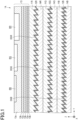
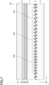
- Fig. 1 is a schematic cross-sectional view illustrating a display according to a first embodiment of the present invention.
- a display 1A includes a multilayer film 13, front layers 11R, 11G and 11B, reflective layers 12R, 12G and 12B, and back layers 14R, 14G and 14B.
- the surface of the display 1A on the multilayer film 13 side is a front surface
- the back surface thereof is a back surface.
- a surface closer to the front surface of the display 1A is referred to as a front surface
- a surface closer to the back surface of the display 1A is referred to as a back surface.
- the multilayer film 13 is a dielectric multilayer film including a laminate formed of at least two dielectric layers having refractive indices different from each other.
- the multilayer film 13 is composed of a laminate formed by alternately laminating dielectric layers 13a and 13b having refractive indices different from each other.
- the multilayer film 13 may further include a protective layer which covers the front surface of the laminate.
- the protective layer may have a monolayer structure, or may have a multilayer structure.
- each layer constituting the multilayer film 13 may be, for example, in the range of 5 nm or more and 500 um or less.
- Materials that can be used for each layer constituting the multilayer film 13 may be, for example, transparent dielectric materials such as zinc sulfide and titanium dioxide.
- the multilayer film 13 is formed of two kinds of dielectric layers 13a and 13b having refractive indices (materials) different from each other.
- the multilayer film 13 may be formed of three or more dielectric layers having refractive indices (materials) different from each other.
- the laminate has formed in the front surface thereof, a first recess RR, a second recess RG, and a third recess RB, as at least one recess.
- the first recess RR, the second recess RG, and the third recess RB are arranged in one of the dielectric layers 13a which is located closest to the front surface of the laminate.
- the third recess RB may be omitted.
- the second recess RG may also be omitted.
- the first recess RR, the second recess RG, and the third recess RB have depths different from each other. Although the first recess RR, the second recess RG, and the third recess RB are increasingly shallow in depth in this order, any of them may be the shallowest, or any of them may be the deepest.
- one of the dielectric layers 13a, located closest to the front surface of the laminate is drawn thicker than the other dielectric layers 13a and 13b, for ease of understanding the difference in depths of the recesses.
- One of the dielectric layers 13a, located closest to the front surface of the laminate may have the same thickness as, or may be thinner than, any of the other dielectric layers 13a and 13b.
- a portion of the multilayer film 13 where there is no recess shows, for example, a high transmittance over the entire visible range or a low transmittance over the entire visible range.
- white light refers to light having substantially equal intensity over the entire visible range.
- the multilayer film 13 includes a first portion aligned with the first recess RR, a second portion aligned with the second recess RG, a third portion aligned with the third recess RB, and portions having no recesses, and all the portions show transmission spectra different from each other when white light is made incident at the first angle of incidence.
- the first to third portions have wavelengths of maximum or minimum transmittance in the visible range that are different from each other when white light is made incident on the portions at the first angle of incidence.
- a transmission spectrum of white light which is made incident at the first angle of incidence on the multilayer film 13, shows a ratio of transmittance in a first wavelength range to transmittance in other wavelength ranges being larger in the first portion of the multilayer film 13 aligned with the first recess RR than in the portions of the multilayer film 13 without any recess, and shows a maximum transmittance at the first wavelength in the first wavelength range.
- the transmission spectrum of white light made incident on the multilayer film 13 at the first angle of incidence shows, for example, a ratio of transmittance in a second wavelength range to transmittance in other wavelength ranges being larger in the second portion of the multilayer film 13 aligned with the second recess RG than in the portions without any recess, and shows a maximum transmittance at the second wavelength in the second wavelength range.
- the transmission spectrum of white light made incident on the multilayer film 13 at the first angle of incidence shows a ratio of transmittance in the first wavelength range to transmittance in other wavelength ranges being smaller in the first portion of the multilayer film 13 aligned with the first recess RR than in the portions without any recess, and shows a minimum transmittance at the first wavelength in the first wavelength range.
- the transmission spectrum of white light made incident on the multilayer film 13 at the first angle of incidence shows, for example, a ratio of transmittance in the second wavelength range to transmittance in other wavelength ranges being smaller in the second portion of the multilayer film 13 aligned with the second recess RG than in the portions without any recess, and shows a minimum transmittance at the second wavelength in the second wavelength range.
- the transmission spectrum of white light made incident on the multilayer film 13 at the first angle of incidence shows, for example, a ratio of transmittance in the third wavelength range to transmittance in other wavelength ranges being smaller in the third portion of the multilayer film 13 aligned with the third recess RB than in the portions without any recess, and shows a minimum transmittance at the third wavelength in the third wavelength range.
- the multilayer film 13 adopts the former configuration.
- the first to third wavelength ranges are wavelength ranges different from each other, in the visible range.
- the longest wavelength in the second wavelength range is shorter than the shortest wavelength in the first wavelength range
- the longest wavelength in the third wavelength range is shorter than the shortest wavelength in the second wavelength range.
- the first, second, and third wavelength ranges are red, green, and blue wavelength ranges, respectively.
- the front layer 11R, the reflective layer 12R, and the back layer 14R are laminated on the back surface of the multilayer film 13 in this order.
- a front layer 11G, a reflective layer 12G, and a back layer 14G are laminated on the back layer 14R in this order.
- a front layer 11B, a reflective layer 12B and a back layer 14B are laminated on the back layer 14G in this order.
- Each of the front layers 11R, 11G and 11B may be made of, for example, a transparent resin.
- the transparent resin may be a cured product of a thermosetting resin or a photocurable resin, a thermoplastic resin, an adhesive or a pressure sensitive adhesive.
- Each of these layers may have a monolayer structure, or may have a multilayer structure.
- the back surfaces of the front layers 11R, 11G, and 11B are provided with the first, second, and third relief structures, respectively.
- the first, second, and third relief structures each allow the first reflective surface, which is the interface between the front layer 11R and the reflective layer 12R, the second reflective surface, which is the interface between the front layer 11G and the reflective layer 12G, and the third reflective surface, which is the interface between the front layer 11B and the reflective layer 12B to direct light, which has entered the multilayer film 13 as white light at a first angle of incidence and then emerged at an angle of emergence from the back surface of the multilayer film 13, to be incident on the back surface of the multilayer film 13 at a second angle of incidence which is different from the angle of emergence of the light.
- the first relief structure forms a first blazed diffraction grating on the first reflective surface
- the second relief structure forms a second blazed diffraction grating on the second reflective surface
- the third relief structure forms a third blazed diffraction grating on the third reflective surface.
- the first to third blazed diffraction gratings are parallel to each other in the arrangement direction of grooves or edges constituting them. The arrangement direction of the grooves or edges is parallel to the Y direction.
- the first to third blazed diffraction gratings have spatial frequencies of the grating lines different from each other.
- the first blazed diffraction grating has the lowest spatial frequency of grating lines
- the third blazed diffraction grating has the highest spatial frequency of grating lines.
- the magnitude relationship of the spatial frequencies of the grating lines between the first to third blazed diffraction gratings may be different from the above.
- the first blazed diffraction grating has a defined blaze angle and a defined grating constant (line spacing) so that when white light is made incident on the multilayer film 13 at the first angle of incidence, the light (light at the first wavelength) transmitted through the first portion of the multilayer film 13 aligned with the first recess RR is made incident again on the multilayer film 13 at the second angle of incidence.
- the spatial frequency of grating lines constituting the first blazed diffraction grating may be set in the range of, for example, 950 lines/mm to 2050 lines/mm.
- the blaze angle of the first blazed diffraction grating may be, for example, in the range of 1° to 89°.
- the second blazed diffraction grating has a defined blaze angle and a defined grating constant so that when white light is made incident on the multilayer film 13 at the first angle of incidence, the light (light at the second wavelength) transmitted through the second portion of the multilayer film 13 aligned with the second recess RG is made incident again on the multilayer film 13 at the second angle of incidence.
- the spatial frequency of grating lines constituting the second blazed diffraction grating may be set in the range of, for example, 950 lines/mm to 2050 lines/mm.
- the blaze angle of the second blazed diffraction grating may be made equal to, for example, the blaze angle of the first blazed diffraction grating.
- the third blazed diffraction grating has a defined blaze angle and a defined grating constant so that when white light is made incident on the multilayer film 13 at the first angle of incidence, the light (light at the third wavelength) transmitted through the third portion of the multilayer film 13 aligned with the third recess RB is made incident again on the multilayer film 13 at the second angle of incidence.
- the spatial frequency of grating lines constituting the third blazed diffraction grating may be set in the range of, for example, 950 lines/mm to 2050 lines/mm.
- the blaze angle of the third blazed diffraction grating may be made equal to, for example, the blaze angle of the first blazed diffraction grating.
- the structure formed at the interfaces by the first to third relief structures may be a diffraction grating other than a blazed diffraction grating.
- the structure formed at the interfaces by the first to third relief structures is a diffraction grating other than a blazed diffraction grating
- the grating constants of the diffraction gratings may be, for example, within the range described above for the blazed diffraction grating.
- the structure in which the first to third relief structures are formed at the above interfaces does not necessarily have to have a function as a diffraction grating, as long as the structure is capable of allowing light that has been transmitted through the multilayer film 13 to enter the multilayer film 13 again at the second angle of incidence.
- the reflective layers 12R, 12G, and 12B each cover the back surface of the front layers 11R, 11G, and 11B.
- the reflective layers 12R and 12G are made of transparent materials.
- the reflective layers 12R and 12G each have refractive indices different from those of the front layers 11R and 11G.
- the materials exemplified for the dielectric layers 13a and 13b may be used.
- the reflective layer 12B is made of a transparent material or an opaque material. In a case in which the reflective layer 12B is made of a transparent material, its refractive index is different from that of the front layer 11B.
- the transparent materials for example, the materials exemplified for the dielectric layers 13a and 13b may be used.
- the opaque materials for example, metallic materials such as aluminum, silver and an alloy containing one or more of these metallic materials may be used.
- Each of the reflective layers 12R, 12G, and 12B may have a monolayer structure, or may have a multilayer structure.
- the back layers 14R, 14G, and 14B cover the back surface of the reflective layers 12R, 12G, and 12B, respectively.
- Each of the front layers 14R, 14G and 14B may be made of, for example, a transparent resin.
- the back layer 14B may be opaque.
- the resin constituting each of the back layers 14R, 14G and 14B may be a cured product of a thermosetting resin or a photocurable resin, a thermoplastic resin, an adhesive or a pressure sensitive adhesive.
- the front layer 11B, the reflective layer 12B and the back layer 14B may be omitted. Furthermore, the front layer 11G, the reflective layer 12G and the back layer 14G may also be omitted.
- One or two of the front layer 11R, the reflective layer 12R and the back layer 14R may be omitted. However, when only the reflective layer 12R is omitted from these, materials having refractive indices different from each other are used for the front layer 11R and the back layer 14R.
- one or two of the front layer 11G, the reflective layer 12G and the back layer 14G may be omitted. However, when only the reflective layer 12G is omitted from these, materials having refractive indices different from each other are used for the front layer 11G and the back layer 14G.
- one or two of the front layer 11B, the reflective layer 12B and the back layer 14B may be omitted. However, when only the reflective layer 12B is omitted from these, materials having refractive indices different from each other are used for the front layer 11B and the back layer 14B.
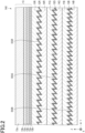
- Fig. 2 is a schematic cross-sectional view illustrating a blank medium which can be used for manufacturing the display illustrated in Fig. 1 .
- Fig. 3 is a cross-sectional view explaining a method for manufacturing the display illustrated in Fig. 1 .
- the reference sign OL indicates an objective lens of a laser device.
- the blank medium 1A0 illustrated in Fig. 2 is prepared.
- the blank medium 1A0 has the same structure as that of the display 1A except that the first recess RR, the second recess RG, and the third recess RB are not formed in the laminate.
- an image is recorded by irradiating a laminate with a laser beam.
- a laser beam LB is applied to a region of the front surface of the laminate where the first recess RR, the second recess RG, and the third recess RB are to be formed.
- the first recess RR, the second recess RG, and the third recess RB are formed on the front surface of the laminate.
- the diameter of the beam spot is typically several tens of micrometers. Therefore, the laser beam irradiation forms recesses having an opening diameter of, for example, several tens of micrometers or more.
- the depth of the recess formed by the irradiation of the laser beam LB can be adjusted, for example, by changing the number of irradiation times of the pulsed light, when a laser device is a pulsed laser. In this way, the display 1A is obtained.
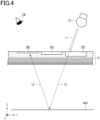
- Fig. 4 is a schematic cross-sectional view illustrating an optical behavior caused when a display according to a comparative example is illuminated with white light.
- Fig. 4 illustrates a display with a flat reflective surface REF being disposed parallel to the back surface of the multilayer film 13 and spaced apart from the back surface of the multilayer film 13, instead of disposing the first to third reflective surfaces on the back surface side of the multilayer film 13 in which the first recess RR, the second recess RG, and the third recess RB are provided.
- the display is designed as follows.
- white light L1 emitted by the light source LS is illuminated onto the front surface of the display, then at portions of the multilayer film 13 where there is no recess, none of the light components of white light incident at the first angle of incidence ⁇ 1 pass through the multilayer film 13 due to destructive interference, and thus are not reflected by the multilayer film 13.
- white light incident at the first angle of incidence ⁇ 1 light L2 having a first wavelength in the red region passes through the first portion of the multilayer film 13 aligned with the first recess RR, while light having other wavelengths does not pass through the multilayer film 13 due to destructive interference, and is not reflected by the multilayer film 13.
- white light incident at the first angle of incidence ⁇ 1 light having a second wavelength in the green region passes through the second portion of the multilayer film 13 aligned with the second recess RG, while light having other wavelengths does not pass through the multilayer film 13 due to destructive interference, and is not reflected by the multilayer film 13.
- light having a third wavelength in the blue region passes through the third portion of the multilayer film 13 aligned with the third recess RB, while light having other wavelengths does not pass through the multilayer film 13 due to destructive interference, and is not reflected by the multilayer film 13.
- the light L2 having the first wavelength in the red region passes through the first portion of the multilayer film 13 aligned with the first recess RR, while light having other wavelengths does not pass through the multilayer film 13, and is not reflected by the multilayer film 13.
- the light L2 as the transmitted light is reflected by the reflective surface REF. Since the reflective surface REF is disposed parallel to the back surface of the multilayer film 13, the light L2 as the reflected light is specularly reflected by the reflective surface REF. As a result, the light L2 enters the multilayer film 13 again at an angle of incidence equal to its angle of emergence.
- the position of the light source LS is different from the position of an observer OB. Therefore, the first angle of incidence 01 is greater than 0°, and the above-mentioned angle of emergence is also greater than 0°. Accordingly, the light L2 as the reflected light may re-enter the multilayer film 13 into a portion other than the first portion, for example, the third portion of the multilayer film 13 aligned with the third recess RB.
- the light L2 includes a first wavelength range in a red region.
- the display cannot display the intended image to the observer OB.
- Fig. 5 is a schematic cross-sectional view illustrating an optical behavior caused when the display according to Fig. 1 is illuminated with white light.
- Fig. 5 shows only a first reflective surface DG as a structure disposed on the back surface side of the multilayer film 13.
- the multilayer film 13 is designed in the same manner as described with reference to Fig. 4 .
- the light L2 having a first wavelength in the red region passes through the first portion aligned with the first recess RR, while light having other wavelengths does not pass through the multilayer film 13, and is not reflected by the multilayer film 13.
- the light L2 as the transmitted light enters the first reflective surface DG.
- the first reflective surface DG constitutes the first blazed diffraction grating.
- the first blazed diffraction grating diffracts the light L2 at the first wavelength transmitted through the first portion of the multilayer film 13 aligned with the first recess RR, and then directs the light L2 into the multilayer film 13 again at the second angle of incidence ⁇ 2 in the form of light L3.
- the transmission properties of the multilayer film 13 vary depending on the angle of incidence of the incident light.
- the second portion of the multilayer film 13 aligned with the second recess RG and the third portion of the multilayer film 13 aligned with the third recess RB do not transmit the light L2 at the first wavelength incident at the first angle of incidence ⁇ 1.
- these portions may transmit the light L3 at the first wavelength incident at the second angle of incidence ⁇ 2 which is different from the first angle of incidence ⁇ 1.
- Other portions of the multilayer film 13 might also transmit the light L3 at the first wavelength incident at the second angle of incidence ⁇ 2.
- the display can display the intended image to the observer OB.
- the display 1A described with reference to Fig. 1 is manufactured by performing laser lithography on the multilayer film 13 of the blank medium 1A0 described with reference to Fig. 2 .
- This laser lithography can be completed in a much shorter time compared to the process of transferring a hologram pixel by pixel onto a blank medium. Accordingly, the above technique achieves manufacturing a display for displaying an image by structural color in a decreased time.
- the manufacturing of the display 1A requires an advanced and complex optical design and a high degree of accuracy.
- the display 1A is thus difficult to counterfeit.
- Fig. 6 is a schematic cross-sectional view illustrating a display according to the second embodiment of the present invention.
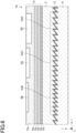
- Fig. 7 is a schematic cross-sectional view illustrating a blank medium which can be used for manufacturing the display illustrated in Fig. 6 .
- the display 1B illustrated in Fig. 6 and the blank medium 1B0 illustrated in Fig. 7 are the same as the display 1A and the blank medium 1A0 in the first embodiment, respectively, except for the points described below.
- the display 1B and the blank medium 1B0 are provided with a front layer 11, a reflective layer 12, and a back layer 14, instead of being provided with the front layers 11R, 11G, and 11B, the reflective layers 12R, 12G, and 12B, and the back layers 14R, 14G, and 14B.
- the front layer 11 is provided on the back surface of the multilayer film 13.
- the front layer 11 may be made of, for example, a transparent resin.
- the transparent resin may be a cured product of a thermosetting resin or a photocurable resin, a thermoplastic resin, an adhesive or a pressure sensitive adhesive.
- the front layer 11 may have a monolayer structure, or may have a multilayer structure.
- the back surface of the front layer 11 includes a plurality of regions, each of which is a first to third sub-region. These regions are regularly arranged on the back surface of the front layer 11. According to one example, each of these regions has a shape extending in the X direction and is arranged in the Y direction.
- the first to third sub-regions are each provided with the first to third relief structures described in the first embodiment.
- the first to third sub-regions each have a shape extending in the X direction and are arranged in the Y direction.
- the first, second, and third relief structures form a first diffraction grating DGR, a second diffraction grating DGG, and a third diffraction grating DGB, respectively, on a reflective surface, which is an interface between the front layer 11 and the reflective layer 12.
- the first recess RR, the second recess RG, and the third recess RB are each provided at the first diffraction grating DGR, the second diffraction grating DGG, and the third diffraction grating DGB, respectively.
- the reflective layer 12 covers the back surface of the front layer 11.
- the materials exemplified for the reflective layer 12B may be used.
- the back layer 14 covers the back surface of the reflective layer 12.
- the back layer 14 may be made of, for example, a transparent resin.
- the back layer 14 may be opaque.
- the resin constituting the back layer 14 may be a cured product of a thermosetting resin or a photocurable resin, a thermoplastic resin, an adhesive or a pressure sensitive adhesive.
- One or two of the front layer 11, the reflective layer 12 and the back layer 14 may be omitted. However, when only the reflective layer 12 is omitted from these, materials having refractive indices different from each other are used for the front layer 11 and the back layer 14.
- the display 1B is manufactured by the same method as described above for the display 1A except that the first recess RR, the second recess RG, and the third recess RB are formed at the positions where the first diffraction grating DGR, the second diffraction grating DGG, and the third diffraction grating DGB are disposed, respectively.
- the second embodiment effects similar to those of the first embodiment are obtained.
- metal as the material of the reflective layer 12 enables the display 1B in the second embodiment to display an image that is brighter than the display 1A in the first embodiment. Further, the display 1B in the second embodiment is easily formed thinner than the display 1A according to the first embodiment.
- FIG. 8 is a schematic cross-sectional view illustrating a display-equipped article, according to an embodiment of the present invention.
- a display-equipped article 100AB may be, for example, a printed matter.
- the display-equipped article 100AB may be, for example, bank notes, securities, certificates, credit cards, personal authentication media, such as passports or ID (identification) cards, or packages with contents contained therein.
- the display-equipped article 100AB includes a display 1AB and an article 110 retaining the display 1AB.
- the article 110 when it is a printed matter, includes a print substrate and a print layer provided thereon.
- the material of the print substrate may be, for example, plastic, metal, paper, or a composite thereof.
- the display 1AB is the display 1A or 1B described above.
- the display 1AB is retained by the article 110 so that the front surface of the display 1AB is adjacent to the outer portion of the display-equipped article 100AB.
- the display 1AB may be retained by the article 110, for example, by attaching the display 1AB to the front surface of the article 110 or embedding the display 1AB in the article 110.
- the display-equipped article 100AB can be manufactured, for example, by manufacturing the display 1AB in advance and then retaining the display 1AB on the article 110.
- the display-equipped article 100AB can be manufactured by the following method.
- Fig. 9 is a schematic cross-sectional view illustrating a blank medium-equipped article according to an embodiment of the present invention.
- the blank medium-equipped article 100AB0 shown in Fig. 9 has the same structure as that of the display-equipped article 100AB except that there are none of the first recess RR, the second recess RG, and the third recess RB are formed in the multilayer film 13.
- the blank medium-equipped article 100AB0 includes a blank-medium 1AB0 and the article 110 retaining the blank-medium 1AB0.
- the blank medium 1AB0 is the blank medium 1A0 or 1B0 described above.
- the blank medium-equipped article 100AB0 may be prepared in advance, and the display-equipped article 100AB may be manufactured by irradiating the blank medium 1AB0 with a laser beam.
- a protective layer made of a transparent material is preferably provided on the front surface of the laminate.
- the protective layer may cover only the front surface of the laminate, or may cover the front surface of the display 1AB and the front surface of the article 110.
- a thick protective layer does not affect interference in the multilayer film 13
- a thin protective layer may affect interference in the multilayer film 13.
- the protective film is used as a part of the multilayer film 13. Therefore, in this case, the multilayer film 13 is designed to exhibit the optical properties described above in a state in which the protective layer is included.
- a display having a structure similar to that of the display 1A described with reference to Fig. 1 was manufactured.
- the multilayer film 13 was composed of one dielectric layer 13a and one dielectric layer 13b.
- the dielectric layer 13a was made of a material having a refractive index of 1.98 and a thickness of 700 nm.
- the dielectric layer 13b was made of a material having a refractive index of 1.28 and a thickness of 650 nm.
- a first recess RR was formed so that the thickness of a first portion was 600 nm.
- a second recess RG was formed so that the thickness of a second portion was 300 nm.
- a third recess RB was formed so that the thickness of a third portion was 200 nm.
- the dielectric layer 13a had a protective layer formed thereon.
- a material having a refractive index of 2.5 was used as the material of the protective layer, and its thickness was sufficiently large so as not to affect interference in the multilayer film 13.
- a first blazed diffraction grating was formed so that the spatial frequency of the grating line was 1150 lines/mm.
- a second blazed diffraction grating was formed so that the spatial frequency of the grating line was 1320 lines/mm.
- a third blazed diffraction grating was formed so that the spatial frequency of the grating line was 1550 lines/mm.
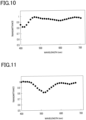
- Fig. 10 is a graph showing a transmission spectrum of the third portion of the multilayer film 13 aligned with the third recess RB, obtained by computer simulation.
- Fig. 11 is a graph showing a transmission spectrum of the third portion of the multilayer film 13 aligned with the second recess RG, obtained by computer simulation.
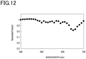
- Fig. 12 is a graph showing a transmission spectrum of the third portion of the multilayer film 13 aligned with the first recess RR, obtained by computer simulation.
- the transmittance of the portion of the multilayer film 13 having no recesses is substantially constant over the entire visible range.
- the transmittance of the blue region is lower than that of other wavelength ranges in the visible range. Therefore, the light transmitted through the third portion has a low intensity in the blue region and a high intensity in the green and red regions. Therefore, the light transmitted through the third portion appears yellow.
- the transmittance of the green region is lower than that of other wavelength ranges in the visible range. Therefore, the light transmitted through the second portion has a low intensity in the green region and a high intensity in the blue and red regions. Therefore, the light transmitted through the second portion appears magenta.
- the transmittance of the red region is lower than that of other wavelength ranges in the visible range.
- the light transmitted through the first portion has a low intensity in the red region and a high intensity in the blue and green regions. Therefore, the light transmitted through the first portion appears cyan.
- the first, second, and third blazed diffraction gratings emit strong red, green, and blue first-order diffracted light in the same direction inclined to the normal direction when illuminated with white light from the normal direction, respectively.
- the combination of the first, second, and third blazed diffraction gratings has a substantially uniform reflectance over substantially the entire visible range, and functions as a reflective surface which reflects incident light at an angle of reflection different from the angle of incidence thereof.
- this display should be able to display a color image, as a diffracted image, having a pattern corresponding to the arrangement of the first recess RR, second recess RG, and third recess RB.
- blazed diffraction gratings are used in the above embodiments, the present invention is not limited to blazed diffraction gratings, but holographic diffraction gratings and laminar diffraction gratings may also be used.
Landscapes
- Physics & Mathematics (AREA)
- Optics & Photonics (AREA)
- General Physics & Mathematics (AREA)
- Engineering & Computer Science (AREA)
- Manufacturing & Machinery (AREA)
- Health & Medical Sciences (AREA)
- Electromagnetism (AREA)
- General Health & Medical Sciences (AREA)
- Toxicology (AREA)
- Ceramic Engineering (AREA)
- Diffracting Gratings Or Hologram Optical Elements (AREA)
- Credit Cards Or The Like (AREA)
- Optical Filters (AREA)
Applications Claiming Priority (2)
| Application Number | Priority Date | Filing Date | Title |
|---|---|---|---|
| JP2019064029 | 2019-03-28 | ||
| PCT/JP2020/006493 WO2020195367A1 (ja) | 2019-03-28 | 2020-02-19 | 表示体 |
Publications (3)
| Publication Number | Publication Date |
|---|---|
| EP3951448A1 EP3951448A1 (en) | 2022-02-09 |
| EP3951448A4 EP3951448A4 (en) | 2022-06-08 |
| EP3951448B1 true EP3951448B1 (en) | 2024-10-16 |
Family
ID=72609492
Family Applications (1)
| Application Number | Title | Priority Date | Filing Date |
|---|---|---|---|
| EP20777415.9A Active EP3951448B1 (en) | 2019-03-28 | 2020-02-19 | Display body |
Country Status (5)
| Country | Link |
|---|---|
| US (1) | US12158598B2 (enExample) |
| EP (1) | EP3951448B1 (enExample) |
| JP (1) | JPWO2020195367A1 (enExample) |
| CN (1) | CN113646671B (enExample) |
| WO (1) | WO2020195367A1 (enExample) |
Families Citing this family (1)
| Publication number | Priority date | Publication date | Assignee | Title |
|---|---|---|---|---|
| JP7494591B2 (ja) * | 2020-06-16 | 2024-06-04 | Toppanホールディングス株式会社 | 表示体 |
Family Cites Families (23)
| Publication number | Priority date | Publication date | Assignee | Title |
|---|---|---|---|---|
| EP1252027A1 (en) * | 2000-01-21 | 2002-10-30 | Flex Products, Inc. | Optically variable security devices |
| KR100622868B1 (ko) * | 2003-07-29 | 2006-09-18 | 김철하 | 다층 칼라 필름 |
| EP2115501A4 (en) * | 2007-02-14 | 2012-02-01 | Aztec Systems Inc | REFLECTIVE DIFFRACTION STRUCTURE WITH SURFACE RELIEF VOLUME |
| KR101126938B1 (ko) * | 2007-05-25 | 2012-03-20 | 도판 인사츠 가부시키가이샤 | 표시체 및 정보 인쇄물 |
| JP2009134094A (ja) * | 2007-11-30 | 2009-06-18 | Toppan Printing Co Ltd | 回折構造転写箔及びそれを用いた偽造防止媒体 |
| JP2009134093A (ja) * | 2007-11-30 | 2009-06-18 | Toppan Printing Co Ltd | 回折構造物及びそれを用いた偽造防止媒体、並びに偽造防止用紙 |
| JP5315793B2 (ja) * | 2008-05-27 | 2013-10-16 | 凸版印刷株式会社 | セキュリティデバイス及びラベル付き物品 |
| JP2010173220A (ja) * | 2009-01-30 | 2010-08-12 | Toppan Printing Co Ltd | 偽造防止媒体 |
| WO2011065160A1 (ja) * | 2009-11-27 | 2011-06-03 | 凸版印刷株式会社 | 表示体及び表示体付き物品 |
| EP2508922B2 (en) * | 2009-12-01 | 2023-08-16 | Toppan Printing Co., Ltd. | Display body and labeled article |
| JP2011133677A (ja) * | 2009-12-24 | 2011-07-07 | Toppan Printing Co Ltd | ブランク媒体、画像表示体及び情報媒体 |
| WO2013084960A1 (ja) * | 2011-12-07 | 2013-06-13 | 凸版印刷株式会社 | 表示体、転写箔、及び表示体付き物品 |
| US20130330486A1 (en) * | 2012-06-07 | 2013-12-12 | Mind Flow Llc | One-Way Graphics Materials and Methods |
| JP6146632B2 (ja) | 2012-07-06 | 2017-06-14 | 大日本印刷株式会社 | 個人情報表示体の製造方法および製造装置 |
| JP6146630B2 (ja) | 2012-07-02 | 2017-06-14 | 大日本印刷株式会社 | 個人情報表示体 |
| JP6171291B2 (ja) * | 2012-09-07 | 2017-08-02 | 凸版印刷株式会社 | 表示体の真偽判定方法 |
| JP6364754B2 (ja) * | 2013-11-26 | 2018-08-01 | 凸版印刷株式会社 | 表示体、および表示体の製造方法 |
| JP6539977B2 (ja) * | 2014-10-10 | 2019-07-10 | 凸版印刷株式会社 | 表示体および表示体付き物品、ならびにそれらの真贋判定方法 |
| JP6500386B2 (ja) * | 2014-10-21 | 2019-04-17 | 凸版印刷株式会社 | 表示体、並びにこれを備えた転写箔及び物品 |
| WO2017057723A1 (ja) * | 2015-10-02 | 2017-04-06 | 凸版印刷株式会社 | 偽造防止構造体 |
| JP6874275B2 (ja) * | 2016-04-04 | 2021-05-19 | 凸版印刷株式会社 | 情報表示媒体及び情報表示媒体付き物品 |
| WO2019004229A1 (ja) * | 2017-06-28 | 2019-01-03 | 凸版印刷株式会社 | 発色構造体、表示体、発色構造体の製造方法 |
| US20190059340A1 (en) * | 2017-08-31 | 2019-02-28 | Joshua Douglas Brown | Edge-Lit Laminated Aquarium Wall and Filtration Assembly |
-
2020
- 2020-02-19 EP EP20777415.9A patent/EP3951448B1/en active Active
- 2020-02-19 CN CN202080025680.6A patent/CN113646671B/zh active Active
- 2020-02-19 JP JP2021508269A patent/JPWO2020195367A1/ja active Pending
- 2020-02-19 WO PCT/JP2020/006493 patent/WO2020195367A1/ja not_active Ceased
-
2021
- 2021-09-24 US US17/484,232 patent/US12158598B2/en active Active
Also Published As
| Publication number | Publication date |
|---|---|
| EP3951448A4 (en) | 2022-06-08 |
| CN113646671A (zh) | 2021-11-12 |
| WO2020195367A1 (ja) | 2020-10-01 |
| CN113646671B (zh) | 2023-12-22 |
| US12158598B2 (en) | 2024-12-03 |
| JPWO2020195367A1 (enExample) | 2020-10-01 |
| US20220011481A1 (en) | 2022-01-13 |
| EP3951448A1 (en) | 2022-02-09 |
Similar Documents
| Publication | Publication Date | Title |
|---|---|---|
| JP4961944B2 (ja) | 表示体及び印刷物 | |
| US9789726B2 (en) | Optically variable areal pattern | |
| RU2230671C2 (ru) | Декоративная пленка | |
| JP5741125B2 (ja) | 表示体及びラベル付き物品 | |
| KR102219805B1 (ko) | 표시체 | |
| JP5338177B2 (ja) | 表示体及びラベル付き物品 | |
| JP5338193B2 (ja) | 表示体、粘着ラベル、転写箔及びラベル付き物品 | |
| CN115066338B (zh) | 光学可变的防伪元件 | |
| JP2008275740A (ja) | 表示体及び積層体 | |
| JP5266770B2 (ja) | レリーフ構造形成層からなる表示体及びラベル付き物品 | |
| CN108466504B (zh) | 光学防伪元件和光学防伪产品 | |
| JP5515244B2 (ja) | 表示体及びラベル付き物品 | |
| JP2011002491A (ja) | 表示体及びラベル付き物品 | |
| JP6349834B2 (ja) | 表示体、表示体の製造方法、ラベル付き物品 | |
| CN108790469B (zh) | 光学防伪元件与防伪产品 | |
| JP2012123102A (ja) | 表示体及びラベル付き物品 | |
| JP5481953B2 (ja) | 表示体及びラベル付き物品 | |
| JP5272438B2 (ja) | 表示体及びラベル付き物品 | |
| JP5082378B2 (ja) | 表示体及び印刷物 | |
| EP3951448B1 (en) | Display body | |
| JP5349772B2 (ja) | 表示体及びラベル付き物品 | |
| JP2016080848A (ja) | 表示体及び表示体付き物品 | |
| JP2015024650A (ja) | 画像表示体および情報媒体 | |
| JP7494591B2 (ja) | 表示体 | |
| CN116075435B (zh) | 光学可变的防伪元件 |
Legal Events
| Date | Code | Title | Description |
|---|---|---|---|
| STAA | Information on the status of an ep patent application or granted ep patent |
Free format text: STATUS: THE INTERNATIONAL PUBLICATION HAS BEEN MADE |
|
| PUAI | Public reference made under article 153(3) epc to a published international application that has entered the european phase |
Free format text: ORIGINAL CODE: 0009012 |
|
| STAA | Information on the status of an ep patent application or granted ep patent |
Free format text: STATUS: REQUEST FOR EXAMINATION WAS MADE |
|
| 17P | Request for examination filed |
Effective date: 20210827 |
|
| AK | Designated contracting states |
Kind code of ref document: A1 Designated state(s): AL AT BE BG CH CY CZ DE DK EE ES FI FR GB GR HR HU IE IS IT LI LT LU LV MC MK MT NL NO PL PT RO RS SE SI SK SM TR |
|
| A4 | Supplementary search report drawn up and despatched |
Effective date: 20220506 |
|
| RIC1 | Information provided on ipc code assigned before grant |
Ipc: G02B 5/28 20060101ALI20220429BHEP Ipc: B32B 7/023 20190101ALI20220429BHEP Ipc: B42D 25/435 20140101ALI20220429BHEP Ipc: B42D 25/328 20140101ALI20220429BHEP Ipc: G02B 5/18 20060101AFI20220429BHEP |
|
| DAV | Request for validation of the european patent (deleted) | ||
| DAX | Request for extension of the european patent (deleted) | ||
| GRAP | Despatch of communication of intention to grant a patent |
Free format text: ORIGINAL CODE: EPIDOSNIGR1 |
|
| STAA | Information on the status of an ep patent application or granted ep patent |
Free format text: STATUS: GRANT OF PATENT IS INTENDED |
|
| INTG | Intention to grant announced |
Effective date: 20240528 |
|
| GRAS | Grant fee paid |
Free format text: ORIGINAL CODE: EPIDOSNIGR3 |
|
| GRAA | (expected) grant |
Free format text: ORIGINAL CODE: 0009210 |
|
| STAA | Information on the status of an ep patent application or granted ep patent |
Free format text: STATUS: THE PATENT HAS BEEN GRANTED |
|
| AK | Designated contracting states |
Kind code of ref document: B1 Designated state(s): AL AT BE BG CH CY CZ DE DK EE ES FI FR GB GR HR HU IE IS IT LI LT LU LV MC MK MT NL NO PL PT RO RS SE SI SK SM TR |
|
| REG | Reference to a national code |
Ref country code: GB Ref legal event code: FG4D |
|
| REG | Reference to a national code |
Ref country code: DE Ref legal event code: R096 Ref document number: 602020039603 Country of ref document: DE Ref country code: CH Ref legal event code: EP |
|
| REG | Reference to a national code |
Ref country code: IE Ref legal event code: FG4D |
|
| PGFP | Annual fee paid to national office [announced via postgrant information from national office to epo] |
Ref country code: FR Payment date: 20241231 Year of fee payment: 6 |
|
| REG | Reference to a national code |
Ref country code: LT Ref legal event code: MG9D |
|
| REG | Reference to a national code |
Ref country code: NL Ref legal event code: MP Effective date: 20241016 |
|
| REG | Reference to a national code |
Ref country code: AT Ref legal event code: MK05 Ref document number: 1733356 Country of ref document: AT Kind code of ref document: T Effective date: 20241016 |
|
| PG25 | Lapsed in a contracting state [announced via postgrant information from national office to epo] |
Ref country code: NL Free format text: LAPSE BECAUSE OF FAILURE TO SUBMIT A TRANSLATION OF THE DESCRIPTION OR TO PAY THE FEE WITHIN THE PRESCRIBED TIME-LIMIT Effective date: 20241016 |
|
| PG25 | Lapsed in a contracting state [announced via postgrant information from national office to epo] |
Ref country code: NL Free format text: LAPSE BECAUSE OF FAILURE TO SUBMIT A TRANSLATION OF THE DESCRIPTION OR TO PAY THE FEE WITHIN THE PRESCRIBED TIME-LIMIT Effective date: 20241016 |
|
| PG25 | Lapsed in a contracting state [announced via postgrant information from national office to epo] |
Ref country code: PT Free format text: LAPSE BECAUSE OF FAILURE TO SUBMIT A TRANSLATION OF THE DESCRIPTION OR TO PAY THE FEE WITHIN THE PRESCRIBED TIME-LIMIT Effective date: 20250217 Ref country code: HR Free format text: LAPSE BECAUSE OF FAILURE TO SUBMIT A TRANSLATION OF THE DESCRIPTION OR TO PAY THE FEE WITHIN THE PRESCRIBED TIME-LIMIT Effective date: 20241016 Ref country code: IS Free format text: LAPSE BECAUSE OF FAILURE TO SUBMIT A TRANSLATION OF THE DESCRIPTION OR TO PAY THE FEE WITHIN THE PRESCRIBED TIME-LIMIT Effective date: 20250216 |
|
| PGFP | Annual fee paid to national office [announced via postgrant information from national office to epo] |
Ref country code: DE Payment date: 20241231 Year of fee payment: 6 |
|
| PG25 | Lapsed in a contracting state [announced via postgrant information from national office to epo] |
Ref country code: FI Free format text: LAPSE BECAUSE OF FAILURE TO SUBMIT A TRANSLATION OF THE DESCRIPTION OR TO PAY THE FEE WITHIN THE PRESCRIBED TIME-LIMIT Effective date: 20241016 |
|
| PG25 | Lapsed in a contracting state [announced via postgrant information from national office to epo] |
Ref country code: BG Free format text: LAPSE BECAUSE OF FAILURE TO SUBMIT A TRANSLATION OF THE DESCRIPTION OR TO PAY THE FEE WITHIN THE PRESCRIBED TIME-LIMIT Effective date: 20241016 |
|
| PG25 | Lapsed in a contracting state [announced via postgrant information from national office to epo] |
Ref country code: ES Free format text: LAPSE BECAUSE OF FAILURE TO SUBMIT A TRANSLATION OF THE DESCRIPTION OR TO PAY THE FEE WITHIN THE PRESCRIBED TIME-LIMIT Effective date: 20241016 |
|
| PG25 | Lapsed in a contracting state [announced via postgrant information from national office to epo] |
Ref country code: NO Free format text: LAPSE BECAUSE OF FAILURE TO SUBMIT A TRANSLATION OF THE DESCRIPTION OR TO PAY THE FEE WITHIN THE PRESCRIBED TIME-LIMIT Effective date: 20250116 |
|
| PG25 | Lapsed in a contracting state [announced via postgrant information from national office to epo] |
Ref country code: LV Free format text: LAPSE BECAUSE OF FAILURE TO SUBMIT A TRANSLATION OF THE DESCRIPTION OR TO PAY THE FEE WITHIN THE PRESCRIBED TIME-LIMIT Effective date: 20241016 Ref country code: AT Free format text: LAPSE BECAUSE OF FAILURE TO SUBMIT A TRANSLATION OF THE DESCRIPTION OR TO PAY THE FEE WITHIN THE PRESCRIBED TIME-LIMIT Effective date: 20241016 Ref country code: GR Free format text: LAPSE BECAUSE OF FAILURE TO SUBMIT A TRANSLATION OF THE DESCRIPTION OR TO PAY THE FEE WITHIN THE PRESCRIBED TIME-LIMIT Effective date: 20250117 |
|
| PG25 | Lapsed in a contracting state [announced via postgrant information from national office to epo] |
Ref country code: PL Free format text: LAPSE BECAUSE OF FAILURE TO SUBMIT A TRANSLATION OF THE DESCRIPTION OR TO PAY THE FEE WITHIN THE PRESCRIBED TIME-LIMIT Effective date: 20241016 |
|
| PG25 | Lapsed in a contracting state [announced via postgrant information from national office to epo] |
Ref country code: RS Free format text: LAPSE BECAUSE OF FAILURE TO SUBMIT A TRANSLATION OF THE DESCRIPTION OR TO PAY THE FEE WITHIN THE PRESCRIBED TIME-LIMIT Effective date: 20250116 |
|
| PG25 | Lapsed in a contracting state [announced via postgrant information from national office to epo] |
Ref country code: SM Free format text: LAPSE BECAUSE OF FAILURE TO SUBMIT A TRANSLATION OF THE DESCRIPTION OR TO PAY THE FEE WITHIN THE PRESCRIBED TIME-LIMIT Effective date: 20241016 |
|
| PG25 | Lapsed in a contracting state [announced via postgrant information from national office to epo] |
Ref country code: DK Free format text: LAPSE BECAUSE OF FAILURE TO SUBMIT A TRANSLATION OF THE DESCRIPTION OR TO PAY THE FEE WITHIN THE PRESCRIBED TIME-LIMIT Effective date: 20241016 |
|
| REG | Reference to a national code |
Ref country code: DE Ref legal event code: R097 Ref document number: 602020039603 Country of ref document: DE |
|
| PG25 | Lapsed in a contracting state [announced via postgrant information from national office to epo] |
Ref country code: EE Free format text: LAPSE BECAUSE OF FAILURE TO SUBMIT A TRANSLATION OF THE DESCRIPTION OR TO PAY THE FEE WITHIN THE PRESCRIBED TIME-LIMIT Effective date: 20241016 |
|
| PG25 | Lapsed in a contracting state [announced via postgrant information from national office to epo] |
Ref country code: RO Free format text: LAPSE BECAUSE OF FAILURE TO SUBMIT A TRANSLATION OF THE DESCRIPTION OR TO PAY THE FEE WITHIN THE PRESCRIBED TIME-LIMIT Effective date: 20241016 |
|
| PG25 | Lapsed in a contracting state [announced via postgrant information from national office to epo] |
Ref country code: SK Free format text: LAPSE BECAUSE OF FAILURE TO SUBMIT A TRANSLATION OF THE DESCRIPTION OR TO PAY THE FEE WITHIN THE PRESCRIBED TIME-LIMIT Effective date: 20241016 |
|
| PG25 | Lapsed in a contracting state [announced via postgrant information from national office to epo] |
Ref country code: CZ Free format text: LAPSE BECAUSE OF FAILURE TO SUBMIT A TRANSLATION OF THE DESCRIPTION OR TO PAY THE FEE WITHIN THE PRESCRIBED TIME-LIMIT Effective date: 20241016 |
|
| PG25 | Lapsed in a contracting state [announced via postgrant information from national office to epo] |
Ref country code: IT Free format text: LAPSE BECAUSE OF FAILURE TO SUBMIT A TRANSLATION OF THE DESCRIPTION OR TO PAY THE FEE WITHIN THE PRESCRIBED TIME-LIMIT Effective date: 20241016 |
|
| PLBE | No opposition filed within time limit |
Free format text: ORIGINAL CODE: 0009261 |
|
| STAA | Information on the status of an ep patent application or granted ep patent |
Free format text: STATUS: NO OPPOSITION FILED WITHIN TIME LIMIT |
|
| PG25 | Lapsed in a contracting state [announced via postgrant information from national office to epo] |
Ref country code: SE Free format text: LAPSE BECAUSE OF FAILURE TO SUBMIT A TRANSLATION OF THE DESCRIPTION OR TO PAY THE FEE WITHIN THE PRESCRIBED TIME-LIMIT Effective date: 20241016 |
|
| PG25 | Lapsed in a contracting state [announced via postgrant information from national office to epo] |
Ref country code: MC Free format text: LAPSE BECAUSE OF FAILURE TO SUBMIT A TRANSLATION OF THE DESCRIPTION OR TO PAY THE FEE WITHIN THE PRESCRIBED TIME-LIMIT Effective date: 20241016 |
|
| 26N | No opposition filed |
Effective date: 20250717 |
|
| REG | Reference to a national code |
Ref country code: CH Ref legal event code: PL |
|
| PG25 | Lapsed in a contracting state [announced via postgrant information from national office to epo] |
Ref country code: LU Free format text: LAPSE BECAUSE OF NON-PAYMENT OF DUE FEES Effective date: 20250219 |
|
| PG25 | Lapsed in a contracting state [announced via postgrant information from national office to epo] |
Ref country code: CH Free format text: LAPSE BECAUSE OF NON-PAYMENT OF DUE FEES Effective date: 20250228 |
|
| GBPC | Gb: european patent ceased through non-payment of renewal fee |
Effective date: 20250219 |
|
| REG | Reference to a national code |
Ref country code: BE Ref legal event code: MM Effective date: 20250228 |