EP3936762B1 - Kompaktes kopfmontiertes anzeigesystem mit gleichförmigem bild - Google Patents
Kompaktes kopfmontiertes anzeigesystem mit gleichförmigem bild Download PDFInfo
- Publication number
- EP3936762B1 EP3936762B1 EP21193404.7A EP21193404A EP3936762B1 EP 3936762 B1 EP3936762 B1 EP 3936762B1 EP 21193404 A EP21193404 A EP 21193404A EP 3936762 B1 EP3936762 B1 EP 3936762B1
- Authority
- EP
- European Patent Office
- Prior art keywords
- waveguide
- optical system
- light
- loe
- rays
- Prior art date
- Legal status (The legal status is an assumption and is not a legal conclusion. Google has not performed a legal analysis and makes no representation as to the accuracy of the status listed.)
- Active
Links
- 239000000758 substrate Substances 0.000 claims description 54
- 230000003287 optical effect Effects 0.000 claims description 53
- 238000000576 coating method Methods 0.000 claims description 27
- 239000011248 coating agent Substances 0.000 claims description 25
- 239000010409 thin film Substances 0.000 claims description 3
- 238000009501 film coating Methods 0.000 claims description 2
- 238000000034 method Methods 0.000 description 9
- 230000000694 effects Effects 0.000 description 8
- 230000004907 flux Effects 0.000 description 5
- 238000003384 imaging method Methods 0.000 description 5
- 238000004519 manufacturing process Methods 0.000 description 5
- 239000000463 material Substances 0.000 description 4
- 101150036453 sur-2 gene Proteins 0.000 description 4
- 230000001413 cellular effect Effects 0.000 description 3
- 230000008878 coupling Effects 0.000 description 3
- 238000010168 coupling process Methods 0.000 description 3
- 238000005859 coupling reaction Methods 0.000 description 3
- 238000013461 design Methods 0.000 description 3
- 230000033001 locomotion Effects 0.000 description 3
- 230000008569 process Effects 0.000 description 3
- 210000001747 pupil Anatomy 0.000 description 3
- 238000013459 approach Methods 0.000 description 2
- 238000005286 illumination Methods 0.000 description 2
- 230000001902 propagating effect Effects 0.000 description 2
- BPQQTUXANYXVAA-UHFFFAOYSA-N Orthosilicate Chemical compound [O-][Si]([O-])([O-])[O-] BPQQTUXANYXVAA-UHFFFAOYSA-N 0.000 description 1
- 238000010521 absorption reaction Methods 0.000 description 1
- 230000008901 benefit Effects 0.000 description 1
- 230000005540 biological transmission Effects 0.000 description 1
- 239000004568 cement Substances 0.000 description 1
- 230000000295 complement effect Effects 0.000 description 1
- 230000003247 decreasing effect Effects 0.000 description 1
- 238000010586 diagram Methods 0.000 description 1
- 238000009826 distribution Methods 0.000 description 1
- 238000005516 engineering process Methods 0.000 description 1
- 230000003993 interaction Effects 0.000 description 1
- 150000002500 ions Chemical class 0.000 description 1
- 239000004973 liquid crystal related substance Substances 0.000 description 1
- 230000007246 mechanism Effects 0.000 description 1
- 238000010295 mobile communication Methods 0.000 description 1
- 239000013307 optical fiber Substances 0.000 description 1
- 238000005457 optimization Methods 0.000 description 1
- 230000010287 polarization Effects 0.000 description 1
- 229920000642 polymer Polymers 0.000 description 1
- 238000012545 processing Methods 0.000 description 1
- 230000004044 response Effects 0.000 description 1
- 210000001525 retina Anatomy 0.000 description 1
- 238000001228 spectrum Methods 0.000 description 1
- 230000009897 systematic effect Effects 0.000 description 1
- 238000002834 transmittance Methods 0.000 description 1
Images


Classifications
-
- G—PHYSICS
- G02—OPTICS
- G02B—OPTICAL ELEMENTS, SYSTEMS OR APPARATUS
- G02B27/00—Optical systems or apparatus not provided for by any of the groups G02B1/00 - G02B26/00, G02B30/00
- G02B27/01—Head-up displays
- G02B27/017—Head mounted
- G02B27/0172—Head mounted characterised by optical features
-
- G—PHYSICS
- G02—OPTICS
- G02B—OPTICAL ELEMENTS, SYSTEMS OR APPARATUS
- G02B27/00—Optical systems or apparatus not provided for by any of the groups G02B1/00 - G02B26/00, G02B30/00
- G02B27/02—Viewing or reading apparatus
- G02B27/04—Viewing or reading apparatus having collapsible parts
-
- G—PHYSICS
- G02—OPTICS
- G02B—OPTICAL ELEMENTS, SYSTEMS OR APPARATUS
- G02B27/00—Optical systems or apparatus not provided for by any of the groups G02B1/00 - G02B26/00, G02B30/00
- G02B27/0081—Optical systems or apparatus not provided for by any of the groups G02B1/00 - G02B26/00, G02B30/00 with means for altering, e.g. enlarging, the entrance or exit pupil
-
- G—PHYSICS
- G02—OPTICS
- G02B—OPTICAL ELEMENTS, SYSTEMS OR APPARATUS
- G02B27/00—Optical systems or apparatus not provided for by any of the groups G02B1/00 - G02B26/00, G02B30/00
- G02B27/01—Head-up displays
- G02B27/017—Head mounted
- G02B27/0176—Head mounted characterised by mechanical features
-
- G—PHYSICS
- G02—OPTICS
- G02B—OPTICAL ELEMENTS, SYSTEMS OR APPARATUS
- G02B27/00—Optical systems or apparatus not provided for by any of the groups G02B1/00 - G02B26/00, G02B30/00
- G02B27/10—Beam splitting or combining systems
- G02B27/14—Beam splitting or combining systems operating by reflection only
- G02B27/142—Coating structures, e.g. thin films multilayers
-
- G—PHYSICS
- G02—OPTICS
- G02B—OPTICAL ELEMENTS, SYSTEMS OR APPARATUS
- G02B27/00—Optical systems or apparatus not provided for by any of the groups G02B1/00 - G02B26/00, G02B30/00
- G02B27/10—Beam splitting or combining systems
- G02B27/14—Beam splitting or combining systems operating by reflection only
- G02B27/145—Beam splitting or combining systems operating by reflection only having sequential partially reflecting surfaces
-
- G—PHYSICS
- G02—OPTICS
- G02B—OPTICAL ELEMENTS, SYSTEMS OR APPARATUS
- G02B27/00—Optical systems or apparatus not provided for by any of the groups G02B1/00 - G02B26/00, G02B30/00
- G02B27/10—Beam splitting or combining systems
- G02B27/14—Beam splitting or combining systems operating by reflection only
- G02B27/148—Beam splitting or combining systems operating by reflection only including stacked surfaces having at least one double-pass partially reflecting surface
-
- G—PHYSICS
- G02—OPTICS
- G02B—OPTICAL ELEMENTS, SYSTEMS OR APPARATUS
- G02B27/00—Optical systems or apparatus not provided for by any of the groups G02B1/00 - G02B26/00, G02B30/00
- G02B27/28—Optical systems or apparatus not provided for by any of the groups G02B1/00 - G02B26/00, G02B30/00 for polarising
- G02B27/283—Optical systems or apparatus not provided for by any of the groups G02B1/00 - G02B26/00, G02B30/00 for polarising used for beam splitting or combining
-
- G—PHYSICS
- G02—OPTICS
- G02B—OPTICAL ELEMENTS, SYSTEMS OR APPARATUS
- G02B6/00—Light guides; Structural details of arrangements comprising light guides and other optical elements, e.g. couplings
-
- G—PHYSICS
- G02—OPTICS
- G02B—OPTICAL ELEMENTS, SYSTEMS OR APPARATUS
- G02B6/00—Light guides; Structural details of arrangements comprising light guides and other optical elements, e.g. couplings
- G02B6/0001—Light guides; Structural details of arrangements comprising light guides and other optical elements, e.g. couplings specially adapted for lighting devices or systems
- G02B6/0011—Light guides; Structural details of arrangements comprising light guides and other optical elements, e.g. couplings specially adapted for lighting devices or systems the light guides being planar or of plate-like form
- G02B6/0013—Means for improving the coupling-in of light from the light source into the light guide
- G02B6/0015—Means for improving the coupling-in of light from the light source into the light guide provided on the surface of the light guide or in the bulk of it
- G02B6/0016—Grooves, prisms, gratings, scattering particles or rough surfaces
-
- G—PHYSICS
- G02—OPTICS
- G02B—OPTICAL ELEMENTS, SYSTEMS OR APPARATUS
- G02B6/00—Light guides; Structural details of arrangements comprising light guides and other optical elements, e.g. couplings
- G02B6/0001—Light guides; Structural details of arrangements comprising light guides and other optical elements, e.g. couplings specially adapted for lighting devices or systems
- G02B6/0011—Light guides; Structural details of arrangements comprising light guides and other optical elements, e.g. couplings specially adapted for lighting devices or systems the light guides being planar or of plate-like form
- G02B6/0033—Means for improving the coupling-out of light from the light guide
- G02B6/0035—Means for improving the coupling-out of light from the light guide provided on the surface of the light guide or in the bulk of it
-
- G—PHYSICS
- G02—OPTICS
- G02B—OPTICAL ELEMENTS, SYSTEMS OR APPARATUS
- G02B6/00—Light guides; Structural details of arrangements comprising light guides and other optical elements, e.g. couplings
- G02B6/0001—Light guides; Structural details of arrangements comprising light guides and other optical elements, e.g. couplings specially adapted for lighting devices or systems
- G02B6/0011—Light guides; Structural details of arrangements comprising light guides and other optical elements, e.g. couplings specially adapted for lighting devices or systems the light guides being planar or of plate-like form
- G02B6/0033—Means for improving the coupling-out of light from the light guide
- G02B6/005—Means for improving the coupling-out of light from the light guide provided by one optical element, or plurality thereof, placed on the light output side of the light guide
- G02B6/0055—Reflecting element, sheet or layer
-
- G—PHYSICS
- G02—OPTICS
- G02B—OPTICAL ELEMENTS, SYSTEMS OR APPARATUS
- G02B27/00—Optical systems or apparatus not provided for by any of the groups G02B1/00 - G02B26/00, G02B30/00
- G02B27/01—Head-up displays
- G02B27/0101—Head-up displays characterised by optical features
- G02B2027/0118—Head-up displays characterised by optical features comprising devices for improving the contrast of the display / brillance control visibility
- G02B2027/012—Head-up displays characterised by optical features comprising devices for improving the contrast of the display / brillance control visibility comprising devices for attenuating parasitic image effects
-
- G—PHYSICS
- G02—OPTICS
- G02B—OPTICAL ELEMENTS, SYSTEMS OR APPARATUS
- G02B27/00—Optical systems or apparatus not provided for by any of the groups G02B1/00 - G02B26/00, G02B30/00
- G02B27/01—Head-up displays
- G02B27/0101—Head-up displays characterised by optical features
- G02B2027/0123—Head-up displays characterised by optical features comprising devices increasing the field of view
- G02B2027/0125—Field-of-view increase by wavefront division
-
- G—PHYSICS
- G02—OPTICS
- G02B—OPTICAL ELEMENTS, SYSTEMS OR APPARATUS
- G02B27/00—Optical systems or apparatus not provided for by any of the groups G02B1/00 - G02B26/00, G02B30/00
- G02B27/01—Head-up displays
- G02B27/0149—Head-up displays characterised by mechanical features
- G02B2027/015—Head-up displays characterised by mechanical features involving arrangement aiming to get less bulky devices
-
- G—PHYSICS
- G02—OPTICS
- G02B—OPTICAL ELEMENTS, SYSTEMS OR APPARATUS
- G02B27/00—Optical systems or apparatus not provided for by any of the groups G02B1/00 - G02B26/00, G02B30/00
- G02B27/01—Head-up displays
- G02B27/0149—Head-up displays characterised by mechanical features
- G02B2027/0152—Head-up displays characterised by mechanical features involving arrangement aiming to get lighter or better balanced devices
-
- G—PHYSICS
- G02—OPTICS
- G02B—OPTICAL ELEMENTS, SYSTEMS OR APPARATUS
- G02B27/00—Optical systems or apparatus not provided for by any of the groups G02B1/00 - G02B26/00, G02B30/00
- G02B27/01—Head-up displays
- G02B27/017—Head mounted
- G02B2027/0178—Eyeglass type
Definitions
- the present invention relates to substrate-guided optical devices, and particularly to devices which include a plurality of reflecting surfaces carried by a common light-transmissive substrate, also referred to as a light-guide optical element (LOE).
- a common light-transmissive substrate also referred to as a light-guide optical element (LOE).
- LOE light-guide optical element
- the invention can be implemented to advantage in a large number of imaging applications, such as, for example, head-mounted and head-up displays, cellular phones, compact displays, 3-D displays, compact beam expanders as well as non-imaging applications such as flat-panel indicators, compact illuminators and scanners.
- imaging applications such as, for example, head-mounted and head-up displays, cellular phones, compact displays, 3-D displays, compact beam expanders as well as non-imaging applications such as flat-panel indicators, compact illuminators and scanners.
- an optical module serves both as an imaging lens and a combiner, in which a two-dimensional display is imaged to infinity and reflected into the eye of an observer.
- the display can be obtained directly from either a spatial light modulator (SLM) such as a cathode ray tube (CRT), a liquid crystal display (LCD), an organic light emitting diode array (OLED), or a scanning source and similar devices, or indirectly, by means of a relay lens or an optical fiber bundle.
- SLM spatial light modulator
- CTR cathode ray tube
- LCD liquid crystal display
- OLED organic light emitting diode array
- the display comprises an array of elements (pixels) imaged to infinity by a collimating lens and transmitted into the eye of the viewer by means of a reflecting or partially reflecting surface acting as a combiner for non-see-through and see-through applications, respectively.
- a conventional, free-space optical module is used for these purposes.
- FOV field-of-view
- US2008094586 discloses image display optical systems that extend the angle of view longitudinally and transversely while saving space.
- the image display optical system includes a prism-shaped substrate transparent to an image-carrying light flux to be projected to a viewing eye, an introduction unit that guides the image-carrying light flux to a propagation path through which the image-carrying light flux propagates in a direction in which the image-carrying light flux from the outside enables internal reflection at least at three surfaces including at least one side of the substrate, and an output unit that guides the image-carrying light flux propagating through the substrate from the substrate to the viewing eye.
- the present invention facilitates the design and fabrication of very compact LOEs for, amongst other applications, head-mounted displays.
- the invention allows relatively wide FOVs together with relatively large eye-motion-box values.
- the resulting optical system offers a large, high-quality image, which also accommodates large movements of the eye.
- the optical system offered by the present invention is particularly advantageous because it is substantially more compact than state-of-the-art implementations, and yet it can be readily incorporated even into optical systems having specialized configurations.
- a further application of the present invention is to provide a compact display with a wide FOV for mobile, hand-held applications such as cellular phones.
- sufficient bandwidth is available for full video transmission.
- the limiting factor remains the quality of the display within the device of the end-user.
- the mobility requirement restricts the physical size of the displays, and the result is a direct-display with poor image viewing quality.
- the present invention enables a physically very compact display with a very large virtual image. This is a key feature in mobile communications, and especially for mobile internet access, solving one of the main limitations for its practical implementation.
- the present invention thereby enables the viewing of the digital content of a full format internet page within a small, hand-held device, such as a cellular phone.
- the broad object of the present invention is therefore to alleviate the drawbacks of state-of-the-art compact optical display devices and to provide other optical components and systems having improved performance, according to specific requirements.
- an optical device comprising a light-transmitting substrate having an input aperture, an output aperture, at least two major surfaces and edges, an optical element for coupling light waves into the substrate by total internal reflection, at least one partially reflecting surface located between the two major surfaces of the light-transmitting substrate for partially reflecting light waves out of the substrate, a first transparent plate, having at least two major surfaces, one of the major surfaces of the transparent plate being optically attached to a major surface of the light-transmitting substrate defining an interface plane, and a beam-splitting coating applied at the interface plane between the substrate and the transparent plate, wherein light waves coupled inside the light-transmitting substrate are partially reflected from the interface plane and partially pass therethrough.
- Fig. 1 illustrates a sectional view of a light-guide optical element (LOE), according to the present invention.
- the first reflecting surface 16 is illuminated by a collimated display 18 emanating from a light source (not shown) located behind the device.
- the reflecting surface 16 reflects the incident light from the source such that the light is trapped inside a planar substrate 20 by total internal reflection. After several reflections off the surfaces 26, 27 of the substrate, the trapped light waves reach an array of partially reflecting surfaces 22, which couple the light out of the substrate into the eye 24, having a pupil 25, of a viewer.
- the input surface of the LOE will be defined as the surface through which the input light waves enter the LOE and the output surface of the LOE will be defined as the surface through which the trapped light waves exit the LOE.
- the input aperture of the LOE will be referred to as the part of the input surface through which the input light waves actually pass while entering the LOE
- the output aperture of the LOE will be referred to as a part of the output surface through which the output light waves actually pass while exiting the LOE.
- both of the input and the output surfaces coincide with the lower surface 26, however, other configurations are envisioned in which the input and the image light waves could be located on opposite sides of the substrate, or on one of the edges of the LOE.
- the trapped rays arrive at the reflecting surfaces from two distinct directions 28, 30.
- each ray first arrives at the surface from the direction 30, wherein some of the rays again impinge on the surface from direction 28.
- the reflectance be negligible for the rays that impinge on the surface having the second direction 28.
- the ray then intersects the same selectively partially reflecting surface at point 84 at an incident angle of 75° without noticeable reflection, and then intersects again at point 86 at an incident angle of 25°, where another portion of the energy of the ray is coupled out of the substrate.
- the ray 88 shown in Fig. 2B experiences only one reflection 90 from the same surface. Further multiple reflections occur at other partially reflecting surfaces.
- Fig. 3 illustrates this non-uniformity phenomenon with a detailed sectional view of the partially reflective surface 22, which couples light trapped inside the substrate out and into the eye 24 of a viewer.
- the ray 80 is reflected off the upper surface 27, next to the line 100, which is the intersection of the reflecting surface 22 with the upper surface 27. Since this ray does not impinge on the reflecting surface 22, its brightness remains the same and its first incidence at surface 22 is at the point 102, after double reflection from both external surfaces. At this point, the light wave is partially reflected and the ray 104 is coupled out of the substrate 20.
- the human eye tolerates significant variations in brightness, which remain unnoticed.
- the eye integrates the light which emerges from a single viewing angle and focuses it onto one point on the retina, and since the response curve of the eye is logarithmic, small variations, if any, in the brightness of the display will not be noticeable. Therefore, even for moderate levels of illumination uniformity within the display, the human eye experiences a high-quality image.
- the required moderate uniformity can readily be achieved with the element illustrated in Fig. 1 .
- a comparatively large number of partially reflecting surfaces is required, to achieve the desired output aperture.
- the non-uniformity due to the multiple intersections with the large number of partially reflecting surfaces becomes more dominant, especially for displays located at a distance from the eye, such as head-up displays and the non-uniformity cannot be accepted.
- a more systematic method to overcome the non-uniformity is required.
- the "darker" portions of the partially reflecting surfaces 22 contribute less to the coupling of the trapped light waves out of the substrate, their impact on the optical performance of the LOE can be only be negative, namely, there will be darker portions in the output aperture of the system and dark stripes will exist in the image.
- the transparency of each one of the reflecting surfaces is, however, uniform with respect to the light waves from the external scene. Therefore, if overlapping is set between the reflective surfaces to compensate for the darker portions in the output aperture, then rays from the output scene that cross these overlapped areas will suffer from double attenuations, and darker stripes will be created in the external scene. This phenomenon significantly reduces the performance not only of displays which are located at a distance from the eye, such as head-up displays, but also that of near-eye displays, and hence, it cannot be utilized.
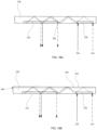
- Fig. 4 illustrates an embodiment for overcoming this problem.
- Only the “bright" portions of the partially reflecting surfaces 22a, 22b and 22c are embedded inside the substrate, namely, the reflecting surfaces 22a, 22b and 22c no longer intersect with the lower major surface 26, but terminate short of this surface. Since the ends of the reflecting surfaces are adjacent to one another over the length of the LOE, there will be no gaps in the projected image, and since there is no overlap between the surfaces there will be no gaps in the external view.
- this LOE There are several ways to construct this LOE, one of which is to attach a transparent plate 120 having a thickness T , preferably by optical cementing, to the active area of the substrate. In order to utilize only the active areas of the reflective surfaces 22 in the correct manner, it is important to calculate the actual active area of each partially reflective surface and the required thickness T of the plate 120.
- the trapped angle ⁇ in can be varied as a function of the FOV, it is important to know with which angle to associate each reflecting surface 22n, in order to calculate its active aperture.
- ⁇ sur 64°.
- Fig. 7 which is a sectional view of a compact LOE display system based on the proposed configuration, illustrates this effect.
- a single plane light wave 112 representing a particular viewing angle 114, illuminates only part of the overall array of partially reflecting surfaces 22a, 22b and 22c.
- a nominal viewing angle is defined, and the required active area of the reflecting surface is calculated according to this angle.
- the exact, detailed design of the active area of the various partially reflective surfaces is performed as follows: for each particular surface, a ray is plotted (taking refraction, due to Snell's Law, into consideration) from the left edge of the surface to the center of the designated eye pupil 25.
- the calculated direction is set as the nominal incident direction and the particular active area is calculated according to that direction.
- the exact values of the reflecting surfaces active areas can be used to determine the various distances T between the left edge 102 of the bright part of each reflecting surface 22 n and the lower surface 26.
- a larger active area dictates a smaller inter-surface distance.
- This distance represents the thickness of the plate 120 ( Fig. 7 ) that should be attached to the lower surface of the LOE.
- Fig. 8 illustrates the required thickness T of the plate 120 as a function of the field angle, for the same parameters as set above in reference to Fig. 6 . It is worthwhile setting the thickness T as the maximal calculated value to assure that the phenomenon of dark stripes will be avoided in the image. Setting a too thick plate 120 will cause an opposite effect, namely, the appearance of bright stripes in the image.
- two light rays, 122 and 124 are coupled inside the substrate 20.
- the two rays are partially reflected from surface 22a at points 126 and 128, respectively.
- the brightness of ray 124, which impinges on surface 22c at point 134 is higher than that of ray 122 at point 132. Therefore, the brightness of the coupled-out ray 138 from point 134 is higher than that of ray 136 which is coupled-out from point 132, and a bright stripe will appear in the image. Consequently, an exact value of the thickness T should be chosen to avoid dark as well as bright stripes in the image.
- a possible example not according to the invention for achieving the required structure, wherein the thickness T of the plate 120 depends on the viewing angle, is to construct a wedged substrate 20', wherein the two major surfaces are not parallel.
- a complementary transparent wedged plate 120' is attached to the substrate, preferably by optical cementing, in such a way that the combined structure forms a complete rectangular parallelepiped, i.e., the two outer major surfaces of the final LOE are parallel to each other.
- this solution is efficient for systems having small EMB, wherein there is a good matching between the viewing angle and the lateral position on the substrate plane.
- systems having a large EMB namely, wherein the eye can move significantly along the lateral axis, there will be no good adjustment between the viewing angle and the actual thickness of the plate 120'. Hence, dark or bright stripes may be seen in the image.
- This occurrence of dark or bright stripes due to the structure of the partially reflective surfaces in the LOE is not limited to the surface which creates this phenomenon.
- the brightness of the coupled ray 88 which is reflected twice by surface 22a, is lower at point 110 than that of ray 80, which is reflected only once from surface 22a at point 102.
- the brightness of the reflected wave 112 is lower than that of the adjacent ray 104.
- not only the brightness of the reflected wave from surface 22a is different, but also the brightness of the transmitted rays 140 and 142 is different.
- Another source for unevenness of the image can be the non-uniformity of the image waves which are coupled into the LOE.
- two rays 152 and 154 are located at the edges of the plane wave 156, which originates from the same point in the display source (not shown).
- the two exit rays 160 and 162 which originated from rays 152 and 154, respectively, and reflected from surface 22a, have accordingly different brightness. Unlike the input light wave 156, however, the two different rays are adjacent to each other, and this dissimilarity will easily be seen as a dark stripe in the image. These two rays 164, 165 will continue to propagate together, adjacent to each other, inside the LOE and will create a dark stripe at each place that they will be coupled out together. Naturally, the best way to avoid this unevenness is to assure that all the coupled light waves into the LOE have a uniform brightness over the entire input aperture for the entire FOV. This demand might be very difficult to fulfil for systems having large FOV as well as wide input apertures.
- this unevenness problem may be solved by attaching a transparent plate to one of the major surfaces of the LOE, as described above with reference to Fig. 4 .
- a beam splitting coating 166 is applied to the interface plane 167 between the LOE 20 and the transparent plate 120.
- two light rays, 168 and 170 are coupled inside the substrate 20. Only ray 168 impinges on the first partially reflective surface 22a at point 172 and is partially reflected there, while ray 170 skips over surface 22a, without any reflectance.
- the rays exchange energies with two other rays (not shown) at intersection points 180 and 182.
- the two reflected rays 184 and 186 from surface 22b will have substantially similar brightness and the bright stripe effect will be significantly improved.
- two light rays, 188 and 190 are coupled inside the substrate 20. Only ray 188, however, impinges on the first partially reflective surface 22a at point 192 and partially reflected there before being reflected by the upper surface 27. As a result, assuming that the two rays have the same brightness while coupled into the LOE, ray 190 which is reflected downward from the upper major surface 27, has a higher brightness then ray 188. These two rays, however, intersect each other at point 194 which is located at the interface plane 167 and exchange energies there. In addition, these two rays intersect with other rays at the points 196 and 198 which are located on the beam splitting surface 167.
- the rays 200 and 202 which are reflected from surface 22a and consequentially the rays 204 and 206 which are reflected from surface 22b, will have substantially the same brightness, and therefore, the dark stripes effect will be significantly decreased.
- This improved uniformity of brightness effect is applicable also for dark and bright stripes, which are caused by a non-uniform illumination at the input aperture of the LOE.
- the brightness distribution of the optical waves, which is trapped inside the LOE, is substantially more uniform over the output aperture of the LOE than over the input aperture.
- the light rays 184, 186 which are reflected from surface 22a, intersect with the beam splitting surface 167, before being coupled out from the LOE.
- a simple reflecting coating cannot be easily applied to surface 167 since this surface should also be transparent to the light-waves that exit the substrate 20 as well as transparent to the light wave from the external scene for see-through applications, namely, the light-waves should pass through plane 167 at small incident angles, and be partially reflected at higher incident angles.
- the passing incident angles are between 0° and 15° and the partially reflecting incident angles are between 40° and 65°.
- Fig. 14 illustrates an example not according to the invention for s-polarization the reflectance curves as functions of the incident angles for three representative wavelengths in the photopic region: 470 nm, 550 nm and 630 nm.
- For p-polarized light-waves it is impossible to achieve substantial reflectance at incident angles between 40° and 65°, due to the proximity to the Brewster angle.
- the polarization which is usually utilized for an LOE-based imaging system is the s-polarization
- the required beam splitter can be fairly easily applied.
- the beam splitting coating should be substantially transparent for light waves from the external scene which impinge on the interface surface at low incident angles and which are substantially non-polarized, the coating should have low reflectance (below 5%) at small incident angles also for p-polarized light waves.
- a difficulty still existing is that the LOE 20 is assembled from several different components. Since the fabrication process usually involves cementing optical elements, and since the required angular-sensitive reflecting coating is applied to the light-guide surface only after the body of the LOE 20 is complete, it is not possible to utilize the conventional hot-coating procedures that may damage the cemented areas. Novel thin-film technologies, as well as ion-assisted coating procedures, can also be used for cold processing. Eliminating the need to heat parts, allows cemented parts to be safely coated. An alternative is that the required coating can simply be applied to transparent plate 120, which is adjacent to the LOE 20, utilizing conventional hot-coating procedures and then cementing it at the proper place. Clearly, his alternative approach can be utilized only if the transparent plate 120 is not too thin and hence might be deformed during the coating process.
- the light waves are coupled out from the substrate by partially reflecting surfaces, which are oriented at an oblique angle in relation to the major surfaces, and usually coated with a dielectric coating.
- Fig. 18A there are systems wherein the light waves are coupled into and out from the substrate utilizing diffractive elements 230 and 232, respectively.
- diffractive elements 230 and 232 respectively.
- the same uniformity issues that were discussed above should also be relevant to this configuration.
- the two rays 234 and 236 from the same point in the display source are coupled into the substrate 238 remotely located from each other at the two edges of the coupling-in element 230.
- the rays are coupled-out by the coupling-out element 232 located adjacent to each other.
- any dissimilarity between the rays will be easily seen in the coupled-out wave.
- the diffractive efficiency of the coupling-out element 232 is increased gradually.
- different rays from the same point source might pass through different locations in the element 232 before being coupled-out the element and hence will have different brightness in the image.
- Another source for the unevenness can be caused by the fact that the ray 234 is partially diffracted out of the substrate at the right edge 240 of the grating 232 while ray 236 impinges on the lower surface just left of the grating, and hence, is not diffracted there.
- ray 236 will have a higher brightness and this difference will easily be seen.
- Fig. 18B illustrates a similar approach to solve these issues.
- a transparent plate 242 is cemented to the upper surface 244 of the substrate 238, wherein the interface surface 246 is coated with a beam-splitting coating similar to the above-described coatings.
Landscapes
- Physics & Mathematics (AREA)
- General Physics & Mathematics (AREA)
- Optics & Photonics (AREA)
- Optical Elements Other Than Lenses (AREA)
- Devices For Indicating Variable Information By Combining Individual Elements (AREA)
- Optical Couplings Of Light Guides (AREA)
- Diffracting Gratings Or Hologram Optical Elements (AREA)
- Eyeglasses (AREA)
- Mechanical Light Control Or Optical Switches (AREA)
- Planar Illumination Modules (AREA)
- Light Guides In General And Applications Therefor (AREA)
Claims (15)
- Optisches System, umfassend:einen Wellenleiter (20) mit zwei Hauptoberflächen (26, 27);eine Einkopplungseinrichtung (16, 230), wobei der Einkopplungseinrichtung (16, 230) dazu ausgebildet ist, Licht in den Wellenleiter (20) einzukoppeln, und wobei der Wellenleiter (20) dazu ausgebildet ist, Licht durch interne Totalreflexion auszubreiten;eine Auskopplungseinrichtung (22, 232), wobei der Auskopplungseinrichtung (22, 232) dazu ausgebildet ist, Licht aus dem Wellenleiter (20) auszukoppeln;und ein teilreflektierendes Element (166), das dazu ausgebildet ist, bevor das Licht aus dem Wellenleiter durch die Auskopplungseinrichtung ausgekoppelt wird, einen ersten Teil des Lichts zu übertragen und gleichzeitig einen zweiten Teil des Lichts zu reflektieren, wobei das mindestens eine teilreflektierende Element eine strahlteilende Fläche (166) ist, die innerhalb des Wellenleiters (20) zwischen und parallel zu den Hauptflächen (26, 27) des Wellenleiters integriert ist, und wobei die strahlteilende Fläche (166) als eine dielektrische Dünnfilmbeschichtung ausgebildet ist, die mit einem allmählich ansteigenden Reflexionsvermögen von 35% bei einem Einfallswinkel von 40° zu 60% bei einem Einfallswinkel von 65° für s-polarisiertes Licht mit einer Wellenlänge von 550 nm teilweise reflektierend und teilweise durchlässig ist.
- Optisches System nach Anspruch 1, ferner umfassend eine Mehrzahl von teilreflektierenden Elementen (166).
- Optisches System nach Anspruch 2, wobei der Wellenleiter eine Mehrzahl von Wellenleitersubstraten (20) umfasst.
- Optisches System nach Anspruch 1, wobei die Einkopplungseinrichtung (16, 230) und/oder die Auskopplungseinrichtung (22, 232) in den Wellenleiter (20) integriert ist.
- Optisches System nach Anspruch 4, wobei die Einkopplungseinrichtung (16, 230) und/oder die Auskopplungseinrichtung (22, 232) am Wellenleiter (20) angeordnet ist.
- Optisches System nach Anspruch 4, wobei die Einkopplungseinrichtung (16, 230) und/oder die Auskopplungseinrichtung (22, 232) innerhalb des Wellenleiters (20) integriert ist.
- Optisches System nach Anspruch 3, wobei der Wellenleiter (20) ein erstes und ein zweites Wellenleitersubstrat (20, 120) und eine Schicht (166) zwischen dem ersten und dem zweiten Wellenleitersubstrat aufweist.
- Optisches System nach Anspruch 1, wobei das teilreflektierende Element durch eine strahlteilende Beschichtung (166) gebildet ist.
- Optisches System nach Anspruch 7, wobei das teilweise reflektierende Element eine strahlteilende Beschichtung (166) auf der Oberfläche des ersten oder zweiten Wellenleitersubstrats (20, 120) umfasst.
- Optisches System nach Anspruch 1, wobei die Auskopplungseinrichtung (22, 232) einen Blendespiegel aufweist.
- Optisches System nach einem der Ansprüche 1 bis 10, wobei das teilreflektierende Element die Auskopplungseinrichtung zumindest teilweise räumlich überdeckt.
- Optisches System nach Anspruch 1, wobei die Einkopplungseinrichtung und die Auskopplungseinrichtung ein Beugungsgitter (232) umfassen.
- Optisches System nach Anspruch 1, wobei das teilweise reflektierende Element (166) ein hohes Reflexionsvermögen bei großen Einfallswinkeln und ein niedriges Reflexionsvermögen bei niedrigen Einfallswinkeln aufweist.
- Optisches System nach Anspruch 2, wobei die teilweise reflektierenden Elemente (166) ein hohes Reflexionsvermögen bei großen Einfallswinkeln und ein niedriges Reflexionsvermögen bei niedrigen Einfallswinkeln aufweisen.
- Optisches System nach Anspruch 3, wobei die teilweise reflektierenden Elemente (166) ein hohes Reflexionsvermögen bei großen Einfallswinkeln und ein niedriges Reflexionsvermögen bei niedrigen Einfallswinkeln aufweisen.
Priority Applications (1)
| Application Number | Priority Date | Filing Date | Title |
|---|---|---|---|
| EP23174554.8A EP4235238A3 (de) | 2015-02-19 | 2016-02-10 | Kompaktes kopfmontiertes anzeigesystem mit gleichförmigem bild |
Applications Claiming Priority (4)
| Application Number | Priority Date | Filing Date | Title |
|---|---|---|---|
| IL237337A IL237337B (en) | 2015-02-19 | 2015-02-19 | A compact head-up display system with a uniform image |
| PCT/IL2016/050158 WO2016132347A1 (en) | 2015-02-19 | 2016-02-10 | Compact head-mounted display system having uniform image |
| EP16710013.0A EP3259523B1 (de) | 2015-02-19 | 2016-02-10 | Kompaktes kopfmontiertes anzeigesystem mit gleichförmigem bild |
| EP19190146.1A EP3587916B1 (de) | 2015-02-19 | 2016-02-10 | Kompaktes kopfmontiertes anzeigesystem mit gleichförmigem bild |
Related Parent Applications (3)
| Application Number | Title | Priority Date | Filing Date |
|---|---|---|---|
| EP19190146.1A Division EP3587916B1 (de) | 2015-02-19 | 2016-02-10 | Kompaktes kopfmontiertes anzeigesystem mit gleichförmigem bild |
| EP19190146.1A Division-Into EP3587916B1 (de) | 2015-02-19 | 2016-02-10 | Kompaktes kopfmontiertes anzeigesystem mit gleichförmigem bild |
| EP16710013.0A Division EP3259523B1 (de) | 2015-02-19 | 2016-02-10 | Kompaktes kopfmontiertes anzeigesystem mit gleichförmigem bild |
Related Child Applications (1)
| Application Number | Title | Priority Date | Filing Date |
|---|---|---|---|
| EP23174554.8A Division EP4235238A3 (de) | 2015-02-19 | 2016-02-10 | Kompaktes kopfmontiertes anzeigesystem mit gleichförmigem bild |
Publications (2)
| Publication Number | Publication Date |
|---|---|
| EP3936762A1 EP3936762A1 (de) | 2022-01-12 |
| EP3936762B1 true EP3936762B1 (de) | 2023-05-24 |
Family
ID=55538308
Family Applications (4)
| Application Number | Title | Priority Date | Filing Date |
|---|---|---|---|
| EP19190146.1A Active EP3587916B1 (de) | 2015-02-19 | 2016-02-10 | Kompaktes kopfmontiertes anzeigesystem mit gleichförmigem bild |
| EP21193404.7A Active EP3936762B1 (de) | 2015-02-19 | 2016-02-10 | Kompaktes kopfmontiertes anzeigesystem mit gleichförmigem bild |
| EP16710013.0A Active EP3259523B1 (de) | 2015-02-19 | 2016-02-10 | Kompaktes kopfmontiertes anzeigesystem mit gleichförmigem bild |
| EP23174554.8A Pending EP4235238A3 (de) | 2015-02-19 | 2016-02-10 | Kompaktes kopfmontiertes anzeigesystem mit gleichförmigem bild |
Family Applications Before (1)
| Application Number | Title | Priority Date | Filing Date |
|---|---|---|---|
| EP19190146.1A Active EP3587916B1 (de) | 2015-02-19 | 2016-02-10 | Kompaktes kopfmontiertes anzeigesystem mit gleichförmigem bild |
Family Applications After (2)
| Application Number | Title | Priority Date | Filing Date |
|---|---|---|---|
| EP16710013.0A Active EP3259523B1 (de) | 2015-02-19 | 2016-02-10 | Kompaktes kopfmontiertes anzeigesystem mit gleichförmigem bild |
| EP23174554.8A Pending EP4235238A3 (de) | 2015-02-19 | 2016-02-10 | Kompaktes kopfmontiertes anzeigesystem mit gleichförmigem bild |
Country Status (11)
| Country | Link |
|---|---|
| US (3) | US20180039082A1 (de) |
| EP (4) | EP3587916B1 (de) |
| JP (4) | JP6585727B2 (de) |
| KR (3) | KR102642251B1 (de) |
| CN (2) | CN112198662B (de) |
| BR (1) | BR112017017773A2 (de) |
| CA (2) | CA2976604C (de) |
| IL (1) | IL237337B (de) |
| RU (1) | RU2717897C2 (de) |
| SG (1) | SG11201706330VA (de) |
| WO (1) | WO2016132347A1 (de) |
Families Citing this family (69)
| Publication number | Priority date | Publication date | Assignee | Title |
|---|---|---|---|---|
| IL166799A (en) | 2005-02-10 | 2014-09-30 | Lumus Ltd | Aluminum shale surfaces for use in a conductive substrate |
| US10073264B2 (en) | 2007-08-03 | 2018-09-11 | Lumus Ltd. | Substrate-guide optical device |
| US10048499B2 (en) | 2005-11-08 | 2018-08-14 | Lumus Ltd. | Polarizing optical system |
| IL232197B (en) | 2014-04-23 | 2018-04-30 | Lumus Ltd | Compact head-up display system |
| IL235642B (en) | 2014-11-11 | 2021-08-31 | Lumus Ltd | A compact head-up display system is protected by an element with a super-thin structure |
| IL237337B (en) * | 2015-02-19 | 2020-03-31 | Amitai Yaakov | A compact head-up display system with a uniform image |
| US11016306B2 (en) * | 2015-09-02 | 2021-05-25 | Sony Corporation | Optical device and method for producing the same, and display device |
| EP3407116A4 (de) * | 2016-01-18 | 2019-09-25 | Shimadzu Corporation | Optisches element, anzeigevorrichtung damit und lichtempfangende vorrichtung |
| US9964769B2 (en) | 2016-06-10 | 2018-05-08 | Google Llc | Head-wearable displays with a tiled field of view using a single microdisplay |
| EP3365712B1 (de) | 2016-10-09 | 2022-06-01 | Lumus Ltd. | Apertur-multiplikator mit einem rechteckigen wellenleiter |
| MX2018007164A (es) | 2016-11-08 | 2019-06-06 | Lumus Ltd | Dispositivo de guia de luz con borde de corte optico y metodos de produccion correspondientes. |
| EP3566092B1 (de) | 2017-01-04 | 2022-10-05 | Lumus Ltd. | Optisches system für augennahe anzeigen |
| US11500143B2 (en) | 2017-01-28 | 2022-11-15 | Lumus Ltd. | Augmented reality imaging system |
| CN106597672B (zh) * | 2017-02-16 | 2020-06-16 | 上海鲲游光电科技有限公司 | 一种基于波导的增强现实显示装置 |
| KR102338472B1 (ko) | 2017-02-22 | 2021-12-14 | 루머스 리미티드 | 광 가이드 광학 어셈블리 |
| CN109416433B (zh) | 2017-03-22 | 2021-06-01 | 鲁姆斯有限公司 | 交叠的反射面构造 |
| IL251645B (en) | 2017-04-06 | 2018-08-30 | Lumus Ltd | Waveguide and method of production |
| RU2698919C2 (ru) * | 2017-07-18 | 2019-09-02 | Святослав Иванович АРСЕНИЧ | Стереодисплей (варианты), видеокамера для стереосъёмки и способ компьютерного формирования стереоизображений для этого стереодисплея |
| EP4215980A1 (de) | 2017-07-19 | 2023-07-26 | Lumus Ltd. | Lcos-beleuchtung über loe |
| JP7303557B2 (ja) * | 2017-09-29 | 2023-07-05 | ルムス エルティーディー. | 拡張現実ディスプレイ |
| JP7228584B2 (ja) | 2017-10-22 | 2023-02-24 | ラマス リミテッド | 光学ベンチを用いるヘッドマウント拡張現実デバイス |
| CA3082067C (en) | 2017-11-21 | 2023-08-01 | Lumus Ltd. | Optical aperture expansion arrangement for near-eye displays |
| KR20200096274A (ko) | 2017-12-03 | 2020-08-11 | 루머스 리미티드 | 광학 장치 정렬 방법 |
| RU2020100251A (ru) | 2018-01-02 | 2022-02-03 | Лумус Лтд. | Дисплеи дополненной реальности с активным выравниванием и соответствующие способы |
| US10551544B2 (en) | 2018-01-21 | 2020-02-04 | Lumus Ltd. | Light-guide optical element with multiple-axis internal aperture expansion |
| CN110082907B (zh) * | 2018-01-26 | 2021-02-23 | 华为技术有限公司 | 一种光波导结构及显示装置 |
| JP6509395B1 (ja) * | 2018-02-13 | 2019-05-08 | ブルーオプテック株式会社 | ウエアラブル画像表示装置 |
| WO2019176071A1 (ja) * | 2018-03-15 | 2019-09-19 | 株式会社島津製作所 | 画像表示装置 |
| JP7389491B2 (ja) | 2018-04-08 | 2023-11-30 | ルムス エルティーディー. | 光学サンプルの特性評価 |
| KR20210008294A (ko) | 2018-05-14 | 2021-01-21 | 루머스 리미티드 | 근안 디스플레이용 세분 광학 개구를 구비한 프로젝터 구성 및 대응하는 광학 시스템 |
| CN112119344B (zh) | 2018-05-17 | 2023-01-20 | 鲁姆斯有限公司 | 具有交叠投射仪组件的近眼显示器 |
| IL259518B2 (en) | 2018-05-22 | 2023-04-01 | Lumus Ltd | Optical system and method for improving light field uniformity |
| KR20210013173A (ko) | 2018-05-23 | 2021-02-03 | 루머스 리미티드 | 부분 반사 내부면이 있는 도광 광학 요소를 포함한 광학 시스템 |
| EP3807620B1 (de) | 2018-06-21 | 2023-08-09 | Lumus Ltd. | Messtechnik für brechungsindexinhomogenität zwischen platten eines optischen lichtleiterelements |
| US11415812B2 (en) | 2018-06-26 | 2022-08-16 | Lumus Ltd. | Compact collimating optical device and system |
| KR20210031705A (ko) | 2018-07-16 | 2021-03-22 | 루머스 리미티드 | 편광 내부 반사기를 사용하는 광 가이드 광학 요소 |
| BR112021004307A2 (pt) | 2018-09-09 | 2021-05-25 | Lumus Ltd. | sistema óptico |
| US11803056B2 (en) | 2018-09-14 | 2023-10-31 | Apple Inc. | Waveguided display systems |
| CN109239926A (zh) * | 2018-10-29 | 2019-01-18 | 京东方科技集团股份有限公司 | 显示装置及其显示方法、显示设备 |
| CN112969955B (zh) | 2018-11-08 | 2023-05-26 | 鲁姆斯有限公司 | 具有二向色分束器颜色组合器的光学装置和系统 |
| TW202026685A (zh) | 2018-11-08 | 2020-07-16 | 以色列商魯姆斯有限公司 | 具有反射鏡的光導顯示器 |
| KR20200001026U (ko) | 2018-11-11 | 2020-05-21 | 루머스 리미티드 | 인터미디어트 윈도우를 구비한 근거리 디스플레이 장치 |
| DE102018220034B4 (de) * | 2018-11-22 | 2021-10-21 | Robert Bosch Gmbh | Optische Kombinationsvorrichtung und Projektionssystem |
| US11899235B2 (en) * | 2018-12-05 | 2024-02-13 | Elbit Systems Ltd. | Display illumination optics |
| US10809446B2 (en) * | 2018-12-21 | 2020-10-20 | Facebook Technologies, Llc | Offsetting non-uniform brightness in a backlit display assembly via a spatial distribution of light extraction features |
| CN109581669B (zh) * | 2019-01-23 | 2021-07-13 | 歌尔股份有限公司 | 投影光路及头戴显示设备 |
| AU2020211092B2 (en) | 2019-01-24 | 2023-05-11 | Lumus Ltd. | Optical systems including LOE with three stage expansion |
| JP7398131B2 (ja) | 2019-03-12 | 2023-12-14 | ルムス エルティーディー. | 画像プロジェクタ |
| KR20220003503A (ko) * | 2019-05-06 | 2022-01-10 | 루머스 리미티드 | 장면 및 근안 디스플레이를 관찰시키기 위한 투명 광 가이드 |
| US11846797B2 (en) * | 2019-05-20 | 2023-12-19 | Meta Platforms Technologies, Llc | Optical waveguide beam splitter with reflective polarizers for display |
| US11307347B2 (en) | 2019-05-20 | 2022-04-19 | Facebook Technologies, Llc | Display illumination using a wedge waveguide |
| CN118534643A (zh) | 2019-06-27 | 2024-08-23 | 鲁姆斯有限公司 | 基于经由光导光学元件对眼睛成像来进行眼睛追踪的设备和方法 |
| WO2021001841A1 (en) | 2019-07-04 | 2021-01-07 | Lumus Ltd. | Image waveguide with symmetric beam multiplication |
| JP2021021880A (ja) * | 2019-07-30 | 2021-02-18 | セイコーエプソン株式会社 | 画像表示装置 |
| KR102622406B1 (ko) | 2019-11-25 | 2024-01-05 | 루머스 리미티드 | 도파관의 표면을 폴리싱하는 방법 |
| IL270991B (en) | 2019-11-27 | 2020-07-30 | Lumus Ltd | A light guide with an optical element to perform polarization mixing |
| BR112022009872A2 (pt) | 2019-12-05 | 2022-08-09 | Lumus Ltd | Dispositivo óptico e método para fabricar um dispositivo óptico |
| IL290719B2 (en) | 2019-12-08 | 2023-09-01 | Lumus Ltd | Optical systems with a compact image projector |
| WO2021130739A1 (en) | 2019-12-25 | 2021-07-01 | Lumus Ltd. | Optical systems and methods for eye tracking based on redirecting light from eye using an optical arrangement associated with a light-guide optical element |
| IL294151A (en) * | 2019-12-30 | 2022-08-01 | Lumus Ltd | Optical systems including light-guiding optical elements with two-dimensional expansion |
| CA3169875C (en) | 2020-05-24 | 2023-07-04 | Lumus Ltd | Method of fabrication of compound light-guide optical elements |
| DE202021104723U1 (de) | 2020-09-11 | 2021-10-18 | Lumus Ltd. | An ein optisches Lichtleiterelement gekoppelter Bildprojektor |
| WO2022145208A1 (ja) | 2020-12-28 | 2022-07-07 | 富士フイルム株式会社 | 導光体及び映像表示装置 |
| JP7490286B2 (ja) | 2021-02-25 | 2024-05-27 | ルーマス リミテッド | 矩形導波路を有する光学アパーチャ増倍器 |
| IL305555B1 (en) | 2021-03-01 | 2024-08-01 | Lumus Ltd | An optical system with a compact coupling from a projector into a waveguide |
| KR20240020206A (ko) * | 2021-07-04 | 2024-02-14 | 루머스 리미티드 | 근안 디스플레이를 위한 색상 시프트된 광학 시스템 |
| TW202307518A (zh) | 2021-07-04 | 2023-02-16 | 以色列商魯姆斯有限公司 | 具有提供視場的不同部分的堆疊光導元件的顯示器 |
| IL310952A (en) | 2021-08-23 | 2024-04-01 | Lumus Ltd | Methods for manufacturing complex light-guiding optical components with embedded coupling reflectors |
| US20240094552A1 (en) * | 2022-05-18 | 2024-03-21 | Meta Platforms Technologies, Llc | Geometrical waveguide with partial-coverage beam splitters |
Family Cites Families (163)
| Publication number | Priority date | Publication date | Assignee | Title |
|---|---|---|---|---|
| GB1514977A (en) | 1975-12-02 | 1978-06-21 | Standard Telephones Cables Ltd | Detecting oil in water |
| US4720189A (en) | 1986-01-07 | 1988-01-19 | Northern Telecom Limited | Eye-position sensor |
| FR2647556B1 (fr) * | 1989-05-23 | 1993-10-29 | Thomson Csf | Dispositif optique pour l'introduction d'une image collimatee dans le champ visuel d'un observateur et casque comportant au moins un tel dispositif |
| JPH04219657A (ja) | 1990-04-13 | 1992-08-10 | Ricoh Co Ltd | 光磁気情報記録再生装置及びモードスプリッタ |
| JPH04289531A (ja) | 1990-05-21 | 1992-10-14 | Ricoh Co Ltd | 光情報記録再生装置及びプリズム結合器 |
| US5341230A (en) * | 1992-12-22 | 1994-08-23 | Hughes Aircraft Company | Waveguide holographic telltale display |
| JP3200007B2 (ja) | 1996-03-26 | 2001-08-20 | シャープ株式会社 | 光結合器及びその製造方法 |
| EP1272889A2 (de) | 1999-10-14 | 2003-01-08 | Stratos Product Development LLC | System zur darstellung von virtuellen bildern |
| US6264328B1 (en) | 1999-10-21 | 2001-07-24 | University Of Rochester | Wavefront sensor with off-axis illumination |
| JP2003536102A (ja) | 2000-06-05 | 2003-12-02 | ラマス リミテッド | 基板によって誘導される光学ビーム拡大器 |
| IL136849A (en) | 2000-06-18 | 2004-09-27 | Beamus Ltd | Optical dynamic devices particularly for beam steering and optical communication |
| EP1326102B1 (de) | 2000-07-24 | 2007-10-10 | Mitsubishi Rayon Co., Ltd. | Oberflächenbeleuchtungseinrichtung |
| IL138895A (en) | 2000-10-05 | 2005-08-31 | Elop Electrooptics Ind Ltd | Optical switching devices |
| GB2375188B (en) | 2001-04-30 | 2004-07-21 | Samsung Electronics Co Ltd | Wearable Display Apparatus with Waveguide Having Diagonally Cut End Face |
| KR20020083737A (ko) * | 2001-04-30 | 2002-11-04 | 삼성전자 주식회사 | 착용형 디스플레이 시스템 |
| US6927694B1 (en) | 2001-08-20 | 2005-08-09 | Research Foundation Of The University Of Central Florida | Algorithm for monitoring head/eye motion for driver alertness with one camera |
| DE10150656C2 (de) * | 2001-10-13 | 2003-10-02 | Schott Glas | Reflektor für eine Hochdruck-Gasentladungslampe |
| FR2834799B1 (fr) | 2002-01-11 | 2004-04-16 | Essilor Int | Lentille ophtalmique presentant un insert de projection |
| IL148804A (en) * | 2002-03-21 | 2007-02-11 | Yaacov Amitai | Optical device |
| AU2007203023B2 (en) * | 2002-03-21 | 2010-02-11 | Lumus Ltd. | A Light Guide Optical Device |
| US20070165192A1 (en) | 2006-01-13 | 2007-07-19 | Silicon Optix Inc. | Reduced field angle projection display system |
| US6805490B2 (en) * | 2002-09-30 | 2004-10-19 | Nokia Corporation | Method and system for beam expansion in a display device |
| US7205960B2 (en) * | 2003-02-19 | 2007-04-17 | Mirage Innovations Ltd. | Chromatic planar optic display system |
| WO2004097498A1 (ja) * | 2003-04-28 | 2004-11-11 | Nikon Corporation | イメージコンバイナ及び画像表示装置 |
| IL157837A (en) | 2003-09-10 | 2012-12-31 | Yaakov Amitai | Substrate-guided optical device particularly for three-dimensional displays |
| IL157836A (en) | 2003-09-10 | 2009-08-03 | Yaakov Amitai | Optical devices particularly for remote viewing applications |
| IL157838A (en) | 2003-09-10 | 2013-05-30 | Yaakov Amitai | High-brightness optical device |
| JP2005241825A (ja) * | 2004-02-25 | 2005-09-08 | Nikon Corp | 画像表示装置 |
| JP2005308717A (ja) | 2004-03-23 | 2005-11-04 | Shin Etsu Chem Co Ltd | 光ファイバ母材のコア部非円率の測定方法及びその装置 |
| CN101174028B (zh) * | 2004-03-29 | 2015-05-20 | 索尼株式会社 | 光学装置以及虚像显示装置 |
| CN1957269A (zh) * | 2004-05-17 | 2007-05-02 | 株式会社尼康 | 光学元件、合成器光学系统以及图像显示单元 |
| WO2005111669A1 (ja) * | 2004-05-17 | 2005-11-24 | Nikon Corporation | 光学素子、コンバイナ光学系、及び画像表示装置 |
| JP4609160B2 (ja) * | 2004-05-17 | 2011-01-12 | 株式会社ニコン | 光学素子、コンバイナ光学系、及び情報表示装置 |
| IL162573A (en) | 2004-06-17 | 2013-05-30 | Lumus Ltd | Optical component in a large key conductive substrate |
| IL162572A (en) | 2004-06-17 | 2013-02-28 | Lumus Ltd | High brightness optical device |
| IL163361A (en) | 2004-08-05 | 2011-06-30 | Lumus Ltd | Optical device for light coupling into a guiding substrate |
| JP2006145644A (ja) | 2004-11-17 | 2006-06-08 | Hitachi Ltd | 偏光分離装置及びそれを用いた投射型表示装置 |
| WO2006061927A1 (ja) * | 2004-12-06 | 2006-06-15 | Nikon Corporation | 画像表示光学系、画像表示装置、照明光学系、及び液晶表示装置 |
| US10073264B2 (en) | 2007-08-03 | 2018-09-11 | Lumus Ltd. | Substrate-guide optical device |
| IL166799A (en) | 2005-02-10 | 2014-09-30 | Lumus Ltd | Aluminum shale surfaces for use in a conductive substrate |
| US7751122B2 (en) | 2005-02-10 | 2010-07-06 | Lumus Ltd. | Substrate-guided optical device particularly for vision enhanced optical systems |
| US7724443B2 (en) | 2005-02-10 | 2010-05-25 | Lumus Ltd. | Substrate-guided optical device utilizing thin transparent layer |
| US8140197B2 (en) | 2005-02-17 | 2012-03-20 | Lumus Ltd. | Personal navigation system |
| FR2883078B1 (fr) | 2005-03-10 | 2008-02-22 | Essilor Int | Imageur optique destine a la realisation d'un afficheur optique |
| WO2006098097A1 (ja) * | 2005-03-14 | 2006-09-21 | Nikon Corporation | 画像表示光学系及び画像表示装置 |
| US7405881B2 (en) | 2005-05-30 | 2008-07-29 | Konica Minolta Holdings, Inc. | Image display apparatus and head mount display |
| US20070155277A1 (en) | 2005-07-25 | 2007-07-05 | Avi Amitai | Mobile/portable and personal pre-recorded sound effects electronic amplifier device/gadget |
| US10048499B2 (en) | 2005-11-08 | 2018-08-14 | Lumus Ltd. | Polarizing optical system |
| IL171820A (en) | 2005-11-08 | 2014-04-30 | Lumus Ltd | A polarizing optical component for light coupling within a conductive substrate |
| IL173715A0 (en) | 2006-02-14 | 2007-03-08 | Lumus Ltd | Substrate-guided imaging lens |
| IL174170A (en) | 2006-03-08 | 2015-02-26 | Abraham Aharoni | Device and method for two-eyed tuning |
| IL177618A (en) | 2006-08-22 | 2015-02-26 | Lumus Ltd | Optical component in conductive substrate |
| WO2008129539A2 (en) | 2007-04-22 | 2008-10-30 | Lumus Ltd. | A collimating optical device and system |
| IL183637A (en) | 2007-06-04 | 2013-06-27 | Zvi Lapidot | Head display system |
| KR20100044827A (ko) | 2007-07-05 | 2010-04-30 | 아이2아이씨 코포레이션 | 투명층을 구비한 광원 |
| US7589901B2 (en) * | 2007-07-10 | 2009-09-15 | Microvision, Inc. | Substrate-guided relays for use with scanned beam light sources |
| EP2215513B1 (de) * | 2007-10-18 | 2015-05-20 | BAE Systems PLC | Verbesserungen im bezug auf am kopf angebrachte display-systeme |
| ES2538731T3 (es) * | 2008-04-14 | 2015-06-23 | Bae Systems Plc | Mejoras en guías de ondas o relativas a las mismas |
| US7613373B1 (en) | 2008-07-03 | 2009-11-03 | Microvision, Inc. | Substrate guided relay with homogenizing input relay |
| US7653268B1 (en) | 2008-07-03 | 2010-01-26 | Microvision, Inc. | Substrate guided relay with polarization rotating apparatus |
| US7570859B1 (en) | 2008-07-03 | 2009-08-04 | Microvision, Inc. | Optical substrate guided relay with input homogenizer |
| JP2010039086A (ja) | 2008-08-01 | 2010-02-18 | Sony Corp | 照明光学装置及び虚像表示装置 |
| JP2010044172A (ja) | 2008-08-11 | 2010-02-25 | Sony Corp | 虚像表示装置 |
| TW201014452A (en) | 2008-08-19 | 2010-04-01 | Plextronics Inc | Organic light emitting diode lighting devices |
| US8358266B2 (en) | 2008-09-02 | 2013-01-22 | Qualcomm Mems Technologies, Inc. | Light turning device with prismatic light turning features |
| ES2758826T3 (es) | 2008-09-16 | 2020-05-06 | Bae Systems Plc | Mejoras en o relativas a guías de ondas |
| US7949214B2 (en) * | 2008-11-06 | 2011-05-24 | Microvision, Inc. | Substrate guided relay with pupil expanding input coupler |
| ES2721600T5 (es) * | 2008-12-12 | 2022-04-11 | Bae Systems Plc | Mejoras en o relacionadas con guías de onda |
| US8879150B1 (en) * | 2009-03-20 | 2014-11-04 | Semrock, Inc. | Optical thin-film polarizing bandpass filter |
| AU2010240707B2 (en) * | 2009-04-20 | 2014-01-30 | Snap Inc. | Surface relief grating in an optical waveguide having a reflecting surface and dielectric layer conforming to the surface |
| EP2422228B1 (de) * | 2009-04-20 | 2023-01-25 | BAE Systems PLC | Verbesserung von optischen wellenleitern |
| WO2010124028A2 (en) | 2009-04-21 | 2010-10-28 | Vasylyev Sergiy V | Light collection and illumination systems employing planar waveguide |
| US20100291489A1 (en) | 2009-05-15 | 2010-11-18 | Api Nanofabrication And Research Corp. | Exposure methods for forming patterned layers and apparatus for performing the same |
| JP5545076B2 (ja) * | 2009-07-22 | 2014-07-09 | ソニー株式会社 | 画像表示装置及び光学装置 |
| JP5494153B2 (ja) * | 2010-04-08 | 2014-05-14 | ソニー株式会社 | 頭部装着型ディスプレイにおける画像表示方法 |
| US9028123B2 (en) | 2010-04-16 | 2015-05-12 | Flex Lighting Ii, Llc | Display illumination device with a film-based lightguide having stacked incident surfaces |
| JP5471986B2 (ja) | 2010-09-07 | 2014-04-16 | 株式会社島津製作所 | 光学部品及びそれを用いた表示装置 |
| US8649099B2 (en) * | 2010-09-13 | 2014-02-11 | Vuzix Corporation | Prismatic multiple waveguide for near-eye display |
| JP2012123936A (ja) | 2010-12-06 | 2012-06-28 | Omron Corp | 面光源装置及び立体表示装置 |
| US8531773B2 (en) * | 2011-01-10 | 2013-09-10 | Microvision, Inc. | Substrate guided relay having a homogenizing layer |
| US8391668B2 (en) | 2011-01-13 | 2013-03-05 | Microvision, Inc. | Substrate guided relay having an absorbing edge to reduce alignment constraints |
| JP2012252091A (ja) * | 2011-06-01 | 2012-12-20 | Sony Corp | 表示装置 |
| US8472119B1 (en) | 2011-08-12 | 2013-06-25 | Google Inc. | Image waveguide having a bend |
| JP5901192B2 (ja) | 2011-09-13 | 2016-04-06 | オリンパス株式会社 | 光学機構 |
| JP5984950B2 (ja) * | 2011-10-24 | 2016-09-06 | スリーエム イノベイティブ プロパティズ カンパニー | 傾斜したダイクロイック偏光ビームスプリッタ |
| CN102495470A (zh) * | 2011-11-11 | 2012-06-13 | 连城 | 一种基于波导的透视显示装置及眼镜式微投影系统 |
| US8873148B1 (en) | 2011-12-12 | 2014-10-28 | Google Inc. | Eyepiece having total internal reflection based light folding |
| US8917453B2 (en) | 2011-12-23 | 2014-12-23 | Microsoft Corporation | Reflective array waveguide |
| US8665178B1 (en) * | 2012-03-01 | 2014-03-04 | Google, Inc. | Partially-reflective waveguide stack and heads-up display using same |
| US8848289B2 (en) * | 2012-03-15 | 2014-09-30 | Google Inc. | Near-to-eye display with diffractive lens |
| US8736963B2 (en) * | 2012-03-21 | 2014-05-27 | Microsoft Corporation | Two-dimensional exit-pupil expansion |
| US9274338B2 (en) | 2012-03-21 | 2016-03-01 | Microsoft Technology Licensing, Llc | Increasing field of view of reflective waveguide |
| IL219907A (en) | 2012-05-21 | 2017-08-31 | Lumus Ltd | Integrated head display system with eye tracking |
| TWI522690B (zh) | 2012-07-26 | 2016-02-21 | 揚昇照明股份有限公司 | 複合式導光板與顯示裝置 |
| US9933684B2 (en) * | 2012-11-16 | 2018-04-03 | Rockwell Collins, Inc. | Transparent waveguide display providing upper and lower fields of view having a specific light output aperture configuration |
| JP2014153545A (ja) * | 2013-02-08 | 2014-08-25 | Canon Inc | 投射型表示装置および眼鏡 |
| WO2015012280A1 (ja) | 2013-07-24 | 2015-01-29 | コニカミノルタ株式会社 | 視線検出装置 |
| CA2918100C (en) | 2013-09-27 | 2023-03-14 | Trustees Of Princeton University | Anodically bonded cells with optical elements |
| JP6323743B2 (ja) | 2013-12-13 | 2018-05-16 | 大日本印刷株式会社 | 光走査装置、照明装置、投射装置および光学素子 |
| US9423552B2 (en) * | 2014-02-24 | 2016-08-23 | Google Inc. | Lightguide device with outcoupling structures |
| CN103837988B (zh) | 2014-03-05 | 2017-01-18 | 杭州科汀光学技术有限公司 | 一种微型近眼显示光学系统 |
| US9335549B2 (en) * | 2014-03-19 | 2016-05-10 | Google Inc. | Imaging lightguide with holographic boundaries |
| IL232197B (en) | 2014-04-23 | 2018-04-30 | Lumus Ltd | Compact head-up display system |
| US9766459B2 (en) | 2014-04-25 | 2017-09-19 | Microsoft Technology Licensing, Llc | Display devices with dimming panels |
| FR3020880B1 (fr) | 2014-05-09 | 2016-05-27 | Thales Sa | Visuel de tete comportant un melangeur optique a expansion de pupille pilotable |
| JP6746282B2 (ja) | 2014-07-09 | 2020-08-26 | 恵和株式会社 | 光学シート、エッジライト型のバックライトユニット及び光学シートの製造方法 |
| IL235642B (en) | 2014-11-11 | 2021-08-31 | Lumus Ltd | A compact head-up display system is protected by an element with a super-thin structure |
| IL236490B (en) | 2014-12-25 | 2021-10-31 | Lumus Ltd | Optical component on a conductive substrate |
| IL236491B (en) | 2014-12-25 | 2020-11-30 | Lumus Ltd | A method for manufacturing an optical component in a conductive substrate |
| IL237337B (en) | 2015-02-19 | 2020-03-31 | Amitai Yaakov | A compact head-up display system with a uniform image |
| US9836828B2 (en) | 2015-04-22 | 2017-12-05 | Esight Corp. | Methods and devices for optical aberration correction |
| US9910276B2 (en) | 2015-06-30 | 2018-03-06 | Microsoft Technology Licensing, Llc | Diffractive optical elements with graded edges |
| KR102633000B1 (ko) | 2015-11-04 | 2024-02-01 | 매직 립, 인코포레이티드 | 눈-추적 기반 동적 디스플레이 교정 |
| EP3407116A4 (de) * | 2016-01-18 | 2019-09-25 | Shimadzu Corporation | Optisches element, anzeigevorrichtung damit und lichtempfangende vorrichtung |
| IL244181B (en) | 2016-02-18 | 2020-06-30 | Amitai Yaakov | Compact head-up display system |
| AU2017224004B2 (en) | 2016-02-24 | 2021-10-28 | Magic Leap, Inc. | Polarizing beam splitter with low light leakage |
| TW201732373A (zh) | 2016-02-24 | 2017-09-16 | Omron Tateisi Electronics Co | 顯示裝置 |
| JP6677036B2 (ja) | 2016-03-23 | 2020-04-08 | セイコーエプソン株式会社 | 画像表示装置及び光学素子 |
| CN107290816B (zh) | 2016-03-30 | 2020-04-24 | 中强光电股份有限公司 | 光波导元件以及具有此光波导元件的头戴式显示装置 |
| US10317679B2 (en) | 2016-04-04 | 2019-06-11 | Akonia Holographics, Llc | Light homogenization |
| CN109154720A (zh) | 2016-05-18 | 2019-01-04 | 鲁姆斯有限公司 | 头戴式成像设备 |
| JP2019520610A (ja) | 2016-06-21 | 2019-07-18 | 株式会社Nttドコモ | ウェアラブルディスプレイのための照明装置 |
| EP3365712B1 (de) | 2016-10-09 | 2022-06-01 | Lumus Ltd. | Apertur-multiplikator mit einem rechteckigen wellenleiter |
| MX2018007164A (es) | 2016-11-08 | 2019-06-06 | Lumus Ltd | Dispositivo de guia de luz con borde de corte optico y metodos de produccion correspondientes. |
| EP3371642A4 (de) | 2016-12-02 | 2018-11-07 | Lumus Ltd. | Optisches system mit kompaktem kollimierbildprojektor |
| WO2018122859A1 (en) | 2016-12-31 | 2018-07-05 | Lumus Ltd. | Eye tracker based on retinal imaging via light-guide optical element |
| EP3566092B1 (de) | 2017-01-04 | 2022-10-05 | Lumus Ltd. | Optisches system für augennahe anzeigen |
| CN108445573B (zh) | 2017-02-16 | 2023-06-30 | 中强光电股份有限公司 | 光波导元件以及显示装置 |
| KR102338472B1 (ko) | 2017-02-22 | 2021-12-14 | 루머스 리미티드 | 광 가이드 광학 어셈블리 |
| US11054581B2 (en) | 2017-03-01 | 2021-07-06 | Akonia Holographics Llc | Ducted pupil expansion |
| CN109416433B (zh) | 2017-03-22 | 2021-06-01 | 鲁姆斯有限公司 | 交叠的反射面构造 |
| IL251645B (en) | 2017-04-06 | 2018-08-30 | Lumus Ltd | Waveguide and method of production |
| EP4215980A1 (de) | 2017-07-19 | 2023-07-26 | Lumus Ltd. | Lcos-beleuchtung über loe |
| JP7303557B2 (ja) | 2017-09-29 | 2023-07-05 | ルムス エルティーディー. | 拡張現実ディスプレイ |
| CN111201476B (zh) | 2017-10-16 | 2022-06-03 | 阿科尼亚全息有限责任公司 | 二维光均化 |
| JP7228584B2 (ja) | 2017-10-22 | 2023-02-24 | ラマス リミテッド | 光学ベンチを用いるヘッドマウント拡張現実デバイス |
| CA3082067C (en) | 2017-11-21 | 2023-08-01 | Lumus Ltd. | Optical aperture expansion arrangement for near-eye displays |
| KR20200096274A (ko) | 2017-12-03 | 2020-08-11 | 루머스 리미티드 | 광학 장치 정렬 방법 |
| US20190170327A1 (en) | 2017-12-03 | 2019-06-06 | Lumus Ltd. | Optical illuminator device |
| US11226261B2 (en) | 2017-12-03 | 2022-01-18 | Lumus Ltd. | Optical device testing method and apparatus |
| TWI813605B (zh) | 2017-12-10 | 2023-09-01 | 以色列商魯姆斯有限公司 | 圖像投影儀 |
| RU2020100251A (ru) | 2018-01-02 | 2022-02-03 | Лумус Лтд. | Дисплеи дополненной реальности с активным выравниванием и соответствующие способы |
| US10506220B2 (en) | 2018-01-02 | 2019-12-10 | Lumus Ltd. | Augmented reality displays with active alignment and corresponding methods |
| US10551544B2 (en) | 2018-01-21 | 2020-02-04 | Lumus Ltd. | Light-guide optical element with multiple-axis internal aperture expansion |
| JP7389491B2 (ja) | 2018-04-08 | 2023-11-30 | ルムス エルティーディー. | 光学サンプルの特性評価 |
| KR20210008294A (ko) | 2018-05-14 | 2021-01-21 | 루머스 리미티드 | 근안 디스플레이용 세분 광학 개구를 구비한 프로젝터 구성 및 대응하는 광학 시스템 |
| CN112119344B (zh) | 2018-05-17 | 2023-01-20 | 鲁姆斯有限公司 | 具有交叠投射仪组件的近眼显示器 |
| IL259518B2 (en) | 2018-05-22 | 2023-04-01 | Lumus Ltd | Optical system and method for improving light field uniformity |
| KR20210013173A (ko) | 2018-05-23 | 2021-02-03 | 루머스 리미티드 | 부분 반사 내부면이 있는 도광 광학 요소를 포함한 광학 시스템 |
| CN210323582U (zh) | 2018-05-27 | 2020-04-14 | 鲁姆斯有限公司 | 具有场曲率影响减轻的基于基板引导的光学系统 |
| EP3807620B1 (de) | 2018-06-21 | 2023-08-09 | Lumus Ltd. | Messtechnik für brechungsindexinhomogenität zwischen platten eines optischen lichtleiterelements |
| US11415812B2 (en) | 2018-06-26 | 2022-08-16 | Lumus Ltd. | Compact collimating optical device and system |
| KR20210031705A (ko) | 2018-07-16 | 2021-03-22 | 루머스 리미티드 | 편광 내부 반사기를 사용하는 광 가이드 광학 요소 |
| TWI827663B (zh) | 2018-09-06 | 2024-01-01 | 以色列商魯姆斯有限公司 | 具有雷射二極體照明的近眼顯示器 |
| BR112021004307A2 (pt) | 2018-09-09 | 2021-05-25 | Lumus Ltd. | sistema óptico |
| TW202026685A (zh) | 2018-11-08 | 2020-07-16 | 以色列商魯姆斯有限公司 | 具有反射鏡的光導顯示器 |
| CN112969955B (zh) | 2018-11-08 | 2023-05-26 | 鲁姆斯有限公司 | 具有二向色分束器颜色组合器的光学装置和系统 |
| KR20200001026U (ko) | 2018-11-11 | 2020-05-21 | 루머스 리미티드 | 인터미디어트 윈도우를 구비한 근거리 디스플레이 장치 |
| TWI820285B (zh) | 2019-01-15 | 2023-11-01 | 以色列商魯姆斯有限公司 | 製造對稱光導光學元件的方法 |
| AU2020211092B2 (en) | 2019-01-24 | 2023-05-11 | Lumus Ltd. | Optical systems including LOE with three stage expansion |
| JP7398131B2 (ja) | 2019-03-12 | 2023-12-14 | ルムス エルティーディー. | 画像プロジェクタ |
| KR20220003503A (ko) | 2019-05-06 | 2022-01-10 | 루머스 리미티드 | 장면 및 근안 디스플레이를 관찰시키기 위한 투명 광 가이드 |
| IL270991B (en) | 2019-11-27 | 2020-07-30 | Lumus Ltd | A light guide with an optical element to perform polarization mixing |
-
2015
- 2015-02-19 IL IL237337A patent/IL237337B/en active IP Right Grant
-
2016
- 2016-02-10 RU RU2017129358A patent/RU2717897C2/ru active
- 2016-02-10 WO PCT/IL2016/050158 patent/WO2016132347A1/en active Application Filing
- 2016-02-10 CN CN202010966845.1A patent/CN112198662B/zh active Active
- 2016-02-10 SG SG11201706330VA patent/SG11201706330VA/en unknown
- 2016-02-10 EP EP19190146.1A patent/EP3587916B1/de active Active
- 2016-02-10 CA CA2976604A patent/CA2976604C/en active Active
- 2016-02-10 JP JP2017543341A patent/JP6585727B2/ja active Active
- 2016-02-10 KR KR1020237028106A patent/KR102642251B1/ko active IP Right Grant
- 2016-02-10 EP EP21193404.7A patent/EP3936762B1/de active Active
- 2016-02-10 BR BR112017017773A patent/BR112017017773A2/pt active Search and Examination
- 2016-02-10 US US15/549,603 patent/US20180039082A1/en not_active Abandoned
- 2016-02-10 EP EP16710013.0A patent/EP3259523B1/de active Active
- 2016-02-10 EP EP23174554.8A patent/EP4235238A3/de active Pending
- 2016-02-10 CN CN201680010913.9A patent/CN107430275B/zh active Active
- 2016-02-10 KR KR1020177025094A patent/KR102278463B1/ko active IP Right Grant
- 2016-02-10 KR KR1020217021753A patent/KR20210090733A/ko not_active IP Right Cessation
- 2016-02-10 CA CA3128963A patent/CA3128963C/en active Active
-
2019
- 2019-09-05 JP JP2019162152A patent/JP6926360B2/ja active Active
-
2020
- 2020-10-01 US US17/060,268 patent/US11531201B2/en active Active
-
2021
- 2021-06-30 JP JP2021109204A patent/JP2021170121A/ja active Pending
-
2022
- 2022-11-23 US US17/993,056 patent/US12092825B2/en active Active
-
2023
- 2023-10-25 JP JP2023183460A patent/JP2024020240A/ja active Pending
Also Published As
Similar Documents
| Publication | Publication Date | Title |
|---|---|---|
| US12092825B2 (en) | Compact head-mounted display system having uniform image | |
| US7724443B2 (en) | Substrate-guided optical device utilizing thin transparent layer | |
| TWI614527B (zh) | 具有一致影像之小型頭戴式顯示系統 | |
| US11579453B2 (en) | Compact beam expanding system | |
| US11982811B2 (en) | Compact display system having uniform image | |
| TW201827891A (zh) | 具有一致影像之小型頭戴式顯示系統 |
Legal Events
| Date | Code | Title | Description |
|---|---|---|---|
| PUAI | Public reference made under article 153(3) epc to a published international application that has entered the european phase |
Free format text: ORIGINAL CODE: 0009012 |
|
| STAA | Information on the status of an ep patent application or granted ep patent |
Free format text: STATUS: THE APPLICATION HAS BEEN PUBLISHED |
|
| AC | Divisional application: reference to earlier application |
Ref document number: 3259523 Country of ref document: EP Kind code of ref document: P Ref document number: 3587916 Country of ref document: EP Kind code of ref document: P |
|
| AK | Designated contracting states |
Kind code of ref document: A1 Designated state(s): AL AT BE BG CH CY CZ DE DK EE ES FI FR GB GR HR HU IE IS IT LI LT LU LV MC MK MT NL NO PL PT RO RS SE SI SK SM TR |
|
| B565 | Issuance of search results under rule 164(2) epc |
Effective date: 20211201 |
|
| STAA | Information on the status of an ep patent application or granted ep patent |
Free format text: STATUS: REQUEST FOR EXAMINATION WAS MADE |
|
| 17P | Request for examination filed |
Effective date: 20220712 |
|
| RBV | Designated contracting states (corrected) |
Designated state(s): AL AT BE BG CH CY CZ DE DK EE ES FI FR GB GR HR HU IE IS IT LI LT LU LV MC MK MT NL NO PL PT RO RS SE SI SK SM TR |
|
| GRAP | Despatch of communication of intention to grant a patent |
Free format text: ORIGINAL CODE: EPIDOSNIGR1 |
|
| STAA | Information on the status of an ep patent application or granted ep patent |
Free format text: STATUS: GRANT OF PATENT IS INTENDED |
|
| RIC1 | Information provided on ipc code assigned before grant |
Ipc: G02B 6/00 20060101ALI20221114BHEP Ipc: G02B 27/14 20060101ALI20221114BHEP Ipc: G02B 27/01 20060101ALI20221114BHEP Ipc: F21V 8/00 20060101AFI20221114BHEP |
|
| INTG | Intention to grant announced |
Effective date: 20221212 |
|
| GRAS | Grant fee paid |
Free format text: ORIGINAL CODE: EPIDOSNIGR3 |
|
| GRAA | (expected) grant |
Free format text: ORIGINAL CODE: 0009210 |
|
| STAA | Information on the status of an ep patent application or granted ep patent |
Free format text: STATUS: THE PATENT HAS BEEN GRANTED |
|
| AC | Divisional application: reference to earlier application |
Ref document number: 3259523 Country of ref document: EP Kind code of ref document: P Ref document number: 3587916 Country of ref document: EP Kind code of ref document: P |
|
| AK | Designated contracting states |
Kind code of ref document: B1 Designated state(s): AL AT BE BG CH CY CZ DE DK EE ES FI FR GB GR HR HU IE IS IT LI LT LU LV MC MK MT NL NO PL PT RO RS SE SI SK SM TR |
|
| REG | Reference to a national code |
Ref country code: GB Ref legal event code: FG4D |
|
| REG | Reference to a national code |
Ref country code: CH Ref legal event code: EP |
|
| REG | Reference to a national code |
Ref country code: DE Ref legal event code: R096 Ref document number: 602016079673 Country of ref document: DE |
|
| REG | Reference to a national code |
Ref country code: AT Ref legal event code: REF Ref document number: 1569693 Country of ref document: AT Kind code of ref document: T Effective date: 20230615 |
|
| REG | Reference to a national code |
Ref country code: IE Ref legal event code: FG4D |
|
| REG | Reference to a national code |
Ref country code: NL Ref legal event code: FP |
|
| P01 | Opt-out of the competence of the unified patent court (upc) registered |
Effective date: 20230527 |
|
| REG | Reference to a national code |
Ref country code: SE Ref legal event code: TRGR |
|
| REG | Reference to a national code |
Ref country code: LT Ref legal event code: MG9D |
|
| PG25 | Lapsed in a contracting state [announced via postgrant information from national office to epo] |
Ref country code: PT Free format text: LAPSE BECAUSE OF FAILURE TO SUBMIT A TRANSLATION OF THE DESCRIPTION OR TO PAY THE FEE WITHIN THE PRESCRIBED TIME-LIMIT Effective date: 20230925 Ref country code: NO Free format text: LAPSE BECAUSE OF FAILURE TO SUBMIT A TRANSLATION OF THE DESCRIPTION OR TO PAY THE FEE WITHIN THE PRESCRIBED TIME-LIMIT Effective date: 20230824 Ref country code: ES Free format text: LAPSE BECAUSE OF FAILURE TO SUBMIT A TRANSLATION OF THE DESCRIPTION OR TO PAY THE FEE WITHIN THE PRESCRIBED TIME-LIMIT Effective date: 20230524 |
|
| PG25 | Lapsed in a contracting state [announced via postgrant information from national office to epo] |
Ref country code: RS Free format text: LAPSE BECAUSE OF FAILURE TO SUBMIT A TRANSLATION OF THE DESCRIPTION OR TO PAY THE FEE WITHIN THE PRESCRIBED TIME-LIMIT Effective date: 20230524 Ref country code: PL Free format text: LAPSE BECAUSE OF FAILURE TO SUBMIT A TRANSLATION OF THE DESCRIPTION OR TO PAY THE FEE WITHIN THE PRESCRIBED TIME-LIMIT Effective date: 20230524 Ref country code: LV Free format text: LAPSE BECAUSE OF FAILURE TO SUBMIT A TRANSLATION OF THE DESCRIPTION OR TO PAY THE FEE WITHIN THE PRESCRIBED TIME-LIMIT Effective date: 20230524 Ref country code: LT Free format text: LAPSE BECAUSE OF FAILURE TO SUBMIT A TRANSLATION OF THE DESCRIPTION OR TO PAY THE FEE WITHIN THE PRESCRIBED TIME-LIMIT Effective date: 20230524 Ref country code: IS Free format text: LAPSE BECAUSE OF FAILURE TO SUBMIT A TRANSLATION OF THE DESCRIPTION OR TO PAY THE FEE WITHIN THE PRESCRIBED TIME-LIMIT Effective date: 20230924 Ref country code: HR Free format text: LAPSE BECAUSE OF FAILURE TO SUBMIT A TRANSLATION OF THE DESCRIPTION OR TO PAY THE FEE WITHIN THE PRESCRIBED TIME-LIMIT Effective date: 20230524 Ref country code: GR Free format text: LAPSE BECAUSE OF FAILURE TO SUBMIT A TRANSLATION OF THE DESCRIPTION OR TO PAY THE FEE WITHIN THE PRESCRIBED TIME-LIMIT Effective date: 20230825 |
|
| PG25 | Lapsed in a contracting state [announced via postgrant information from national office to epo] |
Ref country code: FI Free format text: LAPSE BECAUSE OF FAILURE TO SUBMIT A TRANSLATION OF THE DESCRIPTION OR TO PAY THE FEE WITHIN THE PRESCRIBED TIME-LIMIT Effective date: 20230524 |
|
| PG25 | Lapsed in a contracting state [announced via postgrant information from national office to epo] |
Ref country code: SK Free format text: LAPSE BECAUSE OF FAILURE TO SUBMIT A TRANSLATION OF THE DESCRIPTION OR TO PAY THE FEE WITHIN THE PRESCRIBED TIME-LIMIT Effective date: 20230524 |
|
| PG25 | Lapsed in a contracting state [announced via postgrant information from national office to epo] |
Ref country code: SM Free format text: LAPSE BECAUSE OF FAILURE TO SUBMIT A TRANSLATION OF THE DESCRIPTION OR TO PAY THE FEE WITHIN THE PRESCRIBED TIME-LIMIT Effective date: 20230524 Ref country code: SK Free format text: LAPSE BECAUSE OF FAILURE TO SUBMIT A TRANSLATION OF THE DESCRIPTION OR TO PAY THE FEE WITHIN THE PRESCRIBED TIME-LIMIT Effective date: 20230524 Ref country code: RO Free format text: LAPSE BECAUSE OF FAILURE TO SUBMIT A TRANSLATION OF THE DESCRIPTION OR TO PAY THE FEE WITHIN THE PRESCRIBED TIME-LIMIT Effective date: 20230524 Ref country code: EE Free format text: LAPSE BECAUSE OF FAILURE TO SUBMIT A TRANSLATION OF THE DESCRIPTION OR TO PAY THE FEE WITHIN THE PRESCRIBED TIME-LIMIT Effective date: 20230524 Ref country code: DK Free format text: LAPSE BECAUSE OF FAILURE TO SUBMIT A TRANSLATION OF THE DESCRIPTION OR TO PAY THE FEE WITHIN THE PRESCRIBED TIME-LIMIT Effective date: 20230524 Ref country code: CZ Free format text: LAPSE BECAUSE OF FAILURE TO SUBMIT A TRANSLATION OF THE DESCRIPTION OR TO PAY THE FEE WITHIN THE PRESCRIBED TIME-LIMIT Effective date: 20230524 |
|
| REG | Reference to a national code |
Ref country code: AT Ref legal event code: UEP Ref document number: 1569693 Country of ref document: AT Kind code of ref document: T Effective date: 20230524 |
|
| REG | Reference to a national code |
Ref country code: DE Ref legal event code: R097 Ref document number: 602016079673 Country of ref document: DE |
|
| PLBE | No opposition filed within time limit |
Free format text: ORIGINAL CODE: 0009261 |
|
| STAA | Information on the status of an ep patent application or granted ep patent |
Free format text: STATUS: NO OPPOSITION FILED WITHIN TIME LIMIT |
|
| PGFP | Annual fee paid to national office [announced via postgrant information from national office to epo] |
Ref country code: IE Payment date: 20240220 Year of fee payment: 9 Ref country code: NL Payment date: 20240219 Year of fee payment: 9 |
|
| PGFP | Annual fee paid to national office [announced via postgrant information from national office to epo] |
Ref country code: AT Payment date: 20240220 Year of fee payment: 9 |
|
| PGFP | Annual fee paid to national office [announced via postgrant information from national office to epo] |
Ref country code: DE Payment date: 20240219 Year of fee payment: 9 Ref country code: CH Payment date: 20240301 Year of fee payment: 9 Ref country code: GB Payment date: 20240219 Year of fee payment: 9 |
|
| 26N | No opposition filed |
Effective date: 20240227 |
|
| PG25 | Lapsed in a contracting state [announced via postgrant information from national office to epo] |
Ref country code: SI Free format text: LAPSE BECAUSE OF FAILURE TO SUBMIT A TRANSLATION OF THE DESCRIPTION OR TO PAY THE FEE WITHIN THE PRESCRIBED TIME-LIMIT Effective date: 20230524 |
|
| PG25 | Lapsed in a contracting state [announced via postgrant information from national office to epo] |
Ref country code: SI Free format text: LAPSE BECAUSE OF FAILURE TO SUBMIT A TRANSLATION OF THE DESCRIPTION OR TO PAY THE FEE WITHIN THE PRESCRIBED TIME-LIMIT Effective date: 20230524 |
|
| PGFP | Annual fee paid to national office [announced via postgrant information from national office to epo] |
Ref country code: TR Payment date: 20240208 Year of fee payment: 9 Ref country code: SE Payment date: 20240219 Year of fee payment: 9 Ref country code: IT Payment date: 20240228 Year of fee payment: 9 Ref country code: FR Payment date: 20240222 Year of fee payment: 9 |