EP3931868B1 - Three-dimensional memory device with deposited semiconductor plugs and methods for forming the same - Google Patents
Three-dimensional memory device with deposited semiconductor plugs and methods for forming the same Download PDFInfo
- Publication number
- EP3931868B1 EP3931868B1 EP19923837.9A EP19923837A EP3931868B1 EP 3931868 B1 EP3931868 B1 EP 3931868B1 EP 19923837 A EP19923837 A EP 19923837A EP 3931868 B1 EP3931868 B1 EP 3931868B1
- Authority
- EP
- European Patent Office
- Prior art keywords
- memory
- substrate
- layer
- deck
- dielectric
- Prior art date
- Legal status (The legal status is an assumption and is not a legal conclusion. Google has not performed a legal analysis and makes no representation as to the accuracy of the status listed.)
- Active
Links
Images



Classifications
-
- H—ELECTRICITY
- H10—SEMICONDUCTOR DEVICES; ELECTRIC SOLID-STATE DEVICES NOT OTHERWISE PROVIDED FOR
- H10B—ELECTRONIC MEMORY DEVICES
- H10B41/00—Electrically erasable-and-programmable ROM [EEPROM] devices comprising floating gates
- H10B41/10—Electrically erasable-and-programmable ROM [EEPROM] devices comprising floating gates characterised by the top-view layout
-
- H—ELECTRICITY
- H10—SEMICONDUCTOR DEVICES; ELECTRIC SOLID-STATE DEVICES NOT OTHERWISE PROVIDED FOR
- H10B—ELECTRONIC MEMORY DEVICES
- H10B41/00—Electrically erasable-and-programmable ROM [EEPROM] devices comprising floating gates
- H10B41/20—Electrically erasable-and-programmable ROM [EEPROM] devices comprising floating gates characterised by three-dimensional [3D] arrangements, e.g. with cells on different height levels
- H10B41/23—Electrically erasable-and-programmable ROM [EEPROM] devices comprising floating gates characterised by three-dimensional [3D] arrangements, e.g. with cells on different height levels with source and drain on different levels, e.g. with sloping channels
- H10B41/27—Electrically erasable-and-programmable ROM [EEPROM] devices comprising floating gates characterised by three-dimensional [3D] arrangements, e.g. with cells on different height levels with source and drain on different levels, e.g. with sloping channels the channels comprising vertical portions, e.g. U-shaped channels
-
- H—ELECTRICITY
- H10—SEMICONDUCTOR DEVICES; ELECTRIC SOLID-STATE DEVICES NOT OTHERWISE PROVIDED FOR
- H10B—ELECTRONIC MEMORY DEVICES
- H10B41/00—Electrically erasable-and-programmable ROM [EEPROM] devices comprising floating gates
- H10B41/30—Electrically erasable-and-programmable ROM [EEPROM] devices comprising floating gates characterised by the memory core region
- H10B41/35—Electrically erasable-and-programmable ROM [EEPROM] devices comprising floating gates characterised by the memory core region with a cell select transistor, e.g. NAND
-
- H—ELECTRICITY
- H10—SEMICONDUCTOR DEVICES; ELECTRIC SOLID-STATE DEVICES NOT OTHERWISE PROVIDED FOR
- H10B—ELECTRONIC MEMORY DEVICES
- H10B43/00—EEPROM devices comprising charge-trapping gate insulators
- H10B43/10—EEPROM devices comprising charge-trapping gate insulators characterised by the top-view layout
-
- H—ELECTRICITY
- H10—SEMICONDUCTOR DEVICES; ELECTRIC SOLID-STATE DEVICES NOT OTHERWISE PROVIDED FOR
- H10B—ELECTRONIC MEMORY DEVICES
- H10B43/00—EEPROM devices comprising charge-trapping gate insulators
- H10B43/20—EEPROM devices comprising charge-trapping gate insulators characterised by three-dimensional [3D] arrangements, e.g. with cells on different height levels
- H10B43/23—EEPROM devices comprising charge-trapping gate insulators characterised by three-dimensional [3D] arrangements, e.g. with cells on different height levels with source and drain on different levels, e.g. with sloping channels
- H10B43/27—EEPROM devices comprising charge-trapping gate insulators characterised by three-dimensional [3D] arrangements, e.g. with cells on different height levels with source and drain on different levels, e.g. with sloping channels the channels comprising vertical portions, e.g. U-shaped channels
-
- H—ELECTRICITY
- H10—SEMICONDUCTOR DEVICES; ELECTRIC SOLID-STATE DEVICES NOT OTHERWISE PROVIDED FOR
- H10B—ELECTRONIC MEMORY DEVICES
- H10B43/00—EEPROM devices comprising charge-trapping gate insulators
- H10B43/30—EEPROM devices comprising charge-trapping gate insulators characterised by the memory core region
- H10B43/35—EEPROM devices comprising charge-trapping gate insulators characterised by the memory core region with cell select transistors, e.g. NAND
-
- H—ELECTRICITY
- H10—SEMICONDUCTOR DEVICES; ELECTRIC SOLID-STATE DEVICES NOT OTHERWISE PROVIDED FOR
- H10W—GENERIC PACKAGES, INTERCONNECTIONS, CONNECTORS OR OTHER CONSTRUCTIONAL DETAILS OF DEVICES COVERED BY CLASS H10
- H10W20/00—Interconnections in chips, wafers or substrates
- H10W20/01—Manufacture or treatment
- H10W20/031—Manufacture or treatment of conductive parts of the interconnections
- H10W20/056—Manufacture or treatment of conductive parts of the interconnections by filling conductive material into holes, grooves or trenches
- H10W20/057—Manufacture or treatment of conductive parts of the interconnections by filling conductive material into holes, grooves or trenches by selectively depositing, e.g. by using selective CVD or plating
-
- H—ELECTRICITY
- H10—SEMICONDUCTOR DEVICES; ELECTRIC SOLID-STATE DEVICES NOT OTHERWISE PROVIDED FOR
- H10W—GENERIC PACKAGES, INTERCONNECTIONS, CONNECTORS OR OTHER CONSTRUCTIONAL DETAILS OF DEVICES COVERED BY CLASS H10
- H10W20/00—Interconnections in chips, wafers or substrates
- H10W20/01—Manufacture or treatment
- H10W20/071—Manufacture or treatment of dielectric parts thereof
- H10W20/074—Manufacture or treatment of dielectric parts thereof of dielectric parts comprising thin functional dielectric layers, e.g. dielectric etch-stop, barrier, capping or liner layers
- H10W20/076—Manufacture or treatment of dielectric parts thereof of dielectric parts comprising thin functional dielectric layers, e.g. dielectric etch-stop, barrier, capping or liner layers in via holes or trenches
-
- H—ELECTRICITY
- H10—SEMICONDUCTOR DEVICES; ELECTRIC SOLID-STATE DEVICES NOT OTHERWISE PROVIDED FOR
- H10W—GENERIC PACKAGES, INTERCONNECTIONS, CONNECTORS OR OTHER CONSTRUCTIONAL DETAILS OF DEVICES COVERED BY CLASS H10
- H10W20/00—Interconnections in chips, wafers or substrates
- H10W20/01—Manufacture or treatment
- H10W20/071—Manufacture or treatment of dielectric parts thereof
- H10W20/081—Manufacture or treatment of dielectric parts thereof by forming openings in the dielectric parts
- H10W20/084—Manufacture or treatment of dielectric parts thereof by forming openings in the dielectric parts for dual-damascene structures
- H10W20/088—Manufacture or treatment of dielectric parts thereof by forming openings in the dielectric parts for dual-damascene structures involving partial etching of via holes
-
- H—ELECTRICITY
- H10—SEMICONDUCTOR DEVICES; ELECTRIC SOLID-STATE DEVICES NOT OTHERWISE PROVIDED FOR
- H10W—GENERIC PACKAGES, INTERCONNECTIONS, CONNECTORS OR OTHER CONSTRUCTIONAL DETAILS OF DEVICES COVERED BY CLASS H10
- H10W20/00—Interconnections in chips, wafers or substrates
- H10W20/01—Manufacture or treatment
- H10W20/071—Manufacture or treatment of dielectric parts thereof
- H10W20/081—Manufacture or treatment of dielectric parts thereof by forming openings in the dielectric parts
- H10W20/089—Manufacture or treatment of dielectric parts thereof by forming openings in the dielectric parts using processes for implementing desired shapes or dispositions of the openings, e.g. double patterning
-
- H—ELECTRICITY
- H10—SEMICONDUCTOR DEVICES; ELECTRIC SOLID-STATE DEVICES NOT OTHERWISE PROVIDED FOR
- H10B—ELECTRONIC MEMORY DEVICES
- H10B43/00—EEPROM devices comprising charge-trapping gate insulators
- H10B43/50—EEPROM devices comprising charge-trapping gate insulators characterised by the boundary region between the core and peripheral circuit regions
Definitions
- Embodiments of the present disclosure relate to three-dimensional (3D) memory devices and fabrication methods thereof.
- Planar memory cells are scaled to smaller sizes by improving process technology, circuit design, programming algorithm, and fabrication process.
- feature sizes of the memory cells approach a lower limit
- planar process and fabrication techniques become challenging and costly.
- memory density for planar memory cells approaches an upper limit.
- a 3D memory architecture can address the density limitation in planar memory cells.
- the 3D memory architecture includes a memory array and peripheral devices for controlling signals to and from the memory array.
- Embodiments of 3D memory devices with deposited semiconductor plugs and methods for forming the same are disclosed herein.
- a three-dimensional memory device according to the invention is presented in claim 1.
- a 3D memory device in one example, includes a substrate, a memory deck, and a memory string.
- the memory deck includes a plurality of interleaved conductor layers and dielectric layers on the substrate.
- the memory string extends vertically through the memory deck.
- a bottom conductor layer of the plurality of interleaved conductor layers and dielectric layers intersects with and contacts the memory string.
- a 3D memory device in another example, includes a substrate, a memory stack, and a memory string.
- the memory stack includes a plurality of memory decks each having a plurality of interleaved conductor layers and dielectric layers over the substrate.
- the memory string includes a plurality of memory sub-strings extending vertically through the memory stack, each memory deck having a respective memory sub-string.
- a bottom conductor layer of the plurality of interleaved conductor layers and dielectric layers intersects with and contacts the memory string.
- a method for forming a 3D memory device includes the following operations. First, a bottom sacrificial layer is formed over a substrate. A dielectric deck having a plurality of interleaved sacrificial layers and dielectric layers is formed over the bottom sacrificial layer. A memory string is then formed extending through the dielectric deck and the bottom sacrificial layer and contacting the substrate. A support pillar is formed extending through the dielectric deck and the bottom sacrificial layer to contact the substrate. Further, the bottom sacrificial layer is replaced with a bottom dielectric layer between the dielectric deck and the substrate. A source structure is then formed extending through the dielectric deck and into the substrate.
- a method for forming a 3D memory device includes the following operations. First, a bottom sacrificial layer is formed over a substrate. A first dielectric deck having a plurality of first interleaved sacrificial layers and dielectric layers is formed over the bottom sacrificial layer. A first memory string is formed extending through the first dielectric deck and the bottom sacrificial layer and contacting the substrate. A second dielectric deck having a plurality of second interleaved sacrificial layers and dielectric layers is then formed over the first dielectric deck. A second memory string is formed extending through the second dielectric deck and conductively connecting with the first memory string.
- the bottom sacrificial layer is replaced with a bottom dielectric layer between the first dielectric deck and the substrate.
- the plurality of first and second sacrificial layers is then replaced with a plurality of conductors to form a first and a second memory decks.
- a source structure is formed extending through the first and the second memory decks and into the substrate.
- references in the specification to "one embodiment,” “an embodiment,” “an example embodiment,” “some embodiments,” etc. indicate that the embodiment described may include a particular feature, structure, or characteristic, but every embodiment may not necessarily include the particular feature, structure, or characteristic. Moreover, such phrases do not necessarily refer to the same embodiment. Further, when a particular feature, structure or characteristic is described in connection with an embodiment, it would be within the knowledge of a person skilled in the pertinent art to effect such feature, structure or characteristic in connection with other embodiments whether or not explicitly described.
- terminology may be understood at least in part from usage in context.
- the term “one or more” as used herein, depending at least in part upon context may be used to describe any feature, structure, or characteristic in a singular sense or may be used to describe combinations of features, structures or characteristics in a plural sense.
- terms, such as “a,” “an,” or “the,” again, may be understood to convey a singular usage or to convey a plural usage, depending at least in part upon context.
- the term “based on” may be understood as not necessarily intended to convey an exclusive set of factors and may, instead, allow for existence of additional factors not necessarily expressly described, again, depending at least in part on context.
- spatially relative terms such as “beneath,” “below,” “lower,” “above,” “upper,” and the like, may be used herein for ease of description to describe one element or feature's relationship to another element(s) or feature(s) as illustrated in the figures.
- the spatially relative terms are intended to encompass different orientations of the device in use or operation in addition to the orientation depicted in the figures.
- the apparatus may be otherwise oriented (rotated 90 degrees or at other orientations) and the spatially relative descriptors used herein may likewise be interpreted accordingly.
- the term "substrate” refers to a material onto which subsequent material layers are added.
- the substrate itself can be patterned. Materials added on top of the substrate can be patterned or can remain unpatterned.
- the substrate can include a wide array of semiconductor materials, such as silicon, germanium, gallium arsenide, indium phosphide, etc.
- the substrate can be made from an electrically non-conductive material, such as a glass, a plastic, or a sapphire wafer.
- a layer refers to a material portion including a region with a thickness.
- a layer can extend over the entirety of an underlying or overlying structure or may have an extent less than the extent of an underlying or overlying structure. Further, a layer can be a region of a homogeneous or inhomogeneous continuous structure that has a thickness less than the thickness of the continuous structure. For example, a layer can be located between any pair of horizontal planes between, or at, a top surface and a bottom surface of the continuous structure. A layer can extend horizontally, vertically, and/or along a tapered surface.
- the term "nominal/nominally” refers to a desired, or target, value of a characteristic or parameter for a component or a process operation, set during the design phase of a product or a process, together with a range of values above and/or below the desired value.
- the range of values can be due to slight variations in manufacturing processes or tolerances.
- the term “about” indicates the value of a given quantity that can vary based on a particular technology node associated with the subject semiconductor device. Based on the particular technology node, the term “about” can indicate a value of a given quantity that varies within, for example, 10-30% of the value (e.g., ⁇ 10%, ⁇ 20%, or ⁇ 30% of the value).
- 3D memory device refers to a semiconductor device with vertically oriented strings of memory cell transistors (referred to herein as “memory strings,” such as memory strings) on a laterally-oriented substrate so that the memory strings extend in the vertical direction with respect to the substrate.
- memory strings such as memory strings
- vertical/vertically means nominally perpendicular to the lateral surface of a substrate.
- a semiconductor plug is typically formed at one end of a memory string.
- the semiconductor plug acts as a channel of a transistor when combined with a gate conductor layer formed surrounding it.
- a dual-deck architecture is usually used, which requires removal of a sacrificial layer (e.g., polysilicon) that fills the lower channel hole in the lower deck above the semiconductor plug.
- the semiconductor plug is often a selective epitaxial growth (SEG) structure formed by epitaxially growing a semiconductor (e.g., silicon) on the substrate at the lower portion of a channel hole.
- SEG selective epitaxial growth
- the fabrication of SEG structures can cause issues in a 3D memory device.
- the thicknesses of SEG structures may vary in different memory strings due to factors such as the etching profile of channel holes and growth condition of the SEG structures.
- the growth of SEG structures can be sensitive to the pattern loading of channel holes and/or support pillar holes. These can cause threshold voltages of the memory strings to vary.
- the etching of the bottoms of channel holes to expose the substrate before the formation of SEG structures can cause damages to the channel holes and layers deposited on the sidewall of the channel holes. The damage can even exacerbate when the 3D memory device has more than one memory deck stacking together if the semiconductor channels in adjacent memory decks are not precisely aligned.
- a multi-deck memory device with SEG structures often requires semiconductor channels in adjacent memory decks to have high alignment precision (e.g., small upper-to-lower deck overlay) to avoid or reduce damages to the sidewall of the channel hole during the formation of the SEG structures.
- high alignment precision e.g., small upper-to-lower deck overlay
- some 3D memory devices have "SEG-free" structures.
- a lower portion of a semiconductor channel is often conductively connected to a source line that is buried between the memory deck and the substrate.
- the "erase” operation of the 3D memory device is mainly based on gate-induced drain leakage (i.e., GIDL) current induced erase of majority carriers.
- GIDL gate-induced drain leakage
- the mobility of the majority carriers in the semiconductor channel e.g., holes
- the minority carriers e.g., electrons
- the speed can be even slower compared to a single stack memory device.
- the top surface of the semiconductor plug is lower than the top surface of the bottom conductor layer of the memory deck, which can contact the semiconductor channel and function as a bottom select gate electrode.
- the support pillars can be formed separately (e.g., in a separate fabrication process) than the semiconductor channels.
- the bottom dielectric layer functioning as a bottom select gate dielectric layer
- the bottom dielectric layer can be formed by transforming the bottom sacrificial layer (e.g., an etch stop layer) into a dielectric layer or replacing the bottom sacrificial layer with a dielectric layer.
- This can minimize the damage (e.g., caused by the etching of plug openings) to the channel holes during the fabrication of semiconductor plugs, allowing semiconductor plugs of more uniform thicknesses to be formed and thus improving the uniformity of threshold voltages of memory cells.
- the overlay control of the alignment between semiconductor channels of adjacent memory decks can be easier.
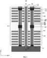
- FIG. 1 illustrates a cross-sectional view of a memory device 100 (e.g., a 3D memory device), according to some embodiments of the present disclosure.
- Memory device 100 may include a memory stack 104, which includes a plurality of memory decks. For ease of illustration, two memory decks 104A and 104B are depicted and described in FIG. 1 .
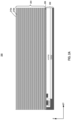
- FIGs. 2A-2I illustrates a fabrication process of one memory deck (e.g., 104A), according to some embodiments of the present disclosure.
- FIG. 3 illustrates a fabrication process of a memory string having a semiconductor plug in a memory deck (e.g., 104A), according to some embodiments of the present disclosure.
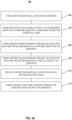
- FIG. 4A is a flowchart of the fabrication process illustrated in FIGs. 2A-2I , according to some embodiments of the present disclosure.
- FIG. 4B illustrates a flowchart of a fabrication process for forming a dual-deck memory device (e.g., memory device 100),
- memory device 100 includes a substrate 102, a bottom dielectric layer 118 over substrate 102, and memory stack 104 over bottom dielectric layer 118.
- Memory deck 104 may include two memory decks 104A (e.g., a lower memory deck) and 104B (e.g., an upper memory deck) stacking together along a direction (e.g., the vertical direction or the z-direction) perpendicular to a top surface of substrate 102.
- Each memory deck (e.g., 104A or 104B) includes a plurality of interleaved dielectric layers 110a and conductor layers 110b extending along a direction (e.g., a lateral direction or the x-y plane) parallel to the top surface of substrate 102.
- a direction e.g., a lateral direction or the x-y plane
- a thickness (e.g., along the vertical direction) of bottom dielectric layer 118 may be about 10 nm to about 50 nm, such as between 20 nm and 50 nm, (e.g., 15 nm, 20 nm, 25 nm, 30 nm, 35 nm, 40 nm, 45 nm, 50 nm, any range bounded by the lower end by any of these values, or in any range defined by any two of these values).
- Memory deck 104 includes a plurality of memory strings 108 each extending vertically through memory stack 104 and bottom dielectric layer 118, to connect to substrate 102, which includes a heavy doped region, e.g., a heavy P-well (not shown in FIG. 1 ) at a top portion of substrate 102, conductively connected to memory strings 108.
- Memory string 108 may include a plurality of (e.g., two) memory sub-strings (e.g., 108-1 and 108-2), each extending through the respective memory deck (e.g., 104A and 104B).
- the adjacent memory sub-strings may be aligned along the vertical direction (e.g., extending direction of memory strings 108) and may be conductively connected by a channel plug 108f, which includes a conductive material such as poly-silicon or amorphous silicon.
- Memory string 108 may include a top channel plug 112 at an upper portion of memory string 108, a top doped region 114 in top channel plug 112, and a semiconductor plug 108g at a lower portion of memory string 108.
- Top channel plug 112 and top doped region 114 may form conductive connection to other devices/circuits such as peripheral devices.
- Semiconductor plug 108g may form conductive connection to the heavy doped region in substrate 102.
- Memory string 108 may include a channel structure that includes a blocking layer 108a, a memory layer 108b, a tunneling layer 108c, a semiconductor layer 108d (e.g., also referred to as a semiconductor channel 108d), and a dielectric core 108e, sequentially arranged from a sidewall to a center of memory string 108.
- a semiconductor channel (not shown) is formed in the semiconductor layer, conductively connected to semiconductor plug 108g and top channel plug 112, for carrier transport when memory device 100 is in operation.
- Memory deck 104 may also include a source structure 106 extending vertically through memory stack 104 and bottom dielectric layer 118 and into substrate 102.
- Source structure 106 may include a doped semiconductor region 106a, an insulating structure 106b extending through memory stack 104 and covering conductor layers 110b, and a source conductor 106c extending in insulating structure 106b and being conductively connected to doped semiconductor region 106a.
- Source structure 106 may also include a source plug 116 in an upper portion of source conductor 106c for conductively connecting to other devices/circuits (e.g., peripheral devices).
- Memory device 100 can be part of a monolithic 3D memory device.
- monolithic means that the components (e.g., the peripheral device and memory array device) of the 3D memory device are formed on a single substrate.
- the fabrication encounters additional restrictions due to the convolution of the peripheral device processing and the memory array device processing.
- the fabrication of the memory array device e.g., memory strings
- memory device 100 can be part of a non-monolithic 3D memory device, in which components (e.g., the peripheral device and memory array device) can be formed separately on different substrates and then bonded, for example, in a face-to-face manner.
- the memory array device substrate e.g., substrate 102
- the peripheral device e.g., including any suitable digital, analog, and/or mixed-signal peripheral circuits used for facilitating the operation of memory device 100, such as page buffers, decoders, and latches; not shown
- the memory array device e.g., memory strings
- the memory array device substrate (e.g., substrate 102) is flipped and faces down toward the peripheral device (not shown) for hybrid bonding, so that in the bonded non-monolithic 3D memory device, the memory array device is above the peripheral device.
- the memory array device substrate (e.g., substrate 102) can be a thinned substrate (which is not the substrate of the bonded non-monolithic 3D memory device), and the back-end-of-line (BEOL) interconnects of the non-monolithic 3D memory device can be formed on the backside of the thinned memory array device substrate.
- Substrate 102 can include silicon (e.g., single crystalline silicon), silicon germanium (SiGe), gallium arsenide (GaAs), germanium (Ge), silicon on insulator (SOI), germanium on insulator (GOI), or any other suitable materials.
- substrate 102 is a thinned substrate (e.g., a semiconductor layer), which was thinned by grinding, etching, chemical mechanical polishing (CMP), or any combination thereof.
- substrate 102 includes a heavy doped region such as a heavy P-well that includes doped silicon, in the upper portion of substrate 102 and contacting memory strings 108.
- memory device 100 is a NAND Flash memory device in which memory cells are provided in the form of an array of memory strings 108 (e.g., memory strings) extending vertically above substrate 102.
- the memory array device can include memory strings 108 that extend through a plurality of pairs each including a conductor layer 110b and a dielectric layer 110a (referred to herein as "conductor/dielectric layer pairs").
- the stacked conductor/dielectric layer pairs are also referred to herein as a "memory deck” 104.
- the number of the conductor/dielectric layer pairs in memory stack 104 determines the number of memory cells in memory device 100.
- Memory stack 104 includes a plurality of interleaved conductor layers 110b and dielectric layers 110a.
- Conductor layers 110b and dielectric layers 110a in memory stack 104 can alternate in the vertical direction.
- Conductor layers 110b can include conductive materials including, but not limited to, tungsten (W), cobalt (Co), copper (Cu), aluminum (Al), polysilicon, doped silicon, silicides, or any combination thereof.
- Dielectric layers 110a can include dielectric materials including, but not limited to, silicon oxide, silicon nitride, silicon oxynitride, or any combination thereof.
- the numbers of conductor/dielectric layer pairs in each of lower and upper memory decks 104A and 104B can be the same or different.
- memory string 108 can include a channel structure extending vertically through memory stack 104.
- the channel structure can include a channel hole filled with semiconductor material(s) (e.g., as a semiconductor channel 108d) and dielectric material(s) (e.g., as blocking layer 108a, memory layer 108b, and tunneling layer 108c).
- semiconductor channel 108d includes silicon, such as amorphous silicon, polysilicon, or single crystalline silicon.
- the remaining space of the channel structure can be partially or fully filled with dielectric core 108e including dielectric materials, such as silicon oxide.
- the channel structure can have a cylinder shape (e.g., a pillar shape).
- Dielectric core 108e, semiconductor channel 108d, tunneling layer 108c, memory layer 108b, and blocking layer 108a are arranged radially from the center toward the outer surface of the pillar in this order, according to some embodiments.
- Tunneling layer 108c can include silicon oxide, silicon oxynitride, or any combination thereof.
- Memory layer 108b can include silicon nitride, silicon oxynitride, silicon, or any combination thereof.
- Blocking layer 108a can include silicon oxide, silicon oxynitride, high dielectric constant (high-k) dielectrics, or any combination thereof.
- tunneling layer 108c/memory layer 108b/blocking layer 108a can include a composite layer of silicon oxide/silicon oxynitride/silicon oxide (ONO).
- conductor layer 110b (each being part of a word line) in memory stack 104 functions as a gate conductor of memory cells in memory string 108.
- Conductor layer 110b can include multiple control gates of multiple memory cells and can extend laterally as a word line ending at the edge of memory stack 104 (e.g., in a staircase structure of memory stack 104).
- memory cell transistors in memory string 108 include gate conductors (i.e., parts of conductor layers 110b that abut the channel structure) made from W, adhesion layers (not shown) including titanium/titanium nitride (Ti/TiN) or tantalum/tantalum nitride (Ta/TaN), gate dielectric layers (not shown) made from high-k dielectric materials, and the channel structure including polysilicon.
- Bottom conductor layer 110b e.g., conductor layer 110b that is closest to substrate 102 functions as a bottom select gate and intersects and contacts the channel structure (e.g., memory string 108).
- memory string 108 further includes semiconductor plug 108g in a lower portion (e.g., at the lower end) of memory string 108.
- semiconductor plug 108g in a lower portion (e.g., at the lower end) of memory string 108.
- the "upper end" of a component e.g., memory string 108 is the end farther away from substrate 102 in the y-direction
- the "lower end” of the component e.g., memory string 108
- Semiconductor plug 108g includes poly-silicon or amorphous silicon, which is deposited on substrate 102 in any suitable directions.
- the top surface of semiconductor plug 108g is lower, e.g., along the vertical direction, than the top surface of bottom conductor layer 110b.
- Semiconductor plug 108g can function as a channel controlled by a source select gate of memory string 108.
- conductor layers 110b e.g., bottom conductor layer 110b intersect and contact memory string 108.
- memory string 108 further includes a top channel plug 112 in an upper portion (e.g., at the upper end) of memory string 108.
- Top channel plug 112 can be in contact with the upper end of semiconductor channel 108d.
- Top channel plug 112 can include semiconductor materials (e.g., polysilicon) or conductive materials (e.g., metals).
- top channel plug 112 includes an opening filled with Ti/TiN or Ta/TaN as an adhesion layer and tungsten as a conductor. By covering the upper end of the channel structure during the fabrication of memory device 100, top channel plug 112 can function as an etch stop layer to prevent etching of dielectrics filled in the channel structure, such as silicon oxide and silicon nitride.
- top channel plug 112 also functions as the drain of memory string 108.
- a top doped region 114 is formed in top channel plug 112 to increase conductivity.
- source structure 106 may extend vertically through memory stack 104 and be conductively connected to substrate 102.
- Doped semiconductor region 106a may be conductively connected to a heavy doped region/well (e.g., a heavy P-well in substrate 102, not shown) so source conductor 106c can be conductively connected to memory strings 108.
- Source conductor 106c can include any suitable conductive material such as W, Co, Al, Cu, polysilicon, and/or silicide.
- Insulating structure 106b can include any suitable dielectric materials such as silicon oxide.
- source plug 116 e.g., a doped region
- source conductor 106c when source conductor 106c includes polysilicon, source plug 116 (e.g., a doped region) is formed in the upper portion of source conductor 106c to increase conductivity of source conductor 106c with other devices/circuits.
- FIGs. 2A-2I illustrate an exemplary fabrication process to form a lower memory deck
- FIG. 3 illustrates an exemplary fabrication process to form a memory string with a "SEG-free" semiconductor plug in structures depicted in FIGs. 2A-2I
- FIG. 4A illustrates a flowchart of an exemplary method 400 for forming the lower memory deck
- FIG. 4B illustrates a flowchart of an exemplary method 450 for forming memory device 100.
- the fabrication processes are now described in view of the structures shown in FIGs. 2A-2I and 3 . It is understood that the operations shown in methods 400 and 450 are not exhaustive and that other operations can be performed as well before, after, or between any of the illustrated operations. Further, some of the operations may be performed simultaneously, or in a different order than shown in FIGs. 2A-2I , 3 , 4A and 4B .
- FIG. 4A at the beginning of the process, a bottom sacrificial layer is formed over a substrate and a dielectric deck is formed over the bottom sacrificial layer.
- the dielectric deck includes a plurality of interleaved sacrificial layers and dielectric layers (Operations 402 and 404).
- FIGs. 2A-2C illustrate corresponding structures.
- an initial bottom sacrificial layer 206 may be formed over a substrate 202, and an initial dielectric deck 204 may be formed over initial bottom sacrificial layer 206.
- substrate 202 can be a silicon substrate that includes a plurality of doped wells such at the upper portion of substrate 202.
- the doped wells can include a heavy P-well (HVPW), a deep N-well (DNW), and a heavy N-well (HVNW), as shown in FIG. 2A .
- the HVPW is located under the subsequently-formed memory strings formed in the dielectric deck.
- the doped wells can be formed by respective ion implantation processes on substrate 202.
- initial bottom sacrificial layer 206 includes a suitable material different from the material of the sacrificial layers of initial dielectric deck 204.
- the material of initial bottom sacrificial layer 206 may have sufficiently high etching selectivity over initial dielectric deck 204.
- initial bottom sacrificial layer 206 functions as an etch stop layer to stop the etching of initial dielectric deck 204.
- initial bottom sacrificial layer 206 includes one or more of W, Co, Al, and Cu.
- Initial bottom sacrificial layer 206 may be formed by any suitable deposition process such as sputtering, electron beam evaporation, chemical vapor deposition (CVD), and/or physical vapor deposition (PVD).
- initial bottom sacrificial layer 206 can be planarized (e.g., by recess etch and/or chemical mechanical polishing (CMP)) to ensure desirable flatness for initial dielectric deck 204 to be formed thereon.
- CMP chemical mechanical polishing
- Initial dielectric deck 204 can include a first plurality of interleaved initial dielectric layers 210a and initial sacrificial layers 210b.
- An initial sacrificial layer 210b and its respective initial dielectric layer 210a (e.g., dielectric layer 210a over or under it) can together be referred to herein as an "initial dielectric layer pair.
- Initial dielectric layers 210a and initial sacrificial layers 210b can be alternatively deposited on initial bottom sacrificial layer 206 to form initial dielectric deck 204.
- each initial dielectric layer 210a includes a layer of silicon oxide
- each initial sacrificial layer 210b includes a layer of silicon nitride.
- each initial dielectric layer 210a and each initial sacrificial layer 210b have nominally the same thicknesses along the vertical direction.
- the thickness of initial bottom sacrificial layer 206 may be similar to or in a similar range (e.g., between 10 nm and 70nm). In some embodiments, the thicknesses of initial dielectric layer 210a, initial sacrificial layer 210b, and initial bottom sacrificial layer 206 may have nominally the same thickness.
- Initial dielectric deck 204 can be formed by one or more thin film deposition processes including, but not limited to, CVD, PVD, atomic layer deposition (ALD), or any combination thereof. In some embodiments, initial bottom sacrificial layer 206 and initial dielectric deck 204 covers the area of the HVPW on substrate 202.
- a dielectric deck 214 can be formed over initial bottom sacrificial layer 206.
- Dielectric deck 214 can be formed by, e.g., repetitively etching the initial dielectric layer pairs along the vertical direction and lateral directions.
- an etch mask e.g., a photoresist layer (not shown) can be patterned over the top surface of initial dielectric deck 204.
- the etch mask can be repetitively trimmed (e.g., etched) laterally (e.g., along various directions parallel to the lateral/ x - y plane) and vertically to expose portions of initial dielectric deck 204.
- a suitable isotropic etching process may be performed to repetitively remove the exposed portions of initial dielectric deck 204 along various directions.
- initial bottom sacrificial layer 206 functions as an etch stop layer such that the etching rate of initial dielectric deck 204 is sufficiently higher than the etching rate of initial bottom sacrificial layer 206.
- dielectric deck 214 may be formed over initial bottom sacrificial layer 206.
- dielectric deck 214 includes a staircase structure. Initial dielectric layer pairs can be etched to form dielectric layer pairs that each includes a dielectric layer 220a and a sacrificial layer 220b.
- the portion of initial bottom sacrificial layer 206 exposed by dielectric deck 214 may be removed to form bottom sacrificial layer 216 and expose substrate 202.
- the removal of the exposed portion of initial bottom sacrificial layer 206 can include any suitable etching process such as a wet etch or wet clean process.
- a dielectric filling material can then be deposited over substrate 202 and dielectric deck 214 and planarized to form a dielectric filling structure 222.
- a memory string is formed.
- the memory string extends through the dielectric deck and the bottom sacrificial layer, and contacts the substrate (Operation 406).
- FIGs. 2D and 2E illustrate corresponding structures.
- a plurality of openings 230 can be formed to extend through dielectric deck 214 to expose bottom sacrificial layer 216, and a layer of a blocking material 230a, a layer of a memory material 230b, a layer of a tunneling material 230c, and a layer of a semiconductor material 230d can be sequentially deposited over a sidewall of opening 230. Because bottom sacrificial layer 216 functions as an etch stop layer, a bottom surface of opening 230 may expose bottom sacrificial layer 216.
- Opening 230 may be formed by a suitable etching process using a patterned etch mask that exposes areas corresponding to opening 230 over dielectric deck 214.
- the etching process includes dry etch. Any suitable deposition processes, e.g., CVD, PVD, ALD, and/or sputtering, can be performed to deposit the layers of blocking material 230a, memory material 230b, tunneling material 230c, and semiconductor material 230d.
- a memory string 240 can be formed from an opening 230 and channel-forming layers (e.g., 230a, 230b, 230c, and 230d) deposited in opening 230.
- Memory string 240 may include a blocking layer 240a, a memory layer 240b, a tunneling layer 240c, a semiconductor layer 240d, and a dielectric core 240e arranged sequentially from the sidewall to the center of opening 230.
- Memory string 240 may also include a channel plug 240f over and conductively connected to these layers, and a semiconductor plug 240g at the bottom of memory string 240, conductively connected to these layers and substrate 202.
- memory string 240 is similar to or the same as memory sub-string 108-1. The fabrication process of memory string 240 is described in detail as follows in view of FIG. 3 .
- a support pillar is formed.
- the support pillar extends through the dielectric deck and the bottom sacrificial layer to contact the substrate (Operation 408).
- FIGs. 2F and 2G illustrate corresponding structures.
- a plurality of support pillars 252 are formed to extend through dielectric deck 214, dielectric filling structure 222 and bottom dielectric layer 216, to contact substrate 202.
- a support pillar 252 includes a pillar hole that extends through dielectric deck 214, dielectric filling structure 222, and bottom dielectric layer 216 to expose substrate 202, and a pillar material (e.g., a dielectric material such as silicon oxide) filled in the pillar hole.
- a lateral dimension (e.g., diameter) of support pillar 252 is less than a lateral dimension (e.g., diameter) of memory string 240.
- Support pillars 252 can be formed by performing a suitable etching process (e.g., a dry etch) using a patterned etch mask that exposes areas corresponding to the pillar holes.
- a suitable etching process e.g., a dry etch
- an initial slit structure 256 is formed by the same etching process that forms the pillar holes.
- Initial slit structure 256 may extend through dielectric deck 214, dielectric filling structure 222 and bottom dielectric layer 216 to expose substrate 202.
- a suitable dielectric material can be deposited to fill up the pillar holes with any suitable deposition process such as CVD, PVD, and/or ALD.
- a layer of the pillar-filling dielectric material 254 can be deposited over a bottom surface and a sidewall of initial slit structure 256 and on dielectric deck 214.
- FIG. 2G illustrates a corresponding structure.
- the portions of pillar-filling dielectric material 254 on the sidewall and on the bottom surface of initial slit structure 256 can be removed to expose substrate 202 and the remaining portion of bottom dielectric layer 216 (i.e., the portion of bottom dielectric layer 216 retained from the formation of initial slit structure 256). The remaining portion of bottom dielectric layer 216 can then be removed.
- An initial bottom dielectric layer 266 can be formed between dielectric deck 214 and substrate 202. In some embodiments, initial bottom dielectric layer 266 fills up the space between dielectric deck 214 and substrate 202, and forms a layer at the bottom of initial slit structure 256.
- the portions of pillar-filling dielectric material 254 on the sidewall and bottom surface of initial slit structure 256 can be removed by covering the top surface of dielectric deck 214 with a protective layer and perform a suitable etching process to remove the portions of pillar-filling dielectric material 254 on the sidewall and bottom surface of initial slit structure 256.
- the protective layer includes polymer
- the etching process includes a dry etch.
- a suitable wet etch can be performed to remove bottom sacrificial layer 216.
- the wet etch has sufficiently high etching selectivity of bottom sacrificial layer 216 over dielectric deck 214 and support pillars 252 so that little or no damage is formed on the sidewall of initial slit structure 256 (or dielectric deck 214).
- support pillars 252 remain through dielectric filling structure 222 and dielectric deck 214 to substrate 202 after bottom sacrificial layer 216 is removed. That is, support pillars 252 may support dielectric deck 214 on substrate 202 during and after the etching of bottom sacrificial layer 216.
- Initial bottom dielectric layer 266 is formed between dielectric deck 214 and substrate 202.
- Initial bottom dielectric layer 266 can be formed in a suitable process such as one or more of a "native oxide” method, an "in-situ steam generated (ISSG) oxidation” method, and a silane oxidation method.
- the native oxide method includes an oxidation process involving oxygen gas and substrate 202 to form a native oxide (e.g., silicon oxide) of substrate 202 along the vertical direction until the space formed by the removal of bottom sacrificial layer 216 is filled with the native oxide.
- the ISSG oxidation method includes a thermal oxidation process involving reactant gases of hydrogen, oxygen, and substrate 202 to form silicon oxide along the vertical direction until the space formed by the removal of bottom sacrificial layer 216.
- the silane oxidation method includes a thermal oxidation process involving reactant gases of silane (SiH 4 ) and oxygen to form silicon oxide along the vertical direction until the space formed by the removal of bottom sacrificial layer 216.
- initial bottom dielectric layer 266 may extend along the top surface of substrate 202 and under dielectric deck 214.
- FIG. 4A a source structure is formed to extend through the dielectric deck and into the substrate (Operation 412).
- FIGs. 2H and 2I illustrate corresponding structures.
- Initial memory deck 274 can be formed.
- Initial memory deck 274 may include a slit structure 276 extending through initial memory deck 274 and exposing initial bottom dielectric layer 266, a plurality of recessed conductor layers 270b extending laterally on the sidewall of slit structure 276, and a doped semiconductor region 278 in the portion of HVPW that is under slit structure 276.
- sacrificial layers 220b of dielectric deck 214 are replaced with a plurality of conductor layers extending laterally, and a slit structure 276 may be formed by performing a recess etch on the conductor layers exposed in initial slit structure 256.
- a suitable etching process e.g., a wet etch
- a suitable deposition process e.g., CVD, PVD, ALD, and/or sputtering
- CVD, PVD, ALD, and/or sputtering is performed to deposit a conductive material to fill up the lateral recesses and form a plurality of conductor layers.
- the conductor layers can include one or more of W, Co, Al, and Cu.
- an adhesive layer including Ti and/or TiN can be formed prior to the deposition of the conductor layers between adjacent dielectric layers 220a to increase the adhesion between the conductor layers and adjacent dielectric layers 220b.
- the recess etch can be performed on the conductor layers to form the plurality of recessed conductor layers 270b.
- a plurality of recessed conductor layers 270b and a plurality of recesses 276a abutting the sidewall of slit structure 276 are formed by etching parts of the conductor layers of dielectric deck 214 that abut the sidewall of initial slit structure 256.
- recesses 276a are formed by applying etchants to the conductor layers through initial slit structure 256 to completely remove part of the conductor layers along the sidewall of initial slit structure 256 and further etch parts of the conductor layers in the lateral recesses.
- Recessed conductor layers 270b, slit structure 276, and initial memory deck 274 can be formed.
- the dimension of recess 276a can be controlled by the etching rate (e.g., based on the etchant temperature and concentration) and/or etching time.
- Recessed conductor layers 270b can subsequently function as the gate lines of memory device 200.
- Doped semiconductor region 278 can be formed by performing an ion implantation process on the portion of initial bottom dielectric layer 266 exposed by slit structure 276 before or after the formation of recessed conductor layers 270b. Doped semiconductor region 278 can subsequently function as a common source of the surrounded memory strings 240. Doped semiconductor region 278 may be conductively connected to the surrounded memory strings 240 through the HVPW.
- Source structure 286 is formed in slit structure 276 and a memory deck 284 can be formed.
- Source structure 286 may include an insulating structure 286b (e.g., a spacer) along a sidewall of slit structure 276 to cover recessed conductor layers 270b and electrically separate recessed conductor layers 270b of the memory stack.
- insulating structure 286b includes a dielectric material is formed along the sidewall of slit structure 276 and in recesses 276a using one or more thin film deposition processes, such as ALD, CVD, PVD, any other suitable processes, or any combination thereof.
- Insulating structure 286b can include a single or composite layer of dielectric materials, such as silicon oxide and silicon nitride. By covering the sidewall of slit structure 276 as well as filling in recesses 276a with insulating structure 286b, recessed conductor layers 270b (e.g., gate lines) of memory deck 284 can be electrically separated by insulating structures 286b.
- dielectric materials such as silicon oxide and silicon nitride.
- a source contact 286a is formed in insulating structure 286b and through initial bottom dielectric layer 266 in slit structure 276.
- Source contact 286a may be in contact with doped semiconductor region 278 and may be conductively connected to the surrounded memory strings 240 through doped semiconductor region 278.
- a suitable etching process e.g., dry etch
- Source contact 286a can be formed by depositing a suitable conductive material over insulating structure 286b.
- the conductive materials may include, but not limited to, W, Co, Cu, Al, polysilicon, silicides, or any combination thereof, using one or more thin film deposition processes, such as ALD, CVD, PVD, any other suitable processes, or any combination thereof.
- Source contact 286a can act as an array common source (ACS) contact electrically connected to the channel structures of surrounded memory strings 240.
- Source structure 286 including insulating structure 286b and source contact 286a can thereby be formed in slit structure 276, surrounded by a plurality of memory strings 240.
- a planarization process (e.g., CMP and/or recess etch) can be performed to remove any excessive conductive material that forms source contact 286a and/or dielectric material that forms insulating structure 286b.
- An insulating cap layer 288 can be formed over memory deck 284. In some embodiments, insulating cap layer 288 provides the base for other devices/structures (e.g., another memory deck) to be formed over memory deck 284.
- FIG. 3 illustrates operations A-H for forming a memory string 240 with a semiconductor plug 240g, according to some embodiments.
- layers of tunneling material and semiconductor material i.e., 230c and 230d
- tunneling layer 240c and semiconductor layer 240d are shown as one single layer in operations F-H.
- a layer of semiconductor material 230d is deposited over layer of tunneling material 230c
- semiconductor layer 240d is over tunneling layer 240c.
- channel-forming layers e.g., a layer of a blocking material 230a, a layer of a memory material 230b, a layer of a tunneling material 230c, and a layer of a semiconductor material 230d may be sequentially deposited over the sidewall of opening 230 in dielectric deck 214.
- an initial plug opening 234a may be formed through layers of blocking material, memory material, tunneling material, and semiconductor material (i.e., 230a, 230b, 230c, and 230d) to expose bottom sacrificial layer 216.
- a suitable dry etching process can be performed to remove portions of the channel-forming layers.
- a plug opening 234 can be formed.
- Plug opening 234 can be formed by enlarging or expanding initial plug opening 234a to vertically and laterally remove materials surrounding initial plug opening 234a.
- Plug opening 234 can be through bottom sacrificial layer 216 and can expose the HVPW under bottom sacrificial layer 216.
- a suitable etching process e.g., wet etch
- the etching process may be isotropic so that the materials surrounding initial plug opening 234a are removed vertically and laterally until the desired dimensions of plug opening 234 are reached and/or the HVPW is exposed.
- plug opening 234 is under layers of blocking material, memory material, tunneling material, and semiconductor material (i.e., 230a, 230b, 230c, and 230d) and exposing HVPW of substrate 202.
- the sidewalls of plug opening 234 laterally expands into layer of blocking material 230a.
- a top surface of plug opening 234 is below a top surface of the initial bottom sacrificial layer 210b (i.e., the sacrificial layer directly above and in contact of bottom sacrificial layer 216).
- another layer of the semiconductor material e.g., polysilicon
- Semiconductor plug 240g can be formed. Any suitable deposition process, e.g., CVD, PVD, ALD, and/or sputtering, can be employed to form semiconductor plug 240g. Optionally, the deposition process can form air gaps 246 in semiconductor plug 240g.
- Semiconductor plug 240g may be conductively connected to a layer of semiconductor material 230d and HVPW.
- a layer of a dielectric core material 230e can be deposited, employing any suitable deposition methods such as CVD, PVD, ALD, and/or sputtering, to fill up opening 230.
- a suitable planarization process e.g., CMP and/or recess etch
- CMP and/or recess etch can be performed to remove layers of the dielectric core material 230e, and layers of semiconductor material 230d and tunneling material 230c so that layer of memory material 230b can be exposed.
- a suitable etching process e.g., dry etch and/or wet etch
- a layer of conductive material 232 is deposited to fill up the channel-plug opening.
- Layer of conductive material 232 may be deposited using any suitable deposition methods such as CVD, PVD, ALD, and/or sputtering.
- the etched layers of memory material, tunneling material, semiconductor material, and dielectric core material can then form memory layer 240b, tunneling layer 240c, semiconductor layer 240d, and dielectric core 240e.
- the layer of blocking material 230a can form blocking layer 240a.
- a planarization process e.g., CMP and/or recess etch
- Memory string 240 including blocking layer 240a, memory layer 240b, tunneling layer 240c, semiconductor layer 240d, channel plug 240f, and semiconductor plug 240g, can be formed.
- a layer of insulating material can be deposited to cover memory string 240.
- a planarization process e.g., CMP and/or recess etch
- CMP and/or recess etch can be performed to remove excessive portions of the insulating material and form insulating cap layer 244 over dielectric deck 214.
- FIG. 4B illustrates a flowchart to form an exemplary 3D memory device (e.g., memory device 100) having a plurality of memory decks stacking along the vertical direction, according to some embodiments.
- memory device 100 having a lower memory deck (e.g., a first memory deck) and an upper memory deck (e.g., a second memory deck), is described as an example.
- the operations described in FIGs. 2A-2I and FIG. 4A illustrate the fabrication process to form the lower memory deck 104A (e.g., first memory deck) from a first dielectric deck 214.
- FIG. 4B illustrate the fabrication process to form an upper memory deck 104B (e.g., the second memory deck) from a second dielectric deck.
- the operations to form more memory decks over the upper memory deck should be similar to the processes to form the lower and the upper memory decks and are not repeated herein.
- the lower and upper memory decks can each be referred to as a memory deck of memory device 100, and the memory strings (e.g., 108-1 and 108-2) in each memory deck can each be referred to as memory sub-strings.
- a bottom sacrificial layer may be formed over a substrate, and a first dielectric deck having a plurality of interleaved sacrificial layers and dielectric layers can be formed over the bottom sacrificial layer.
- the fabrication process can be similar to or the same as the fabrication process illustrated in FIGs. 2A-2C .
- the first dielectric deck is fabricated to subsequently form first memory deck 104A.
- a first memory string extending through the first dielectric deck and the bottom sacrificial layer and contacting the substrate, can be formed.
- the fabrication process can be similar to or the same as the fabrication process illustrated in FIGs. 2D-2E and FIG. 3 .
- the first memory string corresponds to memory sub-string 108-1 and includes a channel plug (e.g., 108f) at the upper portion, a semiconductor plug 108g at the lower portion and conductively connected to the substrate, and a semiconductor channel conductively connected to semiconductor plug 108g and channel plug 108f.
- a channel plug e.g., 108f
- a second dielectric deck having a plurality of second interleaved sacrificial layers and dielectric layers can be formed over the first dielectric deck.
- the formation of the second dielectric deck can be the same as or similar to the formation of the first dielectric deck.
- the second dielectric deck is fabricated to subsequently form second memory deck 104B.
- a second memory string, extending through the second dielectric deck and connecting with the first memory string can be formed.
- the second memory string corresponds to memory sub-string 108-2, which is aligned with memory sub-string 108-1 along the vertical direction.
- the fabrication process can be similar to or the same as the fabrication process illustrated in FIGs. 2D-2E . Different from the fabrication process shown in FIGs. 2D-2E , no semiconductor plug is formed in second memory deck 104B, and the semiconductor channel of the second memory string is conductively connected to the channel plug of the first memory string.
- the bottom sacrificial layer can be replaced with a bottom dielectric layer between the first dielectric deck and the substrate.
- the fabrication process can be similar to or the same as the fabrication process illustrated in FIGs. 2F-2G .
- an initial slit structure is formed extending through the first and second dielectric decks to expose the substrate, e.g., for the replacement of bottom sacrificial layer and subsequent operations.
- a source structure extending through the first and the second memory decks and into the substrate, can be formed.
- the plurality of first and second sacrificial layers are replaced with a plurality of conductor layers before the formation of the source structure.
- the first dielectric deck and the second dielectric deck can respectively form the first memory deck (e.g., 104A) and the second memory deck (e.g., 104B).
- the fabrication process to form the conductor layers, the first and the second memory decks, and the source structure can be similar to or the same as the fabrication process illustrated in FIGs. 2H-2I .
- a top doped region (e.g., 114) and/or a source plug (e.g., 116) are respectively formed in the upper portions of channel plug (e.g., 112) and source plug 116 by a suitable ion implantation and/or a deposition of a conductive material in a recessed portion of the channel plug and the source conductor.
Landscapes
- Semiconductor Memories (AREA)
- Non-Volatile Memory (AREA)
Description
- Embodiments of the present disclosure relate to three-dimensional (3D) memory devices and fabrication methods thereof.
- Planar memory cells are scaled to smaller sizes by improving process technology, circuit design, programming algorithm, and fabrication process. However, as feature sizes of the memory cells approach a lower limit, planar process and fabrication techniques become challenging and costly. As a result, memory density for planar memory cells approaches an upper limit.
- A 3D memory architecture can address the density limitation in planar memory cells. The 3D memory architecture includes a memory array and peripheral devices for controlling signals to and from the memory array.
- Embodiments of 3D memory devices with deposited semiconductor plugs and methods for forming the same are disclosed herein. A three-dimensional memory device according to the invention is presented in claim 1.
- In one example, a 3D memory device includes a substrate, a memory deck, and a memory string. The memory deck includes a plurality of interleaved conductor layers and dielectric layers on the substrate. The memory string extends vertically through the memory deck. A bottom conductor layer of the plurality of interleaved conductor layers and dielectric layers intersects with and contacts the memory string.
- In another example, a 3D memory device includes a substrate, a memory stack, and a memory string. The memory stack includes a plurality of memory decks each having a plurality of interleaved conductor layers and dielectric layers over the substrate. The memory string includes a plurality of memory sub-strings extending vertically through the memory stack, each memory deck having a respective memory sub-string. A bottom conductor layer of the plurality of interleaved conductor layers and dielectric layers intersects with and contacts the memory string.
- In still another example, a method for forming a 3D memory device includes the following operations. First, a bottom sacrificial layer is formed over a substrate. A dielectric deck having a plurality of interleaved sacrificial layers and dielectric layers is formed over the bottom sacrificial layer. A memory string is then formed extending through the dielectric deck and the bottom sacrificial layer and contacting the substrate. A support pillar is formed extending through the dielectric deck and the bottom sacrificial layer to contact the substrate. Further, the bottom sacrificial layer is replaced with a bottom dielectric layer between the dielectric deck and the substrate. A source structure is then formed extending through the dielectric deck and into the substrate.
- In a further example, a method for forming a 3D memory device includes the following operations. First, a bottom sacrificial layer is formed over a substrate. A first dielectric deck having a plurality of first interleaved sacrificial layers and dielectric layers is formed over the bottom sacrificial layer. A first memory string is formed extending through the first dielectric deck and the bottom sacrificial layer and contacting the substrate. A second dielectric deck having a plurality of second interleaved sacrificial layers and dielectric layers is then formed over the first dielectric deck. A second memory string is formed extending through the second dielectric deck and conductively connecting with the first memory string. The bottom sacrificial layer is replaced with a bottom dielectric layer between the first dielectric deck and the substrate. The plurality of first and second sacrificial layers is then replaced with a plurality of conductors to form a first and a second memory decks. A source structure is formed extending through the first and the second memory decks and into the substrate.
- The accompanying drawings, which are incorporated herein and form a part of the specification, illustrate embodiments of the present disclosure and, together with the description, further serve to explain the principles of the present disclosure and to enable a person skilled in the pertinent art to make and use the present disclosure.
-
FIG. 1 illustrates a cross-sectional view of an exemplary 3D memory device, according to some embodiments of the present disclosure. -
FIGs. 2A-2I illustrate cross-section views of an exemplary 3D memory device at various stages of an exemplary fabrication process, according to some embodiments of the present disclosure. -
FIG. 3 illustrates an exemplary fabrication process to form a memory string, according to some embodiments of the present disclosure. -
FIGs. 4A-4B each illustrates a flowchart of an exemplary method for forming a 3D memory device, according to some embodiments of the present disclosure. - Embodiments of the present disclosure will be described with reference to the accompanying drawings.
- Although specific configurations and arrangements are discussed, it should be understood that this is done for illustrative purposes only. A person skilled in the pertinent art will recognize that other configurations and arrangements can be used without departing from the scope of the present disclosure. It will be apparent to a person skilled in the pertinent art that the present disclosure can also be employed in a variety of other applications.
- It is noted that references in the specification to "one embodiment," "an embodiment," "an example embodiment," "some embodiments," etc., indicate that the embodiment described may include a particular feature, structure, or characteristic, but every embodiment may not necessarily include the particular feature, structure, or characteristic. Moreover, such phrases do not necessarily refer to the same embodiment. Further, when a particular feature, structure or characteristic is described in connection with an embodiment, it would be within the knowledge of a person skilled in the pertinent art to effect such feature, structure or characteristic in connection with other embodiments whether or not explicitly described.
- In general, terminology may be understood at least in part from usage in context. For example, the term "one or more" as used herein, depending at least in part upon context, may be used to describe any feature, structure, or characteristic in a singular sense or may be used to describe combinations of features, structures or characteristics in a plural sense. Similarly, terms, such as "a," "an," or "the," again, may be understood to convey a singular usage or to convey a plural usage, depending at least in part upon context. In addition, the term "based on" may be understood as not necessarily intended to convey an exclusive set of factors and may, instead, allow for existence of additional factors not necessarily expressly described, again, depending at least in part on context.
- It should be readily understood that the meaning of "on," "above," and "over" in the present disclosure should be interpreted in the broadest manner such that "on" not only means "directly on" something but also includes the meaning of "on" something with an intermediate feature or a layer therebetween, and that "above" or "over" not only means the meaning of "above" or "over" something but can also include the meaning it is "above" or "over" something with no intermediate feature or layer therebetween (i.e., directly on something).
- Further, spatially relative terms, such as "beneath," "below," "lower," "above," "upper," and the like, may be used herein for ease of description to describe one element or feature's relationship to another element(s) or feature(s) as illustrated in the figures. The spatially relative terms are intended to encompass different orientations of the device in use or operation in addition to the orientation depicted in the figures. The apparatus may be otherwise oriented (rotated 90 degrees or at other orientations) and the spatially relative descriptors used herein may likewise be interpreted accordingly.
- As used herein, the term "substrate" refers to a material onto which subsequent material layers are added. The substrate itself can be patterned. Materials added on top of the substrate can be patterned or can remain unpatterned. Furthermore, the substrate can include a wide array of semiconductor materials, such as silicon, germanium, gallium arsenide, indium phosphide, etc. Alternatively, the substrate can be made from an electrically non-conductive material, such as a glass, a plastic, or a sapphire wafer.
- As used herein, the term "layer" refers to a material portion including a region with a thickness. A layer can extend over the entirety of an underlying or overlying structure or may have an extent less than the extent of an underlying or overlying structure. Further, a layer can be a region of a homogeneous or inhomogeneous continuous structure that has a thickness less than the thickness of the continuous structure. For example, a layer can be located between any pair of horizontal planes between, or at, a top surface and a bottom surface of the continuous structure. A layer can extend horizontally, vertically, and/or along a tapered surface. A substrate can be a layer, can include one or more layers therein, and/or can have one or more layer thereupon, thereabove, and/or therebelow. A layer can include multiple layers. For example, an interconnect layer can include one or more conductor and contact layers (in which interconnect lines and/or via contacts are formed) and one or more dielectric layers.
- As used herein, the term "nominal/nominally" refers to a desired, or target, value of a characteristic or parameter for a component or a process operation, set during the design phase of a product or a process, together with a range of values above and/or below the desired value. The range of values can be due to slight variations in manufacturing processes or tolerances. As used herein, the term "about" indicates the value of a given quantity that can vary based on a particular technology node associated with the subject semiconductor device. Based on the particular technology node, the term "about" can indicate a value of a given quantity that varies within, for example, 10-30% of the value (e.g., ±10%, ±20%, or ±30% of the value).
- As used herein, the term "3D memory device" refers to a semiconductor device with vertically oriented strings of memory cell transistors (referred to herein as "memory strings," such as memory strings) on a laterally-oriented substrate so that the memory strings extend in the vertical direction with respect to the substrate. As used herein, the term "vertical/vertically" means nominally perpendicular to the lateral surface of a substrate.
- In some 3D memory devices, such as 3D NAND memory devices, a semiconductor plug is typically formed at one end of a memory string. The semiconductor plug acts as a channel of a transistor when combined with a gate conductor layer formed surrounding it. In fabricating 3D NAND memory devices with advanced technologies, such as having 96 or more levels, a dual-deck architecture is usually used, which requires removal of a sacrificial layer (e.g., polysilicon) that fills the lower channel hole in the lower deck above the semiconductor plug. The semiconductor plug is often a selective epitaxial growth (SEG) structure formed by epitaxially growing a semiconductor (e.g., silicon) on the substrate at the lower portion of a channel hole. The SEG structure is conductively connected to a semiconductor channel of the memory string and a heavy P-well in the substrate when the memory string is formed. The "erase" operation of a 3D memory device is based on Fowler-Nordheim (FN) tunneling.
- The fabrication of SEG structures can cause issues in a 3D memory device. For example, the thicknesses of SEG structures may vary in different memory strings due to factors such as the etching profile of channel holes and growth condition of the SEG structures. The growth of SEG structures can be sensitive to the pattern loading of channel holes and/or support pillar holes. These can cause threshold voltages of the memory strings to vary. Also, the etching of the bottoms of channel holes to expose the substrate before the formation of SEG structures can cause damages to the channel holes and layers deposited on the sidewall of the channel holes. The damage can even exacerbate when the 3D memory device has more than one memory deck stacking together if the semiconductor channels in adjacent memory decks are not precisely aligned. That is, a multi-deck memory device with SEG structures often requires semiconductor channels in adjacent memory decks to have high alignment precision (e.g., small upper-to-lower deck overlay) to avoid or reduce damages to the sidewall of the channel hole during the formation of the SEG structures.
- To avoid such issues caused by SEG structures, some 3D memory devices have "SEG-free" structures. In these memory devices, a lower portion of a semiconductor channel is often conductively connected to a source line that is buried between the memory deck and the substrate. The "erase" operation of the 3D memory device is mainly based on gate-induced drain leakage (i.e., GIDL) current induced erase of majority carriers. The mobility of the majority carriers in the semiconductor channel (e.g., holes) can be affected by the minority carriers (e.g., electrons) in the source line, causing the "erase" operation in the memory cells formed by the semiconductor channel to have a slower speed. In a 3D memory device with more than one memory deck stacking together, the speed can be even slower compared to a single stack memory device.
- Various embodiments in accordance with the present disclosure provide 3D memory devices without SEGs (i.e., "SEG-free" structures) while maintaining the connection between the memory string and the heavy wells in the substrate. The 3D memory devices of the present disclosure may not have SEG structures at the lower portions of memory strings. Instead, the 3D memory devices include semiconductor plugs formed by depositing a semiconductor material at bottoms of channel holes. To form the semiconductor plugs, a bottom sacrificial layer can be formed between a memory deck and the substrate. Plug openings can be formed in the bottom sacrificial layer to expose the substrate after channel holes are formed. A semiconductor material is deposited into the plug openings and the remaining of the bottom sacrificial layer can be replaced with a suitable dielectric material. The top surface of the semiconductor plug is lower than the top surface of the bottom conductor layer of the memory deck, which can contact the semiconductor channel and function as a bottom select gate electrode. The support pillars can be formed separately (e.g., in a separate fabrication process) than the semiconductor channels.
- The disclosed structures and methods can have several benefits over existing structures and methods. For example, the bottom dielectric layer, functioning as a bottom select gate dielectric layer, can be formed by transforming the bottom sacrificial layer (e.g., an etch stop layer) into a dielectric layer or replacing the bottom sacrificial layer with a dielectric layer. This can minimize the damage (e.g., caused by the etching of plug openings) to the channel holes during the fabrication of semiconductor plugs, allowing semiconductor plugs of more uniform thicknesses to be formed and thus improving the uniformity of threshold voltages of memory cells. For a 3D memory device with multiple memory decks, the overlay control of the alignment between semiconductor channels of adjacent memory decks can be easier. By using the disclosed structures and methods, semiconductor channels can be connected to the heavy wells in substrate while the "erase" operation can be based on FN tunneling, maintaining the speed of the "erase" operation.
-
FIG. 1 illustrates a cross-sectional view of a memory device 100 (e.g., a 3D memory device), according to some embodiments of the present disclosure.Memory device 100 may include amemory stack 104, which includes a plurality of memory decks. For ease of illustration, twomemory decks FIG. 1 .FIGs. 2A-2I illustrates a fabrication process of one memory deck (e.g., 104A), according to some embodiments of the present disclosure.FIG. 3 illustrates a fabrication process of a memory string having a semiconductor plug in a memory deck (e.g., 104A), according to some embodiments of the present disclosure.FIG. 4A is a flowchart of the fabrication process illustrated inFIGs. 2A-2I , according to some embodiments of the present disclosure.FIG. 4B illustrates a flowchart of a fabrication process for forming a dual-deck memory device (e.g., memory device 100), according to some embodiments of the present disclosure. - As shown in
FIG. 1 ,memory device 100 includes a substrate 102, abottom dielectric layer 118 over substrate 102, andmemory stack 104 overbottom dielectric layer 118.Memory deck 104 may include twomemory decks 104A (e.g., a lower memory deck) and 104B (e.g., an upper memory deck) stacking together along a direction (e.g., the vertical direction or the z-direction) perpendicular to a top surface of substrate 102. Each memory deck (e.g., 104A or 104B) includes a plurality of interleaveddielectric layers 110a and conductor layers 110b extending along a direction (e.g., a lateral direction or the x-y plane) parallel to the top surface of substrate 102. A thickness (e.g., along the vertical direction) ofbottom dielectric layer 118 may be about 10 nm to about 50 nm, such as between 20 nm and 50 nm, (e.g., 15 nm, 20 nm, 25 nm, 30 nm, 35 nm, 40 nm, 45 nm, 50 nm, any range bounded by the lower end by any of these values, or in any range defined by any two of these values). -
Memory deck 104 includes a plurality ofmemory strings 108 each extending vertically throughmemory stack 104 andbottom dielectric layer 118, to connect to substrate 102, which includes a heavy doped region, e.g., a heavy P-well (not shown inFIG. 1 ) at a top portion of substrate 102, conductively connected to memory strings 108.Memory string 108 may include a plurality of (e.g., two) memory sub-strings (e.g., 108-1 and 108-2), each extending through the respective memory deck (e.g., 104A and 104B). The adjacent memory sub-strings (e.g., 108-1 and 108-2) may be aligned along the vertical direction (e.g., extending direction of memory strings 108) and may be conductively connected by achannel plug 108f, which includes a conductive material such as poly-silicon or amorphous silicon.Memory string 108 may include atop channel plug 112 at an upper portion ofmemory string 108, a topdoped region 114 intop channel plug 112, and a semiconductor plug 108g at a lower portion ofmemory string 108.Top channel plug 112 and topdoped region 114 may form conductive connection to other devices/circuits such as peripheral devices. Semiconductor plug 108g may form conductive connection to the heavy doped region in substrate 102.Memory string 108 may include a channel structure that includes ablocking layer 108a, amemory layer 108b, atunneling layer 108c, asemiconductor layer 108d (e.g., also referred to as asemiconductor channel 108d), and adielectric core 108e, sequentially arranged from a sidewall to a center ofmemory string 108. A semiconductor channel (not shown) is formed in the semiconductor layer, conductively connected to semiconductor plug 108g andtop channel plug 112, for carrier transport whenmemory device 100 is in operation. -
Memory deck 104 may also include asource structure 106 extending vertically throughmemory stack 104 andbottom dielectric layer 118 and into substrate 102.Source structure 106 may include a doped semiconductor region 106a, an insulating structure 106b extending throughmemory stack 104 and covering conductor layers 110b, and a source conductor 106c extending in insulating structure 106b and being conductively connected to doped semiconductor region 106a.Source structure 106 may also include asource plug 116 in an upper portion of source conductor 106c for conductively connecting to other devices/circuits (e.g., peripheral devices). -
Memory device 100 can be part of a monolithic 3D memory device. The term "monolithic" means that the components (e.g., the peripheral device and memory array device) of the 3D memory device are formed on a single substrate. For monolithic 3D memory devices, the fabrication encounters additional restrictions due to the convolution of the peripheral device processing and the memory array device processing. For example, the fabrication of the memory array device (e.g., memory strings) is constrained by the thermal budget associated with the peripheral devices that have been formed or to be formed on the same substrate. - Alternatively,
memory device 100 can be part of a non-monolithic 3D memory device, in which components (e.g., the peripheral device and memory array device) can be formed separately on different substrates and then bonded, for example, in a face-to-face manner. In some embodiments, the memory array device substrate (e.g., substrate 102) remains as the substrate of the bonded non-monolithic 3D memory device, and the peripheral device (e.g., including any suitable digital, analog, and/or mixed-signal peripheral circuits used for facilitating the operation ofmemory device 100, such as page buffers, decoders, and latches; not shown) is flipped and faces down toward the memory array device (e.g., memory strings) for hybrid bonding. It is understood that in some embodiments, the memory array device substrate (e.g., substrate 102) is flipped and faces down toward the peripheral device (not shown) for hybrid bonding, so that in the bonded non-monolithic 3D memory device, the memory array device is above the peripheral device. The memory array device substrate (e.g., substrate 102) can be a thinned substrate (which is not the substrate of the bonded non-monolithic 3D memory device), and the back-end-of-line (BEOL) interconnects of the non-monolithic 3D memory device can be formed on the backside of the thinned memory array device substrate. - Substrate 102 can include silicon (e.g., single crystalline silicon), silicon germanium (SiGe), gallium arsenide (GaAs), germanium (Ge), silicon on insulator (SOI), germanium on insulator (GOI), or any other suitable materials. In some embodiments, substrate 102 is a thinned substrate (e.g., a semiconductor layer), which was thinned by grinding, etching, chemical mechanical polishing (CMP), or any combination thereof. In some embodiments, substrate 102 includes a heavy doped region such as a heavy P-well that includes doped silicon, in the upper portion of substrate 102 and contacting memory strings 108.
- In some embodiments,
memory device 100 is a NAND Flash memory device in which memory cells are provided in the form of an array of memory strings 108 (e.g., memory strings) extending vertically above substrate 102. The memory array device can includememory strings 108 that extend through a plurality of pairs each including aconductor layer 110b and adielectric layer 110a (referred to herein as "conductor/dielectric layer pairs"). The stacked conductor/dielectric layer pairs are also referred to herein as a "memory deck" 104. The number of the conductor/dielectric layer pairs in memory stack 104 (e.g., 32, 64, 96, or 128) determines the number of memory cells inmemory device 100.Memory stack 104 includes a plurality of interleaved conductor layers 110b anddielectric layers 110a. Conductor layers 110b anddielectric layers 110a inmemory stack 104 can alternate in the vertical direction. Conductor layers 110b can include conductive materials including, but not limited to, tungsten (W), cobalt (Co), copper (Cu), aluminum (Al), polysilicon, doped silicon, silicides, or any combination thereof.Dielectric layers 110a can include dielectric materials including, but not limited to, silicon oxide, silicon nitride, silicon oxynitride, or any combination thereof. The numbers of conductor/dielectric layer pairs in each of lower andupper memory decks - As shown in
FIG. 1 ,memory string 108 can include a channel structure extending vertically throughmemory stack 104. The channel structure can include a channel hole filled with semiconductor material(s) (e.g., as asemiconductor channel 108d) and dielectric material(s) (e.g., as blockinglayer 108a,memory layer 108b, andtunneling layer 108c). In some embodiments,semiconductor channel 108d includes silicon, such as amorphous silicon, polysilicon, or single crystalline silicon. The remaining space of the channel structure can be partially or fully filled withdielectric core 108e including dielectric materials, such as silicon oxide. The channel structure can have a cylinder shape (e.g., a pillar shape).Dielectric core 108e,semiconductor channel 108d,tunneling layer 108c,memory layer 108b, and blockinglayer 108a are arranged radially from the center toward the outer surface of the pillar in this order, according to some embodiments.Tunneling layer 108c can include silicon oxide, silicon oxynitride, or any combination thereof.Memory layer 108b can include silicon nitride, silicon oxynitride, silicon, or any combination thereof.Blocking layer 108a can include silicon oxide, silicon oxynitride, high dielectric constant (high-k) dielectrics, or any combination thereof. In one example,tunneling layer 108c/memory layer 108b/blocking layer 108a can include a composite layer of silicon oxide/silicon oxynitride/silicon oxide (ONO). - In some embodiments,
conductor layer 110b (each being part of a word line) inmemory stack 104 functions as a gate conductor of memory cells inmemory string 108.Conductor layer 110b can include multiple control gates of multiple memory cells and can extend laterally as a word line ending at the edge of memory stack 104 (e.g., in a staircase structure of memory stack 104). In some embodiments, memory cell transistors inmemory string 108 include gate conductors (i.e., parts of conductor layers 110b that abut the channel structure) made from W, adhesion layers (not shown) including titanium/titanium nitride (Ti/TiN) or tantalum/tantalum nitride (Ta/TaN), gate dielectric layers (not shown) made from high-k dielectric materials, and the channel structure including polysilicon.Bottom conductor layer 110b (e.g.,conductor layer 110b that is closest to substrate 102) functions as a bottom select gate and intersects and contacts the channel structure (e.g., memory string 108). - In some embodiments,
memory string 108 further includes semiconductor plug 108g in a lower portion (e.g., at the lower end) ofmemory string 108. As used herein, the "upper end" of a component (e.g., memory string 108) is the end farther away from substrate 102 in the y-direction, and the "lower end" of the component (e.g., memory string 108) is the end closer to substrate 102 in the y-direction when substrate 102 is positioned in the lowest plane ofmemory device 100. Semiconductor plug 108g includes poly-silicon or amorphous silicon, which is deposited on substrate 102 in any suitable directions. In some embodiments, the top surface of semiconductor plug 108g is lower, e.g., along the vertical direction, than the top surface ofbottom conductor layer 110b. Semiconductor plug 108g can function as a channel controlled by a source select gate ofmemory string 108. In some embodiments, conductor layers 110b (e.g.,bottom conductor layer 110b) intersect andcontact memory string 108. - In some embodiments,
memory string 108 further includes atop channel plug 112 in an upper portion (e.g., at the upper end) ofmemory string 108.Top channel plug 112 can be in contact with the upper end ofsemiconductor channel 108d.Top channel plug 112 can include semiconductor materials (e.g., polysilicon) or conductive materials (e.g., metals). In some embodiments,top channel plug 112 includes an opening filled with Ti/TiN or Ta/TaN as an adhesion layer and tungsten as a conductor. By covering the upper end of the channel structure during the fabrication ofmemory device 100,top channel plug 112 can function as an etch stop layer to prevent etching of dielectrics filled in the channel structure, such as silicon oxide and silicon nitride. In some embodiments,top channel plug 112 also functions as the drain ofmemory string 108. In some embodiments, whentop channel plug 112 includes polysilicon, a topdoped region 114 is formed intop channel plug 112 to increase conductivity. - As shown in
FIG. 1 ,source structure 106 may extend vertically throughmemory stack 104 and be conductively connected to substrate 102. Doped semiconductor region 106a may be conductively connected to a heavy doped region/well (e.g., a heavy P-well in substrate 102, not shown) so source conductor 106c can be conductively connected to memory strings 108. Source conductor 106c can include any suitable conductive material such as W, Co, Al, Cu, polysilicon, and/or silicide. Insulating structure 106b can include any suitable dielectric materials such as silicon oxide. In some embodiments, when source conductor 106c includes polysilicon, source plug 116 (e.g., a doped region) is formed in the upper portion of source conductor 106c to increase conductivity of source conductor 106c with other devices/circuits. -
FIGs. 2A-2I illustrate an exemplary fabrication process to form a lower memory deck, andFIG. 3 illustrates an exemplary fabrication process to form a memory string with a "SEG-free" semiconductor plug in structures depicted inFIGs. 2A-2I .FIG. 4A illustrates a flowchart of anexemplary method 400 for forming the lower memory deck.FIG. 4B illustrates a flowchart of anexemplary method 450 for formingmemory device 100. The fabrication processes are now described in view of the structures shown inFIGs. 2A-2I and3 . It is understood that the operations shown inmethods FIGs. 2A-2I ,3 ,4A and4B . - As shown in
FIG. 4A , at the beginning of the process, a bottom sacrificial layer is formed over a substrate and a dielectric deck is formed over the bottom sacrificial layer. The dielectric deck includes a plurality of interleaved sacrificial layers and dielectric layers (Operations 402 and 404).FIGs. 2A-2C illustrate corresponding structures. - As shown in
FIG. 2A , an initial bottomsacrificial layer 206 may be formed over asubstrate 202, and an initialdielectric deck 204 may be formed over initial bottomsacrificial layer 206. In some embodiments,substrate 202 can be a silicon substrate that includes a plurality of doped wells such at the upper portion ofsubstrate 202. For example, the doped wells can include a heavy P-well (HVPW), a deep N-well (DNW), and a heavy N-well (HVNW), as shown inFIG. 2A . In some embodiments, the HVPW is located under the subsequently-formed memory strings formed in the dielectric deck. In some embodiments, the doped wells can be formed by respective ion implantation processes onsubstrate 202. - In some embodiments, initial bottom
sacrificial layer 206 includes a suitable material different from the material of the sacrificial layers of initialdielectric deck 204. The material of initial bottomsacrificial layer 206 may have sufficiently high etching selectivity over initialdielectric deck 204. In some embodiments, initial bottomsacrificial layer 206 functions as an etch stop layer to stop the etching of initialdielectric deck 204. In some embodiments, initial bottomsacrificial layer 206 includes one or more of W, Co, Al, and Cu. Initial bottomsacrificial layer 206 may be formed by any suitable deposition process such as sputtering, electron beam evaporation, chemical vapor deposition (CVD), and/or physical vapor deposition (PVD). Optionally, initial bottomsacrificial layer 206 can be planarized (e.g., by recess etch and/or chemical mechanical polishing (CMP)) to ensure desirable flatness for initialdielectric deck 204 to be formed thereon. - Initial
dielectric deck 204 can include a first plurality of interleaved initialdielectric layers 210a and initialsacrificial layers 210b. An initialsacrificial layer 210b and its respectiveinitial dielectric layer 210a (e.g.,dielectric layer 210a over or under it) can together be referred to herein as an "initial dielectric layer pair. " Initialdielectric layers 210a and initialsacrificial layers 210b can be alternatively deposited on initial bottomsacrificial layer 206 to form initialdielectric deck 204. In some embodiments, eachinitial dielectric layer 210a includes a layer of silicon oxide, and each initialsacrificial layer 210b includes a layer of silicon nitride. In some embodiments, eachinitial dielectric layer 210a and each initialsacrificial layer 210b have nominally the same thicknesses along the vertical direction. The thickness of initial bottomsacrificial layer 206 may be similar to or in a similar range (e.g., between 10 nm and 70nm). In some embodiments, the thicknesses ofinitial dielectric layer 210a, initialsacrificial layer 210b, and initial bottomsacrificial layer 206 may have nominally the same thickness. Initialdielectric deck 204 can be formed by one or more thin film deposition processes including, but not limited to, CVD, PVD, atomic layer deposition (ALD), or any combination thereof. In some embodiments, initial bottomsacrificial layer 206 and initialdielectric deck 204 covers the area of the HVPW onsubstrate 202. - As shown in
FIG. 2B , adielectric deck 214 can be formed over initial bottomsacrificial layer 206.Dielectric deck 214 can be formed by, e.g., repetitively etching the initial dielectric layer pairs along the vertical direction and lateral directions. In some embodiments, an etch mask, e.g., a photoresist layer (not shown), can be patterned over the top surface of initialdielectric deck 204. The etch mask can be repetitively trimmed (e.g., etched) laterally (e.g., along various directions parallel to the lateral/x-y plane) and vertically to expose portions of initialdielectric deck 204. A suitable isotropic etching process (e.g., a wet etch) may be performed to repetitively remove the exposed portions of initialdielectric deck 204 along various directions. In some embodiments, initial bottomsacrificial layer 206 functions as an etch stop layer such that the etching rate of initialdielectric deck 204 is sufficiently higher than the etching rate of initial bottomsacrificial layer 206. When the etching of initialdielectric deck 204 is completed,dielectric deck 214 may be formed over initial bottomsacrificial layer 206. In some embodiments,dielectric deck 214 includes a staircase structure. Initial dielectric layer pairs can be etched to form dielectric layer pairs that each includes adielectric layer 220a and asacrificial layer 220b. - As shown in
FIG. 2C , the portion of initial bottomsacrificial layer 206 exposed bydielectric deck 214 may be removed to form bottomsacrificial layer 216 and exposesubstrate 202. The removal of the exposed portion of initial bottomsacrificial layer 206 can include any suitable etching process such as a wet etch or wet clean process. A dielectric filling material can then be deposited oversubstrate 202 anddielectric deck 214 and planarized to form adielectric filling structure 222. - Referring back to
FIG. 4A , a memory string is formed. The memory string extends through the dielectric deck and the bottom sacrificial layer, and contacts the substrate (Operation 406).FIGs. 2D and2E illustrate corresponding structures. - As shown in
FIG. 2D , a plurality of openings 230 (e.g., channel holes) can be formed to extend throughdielectric deck 214 to expose bottomsacrificial layer 216, and a layer of a blockingmaterial 230a, a layer of amemory material 230b, a layer of atunneling material 230c, and a layer of asemiconductor material 230d can be sequentially deposited over a sidewall ofopening 230. Because bottomsacrificial layer 216 functions as an etch stop layer, a bottom surface of opening 230 may expose bottomsacrificial layer 216. Opening 230 may be formed by a suitable etching process using a patterned etch mask that exposes areas corresponding to opening 230 overdielectric deck 214. In some embodiments, the etching process includes dry etch. Any suitable deposition processes, e.g., CVD, PVD, ALD, and/or sputtering, can be performed to deposit the layers of blockingmaterial 230a,memory material 230b,tunneling material 230c, andsemiconductor material 230d. - As shown in
FIG. 2E , amemory string 240 can be formed from anopening 230 and channel-forming layers (e.g., 230a, 230b, 230c, and 230d) deposited inopening 230.Memory string 240 may include ablocking layer 240a, amemory layer 240b, atunneling layer 240c, asemiconductor layer 240d, and adielectric core 240e arranged sequentially from the sidewall to the center ofopening 230.Memory string 240 may also include achannel plug 240f over and conductively connected to these layers, and asemiconductor plug 240g at the bottom ofmemory string 240, conductively connected to these layers andsubstrate 202. In some embodiments,memory string 240 is similar to or the same as memory sub-string 108-1. The fabrication process ofmemory string 240 is described in detail as follows in view ofFIG. 3 . - Referring back to
FIG. 4A , a support pillar is formed. The support pillar extends through the dielectric deck and the bottom sacrificial layer to contact the substrate (Operation 408).FIGs. 2F and2G illustrate corresponding structures. - As shown in
FIG. 2F , a plurality ofsupport pillars 252 are formed to extend throughdielectric deck 214,dielectric filling structure 222 andbottom dielectric layer 216, to contactsubstrate 202. Asupport pillar 252 includes a pillar hole that extends throughdielectric deck 214,dielectric filling structure 222, andbottom dielectric layer 216 to exposesubstrate 202, and a pillar material (e.g., a dielectric material such as silicon oxide) filled in the pillar hole. In some embodiments, a lateral dimension (e.g., diameter) ofsupport pillar 252 is less than a lateral dimension (e.g., diameter) ofmemory string 240.Support pillars 252 can be formed by performing a suitable etching process (e.g., a dry etch) using a patterned etch mask that exposes areas corresponding to the pillar holes. In some embodiments, aninitial slit structure 256 is formed by the same etching process that forms the pillar holes.Initial slit structure 256 may extend throughdielectric deck 214,dielectric filling structure 222 andbottom dielectric layer 216 to exposesubstrate 202. A suitable dielectric material can be deposited to fill up the pillar holes with any suitable deposition process such as CVD, PVD, and/or ALD. A layer of the pillar-fillingdielectric material 254 can be deposited over a bottom surface and a sidewall ofinitial slit structure 256 and ondielectric deck 214. - Referring back to
FIG. 4A , the bottom sacrificial layer is replaced with an initial bottom dielectric layer that is between the dielectric deck and the substrate (Operation 410).FIG. 2G illustrates a corresponding structure. - As shown in
FIG. 2G , the portions of pillar-fillingdielectric material 254 on the sidewall and on the bottom surface ofinitial slit structure 256 can be removed to exposesubstrate 202 and the remaining portion of bottom dielectric layer 216 (i.e., the portion ofbottom dielectric layer 216 retained from the formation of initial slit structure 256). The remaining portion ofbottom dielectric layer 216 can then be removed. An initialbottom dielectric layer 266 can be formed betweendielectric deck 214 andsubstrate 202. In some embodiments, initialbottom dielectric layer 266 fills up the space betweendielectric deck 214 andsubstrate 202, and forms a layer at the bottom ofinitial slit structure 256. - The portions of pillar-filling
dielectric material 254 on the sidewall and bottom surface ofinitial slit structure 256 can be removed by covering the top surface ofdielectric deck 214 with a protective layer and perform a suitable etching process to remove the portions of pillar-fillingdielectric material 254 on the sidewall and bottom surface ofinitial slit structure 256. In some embodiments, the protective layer includes polymer, and the etching process includes a dry etch. - A suitable wet etch can be performed to remove bottom
sacrificial layer 216. In some embodiments, the wet etch has sufficiently high etching selectivity of bottomsacrificial layer 216 overdielectric deck 214 andsupport pillars 252 so that little or no damage is formed on the sidewall of initial slit structure 256 (or dielectric deck 214). In some embodiments,support pillars 252 remain throughdielectric filling structure 222 anddielectric deck 214 tosubstrate 202 after bottomsacrificial layer 216 is removed. That is,support pillars 252 may supportdielectric deck 214 onsubstrate 202 during and after the etching of bottomsacrificial layer 216. - After bottom
sacrificial layer 216 is removed, an initialbottom dielectric layer 266 is formed betweendielectric deck 214 andsubstrate 202. Initialbottom dielectric layer 266 can be formed in a suitable process such as one or more of a "native oxide" method, an "in-situ steam generated (ISSG) oxidation" method, and a silane oxidation method. In some embodiments, the native oxide method includes an oxidation process involving oxygen gas andsubstrate 202 to form a native oxide (e.g., silicon oxide) ofsubstrate 202 along the vertical direction until the space formed by the removal of bottomsacrificial layer 216 is filled with the native oxide. In some embodiments, the ISSG oxidation method includes a thermal oxidation process involving reactant gases of hydrogen, oxygen, andsubstrate 202 to form silicon oxide along the vertical direction until the space formed by the removal of bottomsacrificial layer 216. In some embodiments, the silane oxidation method includes a thermal oxidation process involving reactant gases of silane (SiH4) and oxygen to form silicon oxide along the vertical direction until the space formed by the removal of bottomsacrificial layer 216. In some embodiments, initialbottom dielectric layer 266 may extend along the top surface ofsubstrate 202 and underdielectric deck 214. - Referring back to
FIG. 4A , a source structure is formed to extend through the dielectric deck and into the substrate (Operation 412).FIGs. 2H and2I illustrate corresponding structures. - As shown in
FIG. 2H , aninitial memory deck 274 can be formed.Initial memory deck 274 may include aslit structure 276 extending throughinitial memory deck 274 and exposing initialbottom dielectric layer 266, a plurality of recessed conductor layers 270b extending laterally on the sidewall ofslit structure 276, and adoped semiconductor region 278 in the portion of HVPW that is underslit structure 276. In some embodiments,sacrificial layers 220b ofdielectric deck 214 are replaced with a plurality of conductor layers extending laterally, and aslit structure 276 may be formed by performing a recess etch on the conductor layers exposed ininitial slit structure 256. In some embodiments, a suitable etching process (e.g., a wet etch) is performed to removesacrificial layers 220b to form a plurality of lateral recesses on the sidewall ofinitial slit structure 256, and a suitable deposition process (e.g., CVD, PVD, ALD, and/or sputtering) is performed to deposit a conductive material to fill up the lateral recesses and form a plurality of conductor layers. The conductor layers can include one or more of W, Co, Al, and Cu. In some embodiments, an adhesive layer including Ti and/or TiN can be formed prior to the deposition of the conductor layers between adjacentdielectric layers 220a to increase the adhesion between the conductor layers and adjacentdielectric layers 220b. The recess etch can be performed on the conductor layers to form the plurality of recessed conductor layers 270b. - A plurality of recessed conductor layers 270b and a plurality of
recesses 276a abutting the sidewall ofslit structure 276 are formed by etching parts of the conductor layers ofdielectric deck 214 that abut the sidewall ofinitial slit structure 256. In some embodiments,recesses 276a are formed by applying etchants to the conductor layers throughinitial slit structure 256 to completely remove part of the conductor layers along the sidewall ofinitial slit structure 256 and further etch parts of the conductor layers in the lateral recesses. Recessed conductor layers 270b, slitstructure 276, andinitial memory deck 274 can be formed. The dimension ofrecess 276a can be controlled by the etching rate (e.g., based on the etchant temperature and concentration) and/or etching time. Recessed conductor layers 270b can subsequently function as the gate lines ofmemory device 200. -
Doped semiconductor region 278 can be formed by performing an ion implantation process on the portion of initialbottom dielectric layer 266 exposed byslit structure 276 before or after the formation of recessed conductor layers 270b.Doped semiconductor region 278 can subsequently function as a common source of the surrounded memory strings 240.Doped semiconductor region 278 may be conductively connected to the surroundedmemory strings 240 through the HVPW. - As shown in
FIG. 2I , asource structure 286 is formed inslit structure 276 and amemory deck 284 can be formed.Source structure 286 may include an insulatingstructure 286b (e.g., a spacer) along a sidewall ofslit structure 276 to cover recessed conductor layers 270b and electrically separate recessed conductor layers 270b of the memory stack. In some embodiments, insulatingstructure 286b includes a dielectric material is formed along the sidewall ofslit structure 276 and inrecesses 276a using one or more thin film deposition processes, such as ALD, CVD, PVD, any other suitable processes, or any combination thereof. Insulatingstructure 286b can include a single or composite layer of dielectric materials, such as silicon oxide and silicon nitride. By covering the sidewall ofslit structure 276 as well as filling inrecesses 276a with insulatingstructure 286b, recessed conductor layers 270b (e.g., gate lines) ofmemory deck 284 can be electrically separated by insulatingstructures 286b. - A
source contact 286a is formed in insulatingstructure 286b and through initialbottom dielectric layer 266 inslit structure 276.Source contact 286a may be in contact with dopedsemiconductor region 278 and may be conductively connected to the surroundedmemory strings 240 through dopedsemiconductor region 278. A suitable etching process (e.g., dry etch) can be performed to remove a portion of initialbottom dielectric layer 266 to expose dopedsemiconductor region 278.Source contact 286a can be formed by depositing a suitable conductive material overinsulating structure 286b. The conductive materials may include, but not limited to, W, Co, Cu, Al, polysilicon, silicides, or any combination thereof, using one or more thin film deposition processes, such as ALD, CVD, PVD, any other suitable processes, or any combination thereof.Source contact 286a can act as an array common source (ACS) contact electrically connected to the channel structures of surrounded memory strings 240.Source structure 286 including insulatingstructure 286b andsource contact 286a can thereby be formed inslit structure 276, surrounded by a plurality of memory strings 240. In some embodiments, a planarization process (e.g., CMP and/or recess etch) can be performed to remove any excessive conductive material that formssource contact 286a and/or dielectric material that forms insulatingstructure 286b. Aninsulating cap layer 288 can be formed overmemory deck 284. In some embodiments, insulatingcap layer 288 provides the base for other devices/structures (e.g., another memory deck) to be formed overmemory deck 284. -
FIG. 3 illustrates operations A-H for forming amemory string 240 with asemiconductor plug 240g, according to some embodiments. For ease of illustration, layers of tunneling material and semiconductor material, i.e., 230c and 230d, are shown as one single layer in operations A-E, andtunneling layer 240c andsemiconductor layer 240d are shown as one single layer in operations F-H. In some embodiments, a layer ofsemiconductor material 230d is deposited over layer oftunneling material 230c, andsemiconductor layer 240d is overtunneling layer 240c. - As shown in
FIG. 3 , in operation A, channel-forming layers, e.g., a layer of a blockingmaterial 230a, a layer of amemory material 230b, a layer of atunneling material 230c, and a layer of asemiconductor material 230d may be sequentially deposited over the sidewall of opening 230 indielectric deck 214. In operation B, aninitial plug opening 234a may be formed through layers of blocking material, memory material, tunneling material, and semiconductor material (i.e., 230a, 230b, 230c, and 230d) to expose bottomsacrificial layer 216. A suitable dry etching process can be performed to remove portions of the channel-forming layers. In operation C, aplug opening 234 can be formed. Plug opening 234 can be formed by enlarging or expandinginitial plug opening 234a to vertically and laterally remove materials surroundinginitial plug opening 234a. Plug opening 234 can be through bottomsacrificial layer 216 and can expose the HVPW under bottomsacrificial layer 216. In some embodiments, a suitable etching process (e.g., wet etch) is performed to remove lower portions of layers of blocking material, memory material, tunneling material, and semiconductor material (i.e., 230a, 230b, 230c, and 230d) and the portion of bottomsacrificial layer 216 underinitial plug opening 234a. The etching process may be isotropic so that the materials surroundinginitial plug opening 234a are removed vertically and laterally until the desired dimensions of plug opening 234 are reached and/or the HVPW is exposed. In some embodiments, plug opening 234 is under layers of blocking material, memory material, tunneling material, and semiconductor material (i.e., 230a, 230b, 230c, and 230d) and exposing HVPW ofsubstrate 202. In some embodiments, the sidewalls of plug opening 234 laterally expands into layer of blockingmaterial 230a. In some embodiments, a top surface of plug opening 234 is below a top surface of the initial bottomsacrificial layer 210b (i.e., the sacrificial layer directly above and in contact of bottom sacrificial layer 216). In operation D, another layer of the semiconductor material (e.g., polysilicon) can be deposited over a layer ofsemiconductor material 230d and fill upplug opening 234.Semiconductor plug 240g can be formed. Any suitable deposition process, e.g., CVD, PVD, ALD, and/or sputtering, can be employed to formsemiconductor plug 240g. Optionally, the deposition process can formair gaps 246 insemiconductor plug 240g.Semiconductor plug 240g may be conductively connected to a layer ofsemiconductor material 230d and HVPW. - At operation E, a layer of a
dielectric core material 230e can be deposited, employing any suitable deposition methods such as CVD, PVD, ALD, and/or sputtering, to fill upopening 230. At operation F, a suitable planarization process (e.g., CMP and/or recess etch) can be performed to remove layers of thedielectric core material 230e, and layers ofsemiconductor material 230d andtunneling material 230c so that layer ofmemory material 230b can be exposed. At operation G, upper portions of layers of memory material, tunneling material, semiconductor material, and dielectric core material (i.e., 230b, 230c, 230d, and 230e) can be removed to form a channel-plug opening, e.g., by a suitable etching process (e.g., dry etch and/or wet etch), and a layer of conductive material 232 is deposited to fill up the channel-plug opening. Layer of conductive material 232 may be deposited using any suitable deposition methods such as CVD, PVD, ALD, and/or sputtering. The etched layers of memory material, tunneling material, semiconductor material, and dielectric core material (i.e., 230b, 230c, 230d, and 230e) can then formmemory layer 240b,tunneling layer 240c,semiconductor layer 240d, anddielectric core 240e. The layer of blockingmaterial 230a can form blockinglayer 240a. At operation H, a planarization process (e.g., CMP and/or recess etch) can be performed to remove excess portions of conductive material 232 overdielectric deck 214 to formchannel plug 240f.Memory string 240, includingblocking layer 240a,memory layer 240b,tunneling layer 240c,semiconductor layer 240d,channel plug 240f, andsemiconductor plug 240g, can be formed. A layer of insulating material can be deposited to covermemory string 240. A planarization process (e.g., CMP and/or recess etch) can be performed to remove excessive portions of the insulating material and form insulatingcap layer 244 overdielectric deck 214. -
FIG. 4B illustrates a flowchart to form an exemplary 3D memory device (e.g., memory device 100) having a plurality of memory decks stacking along the vertical direction, according to some embodiments. For ease of illustration, the fabrication process ofmemory device 100, having a lower memory deck (e.g., a first memory deck) and an upper memory deck (e.g., a second memory deck), is described as an example. The operations described inFIGs. 2A-2I andFIG. 4A illustrate the fabrication process to form thelower memory deck 104A (e.g., first memory deck) from a firstdielectric deck 214. The operations described inFIG. 4B illustrate the fabrication process to form anupper memory deck 104B (e.g., the second memory deck) from a second dielectric deck. The operations to form more memory decks over the upper memory deck should be similar to the processes to form the lower and the upper memory decks and are not repeated herein. As used herein, the lower and upper memory decks can each be referred to as a memory deck ofmemory device 100, and the memory strings (e.g., 108-1 and 108-2) in each memory deck can each be referred to as memory sub-strings. - At the beginning of the fabrication process, at
operations FIGs. 2A-2C . In some embodiments, the first dielectric deck is fabricated to subsequently formfirst memory deck 104A. Atoperation 456, a first memory string, extending through the first dielectric deck and the bottom sacrificial layer and contacting the substrate, can be formed. The fabrication process can be similar to or the same as the fabrication process illustrated inFIGs. 2D-2E andFIG. 3 . In some embodiments, the first memory string (e.g., a memory sub-string) corresponds to memory sub-string 108-1 and includes a channel plug (e.g., 108f) at the upper portion, a semiconductor plug 108g at the lower portion and conductively connected to the substrate, and a semiconductor channel conductively connected to semiconductor plug 108g andchannel plug 108f. - At
operation 458, a second dielectric deck having a plurality of second interleaved sacrificial layers and dielectric layers can be formed over the first dielectric deck. The formation of the second dielectric deck can be the same as or similar to the formation of the first dielectric deck. In some embodiments, the second dielectric deck is fabricated to subsequently formsecond memory deck 104B. Atoperation 460, a second memory string, extending through the second dielectric deck and connecting with the first memory string, can be formed. In some embodiments, the second memory string corresponds to memory sub-string 108-2, which is aligned with memory sub-string 108-1 along the vertical direction. The fabrication process can be similar to or the same as the fabrication process illustrated inFIGs. 2D-2E . Different from the fabrication process shown inFIGs. 2D-2E , no semiconductor plug is formed insecond memory deck 104B, and the semiconductor channel of the second memory string is conductively connected to the channel plug of the first memory string. - At
operation 462, the bottom sacrificial layer can be replaced with a bottom dielectric layer between the first dielectric deck and the substrate. The fabrication process can be similar to or the same as the fabrication process illustrated inFIGs. 2F-2G . In some embodiments, an initial slit structure is formed extending through the first and second dielectric decks to expose the substrate, e.g., for the replacement of bottom sacrificial layer and subsequent operations. Atoperation 464, a source structure, extending through the first and the second memory decks and into the substrate, can be formed. In some embodiments, the plurality of first and second sacrificial layers are replaced with a plurality of conductor layers before the formation of the source structure. The first dielectric deck and the second dielectric deck can respectively form the first memory deck (e.g., 104A) and the second memory deck (e.g., 104B). The fabrication process to form the conductor layers, the first and the second memory decks, and the source structure can be similar to or the same as the fabrication process illustrated inFIGs. 2H-2I . In some embodiments, a top doped region (e.g., 114) and/or a source plug (e.g., 116) are respectively formed in the upper portions of channel plug (e.g., 112) and source plug 116 by a suitable ion implantation and/or a deposition of a conductive material in a recessed portion of the channel plug and the source conductor. - The foregoing description of the specific embodiments will so reveal the general nature of the present disclosure that others can, by applying knowledge within the skill of the art, readily modify and/or adapt for various applications such specific embodiments, without undue experimentation, without departing from the general concept of the present disclosure. Therefore, such adaptations and modifications are intended to be within the meaning of the disclosed embodiments, based on the teaching and guidance presented herein. It is to be understood that the phraseology or terminology herein is for the purpose of description and not of limitation, such that the terminology or phraseology of the present specification is to be interpreted by the skilled artisan in light of the teachings and guidance.
- Embodiments of the present disclosure have been described above with the aid of functional building blocks illustrating the implementation of specified functions and relationships thereof. The boundaries of these functional building blocks have been arbitrarily defined herein for the convenience of the description. Alternate boundaries can be defined so long as the specified functions and relationships thereof are appropriately performed.
- The Summary and Abstract sections may set forth one or more but not all exemplary embodiments of the present disclosure as contemplated by the inventor(s), and thus, are not intended to limit the present disclosure and the appended claims in any way.
- The breadth and scope of the present disclosure should not be limited by any of the above-described exemplary embodiments, but should be defined only in accordance with the following claims.
Claims (7)
- A three-dimensional, 3D, memory device (100), comprising:a substrate (102);(i) a memory deck (104A) comprising a plurality of interleaved conductor layers (110b) and dielectric layers (110a) on top of the substrate (102); and a memory string (108) extending vertically through the memory deck (104A),
or(ii) a memory stack (104) comprising a plurality of memory decks (104A, 104B) each having a plurality of interleaved conductor layers (110b) and dielectric layers (110a) over the substrate (102); and a memory string (108) having a plurality of memory sub-strings (108-1, 108-2) extending vertically through the memory stack (104), each memory deck (104A, 104B) having a respective memory sub-string (108-1, 108-2),and wherein according to (i) or (ii):- a bottom conductor layer (110b) of the plurality of interleaved conductor layers (110b) and dielectric layers (110a) that is a layer of conductive material closest to the substrate (102) intersects with and contacts the memory string (108) and serves as a bottom select gate of the memory string (108);- a semiconductor plug (108g) is connected to the substrate (102) at a lower portion of the memory string (108), wherein the memory string (108) comprises a semiconductor channel (108d) along a sidewall of the memory string (108) and extending along the memory string (108) to contact the semiconductor plug (108g);wherein a top surface of the semiconductor plug (108g) is lower than a top surface of the bottom conductor layer (110b);wherein the semiconductor plug (108g) is a deposited poly-silicon or amorphous silicon plug. - The 3D memory device of claim 1, further comprising a bottom dielectric layer (118) between (i) the memory deck (104A) or (ii) the memory stack (104) and the substrate (102), wherein the semiconductor plug (108g) is in the bottom dielectric layer (118), wherein the bottom dielectric layer (118) serves as a bottom select gate dielectric layer, in particular wherein the bottom dielectric layer (118) has a thickness in a range of about 10 nm to about 50 nm.
- The 3D memory device of claim 2, further comprising a support pillar (252) extending through the memory deck (284) and the bottom dielectric layer (216) to contact the substrate (202), in particular wherein a lateral diameter of the support pillar (252) is less than a lateral diameter of the memory string (240), and the support pillar (252) is filled with silicon oxide.
- The 3D memory device (100) of any one of claims 1 to 3, further comprising a source structure (106) extending through (i) the memory deck (104A) or (ii) the memory stack (104) and into the substrate (102), wherein the source structure (106) comprises a doped semiconductor region (106a) in the substrate (102), an insulating structure (106b) over the doped semiconductor region (106a) and the plurality of conductor layers (110b), and a source conductor (106c) in the insulating structure (106b), the source conductor (106c) electrically connecting the doped semiconductor region (106a) and being insulated from the plurality of conductor layers (110b) by the insulating structure (106b).
- The 3D memory device of any one of claims 1 to 4, wherein memory sub-strings (108-1, 108-2) of adjacent memory decks (104A, 104B) are aligned with one another along an extending direction of the memory string (108) and are connected by a channel plug (108f), the channel plug (108f) comprising a conductive material.
- The 3D memory device of any one of claims 1 to 5, wherein the substrate (102) includes a heavy doped region at a top portion of the substrate (102) conductively connected to the memory string (108), wherein the semiconductor plug (108g) forms the conductive connection to the heavy doped region in the substrate (102), in particular wherein the heavy doped region includes a heavy P-well, a deep N-well and a heavy N-well.
- The 3D memory device of claim 6, wherein the heavy doped region is located under the memory string (108).
Priority Applications (1)
| Application Number | Priority Date | Filing Date | Title |
|---|---|---|---|
| EP25176344.7A EP4583661A3 (en) | 2019-04-12 | 2019-04-12 | Three-dimensional memory device with deposited semiconductor plugs and methods for forming the same |
Applications Claiming Priority (1)
| Application Number | Priority Date | Filing Date | Title |
|---|---|---|---|
| PCT/CN2019/082460 WO2020206681A1 (en) | 2019-04-12 | 2019-04-12 | Three-dimensional memory device with deposited semiconductor plugs and methods for forming the same |
Related Child Applications (2)
| Application Number | Title | Priority Date | Filing Date |
|---|---|---|---|
| EP25176344.7A Division-Into EP4583661A3 (en) | 2019-04-12 | 2019-04-12 | Three-dimensional memory device with deposited semiconductor plugs and methods for forming the same |
| EP25176344.7A Division EP4583661A3 (en) | 2019-04-12 | 2019-04-12 | Three-dimensional memory device with deposited semiconductor plugs and methods for forming the same |
Publications (3)
| Publication Number | Publication Date |
|---|---|
| EP3931868A1 EP3931868A1 (en) | 2022-01-05 |
| EP3931868A4 EP3931868A4 (en) | 2023-01-04 |
| EP3931868B1 true EP3931868B1 (en) | 2025-06-25 |
Family
ID=67638093
Family Applications (2)
| Application Number | Title | Priority Date | Filing Date |
|---|---|---|---|
| EP25176344.7A Pending EP4583661A3 (en) | 2019-04-12 | 2019-04-12 | Three-dimensional memory device with deposited semiconductor plugs and methods for forming the same |
| EP19923837.9A Active EP3931868B1 (en) | 2019-04-12 | 2019-04-12 | Three-dimensional memory device with deposited semiconductor plugs and methods for forming the same |
Family Applications Before (1)
| Application Number | Title | Priority Date | Filing Date |
|---|---|---|---|
| EP25176344.7A Pending EP4583661A3 (en) | 2019-04-12 | 2019-04-12 | Three-dimensional memory device with deposited semiconductor plugs and methods for forming the same |
Country Status (7)
| Country | Link |
|---|---|
| US (1) | US11758722B2 (en) |
| EP (2) | EP4583661A3 (en) |
| JP (1) | JP7352649B2 (en) |
| KR (1) | KR20210137533A (en) |
| CN (2) | CN110168728B (en) |
| TW (1) | TWI683424B (en) |
| WO (1) | WO2020206681A1 (en) |
Families Citing this family (19)
| Publication number | Priority date | Publication date | Assignee | Title |
|---|---|---|---|---|
| US11355514B2 (en) * | 2019-08-15 | 2022-06-07 | Micron Technology, Inc. | Microelectronic devices including an oxide material between adjacent decks, electronic systems, and related methods |
| KR102673608B1 (en) * | 2020-01-21 | 2024-06-07 | 양쯔 메모리 테크놀로지스 씨오., 엘티디. | Three-dimensional memory device with enlarged junction critical dimensions and method of forming the same |
| WO2021184357A1 (en) | 2020-03-20 | 2021-09-23 | Yangtze Memory Technologies Co., Ltd. | Three-dimensional memory devices and fabricating methods thereof |
| CN112585754B (en) | 2020-05-27 | 2024-07-19 | 长江存储科技有限责任公司 | Method for forming a three-dimensional memory device |
| WO2021237884A1 (en) | 2020-05-27 | 2021-12-02 | Yangtze Memory Technologies Co., Ltd. | Methods for forming three-dimensional memory devices |
| WO2021237488A1 (en) | 2020-05-27 | 2021-12-02 | Yangtze Memory Technologies Co., Ltd. | Three-dimensional memory devices |
| CN112424934B (en) | 2020-05-27 | 2024-04-09 | 长江存储科技有限责任公司 | Three-dimensional storage devices |
| WO2021237491A1 (en) | 2020-05-27 | 2021-12-02 | Yangtze Memory Technologies Co., Ltd. | Three-dimensional memory devices |
| CN111801797B (en) * | 2020-05-27 | 2021-05-25 | 长江存储科技有限责任公司 | Method for forming three-dimensional memory device |
| CN112424933B (en) | 2020-05-27 | 2024-05-28 | 长江存储科技有限责任公司 | Method for forming a three-dimensional memory device |
| WO2021237489A1 (en) | 2020-05-27 | 2021-12-02 | Yangtze Memory Technologies Co., Ltd. | Methods for forming three-dimensional memory devices |
| TWI756781B (en) * | 2020-07-07 | 2022-03-01 | 大陸商長江存儲科技有限責任公司 | Method for forming three-dimension memory device |
| CN112119497B (en) | 2020-08-17 | 2024-01-30 | 长江存储科技有限责任公司 | Three-dimensional memory device having stable structure between memory blocks and method for forming the same |
| CN114203627B (en) * | 2020-09-02 | 2025-08-19 | 中芯国际集成电路制造(上海)有限公司 | Method for forming semiconductor structure |
| TWI769050B (en) * | 2021-08-12 | 2022-06-21 | 旺宏電子股份有限公司 | Semiconductor structure and method for manufacturing the same |
| CN113725228B (en) * | 2021-08-26 | 2023-08-08 | 长江存储科技有限责任公司 | Three-dimensional memory and its manufacturing method |
| CN114639678A (en) * | 2022-03-04 | 2022-06-17 | 长江存储科技有限责任公司 | 3D memory device and method of manufacturing the same |
| JP2023137979A (en) * | 2022-03-18 | 2023-09-29 | キオクシア株式会社 | Semiconductor storage device and manufacturing method thereof |
| CN115954381B (en) * | 2023-03-13 | 2023-06-06 | 合肥晶合集成电路股份有限公司 | Semiconductor device and manufacturing method thereof |
Citations (10)
| Publication number | Priority date | Publication date | Assignee | Title |
|---|---|---|---|---|
| US20170025428A1 (en) | 2015-07-20 | 2017-01-26 | Macronix International Co., Ltd. | Memory device and method for fabricating the same |
| US9570462B2 (en) | 2014-12-29 | 2017-02-14 | SK Hynix Inc. | Electronic device and method for manufacturing the same |
| WO2018031094A1 (en) | 2016-08-12 | 2018-02-15 | Sandisk Technologies Llc | Three-dimensional memory device containing a lateral source contact and method of making the same |
| CN109196645A (en) | 2018-06-08 | 2019-01-11 | 长江存储科技有限责任公司 | The method for being used to form the dual stack channel pore structure of three-dimensional storage part |
| US20190067326A1 (en) | 2017-08-29 | 2019-02-28 | Micron Technology, Inc. | Memory devices including vertical memory cells and related methods |
| WO2019042037A1 (en) | 2017-08-28 | 2019-03-07 | Yangtze Memory Technologies Co., Ltd. | THREE DIMENSIONAL MEMORY DEVICES AND METHODS OF MAKING SAME |
| CN109451765A (en) | 2018-04-18 | 2019-03-08 | 长江存储科技有限责任公司 | Method for forming a channel plug of a three-dimensional memory device |
| US20190081060A1 (en) | 2017-03-06 | 2019-03-14 | Yangtze Memory Technologies Co., Ltd. | Joint openning structures of three-dimensional memory devices and methods for forming the same |
| US20190096904A1 (en) | 2017-09-26 | 2019-03-28 | Sandisk Technologies Llc | Three-dimensional memory device containing structurally reinforced pedestal channel portions and method of making the same |
| US20190102104A1 (en) | 2017-09-29 | 2019-04-04 | Intel Corporation | Method and apparatus for per-deck erase verify and dynamic inhibit in 3d nand |
Family Cites Families (35)
| Publication number | Priority date | Publication date | Assignee | Title |
|---|---|---|---|---|
| US8614126B1 (en) * | 2012-08-15 | 2013-12-24 | Sandisk Technologies Inc. | Method of making a three-dimensional memory array with etch stop |
| US9208883B2 (en) | 2013-08-23 | 2015-12-08 | Sandisk Technologies Inc. | Three-dimensional NAND non-volatile memory devices with buried word line selectors |
| US9230980B2 (en) * | 2013-09-15 | 2016-01-05 | Sandisk Technologies Inc. | Single-semiconductor-layer channel in a memory opening for a three-dimensional non-volatile memory device |
| US9460931B2 (en) | 2013-09-17 | 2016-10-04 | Sandisk Technologies Llc | High aspect ratio memory hole channel contact formation |
| KR20150146073A (en) * | 2014-06-20 | 2015-12-31 | 에스케이하이닉스 주식회사 | Semiconductor device and manufacturing method thereof |
| KR102323571B1 (en) * | 2014-07-01 | 2021-11-09 | 삼성전자주식회사 | Semiconductor device and method of manufacturing the same |
| TWI570893B (en) * | 2014-08-05 | 2017-02-11 | 旺宏電子股份有限公司 | Memory architecture of 3d array with interleaved control structures |
| KR102384893B1 (en) | 2015-05-21 | 2022-04-08 | 삼성전자주식회사 | Semiconductor devices and methods of manufacturing the same |
| CN107039443B (en) * | 2015-07-23 | 2019-09-03 | 旺宏电子股份有限公司 | Memory element and manufacturing method thereof |
| TWI578318B (en) * | 2015-08-05 | 2017-04-11 | 旺宏電子股份有限公司 | 3d nand memory device and operation thereof |
| US9589982B1 (en) * | 2015-09-15 | 2017-03-07 | Macronix International Co., Ltd. | Structure and method of operation for improved gate capacity for 3D NOR flash memory |
| US9711531B2 (en) * | 2015-10-08 | 2017-07-18 | Samsung Electronics Co., Ltd. | Semiconductor device and method of fabricating the same |
| US9525065B1 (en) * | 2015-10-13 | 2016-12-20 | Samsung Electronics Co., Ltd. | Semiconductor devices including a channel pad, and methods of manufacturing semiconductor devices including a channel pad |
| US9570463B1 (en) * | 2015-10-15 | 2017-02-14 | Sandisk Technologies Llc | Multilevel memory stack structure with joint electrode having a collar portion and methods for manufacturing the same |
| US9620512B1 (en) | 2015-10-28 | 2017-04-11 | Sandisk Technologies Llc | Field effect transistor with a multilevel gate electrode for integration with a multilevel memory device |
| KR101944229B1 (en) | 2015-11-20 | 2019-01-30 | 샌디스크 테크놀로지스 엘엘씨 | Three-dimensional NAND device including support pedestal structures for buried source lines and method of manufacturing the same |
| US9659956B1 (en) * | 2016-01-06 | 2017-05-23 | Sandisk Technologies Llc | Three-dimensional memory device containing source select gate electrodes with enhanced electrical isolation |
| US9728551B1 (en) * | 2016-02-04 | 2017-08-08 | Sandisk Technologies Llc | Multi-tier replacement memory stack structure integration scheme |
| US10242994B2 (en) * | 2016-03-16 | 2019-03-26 | Sandisk Technologies Llc | Three-dimensional memory device containing annular etch-stop spacer and method of making thereof |
| CN107305896B (en) * | 2016-04-22 | 2019-11-26 | 中芯国际集成电路制造(上海)有限公司 | The preparation method of semiconductor devices |
| TWI613761B (en) * | 2016-07-12 | 2018-02-01 | 旺宏電子股份有限公司 | Three-dimensional non-volatile memory and manufacturing method thereof |
| US9972641B1 (en) * | 2016-11-17 | 2018-05-15 | Sandisk Technologies Llc | Three-dimensional memory device having a multilevel drain select gate electrode and method of making thereof |
| CN106876401B (en) * | 2017-03-07 | 2018-10-30 | 长江存储科技有限责任公司 | The forming method of memory device |
| CN109935593B (en) * | 2017-03-08 | 2021-09-28 | 长江存储科技有限责任公司 | 3D NAND memory device and manufacturing method thereof |
| CN107731741B (en) * | 2017-08-24 | 2019-01-29 | 长江存储科技有限责任公司 | A process method for improving contact hole plug oxide depression |
| CN107527921B (en) * | 2017-08-31 | 2018-11-27 | 长江存储科技有限责任公司 | A kind of preparation method and three-dimensional storage of three-dimensional storage channel |
| CN107658317B (en) * | 2017-09-15 | 2019-01-01 | 长江存储科技有限责任公司 | A kind of semiconductor device and preparation method thereof |
| CN107863351B (en) * | 2017-11-21 | 2019-03-19 | 长江存储科技有限责任公司 | A manufacturing method of high-stacked 3D NAND flash memory and 3D NAND flash memory |
| TWI641117B (en) * | 2017-11-22 | 2018-11-11 | 旺宏電子股份有限公司 | Semiconductor structure for three-dimensional memory device and manufacturing method thereof |
| TWI647822B (en) * | 2018-01-09 | 2019-01-11 | 旺宏電子股份有限公司 | Three-dimensional non-volatile memory and manufacturing method thereof |
| CN108511449B (en) * | 2018-03-14 | 2020-11-10 | 成都信息工程大学 | Implementation method of selection tube under three-dimensional NAND type memory |
| CN109314114B (en) | 2018-06-28 | 2019-11-22 | 长江存储科技有限责任公司 | Ladder structure for double-sided wiring of three-dimensional memory devices |
| CN109314117B (en) * | 2018-08-14 | 2019-08-30 | 长江存储科技有限责任公司 | method of operating 3D memory device |
| CN113345912A (en) * | 2018-09-27 | 2021-09-03 | 长江存储科技有限责任公司 | Semiconductor plug protected by protective dielectric layer in three-dimensional memory device and method of forming the same |
| CN109417071B (en) * | 2018-10-11 | 2019-11-22 | 长江存储科技有限责任公司 | Method for forming channel holes in three-dimensional memory devices using non-conformal sacrificial layers |
-
2019
- 2019-04-12 EP EP25176344.7A patent/EP4583661A3/en active Pending
- 2019-04-12 EP EP19923837.9A patent/EP3931868B1/en active Active
- 2019-04-12 CN CN201980000740.6A patent/CN110168728B/en active Active
- 2019-04-12 KR KR1020217032732A patent/KR20210137533A/en not_active Ceased
- 2019-04-12 WO PCT/CN2019/082460 patent/WO2020206681A1/en not_active Ceased
- 2019-04-12 JP JP2021560121A patent/JP7352649B2/en active Active
- 2019-04-12 CN CN202010524043.5A patent/CN111640760A/en active Pending
- 2019-06-06 TW TW108119730A patent/TWI683424B/en active
- 2019-06-27 US US16/455,626 patent/US11758722B2/en active Active
Patent Citations (11)
| Publication number | Priority date | Publication date | Assignee | Title |
|---|---|---|---|---|
| US9570462B2 (en) | 2014-12-29 | 2017-02-14 | SK Hynix Inc. | Electronic device and method for manufacturing the same |
| US20170025428A1 (en) | 2015-07-20 | 2017-01-26 | Macronix International Co., Ltd. | Memory device and method for fabricating the same |
| WO2018031094A1 (en) | 2016-08-12 | 2018-02-15 | Sandisk Technologies Llc | Three-dimensional memory device containing a lateral source contact and method of making the same |
| US20190081060A1 (en) | 2017-03-06 | 2019-03-14 | Yangtze Memory Technologies Co., Ltd. | Joint openning structures of three-dimensional memory devices and methods for forming the same |
| WO2019042037A1 (en) | 2017-08-28 | 2019-03-07 | Yangtze Memory Technologies Co., Ltd. | THREE DIMENSIONAL MEMORY DEVICES AND METHODS OF MAKING SAME |
| US20190067326A1 (en) | 2017-08-29 | 2019-02-28 | Micron Technology, Inc. | Memory devices including vertical memory cells and related methods |
| US20190096904A1 (en) | 2017-09-26 | 2019-03-28 | Sandisk Technologies Llc | Three-dimensional memory device containing structurally reinforced pedestal channel portions and method of making the same |
| US20190102104A1 (en) | 2017-09-29 | 2019-04-04 | Intel Corporation | Method and apparatus for per-deck erase verify and dynamic inhibit in 3d nand |
| CN109451765A (en) | 2018-04-18 | 2019-03-08 | 长江存储科技有限责任公司 | Method for forming a channel plug of a three-dimensional memory device |
| CN109196645A (en) | 2018-06-08 | 2019-01-11 | 长江存储科技有限责任公司 | The method for being used to form the dual stack channel pore structure of three-dimensional storage part |
| WO2019232784A1 (en) | 2018-06-08 | 2019-12-12 | Yangtze Memory Technologies Co., Ltd. | Method for forming dual-deck channel hole structure of three-dimensional memory device |
Non-Patent Citations (3)
| Title |
|---|
| D12 - 81 D4A ("QIAN) WAS CITED IN THE EXAMINATION PROCEEDINGS OF THE DIVISIONAL APPLICATION EP 25 176 344.7 OF THE OPPOSED PATENT. 82 D5 ("LU2") WAS CITED IN THE EXAMINATION PROCEEDINGS OF THE OPPOSED PATENT AND WAS REFERENCED AS "D2" |
| D8B - SEIICHI ARITOME: "NAND Flash Memory Technologies", 1 January 2015, JOHN WILEY & SONS, INC., Piscataway, NJ, USA, ISBN: 978-1-119-13260-8, article SEIICHI ARITOME: "Challenges of Three-Dimensional NAND Flash Memory", pages: 335 - 380, XP009565984, DOI: 10.1002/9781119132639.ch8 |
| LAPEDUS MARK: "3D NAND Flash Wars Begin", SEMICONDUCTORENGINEERING (ACCESSED VIA THE WAYBACK MACHINE), 22 August 2018 (2018-08-22), XP093379236, Retrieved from the Internet <URL:https://web.archive.org/web/20180822030129/https://semiengineering.com/3d-nand-flash-wars-begin/> |
Also Published As
| Publication number | Publication date |
|---|---|
| WO2020206681A1 (en) | 2020-10-15 |
| EP3931868A4 (en) | 2023-01-04 |
| EP4583661A3 (en) | 2026-02-25 |
| CN110168728A (en) | 2019-08-23 |
| TW202038443A (en) | 2020-10-16 |
| US11758722B2 (en) | 2023-09-12 |
| US20200328225A1 (en) | 2020-10-15 |
| JP2022528733A (en) | 2022-06-15 |
| EP4583661A2 (en) | 2025-07-09 |
| TWI683424B (en) | 2020-01-21 |
| EP3931868A1 (en) | 2022-01-05 |
| KR20210137533A (en) | 2021-11-17 |
| JP7352649B2 (en) | 2023-09-28 |
| CN110168728B (en) | 2020-05-22 |
| CN111640760A (en) | 2020-09-08 |
Similar Documents
| Publication | Publication Date | Title |
|---|---|---|
| EP3931868B1 (en) | Three-dimensional memory device with deposited semiconductor plugs and methods for forming the same | |
| US11800710B2 (en) | Three-dimensional memory devices and fabricating methods thereof | |
| US11049866B2 (en) | Three-dimensional memory devices having through array contacts and methods for forming the same | |
| US12349351B2 (en) | Three-dimensional memory devices with drain-select-gate cut structures and methods for forming the same | |
| US10608013B1 (en) | 3D memory device and method for forming 3D memory device | |
| US10680010B2 (en) | Three-dimensional memory device having zigzag slit structures and method for forming the same | |
| US11211394B2 (en) | Three-dimensional memory device with source structure and methods for forming the same | |
| WO2020186423A1 (en) | High-k dielectric layer in three-dimensional memory devices and methods for forming the same | |
| US11127757B2 (en) | Three-dimensional memory device with source structure and methods for forming the same | |
| KR20220002438A (en) | A three-dimensional memory device having a source structure and a method for forming the same |
Legal Events
| Date | Code | Title | Description |
|---|---|---|---|
| STAA | Information on the status of an ep patent application or granted ep patent |
Free format text: STATUS: THE INTERNATIONAL PUBLICATION HAS BEEN MADE |
|
| PUAI | Public reference made under article 153(3) epc to a published international application that has entered the european phase |
Free format text: ORIGINAL CODE: 0009012 |
|
| STAA | Information on the status of an ep patent application or granted ep patent |
Free format text: STATUS: REQUEST FOR EXAMINATION WAS MADE |
|
| 17P | Request for examination filed |
Effective date: 20210929 |
|
| AK | Designated contracting states |
Kind code of ref document: A1 Designated state(s): AL AT BE BG CH CY CZ DE DK EE ES FI FR GB GR HR HU IE IS IT LI LT LU LV MC MK MT NL NO PL PT RO RS SE SI SK SM TR |
|
| DAV | Request for validation of the european patent (deleted) | ||
| DAX | Request for extension of the european patent (deleted) | ||
| RIC1 | Information provided on ipc code assigned before grant |
Ipc: H01L 27/11575 20170101ALI20220922BHEP Ipc: H01L 27/11582 20170101AFI20220922BHEP |
|
| REG | Reference to a national code |
Ref country code: DE Ref legal event code: R079 Free format text: PREVIOUS MAIN CLASS: H01L0027115000 Ipc: H01L0027115820 Ref country code: DE Ref legal event code: R079 Ref document number: 602019071777 Country of ref document: DE Free format text: PREVIOUS MAIN CLASS: H01L0027115000 Ipc: H01L0027115820 |
|
| A4 | Supplementary search report drawn up and despatched |
Effective date: 20221205 |
|
| RIC1 | Information provided on ipc code assigned before grant |
Ipc: H01L 27/11575 20170101ALI20221129BHEP Ipc: H01L 27/11582 20170101AFI20221129BHEP |
|
| STAA | Information on the status of an ep patent application or granted ep patent |
Free format text: STATUS: EXAMINATION IS IN PROGRESS |
|
| 17Q | First examination report despatched |
Effective date: 20230918 |
|
| REG | Reference to a national code |
Ref country code: DE Ref legal event code: R079 Free format text: PREVIOUS MAIN CLASS: H01L0027115820 Ipc: H10B0043270000 Ref document number: 602019071777 Country of ref document: DE |
|
| GRAP | Despatch of communication of intention to grant a patent |
Free format text: ORIGINAL CODE: EPIDOSNIGR1 |
|
| STAA | Information on the status of an ep patent application or granted ep patent |
Free format text: STATUS: GRANT OF PATENT IS INTENDED |
|
| RIC1 | Information provided on ipc code assigned before grant |
Ipc: H10B 43/50 20230101ALI20241223BHEP Ipc: H10B 43/27 20230101AFI20241223BHEP |
|
| INTG | Intention to grant announced |
Effective date: 20250120 |
|
| P01 | Opt-out of the competence of the unified patent court (upc) registered |
Free format text: CASE NUMBER: APP_7540/2025 Effective date: 20250213 |
|
| GRAS | Grant fee paid |
Free format text: ORIGINAL CODE: EPIDOSNIGR3 |
|
| GRAA | (expected) grant |
Free format text: ORIGINAL CODE: 0009210 |
|
| STAA | Information on the status of an ep patent application or granted ep patent |
Free format text: STATUS: THE PATENT HAS BEEN GRANTED |
|
| RAP3 | Party data changed (applicant data changed or rights of an application transferred) |
Owner name: YANGTZE MEMORY TECHNOLOGIES CO., LTD. |
|
| RIN1 | Information on inventor provided before grant (corrected) |
Inventor name: XIAO, LI HONG |
|
| AK | Designated contracting states |
Kind code of ref document: B1 Designated state(s): AL AT BE BG CH CY CZ DE DK EE ES FI FR GB GR HR HU IE IS IT LI LT LU LV MC MK MT NL NO PL PT RO RS SE SI SK SM TR |
|
| REG | Reference to a national code |
Ref country code: GB Ref legal event code: FG4D |
|
| REG | Reference to a national code |
Ref country code: CH Ref legal event code: EP |
|
| REG | Reference to a national code |
Ref country code: CH Ref legal event code: EP |
|
| REG | Reference to a national code |
Ref country code: IE Ref legal event code: FG4D |
|
| REG | Reference to a national code |
Ref country code: DE Ref legal event code: R096 Ref document number: 602019071777 Country of ref document: DE |
|
| PG25 | Lapsed in a contracting state [announced via postgrant information from national office to epo] |
Ref country code: FI Free format text: LAPSE BECAUSE OF FAILURE TO SUBMIT A TRANSLATION OF THE DESCRIPTION OR TO PAY THE FEE WITHIN THE PRESCRIBED TIME-LIMIT Effective date: 20250625 |
|
| REG | Reference to a national code |
Ref country code: LT Ref legal event code: MG9D |
|
| PG25 | Lapsed in a contracting state [announced via postgrant information from national office to epo] |
Ref country code: NO Free format text: LAPSE BECAUSE OF FAILURE TO SUBMIT A TRANSLATION OF THE DESCRIPTION OR TO PAY THE FEE WITHIN THE PRESCRIBED TIME-LIMIT Effective date: 20250925 Ref country code: GR Free format text: LAPSE BECAUSE OF FAILURE TO SUBMIT A TRANSLATION OF THE DESCRIPTION OR TO PAY THE FEE WITHIN THE PRESCRIBED TIME-LIMIT Effective date: 20250926 |
|
| PG25 | Lapsed in a contracting state [announced via postgrant information from national office to epo] |
Ref country code: BG Free format text: LAPSE BECAUSE OF FAILURE TO SUBMIT A TRANSLATION OF THE DESCRIPTION OR TO PAY THE FEE WITHIN THE PRESCRIBED TIME-LIMIT Effective date: 20250625 |
|
| PG25 | Lapsed in a contracting state [announced via postgrant information from national office to epo] |
Ref country code: HR Free format text: LAPSE BECAUSE OF FAILURE TO SUBMIT A TRANSLATION OF THE DESCRIPTION OR TO PAY THE FEE WITHIN THE PRESCRIBED TIME-LIMIT Effective date: 20250625 |
|
| PG25 | Lapsed in a contracting state [announced via postgrant information from national office to epo] |
Ref country code: RS Free format text: LAPSE BECAUSE OF FAILURE TO SUBMIT A TRANSLATION OF THE DESCRIPTION OR TO PAY THE FEE WITHIN THE PRESCRIBED TIME-LIMIT Effective date: 20250925 |
|
| PG25 | Lapsed in a contracting state [announced via postgrant information from national office to epo] |
Ref country code: LV Free format text: LAPSE BECAUSE OF FAILURE TO SUBMIT A TRANSLATION OF THE DESCRIPTION OR TO PAY THE FEE WITHIN THE PRESCRIBED TIME-LIMIT Effective date: 20250625 |
|
| REG | Reference to a national code |
Ref country code: NL Ref legal event code: MP Effective date: 20250625 |
|
| PG25 | Lapsed in a contracting state [announced via postgrant information from national office to epo] |
Ref country code: NL Free format text: LAPSE BECAUSE OF FAILURE TO SUBMIT A TRANSLATION OF THE DESCRIPTION OR TO PAY THE FEE WITHIN THE PRESCRIBED TIME-LIMIT Effective date: 20250625 |
|
| PG25 | Lapsed in a contracting state [announced via postgrant information from national office to epo] |
Ref country code: PT Free format text: LAPSE BECAUSE OF FAILURE TO SUBMIT A TRANSLATION OF THE DESCRIPTION OR TO PAY THE FEE WITHIN THE PRESCRIBED TIME-LIMIT Effective date: 20251027 |
|
| REG | Reference to a national code |
Ref country code: AT Ref legal event code: MK05 Ref document number: 1808060 Country of ref document: AT Kind code of ref document: T Effective date: 20250625 |
|
| PG25 | Lapsed in a contracting state [announced via postgrant information from national office to epo] |
Ref country code: IS Free format text: LAPSE BECAUSE OF FAILURE TO SUBMIT A TRANSLATION OF THE DESCRIPTION OR TO PAY THE FEE WITHIN THE PRESCRIBED TIME-LIMIT Effective date: 20251025 |
|
| PG25 | Lapsed in a contracting state [announced via postgrant information from national office to epo] |
Ref country code: AT Free format text: LAPSE BECAUSE OF FAILURE TO SUBMIT A TRANSLATION OF THE DESCRIPTION OR TO PAY THE FEE WITHIN THE PRESCRIBED TIME-LIMIT Effective date: 20250625 Ref country code: SM Free format text: LAPSE BECAUSE OF FAILURE TO SUBMIT A TRANSLATION OF THE DESCRIPTION OR TO PAY THE FEE WITHIN THE PRESCRIBED TIME-LIMIT Effective date: 20250625 |
|
| PG25 | Lapsed in a contracting state [announced via postgrant information from national office to epo] |
Ref country code: CZ Free format text: LAPSE BECAUSE OF FAILURE TO SUBMIT A TRANSLATION OF THE DESCRIPTION OR TO PAY THE FEE WITHIN THE PRESCRIBED TIME-LIMIT Effective date: 20250625 |
|
| PG25 | Lapsed in a contracting state [announced via postgrant information from national office to epo] |
Ref country code: PL Free format text: LAPSE BECAUSE OF FAILURE TO SUBMIT A TRANSLATION OF THE DESCRIPTION OR TO PAY THE FEE WITHIN THE PRESCRIBED TIME-LIMIT Effective date: 20250625 |
|
| PG25 | Lapsed in a contracting state [announced via postgrant information from national office to epo] |
Ref country code: EE Free format text: LAPSE BECAUSE OF FAILURE TO SUBMIT A TRANSLATION OF THE DESCRIPTION OR TO PAY THE FEE WITHIN THE PRESCRIBED TIME-LIMIT Effective date: 20250625 |
|
| PG25 | Lapsed in a contracting state [announced via postgrant information from national office to epo] |
Ref country code: SK Free format text: LAPSE BECAUSE OF FAILURE TO SUBMIT A TRANSLATION OF THE DESCRIPTION OR TO PAY THE FEE WITHIN THE PRESCRIBED TIME-LIMIT Effective date: 20250625 |
|
| PG25 | Lapsed in a contracting state [announced via postgrant information from national office to epo] |
Ref country code: ES Free format text: LAPSE BECAUSE OF FAILURE TO SUBMIT A TRANSLATION OF THE DESCRIPTION OR TO PAY THE FEE WITHIN THE PRESCRIBED TIME-LIMIT Effective date: 20250625 |
|
| REG | Reference to a national code |
Ref country code: DE Ref legal event code: R026 Ref document number: 602019071777 Country of ref document: DE |
|
| PLBI | Opposition filed |
Free format text: ORIGINAL CODE: 0009260 |
|
| REG | Reference to a national code |
Ref country code: CH Ref legal event code: L10 Free format text: ST27 STATUS EVENT CODE: U-0-0-L10-L00 (AS PROVIDED BY THE NATIONAL OFFICE) Effective date: 20260325 |
|
| PGFP | Annual fee paid to national office [announced via postgrant information from national office to epo] |
Ref country code: GB Payment date: 20260323 Year of fee payment: 8 |
|
| PLAX | Notice of opposition and request to file observation + time limit sent |
Free format text: ORIGINAL CODE: EPIDOSNOBS2 |
|
| PG25 | Lapsed in a contracting state [announced via postgrant information from national office to epo] |
Ref country code: DK Free format text: LAPSE BECAUSE OF FAILURE TO SUBMIT A TRANSLATION OF THE DESCRIPTION OR TO PAY THE FEE WITHIN THE PRESCRIBED TIME-LIMIT Effective date: 20250625 |
|
| PG25 | Lapsed in a contracting state [announced via postgrant information from national office to epo] |
Ref country code: IT Free format text: LAPSE BECAUSE OF FAILURE TO SUBMIT A TRANSLATION OF THE DESCRIPTION OR TO PAY THE FEE WITHIN THE PRESCRIBED TIME-LIMIT Effective date: 20250625 |
|
| PLAF | Information modified related to communication of a notice of opposition and request to file observations + time limit |
Free format text: ORIGINAL CODE: EPIDOSCOBS2 |
|
| PGFP | Annual fee paid to national office [announced via postgrant information from national office to epo] |
Ref country code: FR Payment date: 20260317 Year of fee payment: 8 |
|
| 26 | Opposition filed |
Opponent name: MICRON TECHNOLOGY, INC. Effective date: 20260316 |