EP3920004A1 - Leistungsregler - Google Patents
Leistungsregler Download PDFInfo
- Publication number
- EP3920004A1 EP3920004A1 EP19912707.7A EP19912707A EP3920004A1 EP 3920004 A1 EP3920004 A1 EP 3920004A1 EP 19912707 A EP19912707 A EP 19912707A EP 3920004 A1 EP3920004 A1 EP 3920004A1
- Authority
- EP
- European Patent Office
- Prior art keywords
- switch elements
- shunt
- signal
- power controller
- amount
- Prior art date
- Legal status (The legal status is an assumption and is not a legal conclusion. Google has not performed a legal analysis and makes no representation as to the accuracy of the status listed.)
- Granted
Links
Images


Classifications
-
- H—ELECTRICITY
- H02—GENERATION; CONVERSION OR DISTRIBUTION OF ELECTRIC POWER
- H02J—CIRCUIT ARRANGEMENTS OR SYSTEMS FOR SUPPLYING OR DISTRIBUTING ELECTRIC POWER; SYSTEMS FOR STORING ELECTRIC ENERGY
- H02J1/00—Circuit arrangements for DC mains or DC distribution networks
- H02J1/10—Parallel operation of DC sources
-
- H—ELECTRICITY
- H03—ELECTRONIC CIRCUITRY
- H03K—PULSE TECHNIQUE
- H03K3/00—Circuits for generating electric pulses; Monostable, bistable or multistable circuits
- H03K3/02—Generators characterised by the type of circuit or by the means used for producing pulses
- H03K3/027—Generators characterised by the type of circuit or by the means used for producing pulses by the use of logic circuits, with internal or external positive feedback
- H03K3/037—Bistable circuits
-
- H—ELECTRICITY
- H02—GENERATION; CONVERSION OR DISTRIBUTION OF ELECTRIC POWER
- H02M—APPARATUS FOR CONVERSION BETWEEN AC AND AC, BETWEEN AC AND DC, OR BETWEEN DC AND DC, AND FOR USE WITH MAINS OR SIMILAR POWER SUPPLY SYSTEMS; CONVERSION OF DC OR AC INPUT POWER INTO SURGE OUTPUT POWER; CONTROL OR REGULATION THEREOF
- H02M1/00—Details of apparatus for conversion
- H02M1/0083—Converters characterised by their input or output configuration
- H02M1/0087—Converters characterised by their input or output configuration adapted for receiving as input a current source
-
- H—ELECTRICITY
- H03—ELECTRONIC CIRCUITRY
- H03K—PULSE TECHNIQUE
- H03K5/00—Manipulating of pulses not covered by one of the other main groups of this subclass
- H03K5/22—Circuits having more than one input and one output for comparing pulses or pulse trains with each other according to input signal characteristics, e.g. slope, integral
- H03K5/24—Circuits having more than one input and one output for comparing pulses or pulse trains with each other according to input signal characteristics, e.g. slope, integral the characteristic being amplitude
-
- H—ELECTRICITY
- H02—GENERATION; CONVERSION OR DISTRIBUTION OF ELECTRIC POWER
- H02J—CIRCUIT ARRANGEMENTS OR SYSTEMS FOR SUPPLYING OR DISTRIBUTING ELECTRIC POWER; SYSTEMS FOR STORING ELECTRIC ENERGY
- H02J1/00—Circuit arrangements for DC mains or DC distribution networks
- H02J1/10—Parallel operation of DC sources
- H02J1/108—Parallel operation of DC sources using diodes blocking reverse current flow
-
- H—ELECTRICITY
- H02—GENERATION; CONVERSION OR DISTRIBUTION OF ELECTRIC POWER
- H02J—CIRCUIT ARRANGEMENTS OR SYSTEMS FOR SUPPLYING OR DISTRIBUTING ELECTRIC POWER; SYSTEMS FOR STORING ELECTRIC ENERGY
- H02J2207/00—Indexing scheme relating to details of circuit arrangements for charging or depolarising batteries or for supplying loads from batteries
- H02J2207/20—Charging or discharging characterised by the power electronics converter
-
- H—ELECTRICITY
- H02—GENERATION; CONVERSION OR DISTRIBUTION OF ELECTRIC POWER
- H02J—CIRCUIT ARRANGEMENTS OR SYSTEMS FOR SUPPLYING OR DISTRIBUTING ELECTRIC POWER; SYSTEMS FOR STORING ELECTRIC ENERGY
- H02J7/00—Circuit arrangements for charging or depolarising batteries or for supplying loads from batteries
- H02J7/34—Parallel operation in networks using both storage and other DC sources, e.g. providing buffering
- H02J7/35—Parallel operation in networks using both storage and other DC sources, e.g. providing buffering with light sensitive cells
Definitions
- the present invention relates to a power controller.
- a power controller is used to control an amount of electric power supplied to a load.
- a satellite uses a power controller as a bus power supply to supply a stabilized voltage of about 50 V or 100 V to its device.
- a power controller for a satellite supplies a load with electric power generated by multiple photovoltaic arrays during daylight hours and also short-circuits (hereinbelow, also referred to as shunts) an output from a particular photovoltaic array, thereby suppressing an increase in the voltage of the power bus.
- the number of stages of photovoltaic arrays depends on the magnitude of the required electric power.
- Conventional photovoltaic arrays are composed of about 10 stages to about 40 stages, and each photovoltaic array is connected in parallel with a switch element for shunting. In other words, as many switch elements for shunting as the steps of a photovoltaic array are provided. Note that the number of stages of the photovoltaic arrays and switch elements is referred to as a shunt stage count.
- Such a power controller of shunt system drives switch elements formed of field-effect transistors connected in parallel with the respective photovoltaic arrays to turn on or off, thereby switching between shunting and opening.
- An operation of switching between turning on and off of the switch element involves heat generation due to a switching loss.
- thermal design is made such that the power controller can withstand a condition of maximum heat generation by switch elements. Accordingly, the power controller has a larger size as a maximum amount of heat generation assumed in individual switch elements is higher.
- a system that can make heat generation of switch elements uniform to reduce a maximum amount of heat generation of individual switch elements for a smaller size and a lighter weight of a power controller (for example, see PTL 1).
- the power controller determines a ratio between supplying and shunting of electric power (shunt rate) for each control cycle and based on an amount of excess or deficiency of electric power supplied, and calculates one-times of the switch elements based on this shunt rate.
- the switch elements are sequentially driven in response to the respective timing signals equally assigned. This makes switching counts of all switch elements uniform, and the switching count of an individual switch element is reduced down to a fraction of the shunt stage count, compared to the switching performed in the entire power controller. This can make the heat generated in the switch elements uniform to reduce a maximum amount of heat generation. The condition of thermal design can thus be relaxed, leading to a smaller size and a lighter weight of a power controller.
- the power controller disclosed in PTL 1 distributes switching performed in the entire power controller to all the switch elements.
- the switching count of an individual switch element is reduced to a fraction of the shunt stage count, compared to the number of switching in the power controller.
- the power controller determines the on-times of the switch elements sequentially one by one and drives the switch elements, for each of the control cycles determined by the equally assigned timing signals. Consequently, a time equivalent to the shunt stage count for each control cycle is necessary for driving all the switch elements, resulting in poor responsiveness.
- a time equivalent to the shunt stage count for each control cycle is necessary for changing the shunt rates of all the switch elements. This may cause a control delay dependent on the shunt stage count, and in some cases, fail to maintain the bus voltage, leading to destruction of the apparatus.
- the control delay can be reduced by a reduced control cycle, thereby improving responsiveness. This, however, increases the switching count and also increases an amount of heat generated by an individual switch element in proportion to the switching count. This counters an effect of reducing a maximum amount of heat generation, obtained by making heat generation uniform, which may hinder miniaturization of the power controller.
- the present invention has been made to solve the above problem and has an object to provide a power controller with a smaller size and a lighter weight that is able to reduce a maximum amount of heat generated in an individual switch element and resolve a control delay dependent on the shunt stage count.
- the present invention relates to a power controller connected to a plurality of power supplies and a load.
- the power controller includes: a plurality of switch elements provided corresponding one-to-one to the plurality of power supplies, each of the plurality of switch elements switching on or off to switch between supplying electric power from a corresponding one of the plurality of power supplies to the load and stopping the supply; an operation processing unit to compute an amount of operation for adjusting the electric power supplied to the load; and a signal generator to compute, based on the amount of operation, a number of switch elements to be turned on among the plurality of switch elements and a duty ratio set to the number of switch elements to be turned on and generate, based on the determined number of switch elements and the determined duty ratio, a signal for driving at least one of the plurality of switch elements.
- the signal generator includes a correction value operation unit to obtain a correction value based on a difference of an on-pulse width between a shunt current flowing through a corresponding one of the plurality of switch elements and a shunt drive signal for driving the corresponding one of the plurality of switch elements, and a corrector to correct, based on the correction value, an amount of operation output from the operation processing unit.
- the present invention can reduce a maximum amount of heat generated in an individual switch element and resolve a control delay dependent on a shunt stage count, leading to a smaller size and a lighter weight of a power controller.
- FIG. 1 is a circuit diagram showing a power controller according to Embodiment 1.
- a power controller 1 is connected to a plurality of direct-current (DC) power supplies I1 to In (n is an integer not less than 3), which supply electric power, and a load 5. Power controller 1 controls an amount of electric power supplied from DC power supplies I1 to In to load 5.
- DC direct-current
- DC power supplies I1 to In supply electric power to power controller 1.
- DC power supplies I1 to In are formed of, for example, photovoltaic arrays, which may be other power supplies that supply electric power. Although it is assumed in the present Embodiment that DC power supplies I1 to In are mounted in a satellite, the present invention is not limited thereto.
- DC power supplies I1 to In may be mounted in other spacecraft such as artificial planets or space stations, as well as apparatuses on the ground, on the sea, or in the air.
- Power controller 1 includes a plurality of switch elements S1 to Sn formed of, for example, field-effect transistor (FETs), backflow prevention elements D1 to Dn formed of diodes, a power bus 2, an operation processing unit 3A, a signal generator 4, and a bus capacitor Cbus.
- FETs field-effect transistor
- Switch elements S1 to Sn are provided corresponding one-to-one to DC power supplies I1 to In.
- Switch elements S1 to Sn are connected in parallel with DC power supplies I1 to In, respectively.
- switch elements S1 to Sn are each formed of, for example, a switch element including a field-effect transistor (FET), the present invention is not limited thereto.
- Switch elements S1 to Sn may be formed of other types of switch elements.
- Backflow prevention elements D1 to Dn are provided corresponding one-to-one to DC power supplies I1 to In and are connected in series with DC power supplies I1 to In, respectively.
- Backflow prevention elements D1 to Dn are each formed of a diode.
- Backflow prevention elements D1 to Dn prevent a backflow of current into DC power supplies I1 to In.
- Backflow prevention elements D1 to Dn are examples of elements that prevent a backflow of current into DC power supplies I1 to In and may be replaced by other elements having similar functions.
- Cathode terminals of backflow prevention elements D1 to Dn are connected to power bus 2.
- Bus capacitor Cbus and load 5 are connected in parallel to power bus 2.
- Operation processing unit 3A generates a shunt command value SP in accordance with a voltage of power bus 2.
- Shunt command value SP is a command value of an amount of operation of shunting performed by the entire power controller 1, that is, a command value of an amount of operation for adjusting electric power supplied to load 5.
- Operation processing unit 3A generates shunt command value SP based on a difference value between bus voltage Vbus of power bus 2 and a predetermined target control value Vref.
- the generated shunt command value SP is sent to signal generator 4.
- Signal generator 4 is connected to switch elements S1 to Sn and operation processing unit 3A. Signal generator 4 determines the number of switch elements to be turned on among switch elements S1 to Sn and a duty ratio to be set for the number of switch elements to be turned on, for each control cycle and based on shunt command value SP input from operation processing unit 3A.
- the duty ratio is a ratio of an on-time to a control cycle of a switch element to be turned on.
- Signal generator 4 has output terminals connected to gate terminals of switch elements S1 to Sn. Switch elements S1 to Sn are driven to turn on or off in response to a drive signal output from signal generator 4.
- Load 5 is, for example, a device mounted in a satellite and is connected to power controller 1.
- Load 5 may be, for example, an electrical storage device, such as a battery, and may be connected via a charge-discharge controller.
- Power controller 1 described in Embodiment 1 supplies electric power from DC power supplies I1 to In via power bus 2 to load 5. A voltage supplied to load 5 is maintained by bus capacitor Cbus. Power controller 1 supplies electric power generated from DC power supplies I1 to In to load 5 during daylight hours, while short-circuiting (shunting) a surplus of the generated electric power at appropriate time intervals and at any appropriate ratio, thereby controlling bus voltage Vbus to suppress an increase in bus voltage Vbus.
- operation processing unit 3A outputs shunt command value SP in order to decrease a difference between bus voltage Vbus and the predetermined target control value Vref, thereby controlling bus voltage Vbus to attain to a certain voltage.
- Shunt command value SP is also an amount of operation for adjusting an amount of electric power supplied to load 5.
- operation processing unit 3A Although an operation of operation processing unit 3A will be described below by taking, as an example, a system in which a difference between bus voltage Vbus and target control value Vref is a deviation Error and PID (proportional-integral-derivative) control is performed, the present invention is not limited to such a system.
- target control value Vref is a rated value of bus voltage Vbus, which is generally 50 V to 100 V, the present invention is not limited to this value.
- Operation processing unit 3A includes a subtractor 31 and a PID controller 32.
- PID controller 32 performs proportional, integral, and derivative operations on deviation Error, and outputs a signal obtained by adding the results thereof as shunt command value SP.
- shunt command value SP is expressed by Equation (2) using constants KP, KI, and KD.
- Math 1 SP KP ⁇ Error + KI ⁇ Error dt + KD d dt Error
- Shunt command value SP is a numeric value indicating, in each control cycle, an average number of switch elements to be shunted.
- Shunt command value SP is any appropriate value of 0 to n in the power controller described in Embodiment 1. It means that the entire generated power is supplied to load 5 when shunt command value SP is 0, and the entire generated power is shunted when shunt command value SP is n to stop supply of electric power to load 5.
- Shunt command value SP computed by operation processing unit 3A is transmitted to signal generator 4.
- Signal generator 4 determines the number of switch elements to be turned on (hereinbelow, referred to as a switch-on count) and a ratio of an on-time to a control cycle of switch elements to be turned on (hereinbelow, referred to as a duty ratio) in order to achieve shunting specified by the input shunt command value SP.
- Signal generator 4 drives at least one of switch elements S1 to Sn based on the switch-on count. Signal generator 4 exchanges a switch element to be driven as the switch-on count decreases. In other words, a switch element different from a switch element which has been driven last time is driven.
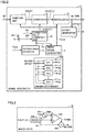
- FIG. 2 is a block diagram showing an internal configuration of signal generator 4 of the power controller according to Embodiment 1.
- Signal generator 4 includes a timing signal generator 8, a sampling unit 7, a corrector 9, a modulator 10, an offset generator 11, an overvoltage detector 12, a correction value operation unit 13, and a driving determiner 410.
- Timing signal generator 8 outputs a timing signal Tsmpl.
- Sampling unit 7 samples shunt command value SP of FIG. 1 in cycles of timing signal Tsmpl, thereby generating a shunt amount NDUTY, which is an amount of operation for adjusting electric power supplied to load 5.
- Corrector 9 corrects shunt amount NDUTY and outputs a corrected shunt amount NDUTY_C.
- Modulator 10 outputs a switch-on count MLPWM based on the corrected shunt amount NDUTY_C.
- modulator 10 When the corrected shunt amount NDUTY_C is an integral value, modulator 10 outputs the integral value as switch-on count MLPWM.
- modulator 10 When the corrected shunt amount NDUTY_C is not an integral value, modulator 10 outputs the sum of an integral part Int and FPWM, which will be described below, as switch-on count MLPWM.
- FIG. 3 shows an example internal configuration of modulator 10 of Embodiment 1.
- Modulator 10 includes a carrier wave generator 401, a divider 406, a comparator 403, and an adder 405.
- Carrier wave generator 401 outputs a carrier wave cw1.
- Divider 406 divides the corrected shunt amount NDUTY_C output from corrector 9 into integral part Int and a fractional part Frac. Since the effective range of shunt amount NDUTY_C is 0 to n, integral part Int is an integral value of 0 to n, and fractional part Frac is a fractional value not less than 0 and less than 1.
- Comparator 403 compares fractional part Frac with carrier wave cw1, thereby generating a fractional part PWM (Pulse Width Modulation) signal FPWM.
- Fractional part PWM signal FPWM assumes a value of 0 or 1 at any appropriate duty ratio.
- An average of fractional part PWM signal FPWM is fractional part Frac.
- Adder 405 adds integral part Int and fractional part PWM signal FPWM (0 or 1) together, thereby calculating switch-on count MLPWM.
- the calculated switch-on count MLPWM is sent to driving determiner 410 of FIG. 2 and is also sent to offset generator 11.
- offset generator 11 converts switch-on count MLPWM into an offset value OFFSET. Offset value OFFSET is sent to driving determiner 410.
- offset generator 11 Upon detection of a decrease in switch-on count MLPWM, offset generator 11 performs modulo addition of an amount of the decrease and offset value OFFSET modulo n, thereby updating offset value OFFSET.
- Offset value OFFSET is a value indicating a starting point of switch elements to be driven and assumes an integral value of 0 to (n-1).
- Switch element S1 is a starting point when offset value OFFSET is 0, and switch element S2 is a starting point when offset value OFFSET is 1.
- the determined switch-on count MLPWM and offset value OFFSET fix the number of switch elements to be turned on among switch elements S1 to Sn and a starting point of the switch elements to be turned, the driving state (on/off) of switch elements S1 to Sn can be determined uniquely.
- Driving determiner 410 includes determiners 411-1 to 411-n.
- switch element Si with a shunt number i can be driven when any of Inequalities (3) and (4) composed of shun number i, shunt stage count n, switch-on count MLPWM, and offset value OFFSET is satisfied.
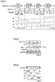
- FIG. 4 is a timing chart showing time changes of shunt amount NDUTY_C, switch-on count MLPWM, and the states of switch elements S1 to S4.
- FIG. 5 is a timing chart showing time changes of shunt amount NDUTY_C, integral part Int, carrier wave cw1 , fractional part PWM signal FPWM, and switch-on count MLPWM.
- FIG. 6 is a timing chart showing time changes of offset value OFFSET and the states of switch elements S1 to S4.
- the horizontal axis represents a lapse of time
- the vertical line represents the state of each signal.
- Illustrated here is an example operation when 2.4 and 1.6 are provided as the corrected shunt amount NDUTY_C.
- switch-on count MLPWM 3 in 40 % of control cycle T
- switch-on count MLPWM 2 in 60 % of control cycle T.
- An average of switch-on counts MLPWM in the first and second control cycles is 2.4.
- Switch-on count MLPWM is 3 at an initial timing of the first control cycle. As a result, three switch elements S1, S2, and S3 are turned on starting from switch element S1.
- Switch-on count MLPWM decreases to 2 at a subsequent timing of the first control cycle.
- two switch elements are turned on starting from switch element S2 while rotating switch elements to be driven. Specifically, switch elements S2 and S3 are turned on.
- switch-on count MLPWM increases to 3, and accordingly, three switch elements are turned on while keeping switch element S2 as the starting point, without rotation. Specifically, switch elements S2, S3, and S4 are turned on.
- switch-on count MLPWM decreases to 2 at a subsequent timing of the second control cycle.
- two switch elements are turned on starting from switch element S3. Specifically, switch elements S3 and S4 are turned on.
- 1.6 is input as a shunt command value.
- switch-on count MLPWM 2 in 60 % of control cycle T
- switch-on count MLPWM 1 in 40 % of control cycle T.
- An average of switch-on counts MLPWM in the third and fourth control cycles is 1.4.
- switch-on count MLPWM is 2 continues at an initial timing of the third control cycle.
- switch elements S3 and S4 are turned on and switch elements S1 and S2 are turned off continues.
- Switch-on count MLPWM decreases to 1 at a subsequent timing of the third control cycle.
- one switch element is turned on starting from switch element S while rotating switch elements to be driven. Specifically, switch element S4 is turned on.
- switch-on count MLPWM increases to 2, and accordingly, two switch elements are turned on while keeping switch element S4 as the starting point, without rotation. Specifically, switch elements S4 and S1 are turned on.
- Switch-on count MLPWM decreases to 1 at a subsequent timing of the fourth control cycle.
- one switch element is turned on starting from switch element S0 while rotating a switch element to be driven. Specifically, switch element S1 is turned on.
- the switching operation can be distributed to all of switch elements S1 to S4, as described above. Accordingly, a timing of switching one switch element can be reduced to one time in four control cycles 4T.
- a switch element which is a starting point is rotated as the switch-on count decreases as described above, and thus, a switch element with the longest on-time among a plurality of turned-on switch elements is turned off.
- switch elements for an amount of switch-on count are turned on from a switch element which is a starting point as the switch-on count increases, and thus, a switch element with the longest off-time among a plurality of turned-off switch elements is turned on.
- the case where the switch-on count decreases by one is described here, which shows a configuration in which a switch element serving as a starting point is rotated by one.
- a rotation may be performed correspondingly.
- the cycle of timing signal Tsmpl is set to reduce heat generation through switching of switch elements S1 to Sn in a stationary operation.
- a bus voltage control operation is performed accompanied by PID control in cycles of timing signal Tsmpl, and accordingly, a negative feedback voltage control operation is updated for each certain switching cycle.
- bus voltage Vbus cannot be controlled for more rapid load fluctuations than the switching cycle, and accordingly, the bus voltage may transiently fluctuate.
- Overvoltage detector 12 is provided as a measure taken when bus voltage Vbus fluctuates greatly due to sudden fluctuations of load 5.
- timing signal generator 8 When a fluctuation range of bus voltage Vbus, which is a voltage supplied to load 5, exceeds a preset fluctuation range due to fluctuations of load 5, overvoltage detector 12 outputs overvoltage detection signal Trn to timing signal generator 8. Upon receipt of overvoltage detection signal Trn, timing signal generator 8 enters a transient response state, thus reducing the cycle of timing signal Tsmpl. This leads to a more rapid bus voltage control response, thus preventing transient occurrence of large fluctuations of bus voltage.
- timing signal generator 8 waits for a time that elapses before heat generation of switch elements S1 to Sn is less affected. Timing signal generator 8 then returns the cycle of timing signal Tsmpl to the cycle in the original stationary operation. This reduces the cycle of timing signal Tsmpl by a period of the transient response state, thus preventing heat generation of switch elements S1 to Sn from being affected.
- bus voltage Vbus may fluctuate again.
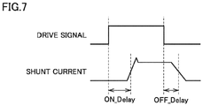
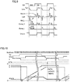
- FIG. 7 shows waveforms of a shunt drive signal and a shunt current.
- a shunt current actually flowing through switch elements S1 to Sn may delay with respect to rising and falling of shunt drive signals of switch elements S1 to Sn.
- a delay time ON_Delay in turn-on may be different from a delay time OFF_Delay in turn-off.
- ON_Duty which is a ratio of an on-time to a switching cycle
- effective ON_Duty which is a ratio of an on-time to a switching cycle of an effective shunt current
- Correction value operation unit 13 performs a correction operation on a difference between effective ON_Duty, which changes dependent on the cycle of timing signal Tsmpl, and ON_Duty of a shunt drive signal, using a value regarded as correction value ⁇ NDUTY in advance regardless of a bus voltage control response operation. This can prevent a phenomenon in which bus voltage Vbus fluctuates again at a timing at which timing signal Tsmpl returns to an original cycle after fluctuations of bus voltage Vbus converge.
- a difference ⁇ Pw of an on-pulse width between a shunt current and a shunt drive signal is expressed by Equation (5).
- the difference ⁇ Pw is a difference between an on-pulse width of a shunt current and an on-pulse width of a shunt drive signal.
- ⁇ Pw ON _ Delay ⁇ OFF _ Delay
- Correction value ⁇ NDUTY which is an amount of change of shunt amount NDUTY caused by a difference ⁇ Pw of the on-pulse width, is expressed by Equation (6) where the cycle of timing signal Tsmpl is T.
- ⁇ NDUTY n ⁇ ⁇ Pw / T
- Correction value operation unit 13 calculates correction value ⁇ NDUTY in accordance with Equations (5) and (6).
- a difference ⁇ Pw of on-pulse width expressed by Equation (5) is a value dependent on the characteristics of switch elements S1 to Sn and a design condition of a shunt driving unit.
- a value of difference ⁇ Pw of on-pulse width thus may be a numeric value determined in design of an apparatus or a numeric value measured in release testing. It is conceivable that difference ⁇ Pw of on-pulse width may fluctuate though it fluctuates by a small amount. Such fluctuations result from temperature fluctuations, a change over the years, or the like, resulting in gradual fluctuations.
- correction value operation unit 13 periodically measures difference ⁇ Pw of on-pulse width, and calculates correction value ⁇ NDUTY for each cycle T of timing signal Tsmpl in accordance with Equation (6).
- Corrector 9 corrects shunt amount NDUTY to nDUTY_C in accordance with Equation (7).
- NDUTY _ C NDUTY ⁇ ⁇ NDUTY
- Equations (5) and (6) may be performed based on a representative shunt drive signal Gn and a differential detection signal Diff of shunt current Ishn to calculate correction value ⁇ NDUTY.
- Shunt drive signal Gn is a signal for driving switch element Sn.
- Shunt current Ishn is a current flowing through switch element Sn.
- Differential detection signal Diff is obtained from, for example, simple current detector 14 including a current transformer or the like.
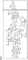
- FIG. 8 is a block diagram showing example configurations of correction value operation unit 13 and corrector 9.
- FIGS. 9 and 10 are timing charts showing signals transmitted in correction value operation unit 13 and corrector 9.
- a comparator CmpH compares differential detection signal Diff that has a differentiated waveform, detected from shunt current Ishn, with a reference value Ref H, and outputs a result of the comparison as an on-timing signal Comp_H of shunt current Ishn.
- Comparator CmpL compares differential detection signal Diff that has a differentiated waveform, detected from shunt current Ishn, with a reference value Ref_L and outputs a result of the comparison as an off-timing signal Comp_L of shunt current Ishn.
- a JK flip-flop JK includes a J input terminal that receives on-timing signal Comp_H of shunt current Ishn and a K input terminal that receives off-timing signal Comp_L of shunt current Ishn and generates a shunt current synchronization signal Ishunt.
- a counter CT1 receives shunt drive signal Gn corresponding to shunt current Ishn and counts a pulse number of clock signal Sysclock during an ON period of shunt drive signal Gn.
- a flip-flop FF1 holds an output from counter CT1 in response to shunt drive signal Gn to output a count value a during the ON period of shunt drive signal Gn.
- a counter CT2 receives shunt current synchronization signal Ishunt corresponding to shunt current Ishn and counts a pulse number of clock signal Sysclock during the ON period of shunt current synchronization signal Ishunt.
- a flip-flop FF2 holds an output from counter CT2 in response to shunt current synchronization signal Ishunt to output a count value b during an ON period of shunt current synchronization signal Ishunt.
- a subtractor Sub1 subtracts count value b during the ON period of shunt current synchronization signal Ishunt from count value a during the ON period of shunt drive signal Gn and outputs a difference d.
- Counter CT1 and counter CT2 each include a zero-load input L and perform a count operation during the ON periods of shunt drive signal Gn and shunt current synchronization signal Ishunt, accompanied by NAND circuits ND1 and ND2.
- a NOR circuit NOR outputs a timing signal c indicating a period in which both of shunt drive signal Gn and shunt current synchronization signal Ishunt are OFF when overvoltage detection signal Trn is not output, that is, during the stationary operation.
- a flip-flop FF3 holds a difference d between the count values in accordance with timing signal c to generate a difference ⁇ Pw of the on-pulse width. Specifically, difference ⁇ Pw of the on-pulse width due to difference d of the count value is generated during a period in which both of shunt drive signal Gn and shunt current synchronization signal Ishunt are OFF in the state where overvoltage detection signal Trn is not output, that is, during the stationary operation.
- a selector SL selects a coefficient C_trn or C_Norm in accordance with whether it is a time at which overvoltage detection signal Trn is output.
- Coefficient C_trn is a coefficient corresponding to the time at which overvoltage detection signal Trn is output.
- Coefficient C_Norm is a coefficient corresponding to a time at which overvoltage detection signal Trn is not output.
- Coefficient C_trn and coefficient C_Norm are expressed by Equations (8) and (9), respectively, from Equations (6) using a total number n of switch elements S1 to Sn.
- C _ trn n / Ttrn
- C _ Norm n / Tnrm
- Ttrn in Equation (8) represents a cycle of timing signal Tsmpl when overvoltage detection signal Trn is output, that is, in the transient response state.
- Tnrm in Equation (9) represents a cycle of timing signal Tsmpl when overvoltage detection signal Trn is not output, that is, in the stationary operation. The following is satisfied. Specifically, the length of the control cycle in the transient response state is shorter than the length of the control cycle in the stationary operation. Ttrn ⁇ Tnrm
- a multiplier Mull multiplies difference ⁇ Pw of the on-pulse width by an output from selector SL, thereby generating a correction value ⁇ NDUTY.
- a subtractor Sub2 generates a shunt amount NDUTY_C obtained by correction through subtraction of correction value ⁇ NDUTY from shunt amount NDUTY.
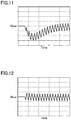
- FIG. 11 shows a simulation result of a waveform of bus voltage Vbus when pulse width correction control is not performed.
- FIG. 12 shows a simulation result of the waveform of bus voltage Vbus when pulse width correction control is performed.
- the simulation result is obtained by simulating fluctuations of bus voltage Vbus when the state in which the cycle of timing signal Tsmpl is shorter in the transient response state is returned to the state in which the normal cycle of timing signal Tsmpl.
- the cycle of timing signal Tsmpl is switched in the vicinity of 15 % of the horizontal axis. It is found that when pulse width correction control is not performed, bus voltage Vbus decreases due to fluctuations of effective ON_Duty. When pulse width correction control described in Embodiment 1 is performed, effective ON Duty can be kept constant, thus reducing fluctuations of bus voltage Vbus.
- the power controller that performs control with a constant bus voltage obtains a shunt command value, which is an average of the numbers for shunt, from a deviation between a bus voltage and a target value, and rotates a switch element to be driven, at a timing at which the switch-on count increases or decreases while controlling a switch-on count of switch elements and a duty ratio, as described above.
- the present Embodiment can thus reduce heat generation associated with switching while maintaining the stability of a bus voltage.
- the present Embodiment can thus relax the condition for selecting components and heat dissipation design. Consequently, a power controller can be provided that has a high response, a smaller size, a smaller weight, and an excellent electrical power quality.
- Power controller 1 of a variation of Embodiment 1 is obtained by modifying the internal configurations of modulator 10 and driving determiner 410 in power controller 1 of Embodiment 1.
- the other configuration of the power controller of the variation of Embodiment 1 is similar to that of FIG. 1 , which will not be described repeatedly.
- FIG. 13 shows examples of modulator 10 and driving determiner 410 of the variation of Embodiment 1. The case where shunt stage count n is 4 will be described here for ease of explanation.
- Modulator 10 includes carrier wave generator 401, offset superimposing units 402-1 to 402-3, comparators 403-1 to 403-4, and an adder 405.
- Driving determiner 410 includes an offset generator 11 and a drive signal assignment unit 409.
- FIGS. 14 and 15 are timing charts showing the waveforms of signals transmitted in modulator 10 and driving determiner 410 of FIG. 13 .
- Carrier wave generator 401 generates a carrier wave cw1 having an amplitude of 1 and sends carrier wave cw1 to comparator 403-1 and offset superimposing unit 402-1.
- Offset superimposing unit 402-1 sends, to offset superimposing unit 402-2 and comparator 403-2, a signal cw2 obtained by adding an offset equal to the amplitude of carrier wave cw1 to carrier wave cw1.
- Offset superimposing unit 402-2 sends, to offset superimposing unit 402-3 and comparator 403-3, a signal cw3 obtained by adding an offset equal to the amplitude of carrier wave cw1 to signal cw2.
- Offset superimposing unit 402-3 sends, to comparator 403-4, a signal cw4 obtained by adding an offset equal to the amplitude of carrier wave cw1 to signal cw3.
- Comparator 403-i 1 to 4) compares the corrected shunt amount NDUTY_C with carrier wave cwi and outputs a PWM signal Pi. When shunt amount NDUTY_C is greater than carrier wave cwi, PWM signal Pi is "1". When shunt amount NDUTY_C is not greater than carrier wave cwi, PWM signal Pi is "0". An output from comparator 403 with the number corresponding to the switch-on count MLPWM is "1".
- This operation yields a PWM signal obtained by dividing a signal domain by the shunt stage count.
- Adder 405 adds PWM signals P1 to P4, which are outputs from comparators 403-1 to 403-4, together and outputs switch-on count MLPWM.
- Offset generator 11 assigns offset value OFFSET based on switch-on count MLPWM as in Embodiment 1.
- PWM signal determined so far and offset value OFFSET fix a drive pattern of switch elements and a starting point thereof, and accordingly, the drive state (on/off) of each switch element can be determined uniquely.
- Drive signal assignment unit 409 performs a cyclic shift operation on PWM signal Pi output from comparator 403-i by offset value OFFSET to drive each switch element to be turned on or off.
- FIG. 13 shows an example in which two-input, one-output multiplexers are combined for cyclic shift, a multi-input multiplexer may be used for cyclic shift.
- Power controller 1 of Embodiment 2 is obtained by modifying the internal configuration of signal generator 4 in power controller 1 of Embodiment 1.
- the other configuration of the power controller according to Embodiment 2 is similar to that of FIG. 1 , which will not be described repeatedly.
- FIG. 16 is a block diagram showing an internal configuration of signal generator 4 of power controller 1 of Embodiment 2.
- Signal generator 4 includes a comparator 17, a counter 16, offset generator 11, and driving determiner 410. Offset generator 11 and driving determiner 410 are similar to those of Embodiment 1, which will not be described repeatedly.
- Comparator 17 compares first to n-th on-level thresholds, which are assigned within a variable range of shunt command value SP, and first to n-th off-level thresholds, which are assigned to have a hysteresis corresponding one-to-one to the first to n-th on-level thresholds, with shunt command value SP.
- Counter 16 determines switch-on count MLPWM based on a result of the comparison of comparator 17.
- the JK flip-flops may be replaced by RS flip-flops.
- An i-th on-comparator Hii compares shunt command value SP with an i-th on-level threshold ONi.
- the i-th on-comparator Hii outputs "1" when shunt command value SP is greater than the i-th on-level threshold ONi and outputs "0" when shunt command value SP is smaller than the i-th on-level threshold ONi.
- the i-th on-comparator Hii sends a result of the comparison to a J input terminal of JK flip-flop FFdi of counter 16.
- An i-th off-comparator Loi compares shunt command value SP with an i-th off-level threshold OFFi.
- the i-th off-comparator Loi outputs "1" when the i-th off-level threshold OFFi is greater than shunt command value SP and outputs "0" when the i-th off-level threshold OFFi is smaller than shunt command value SP.
- the i-th off-comparator Loi sends a result of the comparison to a K input terminal of JK flip-flop FFdi of counter 16.
- An i-th JK flip-flop FFdi includes a J input terminal that receives an output from the i-th on-comparator Hii and a K input terminal that receives an output from the i-th off-comparator Loi.
- Adder 15 adds outputs x1 to xn of JK flip-flops FFd1 to FFdn together and sends an addition value as switch-on count MLPWM to driving determiner 410 and offset generator 11.
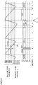
- FIG. 17 is a timing chart showing time changes of shunt command value SP, outputs x1 to xn of JK flip-flops FFd1 to FFdn, and switch-on count MLPWM.
- FIG. 17 also shows on-level thresholds ON1 to ONn and off-level thresholds OFF1 to OFFn.
- the number of stages n of DC power supplies I1 to In is 5 for ease of explanation.
- shunt command value SP is expressed by Equation (13) as a signal indicating an error from target control value Vref in relation to bus voltage Vbus.
- SP Vbus ⁇ Vref ⁇ A
- Equation (12) A is a value indicating an amplification degree of operation processing unit 3A and is set as an amplification degree with appropriate frequency characteristics, and A is 1 here for ease of explanation. This is because the relation between on-level thresholds ON1 to ON5 and off-level thresholds OFF1 to OFF5, and shunt command value SP is normalized for description.
- switch elements S1, S2 are opened (off state) when shunt command value SP falls below off-level thresholds OFF1, OFF2.
- Switch elements S2 to S5 are shunted (on state) when shunt command value SP exceeds on-level thresholds ON2 to ON5.
- on-level thresholds ON1 to ONn and off-level thresholds OFF1 to OFFn are set as thresholds with hystereses that determine on and off of switch elements S1 to Sn relative to shunt command value SP.
- the setting range of on-level thresholds ON1 to ONn or the setting range of off-level thresholds OFF1 to OFFn is a control voltage fluctuation range ⁇ Vbus of bus voltage Vbus.
- bus voltage Vbus fluctuates dependent on a solar battery generation current Istr per stage, bus capacitor Cbus, and load current Iload.
- a time change ratio of bus voltage Vbusdv/dt is expressed by Equation (14).
- dV / dt Istr ⁇ n ⁇ MLPWM ⁇ Iload / Cbus
- the value of switch-on count MLPWM changes every time shunt command value SP crosses on-level thresholds ON1 to ONn and off-level thresholds OFF1 to OFFn.
- Power controller 1 controls a bus voltage such that bus voltage Vbus falls within the range of a defined control voltage fluctuation range ⁇ Vbus, accompanied by ripple voltage Vripple, while dissipating heat generated through switching of switch elements S1 to Sn.
- Equation 15 A minimum cycle Tmin in the state in which the switching cycle continues steadily is expressed by Equation (15).
- Tmin 4 ⁇ Cbus ⁇ Vripple / Istr According to Equation (15), thus, minimum cycle Tmin that can be continued steadily can be set within an allowable range of heat generation of switch elements S1 to Sn by selecting a related constant and designing power controller 1.
- the above principle stabilizes a bus voltage relative to rapid load fluctuations without increasing heat generation by switching of each switch element during steady operation.
- the comparator compares as many on-level thresholds and off-level thresholds as the shunt stage count, each of which has a hysteresis relative to a fluctuation range of a bus voltage, with the bus voltage, the flip-flop latches a result of the comparison, and the counter adds up the comparison results, thereby calculating a switch-on count MLPWM.
- the switching cycle is restricted to an appropriate range, and heat generation by switching of a switch element does not increase.
- switching intervals are shorter, and a control response can be made also to rapid load fluctuations, thus preventing transient occurrence of large bus voltage fluctuations. Consequently, a power controller with an excellent power quality can be provided without hindering a power controller from having a smaller size and a lighter weight.
- the present variation relates to a case where signal generator 4 is configured by an integrated circuit or software.
- FIG. 18 is a block diagram showing a part of an internal configuration of signal generator 4 of power controller 1 according to the variation of Embodiment 2.
- Signal generator 4 includes an adder 551, a subtractor 552, a multiplier 553, a multiplier 555, an integer formatting unit 554, an integer formatting unit 556, a comparator 557, a comparator 558, and a counter 559.
- Adder 551 adds shunt command value SP and Vrippe/2 together.
- Subtractor 552 subtracts Vrippe/2 from shunt command value SP.
- Multiplier 553 multiplies an output from adder 551 by n/ ⁇ Vbus.
- Multiplier 555 multiples an output from subtractor 552 by n/ ⁇ Vbus.
- Integer formatting unit 554 outputs an integral part of an output from multiplier 553.
- Integer formatting unit 556 outputs an integral part of an output from multiplier 555.
- Comparator 557 compares an output from integer formatting unit 554 with switch-on count MLPWM. Comparator 557 outputs "1" when the output from integer formatting unit 554 is greater than switch-on count MLPWM. Comparator 557 outputs "0" when the output from integer formatting unit 554 is smaller than switch-on count MLPWM.
- Comparator 558 compares an output from integer formatting unit 556 with switch-on count MLPWM. Comparator 558 outputs "0" when the output from integer formatting unit 556 is greater than switch-on count MLPWM. Comparator 558 outputs "1" when the output from integer formatting unit 554 is smaller than switch-on count MLPWM.
- Counter 559 increments a count value by an output from comparator 557 and decrements the count value by an output from comparator 558. Counter 559 outputs switch-on count MLPWM as the count value.
- the present variation can replace the above operation in which thresholds and comparators required for the shunt stage count with an operation in which thresholds and comparators are not dependent on the stage count, leading to a simplified operation.
- the present invention is not limited to the above embodiments and includes, for example, the following variations.
Landscapes
- Engineering & Computer Science (AREA)
- Power Engineering (AREA)
- Physics & Mathematics (AREA)
- Nonlinear Science (AREA)
- Dc-Dc Converters (AREA)
- Control Of Voltage And Current In General (AREA)
Applications Claiming Priority (1)
| Application Number | Priority Date | Filing Date | Title |
|---|---|---|---|
| PCT/JP2019/003283 WO2020157884A1 (ja) | 2019-01-31 | 2019-01-31 | 電力制御器 |
Publications (3)
| Publication Number | Publication Date |
|---|---|
| EP3920004A1 true EP3920004A1 (de) | 2021-12-08 |
| EP3920004A4 EP3920004A4 (de) | 2022-01-19 |
| EP3920004B1 EP3920004B1 (de) | 2025-08-27 |
Family
ID=70057993
Family Applications (1)
| Application Number | Title | Priority Date | Filing Date |
|---|---|---|---|
| EP19912707.7A Active EP3920004B1 (de) | 2019-01-31 | 2019-01-31 | Leistungsregler |
Country Status (4)
| Country | Link |
|---|---|
| US (1) | US11387816B2 (de) |
| EP (1) | EP3920004B1 (de) |
| JP (1) | JP6678826B1 (de) |
| WO (1) | WO2020157884A1 (de) |
Families Citing this family (1)
| Publication number | Priority date | Publication date | Assignee | Title |
|---|---|---|---|---|
| JP7614136B2 (ja) | 2022-04-18 | 2025-01-15 | 三菱電機株式会社 | 電力制御器 |
Family Cites Families (10)
| Publication number | Priority date | Publication date | Assignee | Title |
|---|---|---|---|---|
| US4706010A (en) * | 1986-09-10 | 1987-11-10 | Rca Corporation | Linear solar array voltage control system |
| US5814903A (en) * | 1996-09-13 | 1998-09-29 | Lockheed Martin Corporation | Programmable gain for switched power control |
| FR2785103B1 (fr) * | 1998-10-23 | 2000-12-22 | Agence Spatiale Europeenne | Dispositif de generation d'energie electrique pour bus d'alimentation |
| JP4387729B2 (ja) * | 2003-08-27 | 2009-12-24 | Nec東芝スペースシステム株式会社 | 電源シャント装置及び電源システムの電圧制御方法 |
| JP5102080B2 (ja) * | 2008-03-17 | 2012-12-19 | 日立オートモティブシステムズ株式会社 | 車両用モータの制御装置 |
| JP5423306B2 (ja) * | 2009-10-14 | 2014-02-19 | 三菱電機株式会社 | 電力制御器 |
| JP2013255399A (ja) * | 2012-06-08 | 2013-12-19 | Auto Network Gijutsu Kenkyusho:Kk | 車両用電源制御装置 |
| JP5987609B2 (ja) | 2012-09-28 | 2016-09-07 | 三菱電機株式会社 | 電力制御器 |
| JP6119560B2 (ja) * | 2013-10-31 | 2017-04-26 | 三菱電機株式会社 | 電力制御器 |
| WO2017145362A1 (ja) * | 2016-02-26 | 2017-08-31 | 三菱電機株式会社 | 電力制御器 |
-
2019
- 2019-01-31 WO PCT/JP2019/003283 patent/WO2020157884A1/ja not_active Ceased
- 2019-01-31 US US17/417,115 patent/US11387816B2/en active Active
- 2019-01-31 JP JP2019528928A patent/JP6678826B1/ja active Active
- 2019-01-31 EP EP19912707.7A patent/EP3920004B1/de active Active
Also Published As
| Publication number | Publication date |
|---|---|
| EP3920004B1 (de) | 2025-08-27 |
| JPWO2020157884A1 (ja) | 2021-02-18 |
| EP3920004A4 (de) | 2022-01-19 |
| JP6678826B1 (ja) | 2020-04-08 |
| WO2020157884A1 (ja) | 2020-08-06 |
| US20220077846A1 (en) | 2022-03-10 |
| US11387816B2 (en) | 2022-07-12 |
Similar Documents
| Publication | Publication Date | Title |
|---|---|---|
| US10263524B2 (en) | Multi-phase parallel converter and controlling method therefor | |
| US9225191B2 (en) | Circuit and method for voltage equalization in large batteries | |
| US10651721B2 (en) | Multi-phase converter and associated control circuit and control method for undershoot improvement | |
| US9287777B2 (en) | Average current controller, average current control method and buck converter using the average current controller | |
| KR20230085195A (ko) | 광발전 시스템의 버스바 전압 제어 방법 및 장치 | |
| US20170222557A1 (en) | Load capacitance determination circuitry and power supply control | |
| DK201970833A1 (en) | Controlling on-time of energy modules of an energy storage | |
| WO2020256690A1 (en) | Voltage balance systems and methods for multilevel converters | |
| US10491018B2 (en) | Power output management apparatus of battery and managment method thereof | |
| US11177730B2 (en) | On-time compensation in a power converter | |
| EP3421379B1 (de) | Stromsteuerungsvorrichtung | |
| US11635780B2 (en) | Maximum power point tracking apparatus for energy harvesting system and maximum power point tracking control method | |
| CN101656419A (zh) | 固定工作时间控制的多相电源转换器的电流平衡装置及方法 | |
| JP2016067168A (ja) | マトリクスコンバータ、発電システムおよび電力変換方法 | |
| EP3920004B1 (de) | Leistungsregler | |
| JPWO2011093269A1 (ja) | 電力変換装置 | |
| US9647546B2 (en) | Dual-mode voltage doubling buck converter with smooth mode transition | |
| US20200136514A1 (en) | System and Method for Balancing Current of Converter Phases | |
| KR101572612B1 (ko) | 배터리용 순환전류 제어 장치 | |
| US20180367134A1 (en) | Voltage balancing of voltage source converters | |
| EP3723256B1 (de) | Ausgangsspannungssteuerungsschaltung für mehrere in reihe geschaltete stromversorgungszellen | |
| JP5987609B2 (ja) | 電力制御器 | |
| KR20210155104A (ko) | 스위칭 손실이 개선된 dpwm 방식을 적용한 3상 4레그 인버터의 스위칭 함수 발생 방법 및 스위칭 함수 발생기. | |
| RU2806896C1 (ru) | Повышающий регулятор напряжения для работы с трёхфазной нагрузкой | |
| JP2015089242A (ja) | 電力制御器 |
Legal Events
| Date | Code | Title | Description |
|---|---|---|---|
| STAA | Information on the status of an ep patent application or granted ep patent |
Free format text: STATUS: THE INTERNATIONAL PUBLICATION HAS BEEN MADE |
|
| PUAI | Public reference made under article 153(3) epc to a published international application that has entered the european phase |
Free format text: ORIGINAL CODE: 0009012 |
|
| STAA | Information on the status of an ep patent application or granted ep patent |
Free format text: STATUS: REQUEST FOR EXAMINATION WAS MADE |
|
| 17P | Request for examination filed |
Effective date: 20210723 |
|
| AK | Designated contracting states |
Kind code of ref document: A1 Designated state(s): AL AT BE BG CH CY CZ DE DK EE ES FI FR GB GR HR HU IE IS IT LI LT LU LV MC MK MT NL NO PL PT RO RS SE SI SK SM TR |
|
| REG | Reference to a national code |
Ref country code: DE Ref legal event code: R079 Free format text: PREVIOUS MAIN CLASS: G05F0001000000 Ipc: H02J0001100000 Ref country code: DE Ref legal event code: R079 Ref document number: 602019074972 Country of ref document: DE Free format text: PREVIOUS MAIN CLASS: G05F0001000000 Ipc: H02J0001100000 |
|
| A4 | Supplementary search report drawn up and despatched |
Effective date: 20211222 |
|
| RIC1 | Information provided on ipc code assigned before grant |
Ipc: H02M 1/00 20060101ALI20211216BHEP Ipc: H02J 1/10 20060101AFI20211216BHEP |
|
| DAV | Request for validation of the european patent (deleted) | ||
| DAX | Request for extension of the european patent (deleted) | ||
| RIC1 | Information provided on ipc code assigned before grant |
Ipc: H02M 1/00 20060101ALI20240918BHEP Ipc: H02J 1/10 20060101AFI20240918BHEP |
|
| GRAP | Despatch of communication of intention to grant a patent |
Free format text: ORIGINAL CODE: EPIDOSNIGR1 |
|
| STAA | Information on the status of an ep patent application or granted ep patent |
Free format text: STATUS: GRANT OF PATENT IS INTENDED |
|
| INTG | Intention to grant announced |
Effective date: 20241029 |
|
| GRAJ | Information related to disapproval of communication of intention to grant by the applicant or resumption of examination proceedings by the epo deleted |
Free format text: ORIGINAL CODE: EPIDOSDIGR1 |
|
| STAA | Information on the status of an ep patent application or granted ep patent |
Free format text: STATUS: REQUEST FOR EXAMINATION WAS MADE |
|
| GRAP | Despatch of communication of intention to grant a patent |
Free format text: ORIGINAL CODE: EPIDOSNIGR1 |
|
| STAA | Information on the status of an ep patent application or granted ep patent |
Free format text: STATUS: GRANT OF PATENT IS INTENDED |
|
| INTC | Intention to grant announced (deleted) | ||
| INTG | Intention to grant announced |
Effective date: 20250324 |
|
| GRAS | Grant fee paid |
Free format text: ORIGINAL CODE: EPIDOSNIGR3 |
|
| GRAA | (expected) grant |
Free format text: ORIGINAL CODE: 0009210 |
|
| STAA | Information on the status of an ep patent application or granted ep patent |
Free format text: STATUS: THE PATENT HAS BEEN GRANTED |
|
| AK | Designated contracting states |
Kind code of ref document: B1 Designated state(s): AL AT BE BG CH CY CZ DE DK EE ES FI FR GB GR HR HU IE IS IT LI LT LU LV MC MK MT NL NO PL PT RO RS SE SI SK SM TR |
|
| REG | Reference to a national code |
Ref country code: GB Ref legal event code: FG4D |
|
| REG | Reference to a national code |
Ref country code: CH Ref legal event code: EP |
|
| REG | Reference to a national code |
Ref country code: DE Ref legal event code: R096 Ref document number: 602019074972 Country of ref document: DE |
|
| REG | Reference to a national code |
Ref country code: IE Ref legal event code: FG4D |
|
| REG | Reference to a national code |
Ref country code: NL Ref legal event code: MP Effective date: 20250827 |
|
| PG25 | Lapsed in a contracting state [announced via postgrant information from national office to epo] |
Ref country code: IS Free format text: LAPSE BECAUSE OF FAILURE TO SUBMIT A TRANSLATION OF THE DESCRIPTION OR TO PAY THE FEE WITHIN THE PRESCRIBED TIME-LIMIT Effective date: 20251227 |
|
| PG25 | Lapsed in a contracting state [announced via postgrant information from national office to epo] |
Ref country code: NO Free format text: LAPSE BECAUSE OF FAILURE TO SUBMIT A TRANSLATION OF THE DESCRIPTION OR TO PAY THE FEE WITHIN THE PRESCRIBED TIME-LIMIT Effective date: 20251127 |
|
| REG | Reference to a national code |
Ref country code: LT Ref legal event code: MG9D |
|
| PG25 | Lapsed in a contracting state [announced via postgrant information from national office to epo] |
Ref country code: PT Free format text: LAPSE BECAUSE OF FAILURE TO SUBMIT A TRANSLATION OF THE DESCRIPTION OR TO PAY THE FEE WITHIN THE PRESCRIBED TIME-LIMIT Effective date: 20251229 |
|
| PG25 | Lapsed in a contracting state [announced via postgrant information from national office to epo] |
Ref country code: FI Free format text: LAPSE BECAUSE OF FAILURE TO SUBMIT A TRANSLATION OF THE DESCRIPTION OR TO PAY THE FEE WITHIN THE PRESCRIBED TIME-LIMIT Effective date: 20250827 |
|
| PG25 | Lapsed in a contracting state [announced via postgrant information from national office to epo] |
Ref country code: NL Free format text: LAPSE BECAUSE OF FAILURE TO SUBMIT A TRANSLATION OF THE DESCRIPTION OR TO PAY THE FEE WITHIN THE PRESCRIBED TIME-LIMIT Effective date: 20250827 Ref country code: HR Free format text: LAPSE BECAUSE OF FAILURE TO SUBMIT A TRANSLATION OF THE DESCRIPTION OR TO PAY THE FEE WITHIN THE PRESCRIBED TIME-LIMIT Effective date: 20250827 |
|
| PGFP | Annual fee paid to national office [announced via postgrant information from national office to epo] |
Ref country code: FR Payment date: 20251128 Year of fee payment: 8 |
|
| PG25 | Lapsed in a contracting state [announced via postgrant information from national office to epo] |
Ref country code: GR Free format text: LAPSE BECAUSE OF FAILURE TO SUBMIT A TRANSLATION OF THE DESCRIPTION OR TO PAY THE FEE WITHIN THE PRESCRIBED TIME-LIMIT Effective date: 20251128 |
|
| PGFP | Annual fee paid to national office [announced via postgrant information from national office to epo] |
Ref country code: BE Payment date: 20251223 Year of fee payment: 8 |
|
| PG25 | Lapsed in a contracting state [announced via postgrant information from national office to epo] |
Ref country code: SE Free format text: LAPSE BECAUSE OF FAILURE TO SUBMIT A TRANSLATION OF THE DESCRIPTION OR TO PAY THE FEE WITHIN THE PRESCRIBED TIME-LIMIT Effective date: 20250827 |
|
| PG25 | Lapsed in a contracting state [announced via postgrant information from national office to epo] |
Ref country code: LV Free format text: LAPSE BECAUSE OF FAILURE TO SUBMIT A TRANSLATION OF THE DESCRIPTION OR TO PAY THE FEE WITHIN THE PRESCRIBED TIME-LIMIT Effective date: 20250827 |
|
| PG25 | Lapsed in a contracting state [announced via postgrant information from national office to epo] |
Ref country code: BG Free format text: LAPSE BECAUSE OF FAILURE TO SUBMIT A TRANSLATION OF THE DESCRIPTION OR TO PAY THE FEE WITHIN THE PRESCRIBED TIME-LIMIT Effective date: 20250827 Ref country code: PL Free format text: LAPSE BECAUSE OF FAILURE TO SUBMIT A TRANSLATION OF THE DESCRIPTION OR TO PAY THE FEE WITHIN THE PRESCRIBED TIME-LIMIT Effective date: 20250827 |
|
| PG25 | Lapsed in a contracting state [announced via postgrant information from national office to epo] |
Ref country code: RS Free format text: LAPSE BECAUSE OF FAILURE TO SUBMIT A TRANSLATION OF THE DESCRIPTION OR TO PAY THE FEE WITHIN THE PRESCRIBED TIME-LIMIT Effective date: 20251127 |
|
| PG25 | Lapsed in a contracting state [announced via postgrant information from national office to epo] |
Ref country code: ES Free format text: LAPSE BECAUSE OF FAILURE TO SUBMIT A TRANSLATION OF THE DESCRIPTION OR TO PAY THE FEE WITHIN THE PRESCRIBED TIME-LIMIT Effective date: 20250827 |