EP3911130A1 - Transfer von viskosen materialien - Google Patents
Transfer von viskosen materialien Download PDFInfo
- Publication number
- EP3911130A1 EP3911130A1 EP20174175.8A EP20174175A EP3911130A1 EP 3911130 A1 EP3911130 A1 EP 3911130A1 EP 20174175 A EP20174175 A EP 20174175A EP 3911130 A1 EP3911130 A1 EP 3911130A1
- Authority
- EP
- European Patent Office
- Prior art keywords
- functional material
- zone
- heater elements
- cavity
- donor area
- Prior art date
- Legal status (The legal status is an assumption and is not a legal conclusion. Google has not performed a legal analysis and makes no representation as to the accuracy of the status listed.)
- Withdrawn
Links
Images


Classifications
-
- H—ELECTRICITY
- H05—ELECTRIC TECHNIQUES NOT OTHERWISE PROVIDED FOR
- H05K—PRINTED CIRCUITS; CASINGS OR CONSTRUCTIONAL DETAILS OF ELECTRIC APPARATUS; MANUFACTURE OF ASSEMBLAGES OF ELECTRICAL COMPONENTS
- H05K3/00—Apparatus or processes for manufacturing printed circuits
- H05K3/10—Apparatus or processes for manufacturing printed circuits in which conductive material is applied to the insulating support in such a manner as to form the desired conductive pattern
- H05K3/12—Apparatus or processes for manufacturing printed circuits in which conductive material is applied to the insulating support in such a manner as to form the desired conductive pattern using thick film techniques, e.g. printing techniques to apply the conductive material or similar techniques for applying conductive paste or ink patterns
- H05K3/1258—Apparatus or processes for manufacturing printed circuits in which conductive material is applied to the insulating support in such a manner as to form the desired conductive pattern using thick film techniques, e.g. printing techniques to apply the conductive material or similar techniques for applying conductive paste or ink patterns by using a substrate provided with a shape pattern, e.g. grooves, banks, resist pattern
-
- H—ELECTRICITY
- H05—ELECTRIC TECHNIQUES NOT OTHERWISE PROVIDED FOR
- H05B—ELECTRIC HEATING; ELECTRIC LIGHT SOURCES NOT OTHERWISE PROVIDED FOR; CIRCUIT ARRANGEMENTS FOR ELECTRIC LIGHT SOURCES, IN GENERAL
- H05B1/00—Details of electric heating devices
- H05B1/02—Automatic switching arrangements specially adapted to apparatus ; Control of heating devices
- H05B1/0227—Applications
- H05B1/023—Industrial applications
- H05B1/0244—Heating of fluids
-
- H—ELECTRICITY
- H05—ELECTRIC TECHNIQUES NOT OTHERWISE PROVIDED FOR
- H05B—ELECTRIC HEATING; ELECTRIC LIGHT SOURCES NOT OTHERWISE PROVIDED FOR; CIRCUIT ARRANGEMENTS FOR ELECTRIC LIGHT SOURCES, IN GENERAL
- H05B3/00—Ohmic-resistance heating
- H05B3/20—Heating elements having extended surface area substantially in a two-dimensional plane, e.g. plate-heater
- H05B3/22—Heating elements having extended surface area substantially in a two-dimensional plane, e.g. plate-heater non-flexible
-
- H—ELECTRICITY
- H05—ELECTRIC TECHNIQUES NOT OTHERWISE PROVIDED FOR
- H05K—PRINTED CIRCUITS; CASINGS OR CONSTRUCTIONAL DETAILS OF ELECTRIC APPARATUS; MANUFACTURE OF ASSEMBLAGES OF ELECTRICAL COMPONENTS
- H05K3/00—Apparatus or processes for manufacturing printed circuits
- H05K3/02—Apparatus or processes for manufacturing printed circuits in which the conductive material is applied to the surface of the insulating support and is thereafter removed from such areas of the surface which are not intended for current conducting or shielding
- H05K3/04—Apparatus or processes for manufacturing printed circuits in which the conductive material is applied to the surface of the insulating support and is thereafter removed from such areas of the surface which are not intended for current conducting or shielding the conductive material being removed mechanically, e.g. by punching
- H05K3/046—Apparatus or processes for manufacturing printed circuits in which the conductive material is applied to the surface of the insulating support and is thereafter removed from such areas of the surface which are not intended for current conducting or shielding the conductive material being removed mechanically, e.g. by punching by selective transfer or selective detachment of a conductive layer
-
- H—ELECTRICITY
- H05—ELECTRIC TECHNIQUES NOT OTHERWISE PROVIDED FOR
- H05B—ELECTRIC HEATING; ELECTRIC LIGHT SOURCES NOT OTHERWISE PROVIDED FOR; CIRCUIT ARRANGEMENTS FOR ELECTRIC LIGHT SOURCES, IN GENERAL
- H05B2203/00—Aspects relating to Ohmic resistive heating covered by group H05B3/00
- H05B2203/002—Heaters using a particular layout for the resistive material or resistive elements
- H05B2203/005—Heaters using a particular layout for the resistive material or resistive elements using multiple resistive elements or resistive zones isolated from each other
-
- H—ELECTRICITY
- H05—ELECTRIC TECHNIQUES NOT OTHERWISE PROVIDED FOR
- H05B—ELECTRIC HEATING; ELECTRIC LIGHT SOURCES NOT OTHERWISE PROVIDED FOR; CIRCUIT ARRANGEMENTS FOR ELECTRIC LIGHT SOURCES, IN GENERAL
- H05B2203/00—Aspects relating to Ohmic resistive heating covered by group H05B3/00
- H05B2203/019—Heaters using heating elements having a negative temperature coefficient
-
- H—ELECTRICITY
- H05—ELECTRIC TECHNIQUES NOT OTHERWISE PROVIDED FOR
- H05K—PRINTED CIRCUITS; CASINGS OR CONSTRUCTIONAL DETAILS OF ELECTRIC APPARATUS; MANUFACTURE OF ASSEMBLAGES OF ELECTRICAL COMPONENTS
- H05K2203/00—Indexing scheme relating to apparatus or processes for manufacturing printed circuits covered by H05K3/00
- H05K2203/01—Tools for processing; Objects used during processing
- H05K2203/0104—Tools for processing; Objects used during processing for patterning or coating
- H05K2203/0113—Female die used for patterning or transferring, e.g. temporary substrate having recessed pattern
-
- H—ELECTRICITY
- H05—ELECTRIC TECHNIQUES NOT OTHERWISE PROVIDED FOR
- H05K—PRINTED CIRCUITS; CASINGS OR CONSTRUCTIONAL DETAILS OF ELECTRIC APPARATUS; MANUFACTURE OF ASSEMBLAGES OF ELECTRICAL COMPONENTS
- H05K2203/00—Indexing scheme relating to apparatus or processes for manufacturing printed circuits covered by H05K3/00
- H05K2203/05—Patterning and lithography; Masks; Details of resist
- H05K2203/0502—Patterning and lithography
- H05K2203/0528—Patterning during transfer, i.e. without preformed pattern, e.g. by using a die, a programmed tool or a laser
-
- H—ELECTRICITY
- H05—ELECTRIC TECHNIQUES NOT OTHERWISE PROVIDED FOR
- H05K—PRINTED CIRCUITS; CASINGS OR CONSTRUCTIONAL DETAILS OF ELECTRIC APPARATUS; MANUFACTURE OF ASSEMBLAGES OF ELECTRICAL COMPONENTS
- H05K2203/00—Indexing scheme relating to apparatus or processes for manufacturing printed circuits covered by H05K3/00
- H05K2203/08—Treatments involving gases
- H05K2203/083—Evaporation or sublimation of a compound, e.g. gas bubble generating agent
-
- H—ELECTRICITY
- H05—ELECTRIC TECHNIQUES NOT OTHERWISE PROVIDED FOR
- H05K—PRINTED CIRCUITS; CASINGS OR CONSTRUCTIONAL DETAILS OF ELECTRIC APPARATUS; MANUFACTURE OF ASSEMBLAGES OF ELECTRICAL COMPONENTS
- H05K2203/00—Indexing scheme relating to apparatus or processes for manufacturing printed circuits covered by H05K3/00
- H05K2203/11—Treatments characterised by their effect, e.g. heating, cooling, roughening
- H05K2203/1105—Heating or thermal processing not related to soldering, firing, curing or laminating, e.g. for shaping the substrate or during finish plating
Definitions
- the invention relates to a method of transferring a high viscosity functional material, such as an electrically conductive or an electrically insulating paste, on a substrate.
- the invention further relates to a device for transferring such a material.
- the invention still further relates to a record carrier comprising instructions that when executed by a programmable processor causes an apparatus to perform the method.
- Interconnection of discrete bare chip components or microelectronic components (chips) on a substrate is a process for which precision material deposition with sufficient accuracy is necessary to allow for miniature electrical or other type of interconnects so that when a chip component becomes attached to a placement position all electrical connection and fixation to the substrate can be made by a conductive material or paste.
- a conductive adhesives is a thermal or UV settable resin loaded with silver particles, or a solder paste comprising solder particles and flux.
- the functional material to be deposited may be a thermal conductor, or instead a thermal insulator.
- Printing is an example of a common method for selectively depositing a functional material on a substrate.
- a functional material needs to be formulated with other materials before the functional material can be printed on a substrate.
- a formulation can e.g. be formed by dispersing the functional material in a solvent or liquid; thus, the formulation is generally wet.
- the formulation is often referred to as an ink or paste, depending on the viscosity.
- Such materials e.g. consist of more than 50 vol% e.g. even 90 vol% of a solid state material such as a conductive polymer.
- the functional materials to be deposited are of a high viscosity, e.g. higher than 50 Pa.s to even as much as about 1000 Pa.s (10 6 cp.s).
- a high viscosity e.g. higher than 50 Pa.s to even as much as about 1000 Pa.s (10 6 cp.s).
- a transfer method is described, known as photonic printing, using a transparent transfer plate having cavities formed therein, that are filled with a functional material.
- the transfer plate is irradiated with pulsed light to heat a layer of light-absorbing material in order to generate gas at an interface between the layer of light absorbing material and the functional material, to release the functional material from the cavities.
- the problem with this method is a non-uniform release of ink due to shadow effects. Especially for high aspect ratio cavities that are closely packed, the light only reaches the sides with difficulty. A non-uniform release of the ink results in poor print qualities, in particular when high resolution patterns are transferred over relatively large distances.
- the heat flux needs to be at least 40 kW/cm 2 in the order of microseconds, which are unrealistic operation conditions for flashlamps.
- An other problem is that the method is only suitable for global transfer of structures designed via the patterned cavities provided in the substrate, as the light is not selective. Ideally patterns can be selectively formed and transferred, depending on a required pattern.
- a heatflux of such magnitudes in a short during pulse can be achieved with a laser beam.
- a cavity may have dimensions which exceed the dimensions of the spot covered by the laser beam, which necessitates a scanning movement of the laser beam to achieve a transfer of the material over the full length of the cavity.
- EP20171361.7 (P124616EP00), which is not published yet, and filed by the same applicant specifies a method using resistive heating.
- a resistive heating device in thermal contact with the cavity is provided.
- the resistive heating device is to heat a functional material in the cavity, having a material composition that, when heated by the heating device, generates a gas at an interface between said cavity surface in the cavity and the functional material.
- a pressure of the generated gas causes a transfer of the functional material from the cavity onto the receiving substrate.
- the feature to be deposited on the receiving substrate is relatively large, e.g. in the case of a conducting line to be deposited, it may be complicated to properly control the transfer process. In practice it may not be possible to avoid shear forces, for example due to spatial variations in the heat flux into the functional material. As a result, in the process of transferring, even highly viscous functional materials tend to deform, so that the morphology of the elements formed of the functional material tends to differ from the morphology of the functional material in the cavity in the transfer plate. This deformation could be minimized by reducing the printing gap. However, in many industrial applications, the target substrate on which the functional material is to be deposited often shows substantial height variations, for example due to components mounted on the target.
- a transfer method is provided as claimed in claim 1.
- the method as claimed therein comprises the following steps:
- the claimed method renders it possible to better control a heat distribution as well as a distribution of forces exerted on the functional material over the range of the donor area as a function of time. Therewith the process of transferring functional material can be better adapted to the morphology of the target surface.
- the donor area is at level with the surrounding surface. This is advantageous in that patterning of the plate is obviated.
- a printing method such as screen printing can be used to deposit the functional material according to a desired pattern onto the donor surface.
- the at least one donor area is formed as a cavity in the donor surface. A higher spatial accuracy can be achieved when the functional material to be deposited is confined in a cavity.
- a cavity forming a donor area is 1-1000 micron deep and has a smallest diameter ranging between 1 and 5000 micron.
- the functional material can be provided in the cavity for example using a doctor's blade.
- the donor area comprising the functional material is formed as a cavity in the donor surface.
- the present disclosure however equally applies to methods and devices wherein the functional material is provided in a donor area at level with the surrounding surface.
- some of the donor areas are formed as a cavity and other donor areas are at level with the surrounding surface.
- said heating is performed in a plurality of heating cycles, wherein during mutually different phases within a heating cycle a respective one of at least a subset of the plurality of individually addressable heater elements is provided with an electric power, wherein the electric energy provided within a single phase is below a threshold value at which a transfer of the functional material occurs, and the total amount of electric energy provided in said plurality of heating cycles exceeds said threshold value.
- the plurality of heating cycles comprise initial heating cycles wherein the functional material is gradually heated while avoiding that generated gas causes a transfer of functional material and a final heating cycle wherein sufficient gas is generated to actually transfer the material.
- an adherence of the functional material in the at least one cavity is minimized during the initial heating cycles. Therewith shear forces exerted on the functional material in the final heating cycle are reduced to a minimum. Therewith the functional material in the at least one cavity can be deposited with minimal morphological changes even at a large distance.
- the improved method is used to deliberately adapt the morphology of the functional material to that of the target surface.
- the plurality of individually addressable heater elements are arranged in successive length zones of an elongate cavity and heating is performed by subsequently supplying electric power to a respective one of the plurality of individually addressable heater elements, wherein a non-linear relationship exists between a rank of the individually addressable heater elements in said succession and a point in time at which a supply of electric power is initiated thereto.
- the improved method is used to transfer functional material from the at least one cavity at an end portion of a receiving substrate having an upper target surface, a side target surface and a lower target surface.
- the cavity includes at least a first length zone, a one but last length zone and a last length zone, wherein heating the last length zone is postponed with a delay period after said heating the one-but last length zone.
- a first phase the material from the first length zone is transferred and adheres to the upper target surface.
- functional material is ejected from one or more subsequent zones, including the one but last length zone. After these one or more subsequent phases the strip of functional material is attached at one end to the upper target surface and at the opposite end it is still contained in the last length zone of the at least one cavity.
- the delay period serves as a relaxation time wherein vibrations of the strip of functional material are allowed to dampen out.
- the last length zone is heated to eject the strip of functional material at that location.
- the strip of functional material folds around the side target surface and the portion originating from the last length zone adheres to the lower target surface.
- the postponement of heating avoids that the strip of functional material hits the side target surface with an excessive velocity, and therewith mitigates the risk that the strip is broken into pieces.
- the plate and the receiving substrate are moved relative to each other while in the process of transferring functional material from the at least one cavity, a first portion thereof already adheres to the receiving substrate while another portion thereof still adheres to the plate surface in the cavity.
- This embodiment provides for various additional processing options. For example, a strip of functional material that is transferred from the cavity to the receiving substrate can be stretched so that a resulting deposited conductor is longer and thinner than the original strip. This implies that for long thin lines, the release of the functional material should be slower than the relative movement of the substrate. As an other example, this embodiment renders it possible to deposit an electrically conductive line that bridges a recession in the substrate surface. I.e. therewith it is avoided that the material of functional material enters the recession.
- transfer device for transferring of a viscous functional material, onto a receiving substrate.
- the transfer device comprises:
- a donor area may be at level with the surrounding surface or may be formed as a cavity in the donor surface. Also in some embodiments a plate is provided with one or more donor areas at level with the surrounding surface and other donor areas formed as a cavity.
- FIG. 1 schematically shows a transfer device 1 for transferring of a viscous functional material 50, e.g. an electrically conducting material, onto a receiving substrate 20, such as a circuit board having electronic components to be electrically interconnected.
- the transfer device 1 comprises a plate 10 that has a cavity surface 11 with at least one cavity 12 filled with the functional material 50 to be transferred.
- the functional material 50 has a material composition that, when sufficiently heated, generates a gas at an interface between the cavity surface 11 and the functional material 50. The resulting gas pressure therewith causes a transfer of the functional material 50 from the cavity 12 onto the receiving substrate 20.
- the plate 10 comprises a carrier layer 15 and a cover layer 16 of which the latter has a low thermal conductivity to restrict a heat flow to the surface 11 outside the range of the (at least one) cavity 12 and an encapsulation layer 17 of an electrically insulating material.
- the transfer device 1 comprises a plurality of individually addressable resistive heater elements 131, 132, 133, 134, 135 that are in thermal contact with a respective zone 121, 122, 123, 124, 125 of the cavity 12.
- the resistive heating elements are accommodated electrically insulated from each other in the encapsulation layer 17 between the carrier layer 15 and the cover layer 16, For illustration purposes the size of the heating elements as indicated in the drawings is exaggerated, so that they seem to protrude the carrier layer 15.
- FIG. 1 further shows that the surface 11 inside the cavity 12 is coated with a high thermally conductive heat spreader 18 to evenly distribute the heat flux around the functional material, for a more uniform ink release and reducing shear forces.
- the range within which the heat is spread can be controlled by a proper selection of the thickness of the heat spreader, so that on the one hand a good uniformity is achieved while still being capable to control the distribution of the heat flux at the granularity of the resistive heating elements.
- the cavity 12 has an elongate form, and the zones 121, 122, 123, 124, 125 are subsequent length zones therein.
- the individually addressable resistive heater elements 131, 132, 133, 134, 135 are coupled to a control circuitry 14.
- the control circuitry 14 is configured to supply an electric power C131, C132, C133, C134, C135 having a respective time dependent magnitude to respective ones 131, 132, 133, 134, 135 of the plurality of individually addressable resistive heater elements.
- FIG. 1A shows a portion of a plate 10 comprising an individually addressable heating element 13 which is in thermal contact with a first and a second cavity 12A, 12B, each provided to transfer a respective portion 50A, 50B of functional material.
- the device may have a predetermined configuration to operate in a predetermined manner.
- control circuitry 14 is configured to read a record carrier 60 that comprises instructions that specify the time dependent magnitude according to which it is to supply power to the respective resistive heater elements 131-135.
- a record carrier 60 that comprises instructions that specify the time dependent magnitude according to which it is to supply power to the respective resistive heater elements 131-135.
- mutually different record carriers may specify mutually different embodiments of methods to be performed with the device 1. Examples thereof are provided below. Also it may be conceived that the device has a proper record carrier, that can be loaded with instructions for each case, for example instructions received from the internet 61, or provided by an operator via a user interface 62.
- the substrate 20 may be of a rigid or of a flexible nature.
- the term "flexible substrate” used in this text refers in particular to a substrate that is bendable enough to be used in a reel to reel process.
- a flexible substrate as used in this text is a substrate that is flexible enough to allow bending over a certain curvature, e.g. with a radius of 1 - 100 centimeters (depending on the reel diameter), without the substrate losing essential functionality.
- Supply of chip bonding material matter 50 can e.g. be placed on a pad structure or on chip pads.
- the functional material to be transferred is for example, a thermosettable isotropic conductive adhesive material with a volume resistivity of typically 400-1000 microOhm.cm.
- an experimental conductive adhesive is transferred consisting of a highly viscous conductive adhesive with a viscosity of 160 - 180 Pa.s.
- the conductive adhesive can be provided as homogenous layer of 20-30 micron, in particular, 25 micron thick. The thickness is controlled to be around 25 um or 50 um but could be theoretically be of any thickness.
- a cavity 12 may be in the order of 5-10 micron deep and may have a smallest diameter of less than 50 micron.
- FIG. 2 schematically shows a method of operating the transfer device 1.
- the lower part of FIG. 2 shows a plate 10 that is substantially similar to the one described with reference to FIG. 1 apart from the fact that in this case the cavity 12 comprises three length zones 121, 122, 123.
- the length zones 121, 122, 123 are in thermal contact with a proper individually addressable resistive heater element 131, 132, 133.
- a viscous functional material 50 to be deposited on the substrate 20 was provided in the cavity 12, for example using a doctors blade.
- FIG. 2 shows how the individually addressable heater elements 131, 132, 133 each are provided with an electric power C131, C132, C133 having a respective time dependent magnitude.
- heating is performed in a plurality of heating cycles, in this case three heating cycles C1, C2, C3.
- each time one of the individually addressable heater elements 131, 132, 133 is provided with an electric power.
- the electric energy (fluence) provided within a single phase is below a threshold value (Release) at which a transfer of the functional material would occur.
- the total amount of electric energy provided in the three heating cycles exceeds the required threshold value.
- each cycle electric energy is provided to the heater element 131 in the first phase, to the heater element 132 in the second phase and to the heater element 133 in the third phase.
- the accumulated electric energy exceeds the release threshold in the first length zone 121 during the first phase, in the second length zone 122 during the second phase and in the third length zone during the third phase. Because the accumulated energy at the start of the third cycle C3 is already close to the release threshold, each zone of the cavity 12 only needs to be heated for a short time. Therewith the mutual differences in the release time of the portions of the functional material is small as compared to the case wherein the portions are heated in a single heating cycle. By reducing the differences in release time deformations of the functional material during the process of transfer are minimized.
- the improved deposition apparatus further renders it possible to deliberately deform the functional material 50 during its deposition in a controlled manner in order adapt the shape of the functional material to the shape of the surface of the substrate 20 where it is to be deposited.
- the substrate surface comprises an upper surface 21, a side surface 22 and a lower surface 23, and the functional material 50 to be deposited is to be wrapped around an end of the substrate 20, so that it extends over an end portion of the upper surface 21 over the side surface 22 and over an end portion of the lower surface 23, for example to electrically connect an elements on the upper surface 21 with an element on the lower surface 23.
- the plurality of individually addressable heater elements 131, 132, 133, 134, 135 are arranged in successive length zones of the elongate cavity 12 filled with the viscous functional material 50 to be deposited at time T0 (See FIG. 4A ). Heating is performed by subsequently supplying electric power to a respective one of the heater elements, wherein a non-linear relationship exists between a rank of the individually addressable heater elements in succession and a point in time at which a supply of electric power is initiated thereto.
- this is illustrated in that during a first time interval T1, power C131 is supplied to a first heater element 131 to heat a first length zone of the cavity 12 (See FIG.
- the strip of functional material 50 is adhered at one end to the upper surface of the receiving substrate 20 and at the other end it is still adhered to the surface 11 of the plate inside the cavity 12.
- the time interval T45 serves as a relaxation time wherein vibrations of the strip of functional material 50 are allowed to dampen out. If these vibrations are sufficiently dampened, the last length zone is heated to eject the strip of functional material at that location.
- the strip of functional material 50 folds around the side target surface 22 of the receiving substrate 20 and the portion originating from the last length zone adheres to the lower target surface 23.
- the postponement of heating during the time interval T45 avoids that the strip of functional material 50 hits the side target surface 23 with an excessive velocity, and therewith mitigates the risk that the strip is broken into pieces.
- FIG. 5 and FIG. 6A-6F show a further embodiment of the method, wherein different heating modes are combined to fold a strip of functional material 50 during its deposition on the receiving substrate 20, so that it forms an element 51 of the functional material that has a height exceeding that of the depth of the cavity from which it was transferred.
- the upper part of FIG. 5 shows the power signal C131,...,C135 for each of the heater elements 131,...,135, i.e. the power as a function of time supplied thereto.
- the plate 10 is provided having its cavity filled with the strip of viscous functional material 50.
- the heater elements 131, 135 at the mutually opposite ends of the cavity are powered with C131, C135 respectively.
- the amount of energy supplied therewith is sufficient to generate a gas pressure at an interface between the cavity surface in the cavity and the functional material, to force the functional material from the corresponding end-portions of the cavity. Because the functional material 50 has a center portion 52, 53, 54 that is still adhered to the cavity surface, the end portions 51, 55 of the viscous functional material 50 respectively fold over the centrally arranged portions 52, 54 respectively.
- heating of the heater elements 132 and 134 is performed in three heating cycles C1, C2, C3.
- heater element 132, 134 is provided with an electric power C132, C134.
- the electric energy provided within a single phase is below the threshold value at which the functional material portions 52, 54 are driven out of the cavity, so that these functional material portions are heated in a substantially symmetric manner.
- the amount of energy supplied to these portions exceeds the threshold value so that they are forced to fold inwards.
- each phase therein can be short, so that the ejection of the portion 54 can rapidly follow the ejection of portion 52, therewith providing for a substantially symmetric fold.
- the most central portion 53 is heated with heater element 133, so that the folded strip 56 of functional material is transferred towards the receiving substrate 20, and adheres thereto at T6 as sown in FIG. 6F . It is noted that during a time interval T4, heating is interrupted, to allow a completion of the folding of the material portions 52, 54.
- FIG. 7 shows an example how even more complex constructions can be formed on a substrate surface.
- the upper part of FIG. 7 shows the surface 11 of the plate 10 that is provided with mutually separate functional material sections 50A, 50B, 50C in respective cavities.
- the plate 10 has subsequent resistive heater elements 131, 132, 133, 134, 135, 136, 137 having a length in the direction X. Each heater element is configured to heat a region in a proper range in the direction Y.
- FIG. 7 further shows on the lower left a series of cross-sections A according to A-A as indicated in the upper part, and in the lower-middle and the lower right respectively a series of cross-sections B, C according to B-B and C-C as indicated in the cross-section A. These series of cross-sections are also indicated as A and B in the upper part of FIG. 7 .
- each series of cross-sections A,B,C indicates the plate 10 as it is initially provided at T0.
- the resistive heater element 131 is heated.
- the portions of the material section 50A present in this range denoted as AL1 on the left and AR2 on the right are heated to an extent that they are forced out by the vapor pressure locally created in the cavity.
- these portions fold inward (Fold 1) similarly as the portion 51 in FIG. 6B .
- the resistive heater element 137 is heated.
- the portions AL7, AR7 of the material section 50A present in this range are heated to an extent that they are forced out by the vapor pressure locally created in the cavity and fold inwards (Fold 2).
- heating of the heater elements 132 and 136 is performed in three heating cycles.
- heater element 132, 136 is provided with an electric power.
- the portions AL2, AL6, AR2, AR6 of the material section 50A present in the areas that in thermal contact with these heater elements are heated.
- the portions B2, C6 of the material sections 50B and 50C in these areas are heated.
- the electric energy provided within a single phase is below the threshold value at which locally present functional material portions are driven out of the cavity, so that these functional material portions are heated in a substantially symmetric manner.
- the amount of energy supplied to these portions exceeds the threshold value.
- portion AL2 carrying the earlier folded portion AL1 thereon is folded inwards (Fold 3).
- portion AL6 carrying AL7 folds inwards (fold 6).
- AR2 carrying AR1 and AR6 carrying AR7 are folded inwards and therewith fuse at the ends with which they contact each other.
- heating of the heater elements 133 and 135 is performed in three heating cycles. This has as a result that in the last cycle of T4, the material of section 50B present in the range of resistive heater element 133, as well as the material of section 50C present in the range of resistive heater element 135 is ejected. Therewith the fused functional material originating from sections 50B and 50C is deposited as a single conducting strip 57 on the substrate. Also the portions, e.g.
- a bridge 58 is formed that has a first leg 58L formed by portions AL1, AL2, AL3, AL5, AL6 and AL7 at one side, a second leg 58R formed by portions AR1, AR2, AR3, AR5, AR6 and AR7 at the opposite side and a bridge body 58B formed by a portion A4 of the material section in the range of heater element 134. Because this heater element 134 was not yet activated, the bridge 58 is still suspended with the bridge body to the surface 11 of the plate 10.
- FIG. 8A-8E A further exemplary application is shown in FIG. 8A-8E .
- the improved method is applied to provide an electric connection to an electric terminal 26 of a component 25 on the receiving substrate 20.
- FIG. 8A shows the initial situation at T0.
- FIG. 8B it is shown how during a time-interval T1 a central portion of the functional material 50 is released from the cavity by activating resistive heater element 133. As shown in FIG.
- FIG. 8C shows that during a subsequent time-interval T2 portions of the functional material 50 neighboring this central portion are released by pulse-wise activating the resistive heater elements 132, 134. Therewith the elements 132, 134 the electric energy provided within a single pulse is below a threshold value at which a transfer of the functional material occurs, but the total amount of electric energy provided in the sequence of pulse provided during the time-interval T2 exceeds the threshold value.
- FIG. 8D shows that during the time-interval T3, end portions of the functional material 50 are released by pulse-wise activating the resistive heater elements 131, 135.
- FIG. 8E shows that as a result at T4, a strip of deposited functional material 50 forms an electric connection with the electric terminal 26 of the component 25.
- FIG. 9A shows another example, wherein the resistive heater elements of the plate 10 are arranged in a heater matrix.
- the heater matrix comprises a first set of powerlines, denoted as column lines CL1, CL2, CL3 arranged in a first planar direction of the plate 10 and a second set of power lines, denoted as row lines RL1, RL2, RL3 that are arranged transverse to the column lines.
- the lines are directed in mutually orthogonal direction, but in other examples another angle may be used, e.g. 60 degrees.
- another angle may be used, e.g. 60 degrees.
- only 3 column lines and 3 row lines are shown.
- Each of the heater elements is electrically connected to a specific pair of a rowline and a column line.
- heater element H22 has one terminal connected to rowline RL2 and another terminal connected to column line CL2.
- Neighboring heater element H23 has one terminal connected to rowline RL3 and another terminal connected to column line CL2.
- Heater elements in the matrix can be individually addressed by connecting their corresponding pair of power lines to a power source.
- element H22 is addressed in that rowline RL2 and column line CL2 are connected to the power source.
- a current may flow via other heater elements, for example following the path via heater element H32, line CL3, heater element H33, line RL3 and heater element H23.
- the current flowing via the neighboring heater elements is substantially slower than that via the addressed element, it may be desired to suppress these leakage currents.
- the resistive heater elements are of a material with a negative temperature coefficient (NTC).
- NTC negative temperature coefficient
- FIG. 9B the effect of this measure is shown in FIG. 9B .
- the continuous curves and the dashed curves respectively indicate the resistance and the temperature of a heater as a function of time.
- the curves are black, and for the neighboring pixels the color gray is used. Due to the fact that initially the resistance of the path through the addressed heater element is lower than the resistance of the path through a sequence of serially arranged neighboring elements the temperature rises more rapidly in the addressed heater element than in the neighboring heater elements.
- the negative temperature coefficient therewith the resistance of the addressed heater element is reduced more than the resistance of the neighboring heater elements, so that the current path through the addressed heater element is favored more. Hence current through neighboring heater elements is suppressed.
- varistor heater elements are used.
- the black dashed curve indicates the temperature development as a function of time for the addressed heater element and the gray dashed curve indicates the corresponding information for neighboring heater elements. Due to the fact that the current path through the neighboring elements comprises serially arranged varistors, the supply voltage is not sufficient to render these elements conductive, so that a leakage current through these neighboring elements is suppressed.
- FIG. 10 shows a further embodiment of the improved transfer method.
- the plate 10 and the receiving substrate 20 are moved relative to each other during the process of transferring functional material 50 from the cavity 12.
- a first portion 50a of the functional material 50 already adheres to the receiving substrate 20 while another portion 50b of the functional material still adheres to the plate surface in the cavity 12.
- the material 50 is stretched so that the form of the resulting deposited feature is longer and thinner than the form of the functional material in the cavity.
- the extent to which the material is stretched is determined by the ratio of the speed v with which the plate 10 moves relative to the substrate 20 and the speed with which the functional material 50 is expelled from the cavity in the direction of movement.
- the plate 10 may for example have respective individually addressable resistive heaters each extending over a range with length L in the cavity, that are subsequently heated with a mutual time delay ⁇ , corresponding to a speed of expelling the v e the functional material 50 equal to L/ ⁇ . In that case the functional material is stretched with a factor v. ⁇ /L.
- a record carrier 60 may also comprise instructions that specify the controller 14 how to control the speed v with which the plate 10 moves relative to the substrate 20 and the speed with which the functional material 50 is expelled from the cavity in the direction of movement.
- this embodiment of the transfer method also enables a way of deposition wherein the deposited functional material bridges recessed features 20r.
- the distance to the substrate surface is preferably kept higher than 1 micron.
- the transfer accuracy of the functional ink is dependent on the printing gap.
- the printing gap needs to be in the same order as the feature size to obtain a good printing accuracy.
- it is preferred to control the gap by using spacer pins and press the print head and sample holder together. It is preferred to have at least three degrees (heave, roll, pitch) of freedom between the print head and sample holder.
- pastes can be formed as follows: Solids content 90 ⁇ 5 wt% Material Solids content Purpose Metal (Ag, Cu, Au): 86.5 ⁇ 5 wt% Conductivity Polymer binder 2.5 ⁇ 2 wt% Adhesion and cohesion Fumed silica 1 ⁇ 1 wt% Anti-slump, rheology control Solvent: 10 ⁇ 5 wt% Printability with viscosities ranging between 100 en 1000 Pa*s.
- shear thinning may be minimized e.g. by adding fumed silica to prevent flow of the past on the acceptor substrate. This can also be prevented by curing/drying the ink e.g. by laser irradiation, which can be conveniently realized by a high solids content and low solvent content.
- the power required to induce a gas pressure is dependent on the functional material used with the method. As a rule of thumb it may be required that the control circuitry connected to the resistive heating elements configured to heat the a heating element in less than 100 microseconds at an average power of more than 10kW/cm2. Alternatively, it may be required that the control circuitry allows the resistive heater elements to heat the functional material at a heating rate of at least 5K/microsecond in order to generate gas at the interface to provide for the gas pressure that forces the functional material out of the cavity. In case a direct ejection is not required the heating power is provided in a sequence of cycles as shown for example in FIG. 2 .
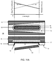
- the lower part shows a cross-section through the plate 10 while functional material is being deposited.
- the middle part shows in a view in a direction towards the surface 11 of the plate 10, a cross-section of the individual addressable resistive heating element 13.
- the upper part schematically shows the local heat flux (solid line) as a function of the position along the cavity 12 and the associated release time (dashed line).
- the cross-section of the resistive element 13 increases in a direction from left to right along the cavity 12.
- the resistive element has a resistance and therewith a heat flux that decreases in that direction, Consequently the release time for the material 50 in the cavity 12 is larger for positions more to the right end of the cavity.
- this is illustrated in that the unit of functional material is tilted with its left end towards the substrate (not shown) where it will be deposited.
- the cross-section the cross-section of the resistive element 13 is narrows at the ends of the cavity 12, and is relatively wide in a center portion.
- the resistive element has a relatively high resistance at the ends of the cavity as compared to in the center portion of the cavity.
- the resistive element provides for a relatively high heat flux at the ends of the cavity 12 as compared to the heat flux generated in between the ends, Consequently the release time for the material 50 at the ends of the cavity 12 is relatively short as compared for that of the remainder of the material 50.
- this is illustrated in that the unit of functional material 50 is curved with its ends towards the substrate (not shown) where it will be deposited.
- FIG. 11C shows a third example, wherein the cross-section of the resistive element 13 widens at the ends of the cavity 12, and has a relatively constant small width in a center portion.
- the restive element has a relatively low resistance at the ends of the cavity as compared to in the center portion of the cavity.
- the resistive element provides for a relatively low heat flux at the ends of the cavity 12 as compared to the heat flux generated in between the ends, Consequently the release time for the material 50 at the ends of the cavity 12 is relatively long as compared for that of the remainder of the material 50.
- this is illustrated in that the unit of functional material 50 is curved with its ends towards the plate 10.
- a donor area may be at level with the surrounding surface or may be formed as a cavity in the donor surface.
- a plate is provided with one or more donor areas at level with the surrounding surface and other donor areas formed as a cavity.
- a plate having a donor area formed as a cavity in the donor surface may be replaced with a plate having a donor area at level with the surrounding donor surface.
Landscapes
- Engineering & Computer Science (AREA)
- Manufacturing & Machinery (AREA)
- Microelectronics & Electronic Packaging (AREA)
- Manufacturing Of Printed Wiring (AREA)
- Control Of Resistance Heating (AREA)
- Wire Bonding (AREA)
Priority Applications (7)
| Application Number | Priority Date | Filing Date | Title |
|---|---|---|---|
| EP20174175.8A EP3911130A1 (de) | 2020-05-12 | 2020-05-12 | Transfer von viskosen materialien |
| KR1020227042790A KR20230008802A (ko) | 2020-05-12 | 2021-05-12 | 점성 물질의 전사방법 |
| CN202180041547.4A CN115700015A (zh) | 2020-05-12 | 2021-05-12 | 转移粘性材料 |
| JP2022568877A JP2023525815A (ja) | 2020-05-12 | 2021-05-12 | 粘性材料を移すこと |
| EP21727005.7A EP4151057A1 (de) | 2020-05-12 | 2021-05-12 | Übertragung von viskosen materialien |
| PCT/NL2021/050309 WO2021230746A1 (en) | 2020-05-12 | 2021-05-12 | Transferring viscous materials |
| US17/923,258 US20230240017A1 (en) | 2020-05-12 | 2021-05-12 | Transferring viscous materials |
Applications Claiming Priority (1)
| Application Number | Priority Date | Filing Date | Title |
|---|---|---|---|
| EP20174175.8A EP3911130A1 (de) | 2020-05-12 | 2020-05-12 | Transfer von viskosen materialien |
Publications (1)
| Publication Number | Publication Date |
|---|---|
| EP3911130A1 true EP3911130A1 (de) | 2021-11-17 |
Family
ID=70682635
Family Applications (2)
| Application Number | Title | Priority Date | Filing Date |
|---|---|---|---|
| EP20174175.8A Withdrawn EP3911130A1 (de) | 2020-05-12 | 2020-05-12 | Transfer von viskosen materialien |
| EP21727005.7A Pending EP4151057A1 (de) | 2020-05-12 | 2021-05-12 | Übertragung von viskosen materialien |
Family Applications After (1)
| Application Number | Title | Priority Date | Filing Date |
|---|---|---|---|
| EP21727005.7A Pending EP4151057A1 (de) | 2020-05-12 | 2021-05-12 | Übertragung von viskosen materialien |
Country Status (6)
| Country | Link |
|---|---|
| US (1) | US20230240017A1 (de) |
| EP (2) | EP3911130A1 (de) |
| JP (1) | JP2023525815A (de) |
| KR (1) | KR20230008802A (de) |
| CN (1) | CN115700015A (de) |
| WO (1) | WO2021230746A1 (de) |
Cited By (1)
| Publication number | Priority date | Publication date | Assignee | Title |
|---|---|---|---|---|
| EP4346339A1 (de) * | 2022-09-30 | 2024-04-03 | Nederlandse Organisatie voor toegepast-natuurwetenschappelijk Onderzoek TNO | Verfahren und vorrichtung zum bedrucken einer zieloberfläche eines ziels |
Families Citing this family (2)
| Publication number | Priority date | Publication date | Assignee | Title |
|---|---|---|---|---|
| EP4319486A1 (de) | 2022-08-04 | 2024-02-07 | Nederlandse Organisatie voor toegepast-natuurwetenschappelijk Onderzoek TNO | Heizplatte, heizvorrichtung mit einer heizplatte und verfahren zur herstellung einer heizplatte |
| EP4335641A1 (de) | 2022-09-08 | 2024-03-13 | Nederlandse Organisatie voor toegepast-natuurwetenschappelijk Onderzoek TNO | Verfahren und vorrichtung zum bedrucken einer zielfläche eines ziels |
Citations (5)
| Publication number | Priority date | Publication date | Assignee | Title |
|---|---|---|---|---|
| JPS61254350A (ja) * | 1985-05-08 | 1986-11-12 | Mitsubishi Electric Corp | サ−マルジエツト用記録ヘツド |
| US5760808A (en) * | 1994-04-20 | 1998-06-02 | Oce Printing Systems Gmbh | Thermoelectric printing unit for transferring an ink onto a recording medium |
| US6140009A (en) * | 1999-01-15 | 2000-10-31 | 3M Innovative Properties Company | Thermal transfer element for forming multilayer devices |
| US20120086764A1 (en) * | 2007-06-16 | 2012-04-12 | Kateeva, Inc. | Modular printhead for oled printing |
| US20170268100A1 (en) | 2016-03-16 | 2017-09-21 | Ncc Nano, Llc | Method for depositing a functional material on a substrate |
-
2020
- 2020-05-12 EP EP20174175.8A patent/EP3911130A1/de not_active Withdrawn
-
2021
- 2021-05-12 CN CN202180041547.4A patent/CN115700015A/zh active Pending
- 2021-05-12 EP EP21727005.7A patent/EP4151057A1/de active Pending
- 2021-05-12 US US17/923,258 patent/US20230240017A1/en active Pending
- 2021-05-12 WO PCT/NL2021/050309 patent/WO2021230746A1/en unknown
- 2021-05-12 KR KR1020227042790A patent/KR20230008802A/ko active Search and Examination
- 2021-05-12 JP JP2022568877A patent/JP2023525815A/ja active Pending
Patent Citations (5)
| Publication number | Priority date | Publication date | Assignee | Title |
|---|---|---|---|---|
| JPS61254350A (ja) * | 1985-05-08 | 1986-11-12 | Mitsubishi Electric Corp | サ−マルジエツト用記録ヘツド |
| US5760808A (en) * | 1994-04-20 | 1998-06-02 | Oce Printing Systems Gmbh | Thermoelectric printing unit for transferring an ink onto a recording medium |
| US6140009A (en) * | 1999-01-15 | 2000-10-31 | 3M Innovative Properties Company | Thermal transfer element for forming multilayer devices |
| US20120086764A1 (en) * | 2007-06-16 | 2012-04-12 | Kateeva, Inc. | Modular printhead for oled printing |
| US20170268100A1 (en) | 2016-03-16 | 2017-09-21 | Ncc Nano, Llc | Method for depositing a functional material on a substrate |
Cited By (2)
| Publication number | Priority date | Publication date | Assignee | Title |
|---|---|---|---|---|
| EP4346339A1 (de) * | 2022-09-30 | 2024-04-03 | Nederlandse Organisatie voor toegepast-natuurwetenschappelijk Onderzoek TNO | Verfahren und vorrichtung zum bedrucken einer zieloberfläche eines ziels |
| WO2024072220A1 (en) * | 2022-09-30 | 2024-04-04 | Nederlandse Organisatie Voor Toegepast-Natuurwetenschappelijk Onderzoek Tno | Method and device for printing a substance on a target surface of a target |
Also Published As
| Publication number | Publication date |
|---|---|
| US20230240017A1 (en) | 2023-07-27 |
| CN115700015A (zh) | 2023-02-03 |
| JP2023525815A (ja) | 2023-06-19 |
| WO2021230746A1 (en) | 2021-11-18 |
| EP4151057A1 (de) | 2023-03-22 |
| KR20230008802A (ko) | 2023-01-16 |
Similar Documents
| Publication | Publication Date | Title |
|---|---|---|
| EP3911130A1 (de) | Transfer von viskosen materialien | |
| US4769525A (en) | Circuit package attachment apparatus and method | |
| US5059756A (en) | Self regulating temperature heater with thermally conductive extensions | |
| JP3234457U (ja) | 基板上に電気的に導電性のパターンを生成するための方法および装置 | |
| US20170071062A1 (en) | Printing high aspect ratio patterns | |
| CN108831872A (zh) | 邦定结构及邦定方法 | |
| JP2013516068A (ja) | ハイパワー放熱端子を備えた表面実装抵抗器およびその製造方法 | |
| US20050266154A1 (en) | Apparatus for forming a circuit | |
| TW201811105A (zh) | 氧化鈹整體式電阻加熱器 | |
| US20230209722A1 (en) | Pattern transfer of high viscosity material | |
| US7759160B2 (en) | Method for producing conductor structures and applications thereof | |
| JP2010253503A (ja) | ヒータチップ及び接合装置 | |
| Dziedzic et al. | Fodel microresistors––processing and basic electrical properties | |
| EP1444704A1 (de) | Stromstoss chip-widerstand | |
| EP3217773B1 (de) | Verdrahtungsherstellungsverfahren und leiterplatte | |
| CN113229530A (zh) | 一种加热管和电子雾化装置及电子雾化装置的控制方法 | |
| CN111194102A (zh) | 一种发热均匀的电热板、其制备方法及厚膜加热元件 | |
| CN117855109B (zh) | 一种封装制备系统和封装制备方法 | |
| CN212010394U (zh) | 透明导电电极、调光膜、触控屏 | |
| KR20230135111A (ko) | 도너 플레이트, 증착 장치 및 증착 방법 | |
| JPH0677283A (ja) | 配線基板へのic素子の実装方法 | |
| JP3790740B2 (ja) | 定着ヒータ、定着装置および画像形成装置 | |
| JP2001113742A (ja) | 厚膜式サーマルヘッドおよびその製造方法 | |
| JP3403799B2 (ja) | 定着ヒータ、定着装置および画像形成装置 | |
| Suzuki et al. | A bonding technique for electric circuit prototyping using conductive transfer foil and soldering iron |
Legal Events
| Date | Code | Title | Description |
|---|---|---|---|
| PUAI | Public reference made under article 153(3) epc to a published international application that has entered the european phase |
Free format text: ORIGINAL CODE: 0009012 |
|
| STAA | Information on the status of an ep patent application or granted ep patent |
Free format text: STATUS: THE APPLICATION HAS BEEN PUBLISHED |
|
| AK | Designated contracting states |
Kind code of ref document: A1 Designated state(s): AL AT BE BG CH CY CZ DE DK EE ES FI FR GB GR HR HU IE IS IT LI LT LU LV MC MK MT NL NO PL PT RO RS SE SI SK SM TR |
|
| B565 | Issuance of search results under rule 164(2) epc |
Effective date: 20201028 |
|
| STAA | Information on the status of an ep patent application or granted ep patent |
Free format text: STATUS: THE APPLICATION IS DEEMED TO BE WITHDRAWN |
|
| 18D | Application deemed to be withdrawn |
Effective date: 20220518 |