EP3905347A1 - Fluorescent substrate, light-emitting substrate, and lighting device - Google Patents
Fluorescent substrate, light-emitting substrate, and lighting device Download PDFInfo
- Publication number
- EP3905347A1 EP3905347A1 EP19904987.5A EP19904987A EP3905347A1 EP 3905347 A1 EP3905347 A1 EP 3905347A1 EP 19904987 A EP19904987 A EP 19904987A EP 3905347 A1 EP3905347 A1 EP 3905347A1
- Authority
- EP
- European Patent Office
- Prior art keywords
- phosphor
- light emitting
- light
- substrate
- layer
- Prior art date
- Legal status (The legal status is an assumption and is not a legal conclusion. Google has not performed a legal analysis and makes no representation as to the accuracy of the status listed.)
- Granted
Links
Images






Classifications
-
- H—ELECTRICITY
- H10—SEMICONDUCTOR DEVICES; ELECTRIC SOLID-STATE DEVICES NOT OTHERWISE PROVIDED FOR
- H10H—INORGANIC LIGHT-EMITTING SEMICONDUCTOR DEVICES HAVING POTENTIAL BARRIERS
- H10H20/00—Individual inorganic light-emitting semiconductor devices having potential barriers, e.g. light-emitting diodes [LED]
- H10H20/80—Constructional details
- H10H20/85—Packages
- H10H20/851—Wavelength conversion means
- H10H20/8514—Wavelength conversion means characterised by their shape, e.g. plate or foil
-
- H—ELECTRICITY
- H10—SEMICONDUCTOR DEVICES; ELECTRIC SOLID-STATE DEVICES NOT OTHERWISE PROVIDED FOR
- H10H—INORGANIC LIGHT-EMITTING SEMICONDUCTOR DEVICES HAVING POTENTIAL BARRIERS
- H10H20/00—Individual inorganic light-emitting semiconductor devices having potential barriers, e.g. light-emitting diodes [LED]
- H10H20/80—Constructional details
- H10H20/85—Packages
- H10H20/851—Wavelength conversion means
- H10H20/8515—Wavelength conversion means not being in contact with the bodies
-
- H—ELECTRICITY
- H10—SEMICONDUCTOR DEVICES; ELECTRIC SOLID-STATE DEVICES NOT OTHERWISE PROVIDED FOR
- H10H—INORGANIC LIGHT-EMITTING SEMICONDUCTOR DEVICES HAVING POTENTIAL BARRIERS
- H10H20/00—Individual inorganic light-emitting semiconductor devices having potential barriers, e.g. light-emitting diodes [LED]
- H10H20/80—Constructional details
- H10H20/85—Packages
- H10H20/851—Wavelength conversion means
- H10H20/8511—Wavelength conversion means characterised by their material, e.g. binder
- H10H20/8512—Wavelength conversion materials
-
- H—ELECTRICITY
- H05—ELECTRIC TECHNIQUES NOT OTHERWISE PROVIDED FOR
- H05K—PRINTED CIRCUITS; CASINGS OR CONSTRUCTIONAL DETAILS OF ELECTRIC APPARATUS; MANUFACTURE OF ASSEMBLAGES OF ELECTRICAL COMPONENTS
- H05K1/00—Printed circuits
- H05K1/02—Details
- H05K1/0274—Optical details, e.g. printed circuits comprising integral optical means
-
- H—ELECTRICITY
- H05—ELECTRIC TECHNIQUES NOT OTHERWISE PROVIDED FOR
- H05K—PRINTED CIRCUITS; CASINGS OR CONSTRUCTIONAL DETAILS OF ELECTRIC APPARATUS; MANUFACTURE OF ASSEMBLAGES OF ELECTRICAL COMPONENTS
- H05K3/00—Apparatus or processes for manufacturing printed circuits
- H05K3/22—Secondary treatment of printed circuits
- H05K3/28—Applying non-metallic protective coatings
-
- H—ELECTRICITY
- H10—SEMICONDUCTOR DEVICES; ELECTRIC SOLID-STATE DEVICES NOT OTHERWISE PROVIDED FOR
- H10H—INORGANIC LIGHT-EMITTING SEMICONDUCTOR DEVICES HAVING POTENTIAL BARRIERS
- H10H20/00—Individual inorganic light-emitting semiconductor devices having potential barriers, e.g. light-emitting diodes [LED]
- H10H20/80—Constructional details
- H10H20/83—Electrodes
- H10H20/832—Electrodes characterised by their material
-
- H—ELECTRICITY
- H10—SEMICONDUCTOR DEVICES; ELECTRIC SOLID-STATE DEVICES NOT OTHERWISE PROVIDED FOR
- H10H—INORGANIC LIGHT-EMITTING SEMICONDUCTOR DEVICES HAVING POTENTIAL BARRIERS
- H10H20/00—Individual inorganic light-emitting semiconductor devices having potential barriers, e.g. light-emitting diodes [LED]
- H10H20/80—Constructional details
- H10H20/85—Packages
- H10H20/8506—Containers
-
- H—ELECTRICITY
- H10—SEMICONDUCTOR DEVICES; ELECTRIC SOLID-STATE DEVICES NOT OTHERWISE PROVIDED FOR
- H10H—INORGANIC LIGHT-EMITTING SEMICONDUCTOR DEVICES HAVING POTENTIAL BARRIERS
- H10H20/00—Individual inorganic light-emitting semiconductor devices having potential barriers, e.g. light-emitting diodes [LED]
- H10H20/80—Constructional details
- H10H20/85—Packages
- H10H20/857—Interconnections, e.g. lead-frames, bond wires or solder balls
-
- H—ELECTRICITY
- H10—SEMICONDUCTOR DEVICES; ELECTRIC SOLID-STATE DEVICES NOT OTHERWISE PROVIDED FOR
- H10W—GENERIC PACKAGES, INTERCONNECTIONS, CONNECTORS OR OTHER CONSTRUCTIONAL DETAILS OF DEVICES COVERED BY CLASS H10
- H10W90/00—Package configurations
-
- H—ELECTRICITY
- H05—ELECTRIC TECHNIQUES NOT OTHERWISE PROVIDED FOR
- H05K—PRINTED CIRCUITS; CASINGS OR CONSTRUCTIONAL DETAILS OF ELECTRIC APPARATUS; MANUFACTURE OF ASSEMBLAGES OF ELECTRICAL COMPONENTS
- H05K1/00—Printed circuits
- H05K1/18—Printed circuits structurally associated with non-printed electric components
- H05K1/181—Printed circuits structurally associated with non-printed electric components associated with surface mounted components
-
- H—ELECTRICITY
- H05—ELECTRIC TECHNIQUES NOT OTHERWISE PROVIDED FOR
- H05K—PRINTED CIRCUITS; CASINGS OR CONSTRUCTIONAL DETAILS OF ELECTRIC APPARATUS; MANUFACTURE OF ASSEMBLAGES OF ELECTRICAL COMPONENTS
- H05K2201/00—Indexing scheme relating to printed circuits covered by H05K1/00
- H05K2201/01—Dielectrics
- H05K2201/0104—Properties and characteristics in general
- H05K2201/0112—Absorbing light, e.g. dielectric layer with carbon filler for laser processing
-
- H—ELECTRICITY
- H05—ELECTRIC TECHNIQUES NOT OTHERWISE PROVIDED FOR
- H05K—PRINTED CIRCUITS; CASINGS OR CONSTRUCTIONAL DETAILS OF ELECTRIC APPARATUS; MANUFACTURE OF ASSEMBLAGES OF ELECTRICAL COMPONENTS
- H05K2201/00—Indexing scheme relating to printed circuits covered by H05K1/00
- H05K2201/01—Dielectrics
- H05K2201/0137—Materials
- H05K2201/0175—Inorganic, non-metallic layer, e.g. resist or dielectric for printed capacitor
-
- H—ELECTRICITY
- H05—ELECTRIC TECHNIQUES NOT OTHERWISE PROVIDED FOR
- H05K—PRINTED CIRCUITS; CASINGS OR CONSTRUCTIONAL DETAILS OF ELECTRIC APPARATUS; MANUFACTURE OF ASSEMBLAGES OF ELECTRICAL COMPONENTS
- H05K2201/00—Indexing scheme relating to printed circuits covered by H05K1/00
- H05K2201/01—Dielectrics
- H05K2201/0137—Materials
- H05K2201/0179—Thin film deposited insulating layer, e.g. inorganic layer for printed capacitor
-
- H—ELECTRICITY
- H05—ELECTRIC TECHNIQUES NOT OTHERWISE PROVIDED FOR
- H05K—PRINTED CIRCUITS; CASINGS OR CONSTRUCTIONAL DETAILS OF ELECTRIC APPARATUS; MANUFACTURE OF ASSEMBLAGES OF ELECTRICAL COMPONENTS
- H05K2201/00—Indexing scheme relating to printed circuits covered by H05K1/00
- H05K2201/09—Shape and layout
- H05K2201/09009—Substrate related
- H05K2201/09063—Holes or slots in insulating substrate not used for electrical connections
-
- H—ELECTRICITY
- H05—ELECTRIC TECHNIQUES NOT OTHERWISE PROVIDED FOR
- H05K—PRINTED CIRCUITS; CASINGS OR CONSTRUCTIONAL DETAILS OF ELECTRIC APPARATUS; MANUFACTURE OF ASSEMBLAGES OF ELECTRICAL COMPONENTS
- H05K2201/00—Indexing scheme relating to printed circuits covered by H05K1/00
- H05K2201/09—Shape and layout
- H05K2201/09209—Shape and layout details of conductors
- H05K2201/09372—Pads and lands
- H05K2201/09409—Multiple rows of pads, lands, terminals or dummy patterns; Multiple rows of mounted components
-
- H—ELECTRICITY
- H05—ELECTRIC TECHNIQUES NOT OTHERWISE PROVIDED FOR
- H05K—PRINTED CIRCUITS; CASINGS OR CONSTRUCTIONAL DETAILS OF ELECTRIC APPARATUS; MANUFACTURE OF ASSEMBLAGES OF ELECTRICAL COMPONENTS
- H05K2201/00—Indexing scheme relating to printed circuits covered by H05K1/00
- H05K2201/09—Shape and layout
- H05K2201/09209—Shape and layout details of conductors
- H05K2201/09654—Shape and layout details of conductors covering at least two types of conductors provided for in H05K2201/09218 - H05K2201/095
- H05K2201/09781—Dummy conductors, i.e. not used for normal transport of current; Dummy electrodes of components
-
- H—ELECTRICITY
- H05—ELECTRIC TECHNIQUES NOT OTHERWISE PROVIDED FOR
- H05K—PRINTED CIRCUITS; CASINGS OR CONSTRUCTIONAL DETAILS OF ELECTRIC APPARATUS; MANUFACTURE OF ASSEMBLAGES OF ELECTRICAL COMPONENTS
- H05K2201/00—Indexing scheme relating to printed circuits covered by H05K1/00
- H05K2201/10—Details of components or other objects attached to or integrated in a printed circuit board
- H05K2201/10007—Types of components
- H05K2201/10106—Light emitting diode [LED]
-
- H—ELECTRICITY
- H05—ELECTRIC TECHNIQUES NOT OTHERWISE PROVIDED FOR
- H05K—PRINTED CIRCUITS; CASINGS OR CONSTRUCTIONAL DETAILS OF ELECTRIC APPARATUS; MANUFACTURE OF ASSEMBLAGES OF ELECTRICAL COMPONENTS
- H05K2201/00—Indexing scheme relating to printed circuits covered by H05K1/00
- H05K2201/10—Details of components or other objects attached to or integrated in a printed circuit board
- H05K2201/10227—Other objects, e.g. metallic pieces
- H05K2201/10409—Screws
-
- H—ELECTRICITY
- H05—ELECTRIC TECHNIQUES NOT OTHERWISE PROVIDED FOR
- H05K—PRINTED CIRCUITS; CASINGS OR CONSTRUCTIONAL DETAILS OF ELECTRIC APPARATUS; MANUFACTURE OF ASSEMBLAGES OF ELECTRICAL COMPONENTS
- H05K2203/00—Indexing scheme relating to apparatus or processes for manufacturing printed circuits covered by H05K3/00
- H05K2203/03—Metal processing
- H05K2203/0369—Etching selective parts of a metal substrate through part of its thickness, e.g. using etch resist
-
- H—ELECTRICITY
- H05—ELECTRIC TECHNIQUES NOT OTHERWISE PROVIDED FOR
- H05K—PRINTED CIRCUITS; CASINGS OR CONSTRUCTIONAL DETAILS OF ELECTRIC APPARATUS; MANUFACTURE OF ASSEMBLAGES OF ELECTRICAL COMPONENTS
- H05K2203/00—Indexing scheme relating to apparatus or processes for manufacturing printed circuits covered by H05K3/00
- H05K2203/15—Position of the PCB during processing
- H05K2203/1572—Processing both sides of a PCB by the same process; Providing a similar arrangement of components on both sides; Making interlayer connections from two sides
-
- H—ELECTRICITY
- H10—SEMICONDUCTOR DEVICES; ELECTRIC SOLID-STATE DEVICES NOT OTHERWISE PROVIDED FOR
- H10H—INORGANIC LIGHT-EMITTING SEMICONDUCTOR DEVICES HAVING POTENTIAL BARRIERS
- H10H20/00—Individual inorganic light-emitting semiconductor devices having potential barriers, e.g. light-emitting diodes [LED]
- H10H20/01—Manufacture or treatment
- H10H20/036—Manufacture or treatment of packages
- H10H20/0361—Manufacture or treatment of packages of wavelength conversion means
Definitions
- the present invention relates to a phosphor substrate, a light emitting substrate, and a lighting device.
- Patent Document 1 discloses an LED lighting equipment including a substrate on which a light emitting element (LED element) is mounted.
- LED element light emitting element
- a reflective material is provided on a surface of the substrate to improve light emitting efficiency.
- Patent Document 1 Chinese Patent Publication No. 106163113
- An object of the present invention is to provide a phosphor substrate capable of adjusting light emitted from the phosphor substrate, in a case where a light emitting element is mounted, to light having an emission color different from light emitted by the light emitting element.
- a phosphor substrate is a phosphor substrate having at least one light emitting element mounted on one surface, and includes an insulating substrate, an electrode layer disposed on one surface of the insulating substrate and bonded to the light emitting element, and a phosphor layer which is disposed on one surface of the insulating substrate and includes a phosphor in which a light emission peak wavelength, in a case where light emitted by the light emitting element is used as excitation light, is in a visible light region, in which a surface of the electrode layer facing an outer side in a thickness direction of the insulating substrate is a flat surface, and at least a part of the phosphor layer is disposed around a bonded portion of the electrode layer with the light emitting element.
- a phosphor substrate is a phosphor substrate having a plurality of light emitting elements mounted on one surface, and includes an insulating substrate, an electrode layer disposed on one surface of the insulating substrate and bonded to each of the plurality of light emitting elements, and a phosphor layer which is provided on one surface of the insulating substrate and includes a phosphor in which a light emission peak wavelength, in a case where light emitted by the plurality of light emitting elements is used as excitation light, is in a visible light region, in which a surface of the electrode layer facing an outer side in a thickness direction of the insulating substrate is a flat surface, and at least a part of the phosphor layer is disposed around a bonded portion of the electrode layer with the light emitting element.
- the phosphor substrate according to a third aspect of the present invention according to the phosphor substrate according to the second aspect, at least a part of the phosphor layer is disposed in a region other than a region of the one surface of the insulating substrate where the electrode layer is disposed.
- the phosphor substrate according to a fourth aspect of the present invention according to the phosphor substrate according to the second or third aspect, at least a part of the phosphor layer is disposed in a portion of the electrode layer other than the bonded portion.
- a surface of the phosphor layer on the outer side in the thickness direction is positioned on the outer side in the thickness direction, compared to the flat surface.
- the light emitting element is formed as a chip sized package (CSP) in which an LED is incorporated.
- CSP chip sized package
- a correlated color temperature of the phosphor is set to a correlated color temperature which is different from a correlated color temperature of a phosphor contained in the CSP.
- the "correlated color temperature of the phosphor” means a correlated color temperature of the light emission color of the phosphor (hereinafter, the same applies).
- a correlated color temperature of the phosphor is set to a correlated color temperature which is the same as a correlated color temperature of a phosphor contained in the CSP.
- the electrode layer is formed of copper or contains copper at least on a surface, and a wavelength of light emitted by the phosphor layer is equal to or more than 600 nm.
- a light emitting substrate according to the first aspect of the present invention includes the phosphor substrate according to any one of the first to ninth aspects, and at least one light emitting element bonded to the bonded portion.
- the light emitting element is formed as a chip sized package (CSP) in which an LED is incorporated.
- CSP chip sized package
- a correlated color temperature of the phosphor is set to a correlated color temperature which is different from a correlated color temperature of a phosphor contained in the CSP.
- a correlated color temperature of the phosphor is set to a correlated color temperature which is the same as a correlated color temperature of a phosphor contained in the CSP.
- the electrode layer is formed of copper or contains copper at least on a surface, and a wavelength of light emitted by the phosphor layer is equal to or more than 600 nm.
- a lighting device of the present invention includes the light emitting substrate according to any one of the first to fourth aspects, and a power source which supplies electric power for causing the light emitting element to emit light.
- the phosphor substrate according to the first to ninth aspects of the present invention it is possible to adjust light emitted from the phosphor substrate, in a case where a light emitting element is mounted, to light having an emission color different from light emitted by the light emitting element.
- the phosphor substrate according to the second to eighth aspects of the present invention it is possible to reduce glare while adjusting light emitted from the phosphor substrate, in a case where a light emitting element is mounted, to light having an emission color different from light emitted by the light emitting element. Further, the phosphor substrate according to the eighth aspect of the present invention can also exhibit an effect of alleviating a chromaticity variation of the mounted light emitting element by the phosphor layer.
- the light emitting substrate of the present invention it is possible to adjust light emitted from the phosphor substrate to light having an emission color different from light emitted by the light emitting element.
- a configuration and function of a light emitting substrate 10 of the present embodiment will be described with reference to Figs. 1A to 1C , 2A , and 2B .
- a method for manufacturing the light emitting substrate 10 of the present embodiment will be described with reference to Figs. 3A to 3E .
- a light emitting operation of the light emitting substrate 10 of the present embodiment will be described with reference to Fig. 4 .
- effects of the present embodiment will be described with reference to Figs. 4 to 7 and the like.
- the same reference numerals are used for the same constituent elements and the description thereof will not be repeated.
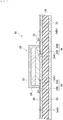
- Fig. 1A is a plan view of the light emitting substrate 10 of the present embodiment (view seen from a front surface 31), and Fig. 1B is a bottom view of the light emitting substrate 10 of the present embodiment (view seen from a rear surface 33).
- Fig. 1C is a partial cross-sectional view of the light emitting substrate 10 taken along a cutting line 1C-1C of Fig. 1A .
- the light emitting substrate 10 of the present embodiment is rectangular as an example, when seen from the front surface 31 and the rear surface 33.
- the light emitting substrate 10 of the present embodiment includes a plurality of light emitting elements 20, a phosphor substrate 30, and electronic components (not shown) such as a connector, a driver IC, and the like. That is, in the light emitting substrate 10 of the present embodiment, the plurality of light emitting elements 20 and the electronic components are mounted on the phosphor substrate 30.
- the light emitting substrate 10 of the present embodiment has a function of emitting light, in a case where power is supplied from an external power source (not shown) by directly attaching a lead wire or through a connector. Accordingly, the light emitting substrate 10 of the present embodiment is used as a main optical component in, for example, a lighting device (not shown).
- each of the plurality of light emitting elements 20 is formed as a Chip Scale Package (CSP) in which a flip chip LED 22 (hereinafter, referred to as an LED 22) is incorporated (see Fig. 1C ).
- CSP Chip Scale Package
- a flip chip LED 22 hereinafter, referred to as an LED 22
- Fig. 1C As the CSP, as shown in Fig. 1C , it is preferable that the entire circumference (five surfaces) except a bottom surface of the LED 22 is covered with a phosphor sealing layer 24.
- the phosphor sealing layer 24 contains a phosphor, and light of the LED 22 is color-converted by the phosphor of the phosphor sealing layer 24 and emitted to the outside.
- Fig. 1C Chip Scale Package
- the plurality of light emitting elements 20 are mounted on the phosphor substrate 30 in a state of being regularly arranged on the front surface 31 (an example of one surface) of the phosphor substrate 30 over the entire front surface 31.
- a correlated color temperature of the light emitted by each light emitting element 20 of the present embodiment is set to 3,018K as an example.
- the plurality of light emitting elements 20 use a heat sink (not shown) and a cooling fan (not shown) during the light emitting operation to dissipate heat (cool) the phosphor substrate 30 to be, for example, room temperature to 50°C to 100°C.
- Fig. 2A is a view of the phosphor substrate 30 of the present embodiment and is a plan view (seen from the front surface 31) in which the phosphor layer 36 omitted.
- Fig. 2B is a plan view (seen from the front surface 31) of the phosphor substrate 30 of the present embodiment.
- the bottom view of the phosphor substrate 30 of the present embodiment is the same as the view of the light emitting substrate 10 seen from the rear surface 33.
- the partial cross-sectional view of the phosphor substrate 30 of the present embodiment is the same as the view when the light emitting element 20 is removed from the partial cross-sectional view of Fig. 1C . That is, the phosphor substrate 30 of the present embodiment is rectangular as an example, when seen from the front surface 31 and the rear surface 33.
- Fig. 2A shows a range of a plurality of electrode pairs 34A which will be described later and a wiring portion 34B which is a portion other than the plurality of electrode pairs 34A, but in practice, both elements have the same flat surface, and accordingly, there is no interface between the both elements in the drawing excluding the phosphor layer 36 as Fig. 2A .
- Fig. 2A is a diagram shown with reference numerals of the plurality of electrode pairs 34A and the wiring portion 34B.
- the phosphor substrate 30 of the present embodiment includes an insulating layer 32 (an example of an insulating substrate), an electrode layer 34, a phosphor layer 36, and a rear surface pattern layer 38 (see Figs. 1B , 1C , and 2A , and 2B ).
- the phosphor layer 36 is not shown in Fig. 2A , the phosphor layer 36 is, for example, disposed on a portion of the front surface 31 of the insulating layer 32 and the electrode layer 34, other than a plurality of electrode pairs 34A which will be described later, as shown in Fig. 2B .
- the phosphor substrate 30 is formed with six through holes 39 at four portions near the four corners and two portions near the center.
- the six through holes 39 are used as positioning holes during the manufacturing of the phosphor substrate 30 and the light emitting substrate 10.
- the six through holes 39 are used as mounting screw holes for ensuring a heat-drawing effect (preventing warping and floating of the substrate) of a (light emitting) lamp housing.
- the phosphor substrate 30 of the present embodiment is manufactured by processing (etching or the like) a double-sided plate (hereinafter, referred to as a motherboard MB. see Fig. 3A ) in which copper foil layers are provided on both sides of an insulating plate, and CS-3305A manufactured by Risho Kogyo Co., Ltd. is used as an example of the motherboard MB.
- a shape thereof is, for example, rectangular when seen from the front surface 31 and the rear surface 33.
- a material thereof is, for example, an insulating material containing a bismaleimide resin and a glass cloth.
- a thickness thereof is, for example, 100 ⁇ m to 200 ⁇ m.
- Coefficients of thermal expansion (CTE) thereof in a vertical direction and a horizontal direction are, for example, equal to or less than 10 ppm/°C in a range of 50°C to 100°C, respectively. From another point of view, each of the coefficients of thermal expansion (CTE) in the vertical direction and the horizontal direction is, for example, 6 ppm/K. This value is substantially the same as that of the light emitting element 20 of the present embodiment (90% to 110%, that is, within ⁇ 10%).
- a glass transition temperature thereof is, for example, higher than 300°C.
- a storage elastic modulus is, for example, greater than 1.0 ⁇ 10 10 Pa and smaller than 1.0 ⁇ 10 11 Pa in a range of 100°C to 300°C.
- the electrode layer 34 of the present embodiment is a metal layer provided on the front surface 31 side of the insulating layer 32.
- the electrode layer 34 of this embodiment is, for example, a copper foil layer (a layer formed of Cu).
- the electrode layer 34 of the present embodiment is a flat surface formed to contain copper on at least a surface thereof (surface facing outer side in thickness direction of insulating layer 32).
- the electrode layer 34 has a pattern provided on the insulating layer 32, and is electrically connected to a terminal (not shown) to which a connector (not shown) is bonded.
- the electrode layer 34 supplies electric power supplied from an external power source (not shown) through the connector to the plurality of light emitting elements 20 at the time of configuring the light emitting substrate 10. Accordingly, a part of the electrode layer 34 is the plurality of electrode pairs 34A to which the plurality of light emitting elements 20 are bonded. That is, the electrode layer 34 of the light emitting substrate 10 of the present embodiment is disposed on the insulating layer 32 and connected to each light emitting element 20.
- the electrode layer 34 of the phosphor substrate 30 of the present embodiment is disposed on the insulating layer 32 and connected to each light emitting element 20 by each electrode pair 34A.
- the surface of each electrode pair 34A is referred to as a bonded surface 34A1 (an example of a bonded portion).
- the plurality of light emitting elements 20 of the light emitting substrate 10 of the present embodiment are regularly arranged over the entire front surface 31, the plurality of electrode pairs 34A are also arranged over the entire front surface 31 (see Fig. 2A ).
- a portion of the electrode layer 34 other than the plurality of electrode pairs 34A is referred to as a wiring portion 34B.
- the wiring portion 34B is not a portion bonded to each light emitting element 20, the surface of the wiring portion 34B is referred to as a non-bonded surface 34B1 (an example of a portion of the electrode layer 34 other than the bonded portion) in the present specification.
- a region of the front surface 31 of the insulating layer 32 where the electrode layer 34 is disposed is, for example, a region (area) that is equal to or more than 60% of the front surface 31 of the insulating layer 32 (see Fig. 2A ) .
- the phosphor layer 36 of the present embodiment is, for example, disposed on a portion of the front surface 31 of the insulating layer 32 and the electrode layer 34, other than the plurality of electrode pairs 34A. That is, the phosphor layer 36 is disposed in a region of the electrode layer 34 other than the plurality of electrode pairs 34A. In other words, at least a part of the phosphor layer 36 is disposed around each bonded surface 34A1 that is a portion of the surface 31 other than each bonded portion 34A1 (see Figs. 1C and 2B ).
- the region of the front surface 31 of the insulating layer 32 where the phosphor layer 36 is disposed is, for example, a region that is equal to or more than 80% of the front surface 31 of the insulating layer 32.
- the surface of the phosphor layer 36 on the outer side in the thickness direction of the insulating layer 32 is positioned on the outer side in the thickness direction, compared to the bonded surface 34A1 of the electrode layer 34 (see Figs. 1C and 3D ).
- the phosphor layer 36 of the present embodiment is, for example, an insulating layer containing a phosphor and a binder, which will be described later.
- the phosphor contained in the phosphor layer 36 is fine particles held in a state of being dispersed in a binder, and has a property of exciting the light emitted from the LED 22 of each light emitting element 20 as excitation light.
- the phosphor of the present embodiment has a property that the light emission peak wavelength when the light emitted by the light emitting element 20 is used as excitation light is in a visible light region.
- the binder may be, for example, an epoxy-based binder, an acrylate-based binder, or a silicone-based binder, and may have an insulating property equivalent to that of the binder contained in a solder resist.
- the phosphor contained in the phosphor layer 36 of the present embodiment is, for example, at least one or more phosphors selected from the group consisting of an ⁇ -type sialon phosphor containing Eu, a ⁇ -type sialon phosphor containing Eu, a CASN phosphor containing Eu, and a SCASN phosphor containing Eu.
- the phosphor described above is an example of the present embodiment, and may be a phosphor other than the phosphor described above, such as YAG, LuAG, BOS, and other visible light-excited phosphors.
- the ⁇ -type sialon phosphor containing Eu is represented by general formula: M x Eu y Si 12 - (m + n) Al (m + n) O n N 16-n .
- examples of a nitride phosphor include a CASN phosphor containing Eu, a SCASN phosphor containing Eu, and the like.
- the CASN phosphor containing Eu is, for example, a red phosphor which is represented by the formula CaAlSiN 3 :Eu 2+ in which Eu 2+ is used as an activator and a crystal formed of alkaline earth silicate is used as a base.
- the SCASN phosphor containing Eu is excluded.
- the SCASN phosphor containing Eu is, for example, a red phosphor which is represented by the formula (Sr,Ca)AlSiN 3 :Eu 2+ in which Eu 2+ is used as an activator and a crystal formed of alkaline earth silicate is used as a base.
- the rear surface pattern layer 38 of the present embodiment is a metal layer provided on the rear surface 33 side of the insulating layer 32.
- the rear surface pattern layer 38 of this embodiment is, for example, a copper foil layer (a layer formed of Cu).
- the rear surface pattern layer 38 is a layer in which a plurality of rectangular blocks arranged linearly along a longitudinal direction of the insulating layer 32 are arranged to be adjacent to each other by shifting phase in a short direction.
- the rear surface pattern layer 38 is, for example, an independent floating layer. In addition, the rear surface pattern layer 38 overlaps with the region that is equal to or more than 80% of the electrode layer 34 disposed on the front surface 31, for example, in a thickness direction of the insulating layer 32 (phosphor substrate 30).
- the method for manufacturing the light emitting substrate 10 of the present embodiment includes a first step, a second step, a third step, and a fourth step, and each step is performed in this order.
- Fig. 3A is a diagram showing a start time and an end time of the first step.
- the first step is a step of forming a pattern 34C that is the same as the electrode layer 34, when seen from the thickness direction, on the front surface 31 of the motherboard MB, and the rear surface pattern layer 38 on the rear surface 33. This step is performed, for example, by etching using a mask pattern (not shown).
- Fig. 3B is a diagram showing a start time and an end time of the second step.
- the second step is a step of applying a phosphor coating material 36C to the entire surface of the front surface 31 of the insulating layer 32, that is, the surface on which the electrode layer 34 is formed.
- the phosphor coating material 36C is applied by printing.
- the phosphor coating material 36C is applied thicker than the electrode layer 34.
- Fig. 3C is a diagram showing a start time and an end time of the third step.
- the third step is a step of removing a part of the phosphor layer 36 obtained by curing the phosphor coating material 36C and exposing the entire bonded surface 34A1.
- the binder of the phosphor coating material 36C is, for example, a thermosetting resin
- the phosphor coating material 36C is cured by heating and then laser light is selectively emitted to a portion of the phosphor layer 36 on each bonded surface 34A1 by using a two-dimensional laser processing device (not shown).
- a portion of the phosphor layer 36 on each bonded surface 34A1 is ablated, and each bonded surface 34A1 is exposed.
- the phosphor substrate 30 of the present embodiment is manufactured.
- this step may be performed by, for example, the following method.
- the binder of the phosphor coating material 36C is, for example, a UV curable resin (photosensitive resin)
- a mask pattern is applied to a portion (coating material opening) overlapping each bonded surface 34A1 to expose UV light, the portion other than the mask pattern is UV-cured, and a non-exposed portion (uncured portion) is removed with a resin removing liquid to expose each bonded surface 34A1.
- after-curing is performed by applying heat (photo development method).
- the phosphor layer 36 may be formed by screen printing using a screen mask (not shown) having an opening set in advance (screen printing method). In this case, a phosphor coating material opening of the screen mask at a portion overlapped with the bonded surface 34A1 may be rooted.
- Fig. 3D is a diagram showing a start time and an end time of the fourth step.
- the fourth step is a step of mounting a plurality of light emitting elements 20 on the phosphor substrate 30.
- a solder paste SP is printed on each bonded surface 34A1 of the phosphor substrate 30, and the solder paste SP is melted in a state where each electrode of the plurality of light emitting elements 20 is positioned on each bonded surface 34A1.
- each light emitting element 20 is bonded to each electrode pair 34A (each bonded surface 34A1). That is, this step is performed by, for example, a reflow step.
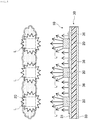
- Fig. 4 is a diagram for explaining the light emitting operation of the light emitting substrate 10 of the present embodiment.
- the power supply is started from the external power source (not shown) to the electrode layer 34 through the connector (not shown), the plurality of light emitting elements 20 emit light L radially, and some light L reaches the front surface 31 of the phosphor substrate 30.
- the behavior of the light L will be described separately according to a traveling direction of the emitted light L.
- Some light L emitted from each light emitting element 20 is emitted to the outside without being incident to the phosphor layer 36.
- a wavelength of the light L remains as the same as the wavelength of the light L, in a case of being emitted from each light emitting element 20.
- the light of the LED 22 itself in some light L emitted from each light emitting element 20 is incident to the phosphor layer 36.
- the "light of the LED 22 itself in some light L” described above is light of the emitted light L that is not color-converted by the phosphor (phosphor sealing layer 24) of each light emitting element 20 (CSP itself), that is, light of the LED 22 itself (for example, blue (wavelength is approximately 470 nm) color).
- the phosphor excites and emits excitation light.
- the reason why the phosphor is excited is that the phosphor dispersed in the phosphor layer 36 uses a phosphor (visible light excited phosphor) having an excitation peak in blue light. Along with this, a part of the energy of the light L is used for exciting the phosphor, so that the light L loses a part of the energy. As a result, the wavelength of the light L is converted (wavelength conversion is performed) . For example, depending on the type of phosphor in the phosphor layer 36 (for example, in a case where a red CASN is used as the phosphor), the wavelength of light L becomes longer (for example, 650 nm or the like).
- the excitation light in the phosphor layer 36 may be emitted from the phosphor layer 36 as it is, but some of the excitation light goes to the lower electrode layer 34. Then, some of the excitation light is emitted to the outside by reflection on the electrode layer 34.
- the wavelength of the excitation light by the phosphor of the phosphor layer 36 is equal to or more than 600 nm, the reflection effect can be expected, even if the electrode layer 34 is formed of Cu.
- the wavelength of the light L differs from the above example depending on the type of the phosphor in the phosphor layer 36, but in any case, the wavelength conversion of the light L is performed.
- a reflection effect can be expected, if the electrode layer 34 or its surface is formed of, for example, Ag (plating) .
- a white reflective layer may be provided on the lower side (insulating layer 32 side) of the phosphor layer 36.
- the reflective layer is provided with, for example, a white coating material such as a titanium oxide filler.
- the light emitting substrate 10 of the present embodiment emits a bundle of the light L, in a case of being emitted by each light emitting element 20, by setting it as a bundle of the light L containing the light L at a wavelength different from the wavelength of the light L, in a case of being emitted by each light emitting element 20, together with the excitation light.
- the light emitting substrate 10 of the present embodiment emits combined light of light (wavelength) emitted by the light emitting element 20 and light
- the light emitting substrate 10 of the present embodiment emits a bundle of the light L, in a case of being emitted by each light emitting element 20, by setting it as a bundle of the light L containing the light L at a wavelength same as the wavelength of the light L, in a case of being emitted by each light emitting element 20, together with the excitation light.
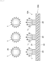
- Fig. 5 is a diagram for explaining a light emitting operation of a light emitting substrate 10A of a comparative embodiment.
- the light emitting substrate 10A of the comparative embodiment (a substrate 30A on which the plurality of light emitting elements 20 are mounted) has the same configuration as the light emitting substrate 10 (phosphor substrate 30) of the present embodiment except that the phosphor layer 36 is not provided.
- the light L emitted from each light emitting element 20 and incident to the front surface 31 of the substrate 30A is reflected or scattered without converting the wavelength. Accordingly, in the case of the substrate 30A of the comparative embodiment, it is not possible to adjust the light to light having light emission color different from the light emitted by the light emitting element 20, in a case where the light emitting element 20 is mounted. That is, in a case of the light emitting substrate 10A of the comparative embodiment, it is not possible to adjust the light to light having light emission color different from the light emitted by the light emitting element 20.
- the phosphor layer 36 when seen from the thickness direction of the insulating layer 32, the phosphor layer 36 is disposed on the surface 31 of the insulating layer 32 that is around each bonded surface 34A1 with each light emitting element 20. Accordingly, some of the light L emitted radially from each light emitting element 20 is incident to the phosphor layer 36, wavelength-converted by the phosphor layer 36, and irradiated to the outside. In this case, some of the light L radially emitted from each light emitting element 20 is incident to the phosphor layer 36 to excite the phosphor contained in the phosphor layer 36 and generate the excitation light.
- Fig. 6 is a graph showing a result of a first test of the correlated color temperature of the light emitting substrate 10 of the present embodiment.
- Fig. 7 is a graph showing a result of the second test of the correlated color temperature of the light emitting substrate 10 of the present embodiment.
- the first test is a test to obtain a result by investigating a relationship between a current (mA) and a correlated color temperature (K) of the plurality of light emitting elements 20, in a case where the power is supplied to the light emitting substrate 10 including the plurality of light emitting elements 20 having the correlated color temperature approximately at 2200 K to 2300 K to generate light.
- FLT (1) and FLT (2) indicate a case where the structure of the electrode layer 34 is the same as that of the present embodiment
- HE (1) and HE (2) show a case of an embodiment (reference example) in which, in the structure of the electrode layer 34, each bonded surface 34A1 protrudes, compared to the non-bonded surface 34B1, unlike from the present embodiment.
- the correlated color temperature of the light L emitted by the light emitting substrate 10 is lower than the correlated color temperature of the plurality of light emitting elements 20. That is, in the case of the present embodiment (including the reference example described above), the correlated color temperature could be shifted by providing the phosphor layer 36.
- the second test is a test to obtain a result by investigating a relationship between a current (mA) and a correlated color temperature (K) of the plurality of light emitting elements 20, in a case where the power is supplied to the light emitting substrate 10 including the plurality of light emitting elements 20 having the correlated color temperature approximately at 2900 K to 3000 K to generate light.
- FLT (1) and FLT (2) indicate a case where the structure of the electrode layer 34 is the same as that of the present embodiment
- HE (1) shows an embodiment (reference example) in which, in the structure of the electrode layer 34, each bonded surface 34A1 protrudes, compared to the non-bonded surface 34B1, unlike from the present embodiment.
- the correlated color temperature of the light L emitted by the light emitting substrate 10 is lower than the correlated color temperature of the plurality of light emitting elements 20. That is, in the case of the present embodiment (including the reference example described above), the correlated color temperature could be shifted by providing the phosphor layer 36.
- the phosphor substrate 30 of the present embodiment in a case where the light emitting element 20 is mounted, it is possible to adjust the light L emitted from the phosphor substrate 30 to light having a light emission color different from the light L emitted by the light emitting element 20.
- the light emitting substrate 10 of the present embodiment it is possible to adjust the light L emitted from the phosphor substrate 30 to the light L having a light emission color different from the light L emitted by the light emitting element 20.
- the light emitting substrate 10 of the present embodiment it is possible to irradiate the outside with light L having a light emission color different from the light L emitted by the light emitting element 20.
- the correlated color temperature could be shifted to the lower side, compared with the case of each reference example. That is, it can be said that, in the present embodiment, the correlated color temperature can be further decreased, compared to the reference example (embodiment in which each bonded surface 34A1 protrudes, compared to the non-bonded surface 34B1 in the structure of the electrode layer 34).
- the emission wavelength is long as in CASN
- the reflection effect of Cu in the electrode layer 34 can be obtained.
- a Cu pattern of the electrode layer 34 is used as it is as a reflective film.
- the light emitting substrate 10 of the present embodiment emits a bundle of the light L, in a case of being emitted by each light emitting element 20, by setting it as a bundle of the light L containing the light L at a wavelength same as the wavelength of the light L, in a case of being emitted by each light emitting element 20, together with the excitation light.
- spots are generated in the light L irradiated to the outside due to an arrangement interval of each light emitting element 20.
- the larger the spot of light L the larger the glare.
- each bonded surface 34A1 is surrounded (over the entire circumference) by the phosphor layer 36, and the phosphor layer 36 is also provided between the light emitting elements 20 adjacent to each other. Therefore, the excitation light is also emitted from the periphery of each bonded surface 34A1 (periphery of each light emitting element 20).
- this effect is effective, in a case where the phosphor layer 36 is provided over the entire surface of the insulating layer 32, specifically, in a case where a region of the front surface 31 of the insulating layer 32 where the phosphor layer 36 is disposed is a region that is 80% or more of the front surface 31.
- the phosphor layer 36 is provided between the adjacent light emitting elements 20 ( Fig. 2B ).
- the binder of the phosphor layer 36 has an insulating property equivalent to that of the binder contained in, for example, a solder resist. That is, in a case of the present embodiment, the phosphor layer 36 functions as a solder resist.
- the phosphor contained in the phosphor layer 36 is a CASN phosphor containing Eu, and the phosphor layer 36 is provided on the wiring portion 34B formed of Cu. Therefore, for example, in a case where each light emitting element 20 emits white light L, for example, the white light L can be adjusted to warmer light L (color having correlated color temperature shifted to the low temperature side) by the generation of the excitation light due to the CASN phosphor contained in the phosphor layer 36 and the effect of the reflection of the light L due to Cu (see Figs. 6 and 7 ).
- an example of the light emitting element 20 is a CSP.
- an example of the light emitting element 20 may be other than the CSP.
- it may simply be equipped with a flip chip.
- it can also be applied to the substrate itself of a COB device.
- the plurality of light emitting elements 20 are mounted on the phosphor substrate 30 and the light emitting substrate 10 includes the plurality of light emitting elements 20.
- the number of light emitting elements 20 mounted on the phosphor substrate 30 may be at least one or more.
- the number of light emitting elements 20 mounted on the light emitting substrate 10 may be at least one or more.
- the surface of the phosphor layer 36 on the outer side in the thickness direction of the insulating layer 32 was positioned on the outer side in the thickness direction, compared to the electrode layer 34 (see Figs. 1C and 3D ).
- the surface of the phosphor layer 36 on the outer side in the thickness direction of the insulating layer 32 is positioned at the same portion in the thickness direction as the bonded surface 34A1 of the electrode layer 34 or positioned on an inner side in the thickness direction, compared to the bonded surface 34A1, the first effect is exhibited.
- the rear surface pattern layer 38 is provided on the rear surface 33 of the phosphor substrate 30 (see Fig. 1B ).
- the first effect is exhibited even if the rear surface 33 of the phosphor substrate 30 is not provided with the rear surface pattern layer 38. Therefore, even if the embodiment is different from the phosphor substrate 30 and the light emitting substrate 10 of the present embodiment only in that the rear surface 33 is not provided with the rear surface pattern layer 38, it can be said that this embodiment belongs to the technical scope of the present invention.
- the phosphor layer 36 is, for example, disposed on a portion of the front surface 31 of the insulating layer 32 and the electrode layer 34, other than the plurality of electrode pairs 34A (see Fig. 2B ).
- the first effect is exhibited, even if the phosphor layer is not disposed over the entire region of the portion of the front surface 31 of the phosphor substrate 30 other than the plurality of electrode pair 34A.
- CS-3305A manufactured by Risho Kogyo Co., Ltd. is used as the motherboard MB in manufacturing the phosphor substrate 30 and the light emitting substrate 10.
- this is merely an example, and different motherboard MBs may be used.
- the thickness of the insulating layer, the thickness of the copper foil, and the like may not be limited to the standard specifications of those of CS-3305A manufactured by Risho Kogyo Co., Ltd., and particularly, the thickness of the copper foil may be thicker.
- the light emitting substrate 10 of the present embodiment (including the modification example thereof) can be applied to a lighting device in combination with other constituent elements.
- Other constituent elements in this case are a power source that supplies electric power for causing the light emitting element 20 of the light emitting substrate 10 to emit light, and the like.
Landscapes
- Engineering & Computer Science (AREA)
- Microelectronics & Electronic Packaging (AREA)
- Manufacturing & Machinery (AREA)
- Led Device Packages (AREA)
- Fastening Of Light Sources Or Lamp Holders (AREA)
- Non-Metallic Protective Coatings For Printed Circuits (AREA)
Abstract
Description
- The present invention relates to a phosphor substrate, a light emitting substrate, and a lighting device.
-
Patent Document 1 discloses an LED lighting equipment including a substrate on which a light emitting element (LED element) is mounted. In this LED lighting equipment, a reflective material is provided on a surface of the substrate to improve light emitting efficiency. - [Patent Document 1]
Chinese Patent Publication No. 106163113 - However, in a case of a configuration disclosed in
Patent Document 1, it is not possible to adjust light emitted by the LED lighting equipment by the reflective material to light having a light emission color different from the light emitted by the light emitting element. - An object of the present invention is to provide a phosphor substrate capable of adjusting light emitted from the phosphor substrate, in a case where a light emitting element is mounted, to light having an emission color different from light emitted by the light emitting element.
- A phosphor substrate according to a first aspect of the present invention is a phosphor substrate having at least one light emitting element mounted on one surface, and includes an insulating substrate, an electrode layer disposed on one surface of the insulating substrate and bonded to the light emitting element, and a phosphor layer which is disposed on one surface of the insulating substrate and includes a phosphor in which a light emission peak wavelength, in a case where light emitted by the light emitting element is used as excitation light, is in a visible light region, in which a surface of the electrode layer facing an outer side in a thickness direction of the insulating substrate is a flat surface, and at least a part of the phosphor layer is disposed around a bonded portion of the electrode layer with the light emitting element.
- A phosphor substrate according to a second aspect of the present invention is a phosphor substrate having a plurality of light emitting elements mounted on one surface, and includes an insulating substrate, an electrode layer disposed on one surface of the insulating substrate and bonded to each of the plurality of light emitting elements, and a phosphor layer which is provided on one surface of the insulating substrate and includes a phosphor in which a light emission peak wavelength, in a case where light emitted by the plurality of light emitting elements is used as excitation light, is in a visible light region, in which a surface of the electrode layer facing an outer side in a thickness direction of the insulating substrate is a flat surface, and at least a part of the phosphor layer is disposed around a bonded portion of the electrode layer with the light emitting element.
- In the phosphor substrate according to a third aspect of the present invention according to the phosphor substrate according to the second aspect, at least a part of the phosphor layer is disposed in a region other than a region of the one surface of the insulating substrate where the electrode layer is disposed.
- In the phosphor substrate according to a fourth aspect of the present invention according to the phosphor substrate according to the second or third aspect, at least a part of the phosphor layer is disposed in a portion of the electrode layer other than the bonded portion.
- In the phosphor substrate according to a fifth aspect of the present invention according to the phosphor substrate according to any one of the first to fourth aspects, a surface of the phosphor layer on the outer side in the thickness direction is positioned on the outer side in the thickness direction, compared to the flat surface.
- In the phosphor substrate according to a sixth aspect of the present invention according to the phosphor substrate according to any one of the first to fifth aspects, the light emitting element is formed as a chip sized package (CSP) in which an LED is incorporated.
- In the phosphor substrate according to a seventh aspect of the present invention according to the phosphor substrate according to the sixth aspect, a correlated color temperature of the phosphor is set to a correlated color temperature which is different from a correlated color temperature of a phosphor contained in the CSP.
- Here, the "correlated color temperature of the phosphor" means a correlated color temperature of the light emission color of the phosphor (hereinafter, the same applies).
- In the phosphor substrate according to an eighth aspect of the present invention according to the phosphor substrate according to the sixth aspect, a correlated color temperature of the phosphor is set to a correlated color temperature which is the same as a correlated color temperature of a phosphor contained in the CSP.
- In the phosphor substrate according to a ninth aspect of the present invention according to the phosphor substrate according to any one of the first to eighth aspects, the electrode layer is formed of copper or contains copper at least on a surface, and a wavelength of light emitted by the phosphor layer is equal to or more than 600 nm.
- A light emitting substrate according to the first aspect of the present invention includes the phosphor substrate according to any one of the first to ninth aspects, and at least one light emitting element bonded to the bonded portion.
- In the light emitting substrate according to the second aspect of the present invention according to the phosphor substrate according to the first aspect, the light emitting element is formed as a chip sized package (CSP) in which an LED is incorporated.
- In the light emitting substrate according to a third aspect of the present invention according to the phosphor substrate according to the second aspect, a correlated color temperature of the phosphor is set to a correlated color temperature which is different from a correlated color temperature of a phosphor contained in the CSP.
- In the light emitting substrate of a fourth aspect of the present invention according to the phosphor substrate of the second aspect, a correlated color temperature of the phosphor is set to a correlated color temperature which is the same as a correlated color temperature of a phosphor contained in the CSP.
- In the light emitting substrate according to a fourth aspect of the present invention according to the light emitting substrate according to any one of the first to third aspects, the electrode layer is formed of copper or contains copper at least on a surface, and a wavelength of light emitted by the phosphor layer is equal to or more than 600 nm.
- A lighting device of the present invention includes the light emitting substrate according to any one of the first to fourth aspects, and a power source which supplies electric power for causing the light emitting element to emit light.
- According to the phosphor substrate according to the first to ninth aspects of the present invention, it is possible to adjust light emitted from the phosphor substrate, in a case where a light emitting element is mounted, to light having an emission color different from light emitted by the light emitting element.
- In addition, in the phosphor substrate according to the second to eighth aspects of the present invention, it is possible to reduce glare while adjusting light emitted from the phosphor substrate, in a case where a light emitting element is mounted, to light having an emission color different from light emitted by the light emitting element. Further, the phosphor substrate according to the eighth aspect of the present invention can also exhibit an effect of alleviating a chromaticity variation of the mounted light emitting element by the phosphor layer.
- In addition, in the light emitting substrate of the present invention, it is possible to adjust light emitted from the phosphor substrate to light having an emission color different from light emitted by the light emitting element.
- The objects described above, other objects, features and advantages will be further clarified by the preferred embodiments which will be described later and the accompanying drawings below.
-
-
Fig. 1A is a plan view of a light emitting substrate of the present embodiment. -
Fig. 1B is a bottom view of the light emitting substrate of the present embodiment. -
Fig. 1C is a partial cross-sectional view of the light emitting substrate taken along a cutting line 1C-1C ofFig. 1A . -
Fig. 2A is a plan view of a phosphor substrate of the present embodiment (the phosphor layer is not shown). -
Fig. 2B is a plan view of the phosphor substrate of the present embodiment. -
Fig. 3A is an explanatory diagram of a first step in a method for manufacturing the light emitting substrate of the present embodiment. -
Fig. 3B is an explanatory diagram of a second step in the method for manufacturing the light emitting substrate of the present embodiment. -
Fig. 3C is an explanatory diagram of a third step in the method for manufacturing the light emitting substrate of the present embodiment. -
Fig. 3D is an explanatory diagram of a fourth step in the method for manufacturing the light emitting substrate according to the present embodiment. -
Fig. 4 is a diagram for explaining a light emitting operation of the light emitting substrate of the present embodiment. -
Fig. 5 is a diagram for explaining a light emitting operation of a light emitting substrate of a comparative embodiment. -
Fig. 6 is a graph showing a result of a first test of a correlated color temperature of the light emitting substrate of the present embodiment. -
Fig. 7 is a graph showing a result of a second test of the correlated color temperature of the light emitting substrate of the present embodiment. - Hereinafter, a configuration and function of a
light emitting substrate 10 of the present embodiment will be described with reference toFigs. 1A to 1C ,2A , and2B . Then, a method for manufacturing thelight emitting substrate 10 of the present embodiment will be described with reference toFigs. 3A to 3E . Next, a light emitting operation of thelight emitting substrate 10 of the present embodiment will be described with reference toFig. 4 . After that, effects of the present embodiment will be described with reference toFigs. 4 to 7 and the like. In all the drawings referred to in the following description, the same reference numerals are used for the same constituent elements and the description thereof will not be repeated. -
Fig. 1A is a plan view of thelight emitting substrate 10 of the present embodiment (view seen from a front surface 31), andFig. 1B is a bottom view of thelight emitting substrate 10 of the present embodiment (view seen from a rear surface 33).Fig. 1C is a partial cross-sectional view of thelight emitting substrate 10 taken along a cutting line 1C-1C ofFig. 1A . - The
light emitting substrate 10 of the present embodiment is rectangular as an example, when seen from thefront surface 31 and therear surface 33. In addition, thelight emitting substrate 10 of the present embodiment includes a plurality oflight emitting elements 20, aphosphor substrate 30, and electronic components (not shown) such as a connector, a driver IC, and the like. That is, in thelight emitting substrate 10 of the present embodiment, the plurality oflight emitting elements 20 and the electronic components are mounted on thephosphor substrate 30. - The
light emitting substrate 10 of the present embodiment has a function of emitting light, in a case where power is supplied from an external power source (not shown) by directly attaching a lead wire or through a connector. Accordingly, thelight emitting substrate 10 of the present embodiment is used as a main optical component in, for example, a lighting device (not shown). - As an example, each of the plurality of
light emitting elements 20 is formed as a Chip Scale Package (CSP) in which a flip chip LED 22 (hereinafter, referred to as an LED 22) is incorporated (seeFig. 1C ). As the CSP, as shown inFig. 1C , it is preferable that the entire circumference (five surfaces) except a bottom surface of theLED 22 is covered with aphosphor sealing layer 24. Thephosphor sealing layer 24 contains a phosphor, and light of theLED 22 is color-converted by the phosphor of thephosphor sealing layer 24 and emitted to the outside. As shown inFig. 1A , the plurality oflight emitting elements 20 are mounted on thephosphor substrate 30 in a state of being regularly arranged on the front surface 31 (an example of one surface) of thephosphor substrate 30 over the entirefront surface 31. A correlated color temperature of the light emitted by each light emittingelement 20 of the present embodiment is set to 3,018K as an example. In addition, the plurality oflight emitting elements 20 use a heat sink (not shown) and a cooling fan (not shown) during the light emitting operation to dissipate heat (cool) thephosphor substrate 30 to be, for example, room temperature to 50°C to 100°C. Here, to supplement the meaning of "to" used in the numerical range in the present specification, for example, "50°C to 100°C" means "equal to or higher than 50°C and equal to or lower than 100°C". In addition, "to" used in the numerical range in this specification means "equal to or more than the description part before "to" and equal to or less than the description part after "to". -
Fig. 2A is a view of thephosphor substrate 30 of the present embodiment and is a plan view (seen from the front surface 31) in which thephosphor layer 36 omitted.Fig. 2B is a plan view (seen from the front surface 31) of thephosphor substrate 30 of the present embodiment. The bottom view of thephosphor substrate 30 of the present embodiment is the same as the view of thelight emitting substrate 10 seen from therear surface 33. In addition, the partial cross-sectional view of thephosphor substrate 30 of the present embodiment is the same as the view when thelight emitting element 20 is removed from the partial cross-sectional view ofFig. 1C . That is, thephosphor substrate 30 of the present embodiment is rectangular as an example, when seen from thefront surface 31 and therear surface 33. -
Fig. 2A shows a range of a plurality ofelectrode pairs 34A which will be described later and awiring portion 34B which is a portion other than the plurality of electrode pairs 34A, but in practice, both elements have the same flat surface, and accordingly, there is no interface between the both elements in the drawing excluding thephosphor layer 36 asFig. 2A . However, in order to clarify a positional relationship between both elements,Fig. 2A is a diagram shown with reference numerals of the plurality ofelectrode pairs 34A and thewiring portion 34B. - The
phosphor substrate 30 of the present embodiment includes an insulating layer 32 (an example of an insulating substrate), anelectrode layer 34, aphosphor layer 36, and a rear surface pattern layer 38 (seeFigs. 1B ,1C , and2A , and2B ). Although thephosphor layer 36 is not shown inFig. 2A , thephosphor layer 36 is, for example, disposed on a portion of thefront surface 31 of the insulatinglayer 32 and theelectrode layer 34, other than a plurality ofelectrode pairs 34A which will be described later, as shown inFig. 2B . - In addition, as shown in
Figs. 1B and2A , thephosphor substrate 30 is formed with six throughholes 39 at four portions near the four corners and two portions near the center. The six throughholes 39 are used as positioning holes during the manufacturing of thephosphor substrate 30 and thelight emitting substrate 10. In addition, the six throughholes 39 are used as mounting screw holes for ensuring a heat-drawing effect (preventing warping and floating of the substrate) of a (light emitting) lamp housing. As will be described later, thephosphor substrate 30 of the present embodiment is manufactured by processing (etching or the like) a double-sided plate (hereinafter, referred to as a motherboard MB. seeFig. 3A ) in which copper foil layers are provided on both sides of an insulating plate, and CS-3305A manufactured by Risho Kogyo Co., Ltd. is used as an example of the motherboard MB. - Hereinafter, main features of the insulating
layer 32 of the present embodiment will be described. - As described above, a shape thereof is, for example, rectangular when seen from the
front surface 31 and therear surface 33. - A material thereof is, for example, an insulating material containing a bismaleimide resin and a glass cloth.
- A thickness thereof is, for example, 100 µm to 200 µm.
- Coefficients of thermal expansion (CTE) thereof in a vertical direction and a horizontal direction are, for example, equal to or less than 10 ppm/°C in a range of 50°C to 100°C, respectively. From another point of view, each of the coefficients of thermal expansion (CTE) in the vertical direction and the horizontal direction is, for example, 6 ppm/K. This value is substantially the same as that of the
light emitting element 20 of the present embodiment (90% to 110%, that is, within ± 10%). - A glass transition temperature thereof is, for example, higher than 300°C.
- A storage elastic modulus is, for example, greater than 1.0 × 10¹⁰ Pa and smaller than 1.0 × 10¹¹ Pa in a range of 100°C to 300°C.
- The
electrode layer 34 of the present embodiment is a metal layer provided on thefront surface 31 side of the insulatinglayer 32. Theelectrode layer 34 of this embodiment is, for example, a copper foil layer (a layer formed of Cu). In other words, theelectrode layer 34 of the present embodiment is a flat surface formed to contain copper on at least a surface thereof (surface facing outer side in thickness direction of insulating layer 32). - The
electrode layer 34 has a pattern provided on the insulatinglayer 32, and is electrically connected to a terminal (not shown) to which a connector (not shown) is bonded. Theelectrode layer 34 supplies electric power supplied from an external power source (not shown) through the connector to the plurality oflight emitting elements 20 at the time of configuring thelight emitting substrate 10. Accordingly, a part of theelectrode layer 34 is the plurality of electrode pairs 34A to which the plurality oflight emitting elements 20 are bonded. That is, theelectrode layer 34 of thelight emitting substrate 10 of the present embodiment is disposed on the insulatinglayer 32 and connected to each light emittingelement 20. From another point of view, theelectrode layer 34 of thephosphor substrate 30 of the present embodiment is disposed on the insulatinglayer 32 and connected to each light emittingelement 20 by eachelectrode pair 34A. Here, in the present specification, the surface of eachelectrode pair 34A is referred to as a bonded surface 34A1 (an example of a bonded portion). - In addition, as described above, since the plurality of
light emitting elements 20 of thelight emitting substrate 10 of the present embodiment are regularly arranged over the entirefront surface 31, the plurality of electrode pairs 34A are also arranged over the entire front surface 31 (seeFig. 2A ). A portion of theelectrode layer 34 other than the plurality ofelectrode pairs 34A is referred to as awiring portion 34B. Here, since thewiring portion 34B is not a portion bonded to each light emittingelement 20, the surface of thewiring portion 34B is referred to as a non-bonded surface 34B1 (an example of a portion of theelectrode layer 34 other than the bonded portion) in the present specification. - A region of the
front surface 31 of the insulatinglayer 32 where theelectrode layer 34 is disposed (occupied area of the electrode layer 34) is, for example, a region (area) that is equal to or more than 60% of thefront surface 31 of the insulating layer 32 (seeFig. 2A ) . - As shown in
Fig. 2B , thephosphor layer 36 of the present embodiment is, for example, disposed on a portion of thefront surface 31 of the insulatinglayer 32 and theelectrode layer 34, other than the plurality of electrode pairs 34A. That is, thephosphor layer 36 is disposed in a region of theelectrode layer 34 other than the plurality of electrode pairs 34A. In other words, at least a part of thephosphor layer 36 is disposed around each bonded surface 34A1 that is a portion of thesurface 31 other than each bonded portion 34A1 (seeFigs. 1C and2B ). In addition, from another point of view, at least a part of thephosphor layer 36 is disposed so as to surround each bonded surface 34A1 over the entire circumference, when seen from thesurface 31 side. As a result, the plurality of bonded portions 34A1 are set by each opening of thephosphor layer 36. In the present embodiment, the region of thefront surface 31 of the insulatinglayer 32 where thephosphor layer 36 is disposed is, for example, a region that is equal to or more than 80% of thefront surface 31 of the insulatinglayer 32. - The surface of the
phosphor layer 36 on the outer side in the thickness direction of the insulatinglayer 32 is positioned on the outer side in the thickness direction, compared to the bonded surface 34A1 of the electrode layer 34 (seeFigs. 1C and3D ). - The
phosphor layer 36 of the present embodiment is, for example, an insulating layer containing a phosphor and a binder, which will be described later. The phosphor contained in thephosphor layer 36 is fine particles held in a state of being dispersed in a binder, and has a property of exciting the light emitted from theLED 22 of each light emittingelement 20 as excitation light. Specifically, the phosphor of the present embodiment has a property that the light emission peak wavelength when the light emitted by thelight emitting element 20 is used as excitation light is in a visible light region. The binder may be, for example, an epoxy-based binder, an acrylate-based binder, or a silicone-based binder, and may have an insulating property equivalent to that of the binder contained in a solder resist. - Here, the phosphor contained in the
phosphor layer 36 of the present embodiment is, for example, at least one or more phosphors selected from the group consisting of an α-type sialon phosphor containing Eu, a β-type sialon phosphor containing Eu, a CASN phosphor containing Eu, and a SCASN phosphor containing Eu. The phosphor described above is an example of the present embodiment, and may be a phosphor other than the phosphor described above, such as YAG, LuAG, BOS, and other visible light-excited phosphors. - The α-type sialon phosphor containing Eu is represented by general formula: MxEuySi12 - (m + n)Al(m + n)OnN16-n. In the above general formula, M is at least one or more elements containing at least Ca selected from the group consisting of Li, Mg, Ca, Y, and lanthanide elements (here, excluding La and Ce), and in a case where a valence of M is a, ax + 2y = m, x satisfies 0 < x ≦ 1.5, 0.3 ≦ m < 4.5, and 0 < n < 2.25.
- The β-type sialon phosphor containing Eu is a phosphor in which divalent europium (Eu2+) is dissolved as a light emitting center in β-type sialon represented by general formula: Si6-zAlzOzN8-z (z = 0.005 to 1) .
- In addition, examples of a nitride phosphor include a CASN phosphor containing Eu, a SCASN phosphor containing Eu, and the like.
- The CASN phosphor containing Eu (an example of a nitride phosphor) is, for example, a red phosphor which is represented by the formula CaAlSiN3:Eu2+ in which Eu2+ is used as an activator and a crystal formed of alkaline earth silicate is used as a base. In the definition of the CASN phosphor containing Eu in the present specification, the SCASN phosphor containing Eu is excluded.
- The SCASN phosphor containing Eu (an example of a nitride phosphor) is, for example, a red phosphor which is represented by the formula (Sr,Ca)AlSiN3:Eu2+ in which Eu2+ is used as an activator and a crystal formed of alkaline earth silicate is used as a base.
- The rear
surface pattern layer 38 of the present embodiment is a metal layer provided on therear surface 33 side of the insulatinglayer 32. The rearsurface pattern layer 38 of this embodiment is, for example, a copper foil layer (a layer formed of Cu). - As shown in
Fig. 1B , the rearsurface pattern layer 38 is a layer in which a plurality of rectangular blocks arranged linearly along a longitudinal direction of the insulatinglayer 32 are arranged to be adjacent to each other by shifting phase in a short direction. - The rear
surface pattern layer 38 is, for example, an independent floating layer. In addition, the rearsurface pattern layer 38 overlaps with the region that is equal to or more than 80% of theelectrode layer 34 disposed on thefront surface 31, for example, in a thickness direction of the insulating layer 32 (phosphor substrate 30). - The above is the description of the configuration of the
light emitting substrate 10 and thephosphor substrate 30 of the present embodiment. - Next, a method for manufacturing the
light emitting substrate 10 of the present embodiment will be described with reference toFigs. 3A to 3D . The method for manufacturing thelight emitting substrate 10 of the present embodiment includes a first step, a second step, a third step, and a fourth step, and each step is performed in this order. -
Fig. 3A is a diagram showing a start time and an end time of the first step. The first step is a step of forming a pattern 34C that is the same as theelectrode layer 34, when seen from the thickness direction, on thefront surface 31 of the motherboard MB, and the rearsurface pattern layer 38 on therear surface 33. This step is performed, for example, by etching using a mask pattern (not shown). -
Fig. 3B is a diagram showing a start time and an end time of the second step. The second step is a step of applying aphosphor coating material 36C to the entire surface of thefront surface 31 of the insulatinglayer 32, that is, the surface on which theelectrode layer 34 is formed. In this step, for example, thephosphor coating material 36C is applied by printing. In this case, thephosphor coating material 36C is applied thicker than theelectrode layer 34. -
Fig. 3C is a diagram showing a start time and an end time of the third step. The third step is a step of removing a part of thephosphor layer 36 obtained by curing thephosphor coating material 36C and exposing the entire bonded surface 34A1. Here, in a case where the binder of thephosphor coating material 36C is, for example, a thermosetting resin, thephosphor coating material 36C is cured by heating and then laser light is selectively emitted to a portion of thephosphor layer 36 on each bonded surface 34A1 by using a two-dimensional laser processing device (not shown). As a result, a portion of thephosphor layer 36 on each bonded surface 34A1 is ablated, and each bonded surface 34A1 is exposed. As a result of the above, thephosphor substrate 30 of the present embodiment is manufactured. - In addition to the above method, this step may be performed by, for example, the following method. In a case where the binder of the
phosphor coating material 36C is, for example, a UV curable resin (photosensitive resin), a mask pattern is applied to a portion (coating material opening) overlapping each bonded surface 34A1 to expose UV light, the portion other than the mask pattern is UV-cured, and a non-exposed portion (uncured portion) is removed with a resin removing liquid to expose each bonded surface 34A1. After that, in general, after-curing is performed by applying heat (photo development method). - In addition, instead of the second step and the third step, the
phosphor layer 36 may be formed by screen printing using a screen mask (not shown) having an opening set in advance (screen printing method). In this case, a phosphor coating material opening of the screen mask at a portion overlapped with the bonded surface 34A1 may be rooted. -
Fig. 3D is a diagram showing a start time and an end time of the fourth step. The fourth step is a step of mounting a plurality oflight emitting elements 20 on thephosphor substrate 30. In this step, a solder paste SP is printed on each bonded surface 34A1 of thephosphor substrate 30, and the solder paste SP is melted in a state where each electrode of the plurality oflight emitting elements 20 is positioned on each bonded surface 34A1. After that, in a case where the solder paste SP is cooled and solidified, eachlight emitting element 20 is bonded to eachelectrode pair 34A (each bonded surface 34A1). That is, this step is performed by, for example, a reflow step. - The above is the description of the method for manufacturing the
light emitting substrate 10 of the present embodiment. - Next, the light emitting operation of the
light emitting substrate 10 of the present embodiment will be described with reference toFig. 4. Fig. 4 is a diagram for explaining the light emitting operation of thelight emitting substrate 10 of the present embodiment. - First, in a case where an operation switch (not shown) for operating the plurality of
light emitting elements 20 is turned on, the power supply is started from the external power source (not shown) to theelectrode layer 34 through the connector (not shown), the plurality oflight emitting elements 20 emit light L radially, and some light L reaches thefront surface 31 of thephosphor substrate 30. Hereinafter, the behavior of the light L will be described separately according to a traveling direction of the emitted light L. - Some light L emitted from each light emitting
element 20 is emitted to the outside without being incident to thephosphor layer 36. In this case, a wavelength of the light L remains as the same as the wavelength of the light L, in a case of being emitted from each light emittingelement 20. - In addition, the light of the
LED 22 itself in some light L emitted from each light emittingelement 20 is incident to thephosphor layer 36. Here, the "light of theLED 22 itself in some light L" described above is light of the emitted light L that is not color-converted by the phosphor (phosphor sealing layer 24) of each light emitting element 20 (CSP itself), that is, light of theLED 22 itself (for example, blue (wavelength is approximately 470 nm) color). Then, in a case where the light L of theLED 22 itself collides with the phosphor dispersed in thephosphor layer 36, the phosphor excites and emits excitation light. Here, the reason why the phosphor is excited is that the phosphor dispersed in thephosphor layer 36 uses a phosphor (visible light excited phosphor) having an excitation peak in blue light. Along with this, a part of the energy of the light L is used for exciting the phosphor, so that the light L loses a part of the energy. As a result, the wavelength of the light L is converted (wavelength conversion is performed) . For example, depending on the type of phosphor in the phosphor layer 36 (for example, in a case where a red CASN is used as the phosphor), the wavelength of light L becomes longer (for example, 650 nm or the like). In addition, the excitation light in thephosphor layer 36 may be emitted from thephosphor layer 36 as it is, but some of the excitation light goes to thelower electrode layer 34. Then, some of the excitation light is emitted to the outside by reflection on theelectrode layer 34. As described above, in a case where the wavelength of the excitation light by the phosphor of thephosphor layer 36 is equal to or more than 600 nm, the reflection effect can be expected, even if theelectrode layer 34 is formed of Cu. The wavelength of the light L differs from the above example depending on the type of the phosphor in thephosphor layer 36, but in any case, the wavelength conversion of the light L is performed. For example, in a case where the wavelength of the excitation light is less than 600 nm, a reflection effect can be expected, if theelectrode layer 34 or its surface is formed of, for example, Ag (plating) . In addition, a white reflective layer may be provided on the lower side (insulatinglayer 32 side) of thephosphor layer 36. The reflective layer is provided with, for example, a white coating material such as a titanium oxide filler. - As described above, the light L emitted by each light emitting element 20 (the light L emitted radially by each light emitting element 20) is irradiated to the outside together with the excitation light through a plurality of optical paths as described above. Therefore, in a case where a light emission wavelength of the phosphor contained in the
phosphor layer 36 and a light emission wavelength of the phosphor (phosphor sealing layer 24) that seals (or covers) theLED 22 of the light emitting element 20 (CSP) are different from each other, thelight emitting substrate 10 of the present embodiment emits a bundle of the light L, in a case of being emitted by each light emittingelement 20, by setting it as a bundle of the light L containing the light L at a wavelength different from the wavelength of the light L, in a case of being emitted by each light emittingelement 20, together with the excitation light. For example, thelight emitting substrate 10 of the present embodiment emits combined light of light (wavelength) emitted by thelight emitting element 20 and light (wavelength) emitted from thephosphor layer 36. - Meanwhile, in a case where a light emission wavelength of the phosphor contained in the
phosphor layer 36 and a light emission wavelength of the phosphor (phosphor sealing layer 24) that seals (or covers) theLED 22 of the light emitting element 20 (CSP) are the same as each other (in a case of the same correlated color temperature), thelight emitting substrate 10 of the present embodiment emits a bundle of the light L, in a case of being emitted by each light emittingelement 20, by setting it as a bundle of the light L containing the light L at a wavelength same as the wavelength of the light L, in a case of being emitted by each light emittingelement 20, together with the excitation light. - The above is the description of the light emitting operation of the
light emitting substrate 10 of the present embodiment. - Next, the effect of the present embodiment will be described with reference to the drawings.
- The first effect will be described by comparing the present embodiment with a comparative embodiment (see
Fig. 5 ) described below. Here, in the description of the comparative embodiment, in a case of using the same constituent elements and the like as in the present embodiment, the same names, symbols, and the like as in the case of the present embodiment are used for the constituent elements and the like.Fig. 5 is a diagram for explaining a light emitting operation of alight emitting substrate 10A of a comparative embodiment. Thelight emitting substrate 10A of the comparative embodiment (asubstrate 30A on which the plurality oflight emitting elements 20 are mounted) has the same configuration as the light emitting substrate 10 (phosphor substrate 30) of the present embodiment except that thephosphor layer 36 is not provided. - In the case of the
light emitting substrate 10A of the comparative embodiment, the light L emitted from each light emittingelement 20 and incident to thefront surface 31 of thesubstrate 30A is reflected or scattered without converting the wavelength. Accordingly, in the case of thesubstrate 30A of the comparative embodiment, it is not possible to adjust the light to light having light emission color different from the light emitted by thelight emitting element 20, in a case where thelight emitting element 20 is mounted. That is, in a case of thelight emitting substrate 10A of the comparative embodiment, it is not possible to adjust the light to light having light emission color different from the light emitted by thelight emitting element 20. - On the other hand, in the case of the present embodiment, when seen from the thickness direction of the insulating
layer 32, thephosphor layer 36 is disposed on thesurface 31 of the insulatinglayer 32 that is around each bonded surface 34A1 with each light emittingelement 20. Accordingly, some of the light L emitted radially from each light emittingelement 20 is incident to thephosphor layer 36, wavelength-converted by thephosphor layer 36, and irradiated to the outside. In this case, some of the light L radially emitted from each light emittingelement 20 is incident to thephosphor layer 36 to excite the phosphor contained in thephosphor layer 36 and generate the excitation light. - Here,
Fig. 6 is a graph showing a result of a first test of the correlated color temperature of thelight emitting substrate 10 of the present embodiment. In addition,Fig. 7 is a graph showing a result of the second test of the correlated color temperature of thelight emitting substrate 10 of the present embodiment. - The first test is a test to obtain a result by investigating a relationship between a current (mA) and a correlated color temperature (K) of the plurality of
light emitting elements 20, in a case where the power is supplied to thelight emitting substrate 10 including the plurality oflight emitting elements 20 having the correlated color temperature approximately at 2200 K to 2300 K to generate light. Here, FLT (1) and FLT (2) indicate a case where the structure of theelectrode layer 34 is the same as that of the present embodiment, and HE (1) and HE (2) show a case of an embodiment (reference example) in which, in the structure of theelectrode layer 34, each bonded surface 34A1 protrudes, compared to the non-bonded surface 34B1, unlike from the present embodiment. As the result ofFig. 6 , in any case, the correlated color temperature of the light L emitted by thelight emitting substrate 10 is lower than the correlated color temperature of the plurality oflight emitting elements 20. That is, in the case of the present embodiment (including the reference example described above), the correlated color temperature could be shifted by providing thephosphor layer 36. - In addition, the second test is a test to obtain a result by investigating a relationship between a current (mA) and a correlated color temperature (K) of the plurality of
light emitting elements 20, in a case where the power is supplied to thelight emitting substrate 10 including the plurality oflight emitting elements 20 having the correlated color temperature approximately at 2900 K to 3000 K to generate light. Here, FLT (1) and FLT (2) indicate a case where the structure of theelectrode layer 34 is the same as that of the present embodiment, and HE (1) shows an embodiment (reference example) in which, in the structure of theelectrode layer 34, each bonded surface 34A1 protrudes, compared to the non-bonded surface 34B1, unlike from the present embodiment. As the result ofFig. 7 , in any case, the correlated color temperature of the light L emitted by thelight emitting substrate 10 is lower than the correlated color temperature of the plurality oflight emitting elements 20. That is, in the case of the present embodiment (including the reference example described above), the correlated color temperature could be shifted by providing thephosphor layer 36. - Therefore, according to the
phosphor substrate 30 of the present embodiment, in a case where thelight emitting element 20 is mounted, it is possible to adjust the light L emitted from thephosphor substrate 30 to light having a light emission color different from the light L emitted by thelight emitting element 20. Along with this, according to thelight emitting substrate 10 of the present embodiment, it is possible to adjust the light L emitted from thephosphor substrate 30 to the light L having a light emission color different from the light L emitted by thelight emitting element 20. From another point of view, according to thelight emitting substrate 10 of the present embodiment, it is possible to irradiate the outside with light L having a light emission color different from the light L emitted by thelight emitting element 20. - As shown in the results of the first test and the second test, in the case of the present embodiment, the correlated color temperature could be shifted to the lower side, compared with the case of each reference example. That is, it can be said that, in the present embodiment, the correlated color temperature can be further decreased, compared to the reference example (embodiment in which each bonded surface 34A1 protrudes, compared to the non-bonded surface 34B1 in the structure of the electrode layer 34). This indicates that, in a case where the emission wavelength is long as in CASN, the reflection effect of Cu in the
electrode layer 34 can be obtained. Then, in a case where the emission wavelength of the phosphor contained in thephosphor layer 36 is equal to or more than 600 nm, it can be proposed that a Cu pattern of theelectrode layer 34 is used as it is as a reflective film. - Meanwhile, in a case where a light emission wavelength of the phosphor contained in the
phosphor layer 36 and a light emission wavelength of the phosphor (phosphor sealing layer 24) that seals (or covers) theLED 22 of the light emitting element 20 (CSP) are the same as each other (in a case of the same correlated color temperature), thelight emitting substrate 10 of the present embodiment emits a bundle of the light L, in a case of being emitted by each light emittingelement 20, by setting it as a bundle of the light L containing the light L at a wavelength same as the wavelength of the light L, in a case of being emitted by each light emittingelement 20, together with the excitation light. In this case, it is possible to exhibit the effect of alleviating a chromaticity variation of the mountedlight emitting element 20 by thephosphor layer 36. - In the case of the comparative embodiment, as shown in
Fig. 5 , spots are generated in the light L irradiated to the outside due to an arrangement interval of each light emittingelement 20. Here, the larger the spot of light L, the larger the glare. - On the other hand, in a case of the present embodiment, as shown in
Fig. 2B , the periphery of each bonded surface 34A1 is surrounded (over the entire circumference) by thephosphor layer 36, and thephosphor layer 36 is also provided between thelight emitting elements 20 adjacent to each other. Therefore, the excitation light is also emitted from the periphery of each bonded surface 34A1 (periphery of each light emitting element 20). - Therefore, according to the present embodiment, it is possible to reduce the glare, compared to the comparative embodiment.
- In particular, this effect is effective, in a case where the
phosphor layer 36 is provided over the entire surface of the insulatinglayer 32, specifically, in a case where a region of thefront surface 31 of the insulatinglayer 32 where thephosphor layer 36 is disposed is a region that is 80% or more of thefront surface 31. - In addition, in the present embodiment, as described above, the
phosphor layer 36 is provided between the adjacent light emitting elements 20 (Fig. 2B ). In addition, the binder of thephosphor layer 36 has an insulating property equivalent to that of the binder contained in, for example, a solder resist. That is, in a case of the present embodiment, thephosphor layer 36 functions as a solder resist. - In addition, in a case of the present embodiment, for example, the phosphor contained in the
phosphor layer 36 is a CASN phosphor containing Eu, and thephosphor layer 36 is provided on thewiring portion 34B formed of Cu. Therefore, for example, in a case where each light emittingelement 20 emits white light L, for example, the white light L can be adjusted to warmer light L (color having correlated color temperature shifted to the low temperature side) by the generation of the excitation light due to the CASN phosphor contained in thephosphor layer 36 and the effect of the reflection of the light L due to Cu (seeFigs. 6 and7 ). - The above is the description of the effect of the present embodiment.
- As described above, the present invention has been described with reference to the embodiments and examples described above, but the present invention is not limited to the embodiments and examples described above. The technical scope of the present invention also includes, for example, the following embodiments (modification example).
- For example, in the description of the present embodiment, an example of the
light emitting element 20 is a CSP. However, an example of thelight emitting element 20 may be other than the CSP. For example, it may simply be equipped with a flip chip. In addition, it can also be applied to the substrate itself of a COB device. - In addition, in the description of the present embodiment, the plurality of
light emitting elements 20 are mounted on thephosphor substrate 30 and thelight emitting substrate 10 includes the plurality oflight emitting elements 20. However, considering a mechanism for explaining a first effect described above, it is clear that the first effect is exhibited even with onelight emitting element 20. Therefore, the number oflight emitting elements 20 mounted on thephosphor substrate 30 may be at least one or more. In addition, the number oflight emitting elements 20 mounted on thelight emitting substrate 10 may be at least one or more. - In addition, in the description of the present embodiment, the surface of the
phosphor layer 36 on the outer side in the thickness direction of the insulatinglayer 32 was positioned on the outer side in the thickness direction, compared to the electrode layer 34 (seeFigs. 1C and3D ). However, considering a mechanism for describing the first effect described above, it is clear that, although the surface of thephosphor layer 36 on the outer side in the thickness direction of the insulatinglayer 32 is positioned at the same portion in the thickness direction as the bonded surface 34A1 of theelectrode layer 34 or positioned on an inner side in the thickness direction, compared to the bonded surface 34A1, the first effect is exhibited. - In addition, in the description of the present embodiment, the rear
surface pattern layer 38 is provided on therear surface 33 of the phosphor substrate 30 (seeFig. 1B ). However, considering a mechanism for explaining the first effect described above, it is clear that the first effect is exhibited even if therear surface 33 of thephosphor substrate 30 is not provided with the rearsurface pattern layer 38. Therefore, even if the embodiment is different from thephosphor substrate 30 and thelight emitting substrate 10 of the present embodiment only in that therear surface 33 is not provided with the rearsurface pattern layer 38, it can be said that this embodiment belongs to the technical scope of the present invention. - In addition, in the description of the present embodiment, the
phosphor layer 36 is, for example, disposed on a portion of thefront surface 31 of the insulatinglayer 32 and theelectrode layer 34, other than the plurality ofelectrode pairs 34A (seeFig. 2B ). However, considering a mechanism for explaining the first effect described above, it is clear that the first effect is exhibited, even if the phosphor layer is not disposed over the entire region of the portion of thefront surface 31 of thephosphor substrate 30 other than the plurality ofelectrode pair 34A. Therefore, even if the embodiment is different from thephosphor substrate 30 and thelight emitting substrate 10 of the present embodiment only in that thephosphor layer 36 is disposed in a range of thefront surface 31 different from that of the present embodiment, it can be said that this embodiment belongs to the technical scope of the present invention. - In addition, in the description of the present embodiment, it has been described that CS-3305A manufactured by Risho Kogyo Co., Ltd. is used as the motherboard MB in manufacturing the
phosphor substrate 30 and thelight emitting substrate 10. However, this is merely an example, and different motherboard MBs may be used. For example, the thickness of the insulating layer, the thickness of the copper foil, and the like may not be limited to the standard specifications of those of CS-3305A manufactured by Risho Kogyo Co., Ltd., and particularly, the thickness of the copper foil may be thicker. - The
light emitting substrate 10 of the present embodiment (including the modification example thereof) can be applied to a lighting device in combination with other constituent elements. Other constituent elements in this case are a power source that supplies electric power for causing thelight emitting element 20 of thelight emitting substrate 10 to emit light, and the like. - This application claims priority based on
Japanese Patent Application No. 2018-244544
Claims (15)
- A phosphor substrate having at least one light emitting element mounted on one surface, the phosphor substrate comprising:an insulating substrate;an electrode layer disposed on one surface of the insulating substrate and bonded to the light emitting element; anda phosphor layer which is disposed on one surface of the insulating substrate and includes a phosphor in which a light emission peak wavelength, in a case where light emitted by the light emitting element is used as excitation light, is in a visible light region,wherein a surface of the electrode layer facing an outer side in a thickness direction of the insulating substrate is a flat surface, andat least a part of the phosphor layer is disposed around a bonded portion of the electrode layer with the light emitting element.
- A phosphor substrate having a plurality of light emitting elements mounted on one surface, the phosphor substrate comprising:an insulating substrate;an electrode layer which is disposed on one surface of the insulating substrate and bonded to the plurality of light emitting elements; anda phosphor layer which is provided on one surface of the insulating substrate and includes a phosphor in which a light emission peak wavelength, in a case where light emitted by the plurality of light emitting elements is used as excitation light, is in a visible light region,wherein a surface of the electrode layer facing an outer side in a thickness direction of the insulating substrate is a flat surface, andat least a part of the phosphor layer is disposed around a bonded portion of the electrode layer with the light emitting element.
- The phosphor substrate according to claim 2,
wherein at least a part of the phosphor layer is disposed in a region other than a region of the one surface of the insulating substrate where the electrode layer is disposed. - The phosphor substrate according to claim 2 or 3,
wherein at least a part of the phosphor layer is disposed in a portion of the electrode layer other than the bonded portion. - The phosphor substrate according to any one of claims 1 to 4,
wherein a surface of the phosphor layer on the outer side in the thickness direction is positioned on the outer side in the thickness direction, compared to the flat surface. - The phosphor substrate according to any one of claims 1 to 5,
wherein the light emitting element is formed as a chip sized package (CSP) in which an LED is incorporated. - The phosphor substrate according to claim 6,
wherein a correlated color temperature of the phosphor is set to a correlated color temperature which is different from a correlated color temperature of a phosphor contained in the CSP. - The phosphor substrate according to claim 6,
wherein a correlated color temperature of the phosphor is set to a correlated color temperature which is the same as a correlated color temperature of a phosphor contained in the CSP. - The phosphor substrate according to any one of claims 1 to 8,wherein the electrode layer is formed of copper or contains copper at least on a surface, anda wavelength of light emitted by the phosphor layer is equal to or more than 600 nm.
- A light emitting substrate comprising:the phosphor substrate according to any one of claims 1 to 9; andat least one light emitting element bonded to the bonded portion.
- The light emitting substrate according to claim 10,
wherein the light emitting element is formed as a chip sized package (CSP) in which an LED is incorporated. - The light emitting substrate according to claim 11,
wherein a correlated color temperature of the phosphor is set to a correlated color temperature which is different from a correlated color temperature of a phosphor contained in the CSP. - The light emitting substrate according to claim 11,
wherein a correlated color temperature of the phosphor is set to a correlated color temperature which is the same as a correlated color temperature of a phosphor contained in the CSP. - The light emitting substrate according to any one of claims 10 to 13,wherein the electrode layer is formed of copper or contains copper at least on a surface, anda wavelength of the light emitted by the phosphor layer is equal to or more than 600 nm.
- A lighting device comprising:the light emitting substrate according to any one of claims 10 to 14; anda power source which supplies electric power for causing the light emitting element to emit light.
Applications Claiming Priority (2)
| Application Number | Priority Date | Filing Date | Title |
|---|---|---|---|
| JP2018244544 | 2018-12-27 | ||
| PCT/JP2019/049689 WO2020137762A1 (en) | 2018-12-27 | 2019-12-18 | Fluorescent substrate, light-emitting substrate, and lighting device |
Publications (3)
| Publication Number | Publication Date |
|---|---|
| EP3905347A1 true EP3905347A1 (en) | 2021-11-03 |
| EP3905347A4 EP3905347A4 (en) | 2022-02-16 |
| EP3905347B1 EP3905347B1 (en) | 2024-02-21 |
Family
ID=71129752
Family Applications (1)
| Application Number | Title | Priority Date | Filing Date |
|---|---|---|---|
| EP19904987.5A Active EP3905347B1 (en) | 2018-12-27 | 2019-12-18 | Light-emitting substrate, and lighting device |
Country Status (7)
| Country | Link |
|---|---|
| US (1) | US12068438B2 (en) |
| EP (1) | EP3905347B1 (en) |
| JP (1) | JP7410881B2 (en) |
| KR (1) | KR102872843B1 (en) |
| CN (1) | CN113228315B (en) |
| TW (1) | TWI842799B (en) |
| WO (1) | WO2020137762A1 (en) |
Families Citing this family (3)
| Publication number | Priority date | Publication date | Assignee | Title |
|---|---|---|---|---|
| CN113228313B (en) * | 2018-12-27 | 2025-01-07 | 电化株式会社 | Phosphor substrate, light-emitting substrate, and lighting device |
| WO2022045013A1 (en) * | 2020-08-28 | 2022-03-03 | デンカ株式会社 | Phosphor substrate, light-emitting substrate, and lighting device |
| US12338974B2 (en) * | 2021-03-22 | 2025-06-24 | Denka Company Limited | Light source unit and road illumination device equipped with light source unit |
Family Cites Families (87)
| Publication number | Priority date | Publication date | Assignee | Title |
|---|---|---|---|---|
| JP3992770B2 (en) | 1996-11-22 | 2007-10-17 | 日亜化学工業株式会社 | Light emitting device and method for forming the same |
| JP2000011953A (en) * | 1998-06-25 | 2000-01-14 | Nec Corp | Fluorescent lamp formed from multi-tube |
| JP3640153B2 (en) | 1999-11-18 | 2005-04-20 | 松下電工株式会社 | Illumination light source |
| JP2001148509A (en) | 1999-11-18 | 2001-05-29 | Matsushita Electric Works Ltd | Illumination light source |
| JP3970056B2 (en) | 2002-03-01 | 2007-09-05 | シチズン電子株式会社 | Light emitting device and manufacturing method thereof |
| JP2005191420A (en) * | 2003-12-26 | 2005-07-14 | Stanley Electric Co Ltd | Semiconductor light emitting device having wavelength conversion layer and manufacturing method thereof |
| JP4128564B2 (en) | 2004-04-27 | 2008-07-30 | 松下電器産業株式会社 | Light emitting device |
| KR100887489B1 (en) | 2004-04-27 | 2009-03-10 | 파나소닉 주식회사 | Phosphor composition and method for producing the same, and light-emitting device using the same |
| JP5219331B2 (en) * | 2005-09-13 | 2013-06-26 | 株式会社住田光学ガラス | Method for manufacturing solid element device |
| KR20070047676A (en) | 2005-11-02 | 2007-05-07 | 가부시끼가이샤 도리온 | LED Mounting Board |
| JP2008066691A (en) * | 2006-03-10 | 2008-03-21 | Toshiba Lighting & Technology Corp | Lighting device |
| JP3863174B2 (en) | 2006-05-08 | 2006-12-27 | 東芝電子エンジニアリング株式会社 | Light emitting device |
| US7808013B2 (en) | 2006-10-31 | 2010-10-05 | Cree, Inc. | Integrated heat spreaders for light emitting devices (LEDs) and related assemblies |
| TWI343664B (en) | 2007-07-06 | 2011-06-11 | Formosa Epitaxy Inc | Light-blending light-emitting diode |
| TWI361497B (en) | 2007-08-20 | 2012-04-01 | Delta Electronics Inc | Light-emitting diode apparatus and manufacturing method thereof |
| KR101361575B1 (en) | 2007-09-17 | 2014-02-13 | 삼성전자주식회사 | Light Emitting Diode package and method of manufacturing the same |
| JP5211667B2 (en) | 2007-12-07 | 2013-06-12 | ソニー株式会社 | Lighting device and display device |
| US8558438B2 (en) | 2008-03-01 | 2013-10-15 | Goldeneye, Inc. | Fixtures for large area directional and isotropic solid state lighting panels |
| JP2009267289A (en) * | 2008-04-30 | 2009-11-12 | Citizen Electronics Co Ltd | Light-emitting device |
| JP5345363B2 (en) | 2008-06-24 | 2013-11-20 | シャープ株式会社 | Light emitting device |
| EP2448026A4 (en) | 2009-06-26 | 2013-08-14 | Asahi Rubber Inc | REFLECTIVE MATERIAL OF WHITE COLOR AND PRODUCTION PROCESS |
| KR101601622B1 (en) * | 2009-10-13 | 2016-03-09 | 삼성전자주식회사 | Light emitting diode device, light emitting device and method of manufacturing light emitting diode device |
| EP2315284A3 (en) | 2009-10-21 | 2013-03-27 | Toshiba Lighting & Technology Corporation | Light-Emitting apparatus and luminaire |
| CN102074558B (en) | 2009-10-21 | 2013-06-19 | 东芝照明技术株式会社 | Lighting device and lighting fixture |
| US20110215348A1 (en) | 2010-02-03 | 2011-09-08 | Soraa, Inc. | Reflection Mode Package for Optical Devices Using Gallium and Nitrogen Containing Materials |
| KR20130038847A (en) | 2010-03-23 | 2013-04-18 | 가부시키가이샤 아사히 러버 | Silicone resin reflective substrate, manufacturing method for same, and base material composition used in reflective substrate |
| TWI446590B (en) | 2010-09-30 | 2014-07-21 | 億光電子工業股份有限公司 | Light-emitting diode package structure and manufacturing method thereof |
| JP2012094578A (en) | 2010-10-25 | 2012-05-17 | Citizen Holdings Co Ltd | Manufacturing method of semiconductor light emitting device |
| JP5661552B2 (en) * | 2010-12-24 | 2015-01-28 | シチズンホールディングス株式会社 | Semiconductor light emitting device and manufacturing method thereof |
| JP2012186274A (en) | 2011-03-04 | 2012-09-27 | Sharp Corp | Light-emitting device, led chip, led wafer and package substrate |
| JP5703997B2 (en) | 2011-06-29 | 2015-04-22 | 豊田合成株式会社 | Light emitting device |
| EP2787543B1 (en) | 2011-11-29 | 2017-03-22 | Sharp Kabushiki Kaisha | Manufacturing method for light-emitting device |
| JP2013115368A (en) | 2011-11-30 | 2013-06-10 | Rohm Co Ltd | Led module |
| JP5984199B2 (en) | 2011-12-26 | 2016-09-06 | シチズン電子株式会社 | Light emitting device |
| KR20130104975A (en) * | 2012-03-16 | 2013-09-25 | 삼성전자주식회사 | Light emitting device |
| WO2013153739A1 (en) | 2012-04-11 | 2013-10-17 | パナソニック株式会社 | Light-emitting device, and lamp |
| US20150155441A1 (en) | 2012-06-15 | 2015-06-04 | Andrei Alexeev | LED package and method for producing the same |
| JP5910340B2 (en) | 2012-06-15 | 2016-04-27 | コニカミノルタ株式会社 | LED device and manufacturing method thereof |
| TW201405894A (en) | 2012-07-27 | 2014-02-01 | 華夏光股份有限公司 | Thermoelectrically separated semiconductor device and its manufacturing method |
| JP2014220431A (en) | 2013-05-09 | 2014-11-20 | 日東電工株式会社 | Circuit board, optical semiconductor device and method of manufacturing the same |
| US9287472B2 (en) | 2013-06-27 | 2016-03-15 | Nichia Corporation | Light emitting device and method of manufacturing the same |
| CN103346241B (en) | 2013-07-03 | 2015-09-30 | 梁栌伊 | The encapsulating structure of white led lamps |
| CN104282819B (en) | 2013-07-08 | 2018-08-28 | 光宝电子(广州)有限公司 | Flip-chip light-emitting diode packaging module and manufacturing method thereof |
| KR20160030225A (en) | 2013-07-10 | 2016-03-16 | 골든아이 인코퍼레이티드 | Self cooling light source |
| US9673364B2 (en) | 2013-07-19 | 2017-06-06 | Nichia Corporation | Light emitting device and method of manufacturing the same |
| KR102123039B1 (en) | 2013-07-19 | 2020-06-15 | 니치아 카가쿠 고교 가부시키가이샤 | Light emitting device and method of manufacturing the same |
| JP6277860B2 (en) | 2013-07-19 | 2018-02-14 | 日亜化学工業株式会社 | Light emitting device and manufacturing method thereof |
| WO2015011925A1 (en) * | 2013-07-24 | 2015-01-29 | コニカミノルタ株式会社 | Led device production method |
| ES2629079T3 (en) | 2013-08-01 | 2017-08-07 | Philips Lighting Holding B.V. | Light emission arrangement with adapted output spectrum |
| JP6195760B2 (en) * | 2013-08-16 | 2017-09-13 | シチズン電子株式会社 | LED light emitting device |
| US20150060911A1 (en) | 2013-09-05 | 2015-03-05 | Unistars Corporation | Optoelectronic semiconductor device and fabricating method thereof |
| JP6955704B2 (en) | 2013-10-23 | 2021-10-27 | 株式会社光波 | Light emitting device |
| JP6299176B2 (en) | 2013-11-22 | 2018-03-28 | 日亜化学工業株式会社 | LIGHT EMITTING DEVICE, ITS MANUFACTURING METHOD, AND LIGHTING DEVICE EQUIPPED WITH THE LIGHT EMITTING DEVICE |
| JP6435705B2 (en) | 2013-12-27 | 2018-12-12 | 日亜化学工業株式会社 | Collective substrate, light-emitting device, and light-emitting element inspection method |
| KR102098245B1 (en) * | 2014-02-11 | 2020-04-07 | 삼성전자 주식회사 | Light source package and a display device including the same |
| CN103904072A (en) | 2014-03-28 | 2014-07-02 | 中山市鸿宝电业有限公司 | High-power LED chip integrated packaging structure |
| CN203839375U (en) | 2014-03-28 | 2014-09-17 | 中山市鸿宝电业有限公司 | Large-power LED chip integrated packaging structure |
| TWI613391B (en) | 2014-04-01 | 2018-02-01 | 晶元光電股份有限公司 | Light-emitting diode assembly and light-emitting diode bulb using the same |
| JP2015216139A (en) | 2014-05-07 | 2015-12-03 | 株式会社小糸製作所 | Light emitting module |
| US10741735B2 (en) | 2014-06-02 | 2020-08-11 | 3M Innovative Properties Company | LED with remote phosphor and shell reflector |
| US9660161B2 (en) * | 2014-07-07 | 2017-05-23 | Cree, Inc. | Light emitting diode (LED) components including contact expansion frame |
| JP2016069401A (en) | 2014-09-26 | 2016-05-09 | 住友ベークライト株式会社 | Prepreg, resin substrate, metal-clad laminate, printed wiring board, and semiconductor device |
| TWM496850U (en) | 2014-10-23 | 2015-03-01 | Genesis Photonics Inc | LED package structure |
| CN107148685B (en) | 2014-10-28 | 2019-12-06 | 夏普株式会社 | Substrate, light-emitting device, and lighting device |
| JP6681139B2 (en) | 2014-12-24 | 2020-04-15 | 日亜化学工業株式会社 | Light emitting device |
| JP2016139632A (en) | 2015-01-26 | 2016-08-04 | 京セラ株式会社 | Wiring board |
| CN106163113A (en) | 2015-03-23 | 2016-11-23 | 李玉俊 | LED installs lamp bead circuit board light-reflection layer processing technology |
| US10347798B2 (en) | 2015-06-01 | 2019-07-09 | Intematix Corporation | Photoluminescence material coating of LED chips |
| TWI644454B (en) | 2015-08-19 | 2018-12-11 | 佰鴻工業股份有限公司 | Light-emitting diode structure |
| JP2017041621A (en) | 2015-08-23 | 2017-02-23 | 久豊技研株式会社 | LED light emitting device |
| JP6582794B2 (en) | 2015-09-18 | 2019-10-02 | 大日本印刷株式会社 | LED information display panel with snow melting function and LED information display device |
| US9985182B2 (en) | 2015-12-25 | 2018-05-29 | Citizen Electronics Co., Ltd. | Light-emitting apparatus and color-matching apparatus |
| US10797209B2 (en) | 2016-02-05 | 2020-10-06 | Maven Optronics Co., Ltd. | Light emitting device with beam shaping structure and manufacturing method of the same |
| TWI583028B (en) | 2016-02-05 | 2017-05-11 | 行家光電股份有限公司 | Light-emitting device with light-shaped adjustment structure and method of manufacturing same |
| JP6669248B2 (en) | 2016-03-31 | 2020-03-18 | 株式会社村田製作所 | Circuit module |
| JP6724634B2 (en) | 2016-07-28 | 2020-07-15 | 日亜化学工業株式会社 | Method for manufacturing light emitting device |
| CN107093658A (en) * | 2016-09-30 | 2017-08-25 | 深圳市玲涛光电科技有限公司 | Light-emitting component, backlight source module and electronic equipment |
| JP6751910B2 (en) | 2016-10-05 | 2020-09-09 | パナソニックIpマネジメント株式会社 | Manufacturing method of multi-layer printed wiring board and multi-layer printed wiring board |
| JP2018082027A (en) | 2016-11-16 | 2018-05-24 | 豊田合成株式会社 | Light emitting device and manufacturing method thereof |
| CN106356439A (en) | 2016-11-21 | 2017-01-25 | 中山市立体光电科技有限公司 | An LED packaging structure with adjustable color temperature |
| JP6472467B2 (en) | 2017-01-23 | 2019-02-20 | Nissha株式会社 | Capacitive touch panel |
| JP6797314B2 (en) * | 2017-11-13 | 2020-12-09 | デンカ株式会社 | Lighting device with mounting board for LED lighting |
| JP2019093339A (en) | 2017-11-22 | 2019-06-20 | 帝人フロンティア株式会社 | Moisture permeable filter medium |
| EP3546895B1 (en) | 2018-03-28 | 2020-05-27 | E+E Elektronik Ges.M.B.H. | Device and method for operating a heatable sensor, in particular in an explosive atmosphere |
| KR102653215B1 (en) | 2018-10-10 | 2024-04-01 | 삼성전기주식회사 | Multilayer ceramic electronic component |
| CN113228313B (en) | 2018-12-27 | 2025-01-07 | 电化株式会社 | Phosphor substrate, light-emitting substrate, and lighting device |
| KR102872847B1 (en) | 2018-12-27 | 2025-10-20 | 덴카 주식회사 | Phosphor substrate, light-emitting substrate and lighting device |
-
2019
- 2019-12-18 JP JP2020563143A patent/JP7410881B2/en active Active
- 2019-12-18 WO PCT/JP2019/049689 patent/WO2020137762A1/en not_active Ceased
- 2019-12-18 US US17/415,448 patent/US12068438B2/en active Active
- 2019-12-18 CN CN201980085492.XA patent/CN113228315B/en active Active
- 2019-12-18 EP EP19904987.5A patent/EP3905347B1/en active Active
- 2019-12-18 KR KR1020217018338A patent/KR102872843B1/en active Active
- 2019-12-23 TW TW108147175A patent/TWI842799B/en active
Also Published As
| Publication number | Publication date |
|---|---|
| KR102872843B1 (en) | 2025-10-21 |
| CN113228315A (en) | 2021-08-06 |
| TW202031871A (en) | 2020-09-01 |
| JPWO2020137762A1 (en) | 2021-11-11 |
| US12068438B2 (en) | 2024-08-20 |
| US20220278257A1 (en) | 2022-09-01 |
| EP3905347B1 (en) | 2024-02-21 |
| CN113228315B (en) | 2024-11-05 |
| JP7410881B2 (en) | 2024-01-10 |
| TWI842799B (en) | 2024-05-21 |
| WO2020137762A1 (en) | 2020-07-02 |
| KR20210106433A (en) | 2021-08-30 |
| EP3905347A4 (en) | 2022-02-16 |
Similar Documents
| Publication | Publication Date | Title |
|---|---|---|
| US12100788B2 (en) | Phosphor substrate, light emitting substrate, and lighting device | |
| EP3905345B1 (en) | Light-emitting substrate, and lighting device | |
| US12068438B2 (en) | Phosphor substrate, light emitting substrate, and lighting device | |
| US20230361254A1 (en) | Phosphor board manufacturing method and light-emitting substrate manufacturing method | |
| US12107196B2 (en) | Phosphor substrate, light emitting substrate, and lighting device | |
| US12027652B2 (en) | Phosphor substrate, light emitting substrate, and lighting device | |
| JP7523550B2 (en) | Phosphor substrate, light-emitting substrate, and lighting device |
Legal Events
| Date | Code | Title | Description |
|---|---|---|---|
| STAA | Information on the status of an ep patent application or granted ep patent |
Free format text: STATUS: THE INTERNATIONAL PUBLICATION HAS BEEN MADE |
|
| PUAI | Public reference made under article 153(3) epc to a published international application that has entered the european phase |
Free format text: ORIGINAL CODE: 0009012 |
|
| STAA | Information on the status of an ep patent application or granted ep patent |
Free format text: STATUS: REQUEST FOR EXAMINATION WAS MADE |
|
| 17P | Request for examination filed |
Effective date: 20210701 |
|
| AK | Designated contracting states |
Kind code of ref document: A1 Designated state(s): AL AT BE BG CH CY CZ DE DK EE ES FI FR GB GR HR HU IE IS IT LI LT LU LV MC MK MT NL NO PL PT RO RS SE SI SK SM TR |
|
| A4 | Supplementary search report drawn up and despatched |
Effective date: 20220118 |
|
| RIC1 | Information provided on ipc code assigned before grant |
Ipc: H05K 3/28 20060101ALI20220112BHEP Ipc: H01L 33/62 20100101ALI20220112BHEP Ipc: H01L 25/075 20060101ALI20220112BHEP Ipc: H01L 33/50 20100101AFI20220112BHEP |
|
| DAV | Request for validation of the european patent (deleted) | ||
| DAX | Request for extension of the european patent (deleted) | ||
| STAA | Information on the status of an ep patent application or granted ep patent |
Free format text: STATUS: EXAMINATION IS IN PROGRESS |
|
| 17Q | First examination report despatched |
Effective date: 20221018 |
|
| GRAP | Despatch of communication of intention to grant a patent |
Free format text: ORIGINAL CODE: EPIDOSNIGR1 |
|
| STAA | Information on the status of an ep patent application or granted ep patent |
Free format text: STATUS: GRANT OF PATENT IS INTENDED |
|
| INTG | Intention to grant announced |
Effective date: 20231011 |
|
| GRAS | Grant fee paid |
Free format text: ORIGINAL CODE: EPIDOSNIGR3 |
|
| GRAA | (expected) grant |
Free format text: ORIGINAL CODE: 0009210 |
|
| STAA | Information on the status of an ep patent application or granted ep patent |
Free format text: STATUS: THE PATENT HAS BEEN GRANTED |
|
| AK | Designated contracting states |
Kind code of ref document: B1 Designated state(s): AL AT BE BG CH CY CZ DE DK EE ES FI FR GB GR HR HU IE IS IT LI LT LU LV MC MK MT NL NO PL PT RO RS SE SI SK SM TR |
|
| REG | Reference to a national code |
Ref country code: GB Ref legal event code: FG4D |
|
| REG | Reference to a national code |
Ref country code: CH Ref legal event code: EP |
|
| REG | Reference to a national code |
Ref country code: DE Ref legal event code: R096 Ref document number: 602019047121 Country of ref document: DE |
|
| REG | Reference to a national code |
Ref country code: IE Ref legal event code: FG4D |
|
| P01 | Opt-out of the competence of the unified patent court (upc) registered |
Effective date: 20240208 |
|
| REG | Reference to a national code |
Ref country code: NL Ref legal event code: FP |
|
| REG | Reference to a national code |
Ref country code: LT Ref legal event code: MG9D |
|
| PG25 | Lapsed in a contracting state [announced via postgrant information from national office to epo] |
Ref country code: IS Free format text: LAPSE BECAUSE OF FAILURE TO SUBMIT A TRANSLATION OF THE DESCRIPTION OR TO PAY THE FEE WITHIN THE PRESCRIBED TIME-LIMIT Effective date: 20240621 |
|
| PG25 | Lapsed in a contracting state [announced via postgrant information from national office to epo] |
Ref country code: LT Free format text: LAPSE BECAUSE OF FAILURE TO SUBMIT A TRANSLATION OF THE DESCRIPTION OR TO PAY THE FEE WITHIN THE PRESCRIBED TIME-LIMIT Effective date: 20240221 |
|
| PG25 | Lapsed in a contracting state [announced via postgrant information from national office to epo] |
Ref country code: GR Free format text: LAPSE BECAUSE OF FAILURE TO SUBMIT A TRANSLATION OF THE DESCRIPTION OR TO PAY THE FEE WITHIN THE PRESCRIBED TIME-LIMIT Effective date: 20240522 |
|
| REG | Reference to a national code |
Ref country code: AT Ref legal event code: MK05 Ref document number: 1659882 Country of ref document: AT Kind code of ref document: T Effective date: 20240221 |
|
| PG25 | Lapsed in a contracting state [announced via postgrant information from national office to epo] |
Ref country code: RS Free format text: LAPSE BECAUSE OF FAILURE TO SUBMIT A TRANSLATION OF THE DESCRIPTION OR TO PAY THE FEE WITHIN THE PRESCRIBED TIME-LIMIT Effective date: 20240521 Ref country code: HR Free format text: LAPSE BECAUSE OF FAILURE TO SUBMIT A TRANSLATION OF THE DESCRIPTION OR TO PAY THE FEE WITHIN THE PRESCRIBED TIME-LIMIT Effective date: 20240221 |
|
| PG25 | Lapsed in a contracting state [announced via postgrant information from national office to epo] |
Ref country code: ES Free format text: LAPSE BECAUSE OF FAILURE TO SUBMIT A TRANSLATION OF THE DESCRIPTION OR TO PAY THE FEE WITHIN THE PRESCRIBED TIME-LIMIT Effective date: 20240221 |
|
| PG25 | Lapsed in a contracting state [announced via postgrant information from national office to epo] |
Ref country code: AT Free format text: LAPSE BECAUSE OF FAILURE TO SUBMIT A TRANSLATION OF THE DESCRIPTION OR TO PAY THE FEE WITHIN THE PRESCRIBED TIME-LIMIT Effective date: 20240221 |
|
| PG25 | Lapsed in a contracting state [announced via postgrant information from national office to epo] |
Ref country code: RS Free format text: LAPSE BECAUSE OF FAILURE TO SUBMIT A TRANSLATION OF THE DESCRIPTION OR TO PAY THE FEE WITHIN THE PRESCRIBED TIME-LIMIT Effective date: 20240521 Ref country code: NO Free format text: LAPSE BECAUSE OF FAILURE TO SUBMIT A TRANSLATION OF THE DESCRIPTION OR TO PAY THE FEE WITHIN THE PRESCRIBED TIME-LIMIT Effective date: 20240521 Ref country code: LT Free format text: LAPSE BECAUSE OF FAILURE TO SUBMIT A TRANSLATION OF THE DESCRIPTION OR TO PAY THE FEE WITHIN THE PRESCRIBED TIME-LIMIT Effective date: 20240221 Ref country code: IS Free format text: LAPSE BECAUSE OF FAILURE TO SUBMIT A TRANSLATION OF THE DESCRIPTION OR TO PAY THE FEE WITHIN THE PRESCRIBED TIME-LIMIT Effective date: 20240621 Ref country code: HR Free format text: LAPSE BECAUSE OF FAILURE TO SUBMIT A TRANSLATION OF THE DESCRIPTION OR TO PAY THE FEE WITHIN THE PRESCRIBED TIME-LIMIT Effective date: 20240221 Ref country code: GR Free format text: LAPSE BECAUSE OF FAILURE TO SUBMIT A TRANSLATION OF THE DESCRIPTION OR TO PAY THE FEE WITHIN THE PRESCRIBED TIME-LIMIT Effective date: 20240522 Ref country code: FI Free format text: LAPSE BECAUSE OF FAILURE TO SUBMIT A TRANSLATION OF THE DESCRIPTION OR TO PAY THE FEE WITHIN THE PRESCRIBED TIME-LIMIT Effective date: 20240221 Ref country code: ES Free format text: LAPSE BECAUSE OF FAILURE TO SUBMIT A TRANSLATION OF THE DESCRIPTION OR TO PAY THE FEE WITHIN THE PRESCRIBED TIME-LIMIT Effective date: 20240221 Ref country code: BG Free format text: LAPSE BECAUSE OF FAILURE TO SUBMIT A TRANSLATION OF THE DESCRIPTION OR TO PAY THE FEE WITHIN THE PRESCRIBED TIME-LIMIT Effective date: 20240221 Ref country code: AT Free format text: LAPSE BECAUSE OF FAILURE TO SUBMIT A TRANSLATION OF THE DESCRIPTION OR TO PAY THE FEE WITHIN THE PRESCRIBED TIME-LIMIT Effective date: 20240221 |
|
| PG25 | Lapsed in a contracting state [announced via postgrant information from national office to epo] |
Ref country code: PT Free format text: LAPSE BECAUSE OF FAILURE TO SUBMIT A TRANSLATION OF THE DESCRIPTION OR TO PAY THE FEE WITHIN THE PRESCRIBED TIME-LIMIT Effective date: 20240621 Ref country code: PL Free format text: LAPSE BECAUSE OF FAILURE TO SUBMIT A TRANSLATION OF THE DESCRIPTION OR TO PAY THE FEE WITHIN THE PRESCRIBED TIME-LIMIT Effective date: 20240221 |
|
| PG25 | Lapsed in a contracting state [announced via postgrant information from national office to epo] |
Ref country code: SE Free format text: LAPSE BECAUSE OF FAILURE TO SUBMIT A TRANSLATION OF THE DESCRIPTION OR TO PAY THE FEE WITHIN THE PRESCRIBED TIME-LIMIT Effective date: 20240221 Ref country code: PT Free format text: LAPSE BECAUSE OF FAILURE TO SUBMIT A TRANSLATION OF THE DESCRIPTION OR TO PAY THE FEE WITHIN THE PRESCRIBED TIME-LIMIT Effective date: 20240621 Ref country code: PL Free format text: LAPSE BECAUSE OF FAILURE TO SUBMIT A TRANSLATION OF THE DESCRIPTION OR TO PAY THE FEE WITHIN THE PRESCRIBED TIME-LIMIT Effective date: 20240221 Ref country code: LV Free format text: LAPSE BECAUSE OF FAILURE TO SUBMIT A TRANSLATION OF THE DESCRIPTION OR TO PAY THE FEE WITHIN THE PRESCRIBED TIME-LIMIT Effective date: 20240221 |
|
| PG25 | Lapsed in a contracting state [announced via postgrant information from national office to epo] |
Ref country code: DK Free format text: LAPSE BECAUSE OF FAILURE TO SUBMIT A TRANSLATION OF THE DESCRIPTION OR TO PAY THE FEE WITHIN THE PRESCRIBED TIME-LIMIT Effective date: 20240221 |
|
| PG25 | Lapsed in a contracting state [announced via postgrant information from national office to epo] |
Ref country code: SM Free format text: LAPSE BECAUSE OF FAILURE TO SUBMIT A TRANSLATION OF THE DESCRIPTION OR TO PAY THE FEE WITHIN THE PRESCRIBED TIME-LIMIT Effective date: 20240221 |
|
| PG25 | Lapsed in a contracting state [announced via postgrant information from national office to epo] |
Ref country code: EE Free format text: LAPSE BECAUSE OF FAILURE TO SUBMIT A TRANSLATION OF THE DESCRIPTION OR TO PAY THE FEE WITHIN THE PRESCRIBED TIME-LIMIT Effective date: 20240221 Ref country code: CZ Free format text: LAPSE BECAUSE OF FAILURE TO SUBMIT A TRANSLATION OF THE DESCRIPTION OR TO PAY THE FEE WITHIN THE PRESCRIBED TIME-LIMIT Effective date: 20240221 |
|
| PG25 | Lapsed in a contracting state [announced via postgrant information from national office to epo] |
Ref country code: SK Free format text: LAPSE BECAUSE OF FAILURE TO SUBMIT A TRANSLATION OF THE DESCRIPTION OR TO PAY THE FEE WITHIN THE PRESCRIBED TIME-LIMIT Effective date: 20240221 |
|
| PG25 | Lapsed in a contracting state [announced via postgrant information from national office to epo] |
Ref country code: SM Free format text: LAPSE BECAUSE OF FAILURE TO SUBMIT A TRANSLATION OF THE DESCRIPTION OR TO PAY THE FEE WITHIN THE PRESCRIBED TIME-LIMIT Effective date: 20240221 Ref country code: SK Free format text: LAPSE BECAUSE OF FAILURE TO SUBMIT A TRANSLATION OF THE DESCRIPTION OR TO PAY THE FEE WITHIN THE PRESCRIBED TIME-LIMIT Effective date: 20240221 Ref country code: RO Free format text: LAPSE BECAUSE OF FAILURE TO SUBMIT A TRANSLATION OF THE DESCRIPTION OR TO PAY THE FEE WITHIN THE PRESCRIBED TIME-LIMIT Effective date: 20240221 Ref country code: EE Free format text: LAPSE BECAUSE OF FAILURE TO SUBMIT A TRANSLATION OF THE DESCRIPTION OR TO PAY THE FEE WITHIN THE PRESCRIBED TIME-LIMIT Effective date: 20240221 Ref country code: DK Free format text: LAPSE BECAUSE OF FAILURE TO SUBMIT A TRANSLATION OF THE DESCRIPTION OR TO PAY THE FEE WITHIN THE PRESCRIBED TIME-LIMIT Effective date: 20240221 Ref country code: CZ Free format text: LAPSE BECAUSE OF FAILURE TO SUBMIT A TRANSLATION OF THE DESCRIPTION OR TO PAY THE FEE WITHIN THE PRESCRIBED TIME-LIMIT Effective date: 20240221 |
|
| REG | Reference to a national code |
Ref country code: DE Ref legal event code: R097 Ref document number: 602019047121 Country of ref document: DE Ref country code: DE Ref legal event code: R079 Ref document number: 602019047121 Country of ref document: DE Free format text: PREVIOUS MAIN CLASS: H01L0033500000 Ipc: H10H0020851000 |
|
| PLBE | No opposition filed within time limit |
Free format text: ORIGINAL CODE: 0009261 |
|
| STAA | Information on the status of an ep patent application or granted ep patent |
Free format text: STATUS: NO OPPOSITION FILED WITHIN TIME LIMIT |
|
| PGFP | Annual fee paid to national office [announced via postgrant information from national office to epo] |
Ref country code: DE Payment date: 20241029 Year of fee payment: 6 |
|
| PGFP | Annual fee paid to national office [announced via postgrant information from national office to epo] |
Ref country code: GB Payment date: 20241104 Year of fee payment: 6 |
|
| PGFP | Annual fee paid to national office [announced via postgrant information from national office to epo] |
Ref country code: FR Payment date: 20241111 Year of fee payment: 6 |
|
| PGFP | Annual fee paid to national office [announced via postgrant information from national office to epo] |
Ref country code: IT Payment date: 20241112 Year of fee payment: 6 |
|
| 26N | No opposition filed |
Effective date: 20241122 |
|
| PG25 | Lapsed in a contracting state [announced via postgrant information from national office to epo] |
Ref country code: SI Free format text: LAPSE BECAUSE OF FAILURE TO SUBMIT A TRANSLATION OF THE DESCRIPTION OR TO PAY THE FEE WITHIN THE PRESCRIBED TIME-LIMIT Effective date: 20240221 |
|
| PG25 | Lapsed in a contracting state [announced via postgrant information from national office to epo] |
Ref country code: MC Free format text: LAPSE BECAUSE OF FAILURE TO SUBMIT A TRANSLATION OF THE DESCRIPTION OR TO PAY THE FEE WITHIN THE PRESCRIBED TIME-LIMIT Effective date: 20240221 |
|
| REG | Reference to a national code |
Ref country code: CH Ref legal event code: PL |
|
| PG25 | Lapsed in a contracting state [announced via postgrant information from national office to epo] |
Ref country code: LU Free format text: LAPSE BECAUSE OF NON-PAYMENT OF DUE FEES Effective date: 20241218 |
|
| REG | Reference to a national code |
Ref country code: BE Ref legal event code: MM Effective date: 20241231 |
|
| PG25 | Lapsed in a contracting state [announced via postgrant information from national office to epo] |
Ref country code: BE Free format text: LAPSE BECAUSE OF NON-PAYMENT OF DUE FEES Effective date: 20241231 |
|
| PG25 | Lapsed in a contracting state [announced via postgrant information from national office to epo] |
Ref country code: CH Free format text: LAPSE BECAUSE OF NON-PAYMENT OF DUE FEES Effective date: 20241231 |
|
| PG25 | Lapsed in a contracting state [announced via postgrant information from national office to epo] |
Ref country code: IE Free format text: LAPSE BECAUSE OF NON-PAYMENT OF DUE FEES Effective date: 20241218 |
|
| PGFP | Annual fee paid to national office [announced via postgrant information from national office to epo] |
Ref country code: NL Payment date: 20251112 Year of fee payment: 7 |
|
| PG25 | Lapsed in a contracting state [announced via postgrant information from national office to epo] |
Ref country code: CY Free format text: LAPSE BECAUSE OF FAILURE TO SUBMIT A TRANSLATION OF THE DESCRIPTION OR TO PAY THE FEE WITHIN THE PRESCRIBED TIME-LIMIT Effective date: 20240221 |