EP3890017A1 - Photosensitive assembly, photographic module, manufacturing method for photographic assembly, and electronic device - Google Patents
Photosensitive assembly, photographic module, manufacturing method for photographic assembly, and electronic device Download PDFInfo
- Publication number
- EP3890017A1 EP3890017A1 EP19892265.0A EP19892265A EP3890017A1 EP 3890017 A1 EP3890017 A1 EP 3890017A1 EP 19892265 A EP19892265 A EP 19892265A EP 3890017 A1 EP3890017 A1 EP 3890017A1
- Authority
- EP
- European Patent Office
- Prior art keywords
- camera module
- photosensitive
- circuit board
- bonding portion
- bonding
- Prior art date
- Legal status (The legal status is an assumption and is not a legal conclusion. Google has not performed a legal analysis and makes no representation as to the accuracy of the status listed.)
- Granted
Links
Images




Classifications
-
- H—ELECTRICITY
- H10—SEMICONDUCTOR DEVICES; ELECTRIC SOLID-STATE DEVICES NOT OTHERWISE PROVIDED FOR
- H10F—INORGANIC SEMICONDUCTOR DEVICES SENSITIVE TO INFRARED RADIATION, LIGHT, ELECTROMAGNETIC RADIATION OF SHORTER WAVELENGTH OR CORPUSCULAR RADIATION
- H10F39/00—Integrated devices, or assemblies of multiple devices, comprising at least one element covered by group H10F30/00, e.g. radiation detectors comprising photodiode arrays
- H10F39/80—Constructional details of image sensors
- H10F39/804—Containers or encapsulations
-
- H—ELECTRICITY
- H04—ELECTRIC COMMUNICATION TECHNIQUE
- H04N—PICTORIAL COMMUNICATION, e.g. TELEVISION
- H04N23/00—Cameras or camera modules comprising electronic image sensors; Control thereof
- H04N23/57—Mechanical or electrical details of cameras or camera modules specially adapted for being embedded in other devices
-
- H—ELECTRICITY
- H04—ELECTRIC COMMUNICATION TECHNIQUE
- H04N—PICTORIAL COMMUNICATION, e.g. TELEVISION
- H04N23/00—Cameras or camera modules comprising electronic image sensors; Control thereof
- H04N23/50—Constructional details
- H04N23/55—Optical parts specially adapted for electronic image sensors; Mounting thereof
Definitions
- the invention relates to field of optical imaging, in particular to a photosensitive assembly, a camera module, a method for manufacturing the camera module, and an electronic device.
- the imaging capability of the camera module depends on the number and size of the electronic components in the circuit and the parameters of the photosensitive chip, for example, the size of the photosensitive surface of the photosensitive chip.
- the number and size of electronic components and the parameters of the photosensitive chip are the basis for improving the imaging capability of the camera module.
- the existing technology for packaging camera modules has greatly increased the size of camera modules with a greater number and higher size of electronic components and photosensitive chips with better parameters, as a result, the development trend of the size of the high-performance camera modules is contrary to the development trend of the smart devices.
- Fig. 1 shows a typical camera module in the prior art, which includes a circuit board 1P, a set of electronic components 2P, a photosensitive chip 3P, a lens holder 4P, a light filter 5P, a lens bearing portion 6P, and a lens unit 7P.
- a set of the electronic components 2P are mounted on the circuit board 1P at intervals;
- the photosensitive chip 3P is mounted on the circuit board 1P, and the photosensitive chip 3P is conductively connected to the circuit board 1P through at least one set of gold wires 8P, wherein a set of the electronic components 2P surrounds the photosensitive chip 3P;
- the lens holder 4P is mounted on the circuit board 1P by surrounding the photosensitive chip 3P, and a light filter bearing arm 41P of the lens holder 4P protrudes from an inner wall of the lens holder 4P, so as to extend toward the direction of the photosensitive path of the photosensitive chip 3P;
- the light filter 5P is mounted on the light filter bearing arm 41P of the lens holder 4P, so as to maintain the light filter 5P in the photosensitive path of the photosensitive chip 3P;
- the lens unit 7P is arranged on the lens bearing portion 6P, and the lens bearing portion 6P is mounted on the lens holder 4P, so as
- the light filter 5P needs to be carried by the light filter bearing arm 41P of the lens holder 4P. Therefore, the lens holder 4P must be designed to have a structure of the light filter bearing arm 41P, and this causes the lens holder 4P to occupy more height space, so that it is difficult to reduce the size in height of the camera module.
- the lens holder 4P in order to prevent the light filter bearing arm 41P of the lens holder 4P from contacting with the electronic component 2P, a space needs to be reserved between the light filter bearing arm 41P and the electronic component 2P, this also makes it difficult to reduce the size in height of the camera module.
- An object of the present invention is to provide a photosensitive assembly, a camera module, a method for manufacturing the camera module, and an electronic device, wherein the size in height of the camera module may be reduced, so that the camera module is particularly suitable for being applied to electronic device pursuing thinner and lighter.
- An object of the present invention is to provide a photosensitive assembly, a camera module, a method for manufacturing the camera module, and an electronic device, wherein a light filter of the camera module does not need to be kept in a photosensitive path of a photosensitive chip by being supported by a lens holder, so as to save height space occupied by the lens holder, thereby reducing the size in height of the camera module.
- An object of the present invention is to provide a photosensitive assembly, a camera module, a method for manufacturing the camera module, and an electronic device, wherein a back focus size of the camera module may be reduced to effectively reduce the size in height of the camera module, and particularly, in a preferred example of the camera module according to the present invention, the back focus size of the camera module may be reduced to 0.6 mm or less, thereby effectively reducing the size in height of the camera module.
- An object of the present invention is to provide a photosensitive assembly, a camera module, a method for manufacturing the camera module, and an electronic device, wherein a distance between a mounting surface of a lens bearing portion of the camera module and a lower surface of the light filter may be reduced, so as to effectively reduce the size in height of the camera module, and particularly, in another preferred example of the camera module according to the present invention, the distance between the mounting surface of the lens bearing portion and the lower surface of the light filter may be reduced to 0.2 mm or less, thereby effectively reducing the size in height of the camera module.
- An object of the present invention is to provide a photosensitive assembly, a camera module, a method for manufacturing the camera module, and an electronic device, wherein the camera module provides a bonding portion, and the bonding portion is used to combine the light filter and a circuit board assembly of the camera module, so that the light filter is kept in the photosensitive path of the photosensitive chip by the bonding portion, and in this way, the light filter does not need to be supported by the lens holder.
- An object of the present invention is to provide a photosensitive assembly, a camera module, a method for manufacturing the camera module, and an electronic device, wherein a plane on which a top bonding surface of the bonding portion is located is higher than a plane on which a photosensitive area of the photosensitive chip is located, and a height difference between the two is controlled within a suitable range, and in this way, generation of stray light and imaging of dirty spots may be reduced, thereby improving the imaging quality of the camera module.
- An object of the present invention is to provide a photosensitive assembly, a camera module, a method for manufacturing the camera module, and an electronic device, wherein a width of the bonding portion is controlled within a suitable range, and in this way, packaging tolerances may be compensated, thereby ensuring the reliability of the camera module.
- An object of the present invention is to provide a photosensitive assembly, a camera module, a method for manufacturing the camera module, and an electronic device, wherein the top bonding surface of the bonding portion corresponds to a non-photosensitive area of the photosensitive chip, and in this way, flatness of the top bonding surface of the bonding portion may be ensured, thereby ensuring flatness between the light filter and the photosensitive area of the photosensitive chip.
- An object of the present invention is to provide a photosensitive assembly, a camera module, a method for manufacturing the camera module, and an electronic device, wherein the top bonding surface of the bonding portion corresponds to electronic components arranged at a same height, and in this way, the flatness of the top bonding surface of the bonding portion may be ensured, thereby ensuring the flatness between the light filter and the photosensitive area of the photosensitive chip.
- An object of the present invention is to provide a photosensitive assembly, a camera module, a method for manufacturing the camera module, and an electronic device, wherein the lower surface of the lens holder is bonded to the circuit board, and the inner surface of the lens holder is bonded to the bonding portion, and in this way, the reliability of the camera module may be improved.
- An object of the present invention is to provide a photosensitive assembly, a camera module, a method for manufacturing the camera module, and an electronic device, wherein the lens holder has at least one notch, so that glue material for forming the bonding portion may be discharged from the notch of the lens holder during the process of mounting the lens holder on the circuit board assembly and heating the lens holder, thereby avoiding excessive glue material overflow inward to contaminate the photosensitive area of the photosensitive chip.
- An object of the present invention is to provide a photosensitive assembly, a camera module, a method for manufacturing the camera module, and an electronic device, wherein air between the glue material and the inner surfaces of the lens holder may be discharged from the notch during the process of mounting the lens holder on the circuit board assembly and heating the lens holder, thereby guiding the glue material to expand toward the direction of the inner surface of the lens holder, so as to avoid excessive glue material overflow inward to contaminate the photosensitive area of the photosensitive chip.
- An object of the present invention is to provide a photosensitive assembly, a camera module, a method for manufacturing the camera module, and an electronic device, wherein the camera module is applied to an electronic device, thereby facilitating to increase a screen-to-body ratio of the electronic device.
- An object of the present invention is to provide a photosensitive assembly, a camera module, a method for manufacturing the camera module, and an electronic device, wherein at least one side portion of the camera module forms a retracting portion, and in this way, the camera module may be closer to an edge of an electronic device body, thereby facilitating to increase the screen-to-body ratio of the electronic device.
- the present invention provides a camera module including:
- the lower bonding side of the bonding portion is bonded to a non-photosensitive area of the photosensitive chip, and the top bonding surface of the bonding portion corresponds to the non-photosensitive area of the photosensitive chip.
- the lower bonding side of the bonding portion is bonded to the circuit board and the non-photosensitive area of the photosensitive chip, and the top bonding surface of the bonding portion corresponding to the non-photosensitive area of the photosensitive chip.
- the circuit board assembly further includes a set of electronic components, wherein at least three of the electronic components are arranged at equal heights on and are conductively connected to the circuit board, and the bonding portion embeds the electronic components, and the top bonding surface of the bonding portion corresponds to the electronic components.
- a plane on which the top bonding surface of the bonding portion is located is lower than a plane on which a top surface of the tallest electronic component is located.
- a distance between the plane on which the top bonding surface of the bonding portion is located and the plane on which the photosensitive area of the photosensitive chip is located is greater than or equal to 0.15 mm.
- the bonding portion has four sides, and the adjacent sides are connected end to end and perpendicular to each other to form the light path between the four sides, and a width of at least one side of the bonding portion is greater than or equal to 0.15 mm.
- the camera module further includes a lens holder, wherein the lens holder has a lower surface, and the lower surface of the lens holder is mounted on the circuit board.
- the camera module further includes a lens holder, wherein the lens holder has a lower surface, an upper surface corresponding to the lower surface, and an inner surface extending from the upper surface to the lower surface, wherein the lower surface of the lens holder is mounted on the circuit board, and the inner surface of the lens holder is bonded to the bonding portion.
- the camera module further includes a lens holder, wherein the lens holder has a lower surface, an upper surface corresponding to the lower surface, and an inner surface extending from the upper surface to the lower surface, wherein the lower surface of the lens holder is bonded to the circuit board, and the inner surface of the lens holder is bonded to the bonding portion.
- the camera module further includes a lens holder, wherein the lens holder has a lower surface, an upper surface corresponding to the lower surface, and an inner surface extending from the upper surface to the lower surface, wherein the lower surface of the lens holder is bonded to the circuit board and the non-photosensitive area of the photosensitive chip, and the inner surface of the lens holder is bonded to the bonding portion.
- the camera module has four side portions, wherein at least one of the side portions has a side surface, a bottom surface, and a connecting surface connected to the side surface and the bottom surface, and wherein a distance from a connection position of the connecting surface and the side surface to a central axis of the camera module is greater than a distance from a connection position of the connecting surface and the bottom surface to the central axis of the camera module.
- the connecting surface is an inclined plane; or the connecting surface is a convex arc surface; or the connecting surface is a step surface.
- the connecting surface is formed on the lens holder and the circuit board.
- the lens holder has at least one notch extending from the lower surface of the lens holder to a direction of the upper surface, wherein a part of the bonding portion is accommodated in the notch of the lens holder.
- the camera module further includes a lens bearing portion having a mounting surface, wherein the lens bearing portion is mounted on the lens holder by attaching the mounting surface of the lens bearing portion to the upper surface of the lens holder, and the optical lens unit is arranged on the lens bearing portion.
- a range of value of a distance parameter D between the mounting surface of the lens bearing portion and the lower surface of the light filter is: 0.1mm ⁇ D ⁇ 0.2 mm.
- a range of value of a back focal length parameter L of the camera module is: 0.4mm ⁇ L ⁇ 0.6mm, wherein the back focal length of the camera module refers to a distance between a lower surface of a lens of the optical lens unit close to the photosensitive chip and the photosensitive area of the photosensitive chip.
- the present invention further provides an electronic device, which includes an electronic device body and at least one camera module arranged in the electronic device body, wherein the camera module includes:
- the present invention further provides a photosensitive assembly including:
- the lower bonding side of the bonding portion is bonded to the non-photosensitive area of the photosensitive chip, and the top bonding surface of the bonding portion corresponds to the non-photosensitive area of the photosensitive chip.
- the lower bonding side of the bonding portion is bonded to the circuit board and the non-photosensitive area of the photosensitive chip, and the top bonding surface of the bonding portion corresponds to the non-photosensitive area of the photosensitive chip.
- the circuit board assembly further includes a set of electronic components, wherein at least three of the electronic components are arranged at equal heights on and are conductively connected to the circuit board, and the bonding portion embeds the electronic components, and the top bonding surface of the bonding portion corresponds to the electronic components.
- a plane on which the top bonding surface of the bonding portion is located is lower than a plane on which a top surface of the tallest electronic component is located.
- a distance between the plane on which the top bonding surface of the bonding portion is located and the plane on which the photosensitive area of the photosensitive chip is located is greater than or equal to 0.15 mm.
- the bonding portion has four sides, and the adjacent sides are connected end to end and perpendicular to each other to form the light path between the four sides, and a width of at least one side of the bonding portion is greater than or equal to 0.15 mm.
- the present invention provides a method for manufacturing a camera module, wherein the manufacturing method includes the following steps:
- the step (a) further includes the following steps:
- step (a.2) pressure is applied to the light filter in a direction towards the photosensitive chip, so as to mount the light filter on the top of the glue material.
- the step (a) before the step (a.3), further includes the step of: mounting a lens holder on a circuit board of the circuit board assembly, so that in the step (a.3), the lower surface of the lens holder is bonded to the circuit board, and the inner surface of the lens holder is bonded to the bonding portion.
- the glue material is configured to overflow from a notch of the lens holder.
- the glue material is guided to expand toward a direction of the inner surface of the lens holder.
- air held between the glue material and the inner surface of the lens holder is allowed to escape from a notch of the lens holder, thereby guiding the glue material to expand toward the direction of the inner surface of the lens holder.
- a glue material is applied to a non-photosensitive area of the photosensitive chip, so that in the step (a.3), the top bonding surface of the bonding portion corresponds to the non-photosensitive area of the photosensitive chip.
- a glue material is configured to cover at least three electronic components which are arranged at the same height and conductively connected to a circuit board of the circuit board assembly; so that in the step (a.3), the top bonding surface of the bonding portion corresponds to the electronic components.
- a glue material is configured to cover at least three electronic components which are arranged at the same height and conductively connected to a circuit board; so that in the step (a.3), the top bonding surface of the bonding portion corresponds to the electronic components.
- a glue material is applied to the circuit board assembly along an extension direction of a set of electronic components of the circuit board, and before the step (a.2) and the step (a.3), a gap formed between the light filter and the circuit board assembly is sealed.
- the step (a) further includes the following steps:
- a distance between a plane on which the top bonding surface of the bonding portion is located and a plane on which the photosensitive area of the photosensitive chip is located is greater than or equal to 0.15 mm.
- the bonding portion has four sides, and the adjacent sides are connected end to end and perpendicular to each other to form the light path between the four sides, wherein a width of at least one of the side edges of the bonding portion is greater than or equal to 0.15 mm.
- the ring-shaped boss is mounted on the non-photosensitive area of the photosensitive chip by glue.
- the step (a) further includes the following steps:
- the light filter is mounted on the ring-shaped boss by glue.
- the manufacturing method further includes the step of: mounting a lens holder on a circuit board of the circuit board assembly, so that in the step (c), the optical lens unit is kept in the photosensitive path of the photosensitive chip by the lens holder.
- the manufacturing method further includes the step of: forming a lens holder on a circuit board of the circuit board assembly, so that in the step (c), the optical lens unit is kept in the photosensitive path of the photosensitive chip by the lens holder.
- the manufacturing method further includes the step of: removing a part of at least one side portion of the camera module, so that the side portion forms a side surface, a bottom surface, and a connecting surface connected to the side surface and the bottom surface, wherein a distance from a connection position of the connecting surface and the side surface to a central axis of the camera module is greater than a distance from a connection position of the connecting surface and the bottom surface to the central axis of the camera module.
- the side portion of the camera module is cut, so that the side portion forms the side surface, the bottom surface, and the connecting surface connected to the side surface and the bottom surface.
- the side portion of the camera module is ground, so that the side portion forms the side surface, the bottom surface, and the connecting surface connected to the side surface and the bottom surface.
- a/an should be understood as “at least one” or “one or more”, i.e., in one embodiment, the number of an element may be one, and in another embodiment, the number of the element may be more than one, and the term “one” cannot be understood as a restriction on the number.
- a camera module 1000 according to the first preferred embodiment of the present invention is disclosed and explained in the following description, wherein the camera module 1000 includes a circuit board assembly 10, a bonding portion 20, a light filter 30, and an optical lens unit 40.
- the circuit board assembly 10 includes a circuit board 11 and a set of electronic components 12 conductively connected to the circuit board 11, and there is a gap between the adjacent electronic components 12.
- the manner of conductively connecting the electronic component 12 to the circuit board 11 is not limited.
- the electronic component 12 is conductively connected to the circuit board 11 by being mounted on the surface of the circuit board 11.
- the electronic component 12 is conductively connected to the circuit board 11 in such a manner that at least a part of it is embedded inside of the circuit board 11.
- the circuit board assembly 10 further includes a photosensitive chip 13, which has a photosensitive area 131 and a non-sensitive area 132 surrounding the photosensitive area 131, wherein the photosensitive chip 13 is conductively connected to the circuit board 11.
- the manner of conductively connecting the photosensitive chip 13 to the circuit board 11 is not limited.
- the photosensitive chip 13 is mounted on the surface of the circuit board 11, and two ends of at least one set of guiding wires 14 formed by a wire bonding process are conductively connected to the photosensitive chip 13 and the circuit board 11, respectively, so that the photosensitive chip 13 is conductively connected to the circuit board 11.
- the photosensitive chip 13 is mounted on the circuit board 11 and conductively connected to the circuit board 11 by a flip-chip process.
- a set of the electronic components 12 form two rows of the electronic components 12, wherein one row of the electronic components 12 are located on the left side of the photosensitive chip 13, another row of the electronic components 12 are located on the right side of the photosensitive chip 13.
- a set of the electronic components 12 form three rows of the electronic components 12, wherein the three rows of the electronic components 12 are respectively located on three sides of the photosensitive chip 13.
- a set of the electronic components 12 form four rows of the electronic components 12, wherein the four rows of the electronic components 12 are located on four sides of the photosensitive chip 13.
- more than two rows of the electronic components 12 may also be arranged on a same side of the photosensitive chip 13. Therefore, the relative arrangement of the electronic components 12 and the photosensitive chip 13 shown in Figs. 2-7 are only for reference, and should not be regarded as a limitation to the content and scope of the camera module 1000 of the present invention.
- the bonding portion 20 is ring-shaped and has a lower bonding side 21, a top bonding surface 22 corresponding to the lower bonding side 21, and a light path 23 extending from the top bonding surface 22 to the lower bonding side 21.
- the lower bonding side 21 of the bonding portion 20 is bonded to the circuit board assembly 10, and the bonding portion 20 surrounds the photosensitive area 131 of the photosensitive chip 13; a plane on which the top bonding surface 22 of the bonding portion 20 is located is higher than a plane on which the photosensitive area 131 of the photosensitive chip 13 is located, and the photosensitive area 131 of the photosensitive chip 13 corresponds to the light path 23 of the bonding portion 20.
- the bonding portion 20 is in a shape of a square ring, i.e., the bonding portion 20 has four sides 24, wherein two adjacent sides 24 are connected end to end and perpendicular to each other, so that the light path 23 is formed between the bonding portions 20 formed by the four sides 24.
- Each side 24 of the bonding portion 20 is respectively located outside the photosensitive area 131 of the photosensitive chip 13.
- the lower bonding side 21 of the bonding portion 20 is bonded to the non-photosensitive area 132 of the photosensitive chip 13, and the bonding portion 20 extends upward from the non-photosensitive area 132 of the photosensitive chip 13 to a suitable height, and forms the top bonding surface 22 of the bonding portion 20; and the top bonding surface 22 of the bonding portion 20 corresponds to the non-photosensitive area 132 of the photosensitive chip 13; in this way, a flatness of the top bonding surface 22 of the bonding portion 20 may be ensured by the non-photosensitive area 132 of the photosensitive chip 13, thereby ensuring the flatness between the light filter 30 and the photosensitive area 131 of the photosensitive chip 13.
- a distance size (parameter H) between the plane on which the top bonding surface 22 of the bonding portion 20 is located and the plane on which the photosensitive area 131 of the photosensitive chip 13 is located is greater than or equal to 0.15 mm. In this way, it is beneficial for reducing generation of stray light and imaging of dirty spots, thereby improving the imaging quality of the camera module 1000.
- a width size (parameter W) of the side 24 of the bonding portion 20 is greater than or equal to 0.15mm. In this way, packaging tolerances may be compensated, so that the light filter 30 is reliably supported in the photosensitive path of the photosensitive chip 13 by the bonding portion 20.
- the circuit board assembly 10, the bonding portion 20, and the light filter 30 form a photosensitive assembly, i.e., the camera module 1000 includes the photosensitive assembly and the optical lens unit 40 which is kept in the photosensitive path of the photosensitive chip 13, and the light entering the inside of the camera module 1000 from the optical lens unit 40 may be received by the photosensitive chip 13 and photo-electrically converted.
- the camera module 1000 further includes a lens holder 50 and a lens bearing portion 60 mounted on the lens holder 50.
- the lens holder 50 has a lower surface 51, an upper surface 52 corresponding to the lower surface 51, and an inner surface 53 extending from the upper surface 52 to the lower surface 51.
- the lower surface 51 of the lens holder 50 is integrally bonded to the circuit board 11 and the non-photosensitive area 132 of the photosensitive chip 13, and the inner surface 53 of the lens holder 50 is integrally bonded to the bonding portion 20.
- the optical lens unit 40 is arranged on the lens bearing portion 60, and the lens bearing portion 60 has a mounting surface 61, wherein the lens bearing portion 60 is mounted on the lens holder 50 in such a manner that the mounting surface 61 of the lens bearing portion 60 is mounted on the upper surface 52 of the lens holder 50, so that the optical lens unit 40 is kept in the photosensitive path of the photosensitive chip 13 by the lens holder 50 and the lens bearing portion 60.
- the type of the lens bearing portion 60 is selected according to the type of the camera module 1000.
- the lens bearing portion 60 is selected as a lens barrel.
- the lens bearing portion 60 is selected as a motor, such as but not limited to a voice coil motor.
- a parameter of a distance between the mounting surface 61 of the lens bearing portion 60 and the lower surface of the light filter 30 is set as D, and a range of value of the parameter D is 0.1-0.2mm (including 0.1mm and 0.2mm) to help reduce the size in height of the camera module 1000.
- the light filter 30 is kept in the photosensitive path of the photosensitive chip 13 by the bonding portion 20, and the lens bearing portion 60 is mounted on the lens holder 50, so that compared to the camera module in prior art, in this preferred example of the camera module 1000 of the present invention, the distance between the mounting surface 61 of the lens bearing portion 60 and the lower surfaces of the light filter 30 may be smaller, which is particularly important for reducing the size in height of the camera module 1000.
- the light filter 30 is kept in the photosensitive path of the photosensitive chip 13 by the bonding portion 20, and the lens bearing portion 60 is mounted on the lens holder 50 so that the optical lens unit 40 is kept in the photosensitive path of the photosensitive chip 13 by the lens bearing portion 60 and the lens holder 50. Since the lens holder 50 does not need to keep the light filter 30 in the photosensitive path of the photosensitive chip 13, a height of the upper surface 52 of the lens holder 50 (the distance from the upper surface 52 to the photosensitive chip 13) may be reduced, thereby reducing a distance between the optical lens unit 40 and the photosensitive area 131 of the photosensitive chip 13.
- the back focal length of the camera module 1000 refers to a distance between a surface of a lens of the optical lens unit 40 which is closest to the photosensitive chip 13 and the photosensitive area 131 of the photosensitive chip 13.
- a parameter of the back focal length of the camera module 1000 is set as L, wherein a range of value of the parameter L is 0.4-0.6mm (including 0.4mm and 0.6mm), as compared with the back focal length of 0.8mm in the camera module of prior art, the back focal length of the camera module 1000 according to the present invention may be reduced by a large value, thereby facilitating to reduce the size in height of the camera module 1000.
- the lens bearing portion 60 and the lens holder 50 may be an integrated structure.
- the camera module 1000 may not be configured with the lens bearing portion 60. In this case, the camera module 1000 keeps the optical lens unit 40 in the photosensitive path of the photosensitive chip 13 by directly mounting the optical lens unit 40 on the lens holder 50.
- the lens holder 50 is not prefabricated, wherein the lens holder 50 may be integrally formed by a molding process and bonded to the circuit board assembly 10 and the bonding portion 20, thereby allowing the lower surface 51 of the lens holder 50 to be integrally bonded to the circuit board 11 and the non-photosensitive area 132 of the photosensitive chip 13, and allowing the inner surface 53 of the lens holder 50 to be integrally bonded to the bonding portion 20.
- the reliability for bonding the lens holder 50 to the circuit board 11, the photosensitive chip 13, and the bonding portion 20 is higher, thereby facilitating to ensure the stability and reliability of the camera module 1000.
- the lens holder 50 may be further integrally bonded to the peripheral edges of the light filter 30.
- the camera module 1000 adopts a manner in which the lens holder 50 is integrally bonded to the circuit board 11 and the non-photosensitive area 132 of the photosensitive chip 13, so that the packaging process of the camera module 1000 no longer requires the lens holder 50 to be prefabricated, thereby facilitating to reduce the cost and risk of the management and control of the components of the camera module 1000.
- the camera module 1000 adopts a manner in which the lens holder 50 is integrally bonded to the circuit board 11 and the non-photosensitive area 132 of the photosensitive chip 13; this is not only beneficial to ensure the reliability of the bonding relationship of the circuit board 11 and the photosensitive chip 13, and the flatness of the photosensitive chip 13 is no longer limited by the flatness of the circuit board 11; wherein the flatness of the photosensitive chip 13 is ensured by the lens holder 50, thereby facilitating to ensure the flatness of the photosensitive chip 13.
- the top surface of the lens holder 50 may be made flatter and is not affected by the inclination or deformation of the circuit board 11, so as to reduce cumulative tolerances during the subsequent assembly; in this way, it is beneficial to ensure the coaxiality of the optical lens unit 40 and the photosensitive chip 13.
- the camera module 1000 adopts a manner in which the lens holder 50 is integrally bonded to the circuit board 11 and the non-photosensitive area 132 of the photosensitive chip 13, so that the lens holder 50 ensures the flatness of the photosensitive chip 13; in this way, a thinner size may be selected for the circuit board 11, thereby facilitating to reduce the size in height of the camera module 1000.
- the lens holder 50 may reinforce the circuit board 11, so that the circuit board 11 may be thinner under the premise of ensuring the flatness of the circuit board 11, and this is beneficial to reduce the overall size in height of the camera module 1000.
- the camera module 1000 adopts the manner in which the lens holder 50 is integrally bonded to the circuit board 11 and the non-photosensitive area 132 of the photosensitive chip 13, and this may avoid using glue to mount the lens holder 50 on the circuit board 11, thereby facilitating to reduce the height size of the camera module 1000.
- the camera module 1000 adopts a manner in which the light filter 30 is kept in the photosensitive path of the photosensitive chip 13 by the bonding portion 20.
- the cost of the camera module 1000 may be reduced by reducing the size of the light filter 30; on the other hand, the lower surface of the light filter 30 (the surface of the light filter 30 facing the photosensitive chip 13) may be lower than the height of the top surface of the highest electronic component 12.
- the light filter 30 of the camera module 1000 may be closer to the photosensitive chip 13, so that the optical lens unit 40 has the possibility of being adjusted toward the direction of the photosensitive chip 13, thereby facilitating to reduce the height size of the camera module 1000.
- Figs. 2-7 show the packaging process of the camera module 1000.
- a set of the electronic components 12 are mounted on the circuit board 11.
- the type of the electronic component 12 is not limited in the camera module 1000 of the present invention.
- the electronic component 12 may be, but not limited to, a resistor, a capacitor, a controller, and the like.
- the photosensitive chip 13 is mounted on the circuit board 11, and at least one set of guiding wires 14 with the two ends being conductively connected to the photosensitive chip 13 and the circuit board 11 respectively are formed by a wire bonding process, so as to form the circuit board assembly 10.
- the stage shown in Fig. 3 may be prior to the stage shown in Fig. 2 , i.e., firstly the photosensitive chip 13 is mounted on the circuit board 11, and then a set of the electronic components 12 are mounted on the circuit board 11 to form the circuit board assembly 10.
- a ring-shaped boss 200 is formed around one side portion of the light filter 30, so as to form a light filter 300 with a ring-shaped boss.
- the ring-shaped boss 200 may be formed around one side portion of the light filter 30 through a screen printing process, so as to form the light filter 300 with the ring-shaped boss.
- the ring-shaped boss 200 may also be formed around one side portion of the light filter 30 through a photolithography process, so as to form the light filter 300 with the ring-shaped boss.
- the material for forming the ring-shaped boss 200 may be, but is not limited to, colloid.
- the sequence of forming the circuit board assembly 10 and forming the light filter 300 with the ring-shaped boss is not limited.
- the light filter 300 with the ring-shaped boss is mounted on the circuit board assembly 10, wherein the ring-shaped boss 200 is mounted on the non-photosensitive area 132 of the photosensitive chip 13; for example, in an example, if the material of the ring-shaped boss 200 is a colloidal material, the ring-shaped boss 200 may be directly mounted on the non-photosensitive area 132 of the photosensitive chip 13; in another example, if the material of the ring-shaped boss 200 is non-colloid, it is necessary to mount the ring-shaped boss 200 on the non-photosensitive area 132 of the photosensitive chip 13 by glue or a similar substance; secondly, the ring-shaped boss 200 is cured, so that the ring-shaped boss 200 forms the bonding portion 20, and the light filter 30 is kept in the photosensitive path of the photosensitive chip 13 by the bonding portion 20, wherein the surface of the ring-shaped boss 200 bonded to the photosensitive chip 13 forms the lower bonding side 21 of the bonding portion 20, and
- the way of curing the ring-shaped boss 200 is not limited, and it is selected according to the material for forming the ring-shaped boss 200.
- the ring-shaped boss 200 may be cured by heating or irradiation with ultraviolet light, so as to form the bonding portion 20.
- the lens holder 50 is formed on the circuit board assembly 10 and the bonding portion 20 through a molding process, so that the lower surface 51 of the lens holder 50 is integrally bonded to the circuit board 11 and the photosensitive chip 13 of the circuit board assembly 10, and the inner surface 53 of the lens holder 50 is integrally bonded to the bonding portion 20.
- the lens holder 50 embeds the electronic components 12 and the guiding wires 14 protruding from the circuit board 11; in this way, firstly, there is no need to reserve a safe space between the lens holder 50 and the electronic components 12, thereby facilitating to reduce the height size of the camera module 1000; secondly, the lens holder 50 prevents the electronic components 12 from being exposed, thereby preventing the pollutants such as debris falling off the surface of the electronic components 12 from contaminating other electronic components 12 or contaminating the photosensitive chip 13; thirdly, the upper surface 52 of the lens holder 50 has a higher flatness, so that after the optical lens unit 40 is kept in the photosensitive path of the photosensitive chip 13 by mounting the lens bearing portion 60 on the upper surface 52 of the lens holder 50, the central axis of the optical lens unit 40 and the central axis of the photosensitive area 131 of the photosensitive chip 13 may be overlapped, so as to ensure the imaging quality of the camera module 1000; fourthly, the lens holder 50 may be filled in the space between the adjacent electronic
- the optical lens unit 40 is mounted on the lens bearing portion 60, and the lens bearing portion 60 is mounted on the upper surface 52 of the lens holder 50, so as to keep the optical lens unit 40 in the photosensitive path of the photosensitive chip 13, thereby manufacturing the camera module 1000.
- the ring-shaped boss 200 is formed in the non-photosensitive area 132 of the photosensitive chip 13 by a screen printing process or a photolithography process; secondly, the light filter 30 is mounted on the ring-shaped boss 200, for example, glue or similar substance may be used to mount the light filter 30 on the ring-shaped boss 200; then, the ring-shaped boss 200 is cured, so that the ring-shaped boss 200 forms the bonding portion 20, and the light filter 30 is kept in the photosensitive path of the photosensitive chip 13 by the bonding portion 20, wherein a surface for bonding the ring-shaped boss 200 to the photosensitive chip 13 forms the lower bonding side 21 of the bonding portion 20, a surface for bonding the ring-shaped boss 200 to the light filter 30 forms the top bonding surface 22 of the bonding portion 20, and the hollow portion in the middle of the ring-shaped boss 200 forms the light path 23 of the bonding portion 20.
- glue or similar substance may be used to mount the light filter 30 on the ring-shaped boss 200
- Fig. 9 shows an application state of the camera module 1000, wherein the camera module 1000 is arranged in an electronic device body 2000, so that the electronic device body 2000 and the camera module 1000 form an electronic device.
- the example in which the electronic device is a smart phone shown in Fig. 9 is only an example, which does not limit the application scope of the camera module 1000 according to the present invention.
- the types of the electronic device may be, but are not limited to, a tablet computer, a notebook computer, a personal digital assistant, and a MP3/4/5.
- Fig. 10 shows a modified implementation of the camera module 1000
- Fig. 11A shows an application state of the camera module 1000.
- the camera module 1000 has four side portions 101, wherein at least one side portion 101 of the camera module 1000 further has a side surface 1011, a bottom surface 1012, and a connecting surface 1013 connected to the side surface 1011 and the bottom surface 1012, and wherein a distance L1 from a connection position of the side surface 1011 and the connecting surface 1013 to a central axis of the camera module 1000 is greater than a distance L2 from a connection position of the bottom surface 1012 and the connecting surface 1013 to the central axis of the camera module 1000, so that at least one side portion 101 of the camera module 1000 has a retracting portion, so as to match a turning part of a housing of the electronic device body; in this way, the optical lens unit 40 of the camera module 1000 may be closer
- the distance between the camera module 1000 of the present invention and the edge of the housing 2001 of the electronic device body 2000 is smaller, thereby facilitating to increase the screen-to-body ratio of the electronic device.
- Fig. 12A shows a relationship between the camera module 1000 and the housing 2001 of the electronic device body 2000 after the camera module 1000 is arranged in the electronic device body to form the electronic device, wherein a side portion 101 with a locking portion of the camera module 1000 corresponds to the turning part of the housing 2001 of the electronic device body 2000, so that the optical lens unit 40 of the camera module 1000 may be closer to the edge of the housing 2001 of the electronic device body 2000, so as to increase the screen-to-body ratio of the electronic device.
- the connecting surface 1013 of the camera module 1000 is an inclined plane, referring to Fig. 12A ; or the connecting surface 1013 of the camera module 1000 is a convex curved surface, referring to Fig.
- the connecting surface 1013 of the camera module 1000 may be formed by removing a part of the circuit board 11 and/or a part of the lens holder 50.
- a part of the circuit board 11 and a part of the lens holder 50 may be removed by cutting or grinding the circuit board 11 and/or the lens holder 50.
- the connecting surface 1013 of the camera module 1000 is a step surface, referring to Fig. 12C ; wherein the connecting surface 1013 of the camera module 1000 may be formed by retracting the circuit board 11 in the process of packaging the camera module 1000.
- the connecting surface 1013 of the camera module 1000 may also be formed by removing a part of the circuit board 11 or removing a part of the circuit board 11 and the lens holder 50 after the camera module 1000 is packaged
- Fig. 13 shows another modified implementation of the camera module 1000.
- the camera module 1000 does not have the lens bearing portion 60, wherein the lens holder 50 is mounted on the circuit board 11 of the circuit board assembly 10, and the optical lens unit 40 is mounted on the lens holder 50, so that the optical lens unit 40 is kept in the photosensitive path of the photosensitive chip 13 by the lens holder 50.
- a camera module 1000 according to the second preferred embodiment of the present invention is disclosed and explained in the following description, wherein the camera module 1000 includes a circuit board assembly 10, a bonding portion 20, a light filter 30, and an optical lens unit 40.
- the circuit board assembly 10 includes a circuit board 11 and a set of electronic components 12 conductively connected to the circuit board 11, and there is a gap between the adjacent electronic components 12.
- the manner in which the electronic component 12 is conductively connected to the circuit board 11 is not limited; for example, in the specific example of the camera module 1000 shown in Figs. 19-20 , the electronic component 12 is conductively connected to the circuit board 11 by being mounted on the surface of the circuit board 11.
- the electronic component 12 is conductively connected to the circuit board 11 in such a manner that at least a part of it is embedded inside the circuit board 11.
- the circuit board assembly 10 further includes a photosensitive chip 13 which has a photosensitive area 131 and a non-sensitive area 132 surrounding the photosensitive area 131, wherein the photosensitive chip 13 is conductively connected to the circuit board 11.
- a height difference between the photosensitive area 131 and the non-photosensitive area 132 of the photosensitive chip 13 is not limited to a height difference shown in Figs. 15-19 .
- the way of conductively connecting the photosensitive chip 13 to the circuit board 11 is not limited; for example, in the specific example of the camera module 1000 shown in Figs.
- the photosensitive chip 13 is mounted on the surface of the circuit board 11, and two ends of at least one set of guiding wires 14 formed by a wire bonding process are conductively connected to the photosensitive chip 13 and the circuit board 11 respectively, so that the photosensitive chip 13 is conductively connected to the circuit board 11.
- the photosensitive chip 13 is mounted on the circuit board 11 by a flip-chip process and conductively connected to the circuit board 11.
- a set of the electronic components 12 form two rows of the electronic components 12, wherein one row of the electronic components 12 are located on the left side of the photosensitive chip 13, and the other row of the electronic component 12s are located on the right side of the photosensitive chip 13.
- a set of the electronic components 12 form three rows of the electronic components 12, wherein the three rows of the electronic components 12 are respectively located on three sides of the photosensitive chip 13.
- a set of the electronic components 12 form four rows of the electronic components 12, wherein the four rows of the electronic components 12 are respectively located on four sides of the photosensitive chip 13.
- more than two rows of the electronic components 12 may also be arranged on the same side of the photosensitive chip 13. Therefore, the relative arrangement of the electronic components 12 and the photosensitive chip 13 shown in Figs. 2-7 are only for reference, and should not be regarded as a limitation to the content and scope of the camera module 1000 of the present invention.
- the bonding portion 20 is ring shaped and has a lower bonding side 21, a top bonding surface 22 corresponding to the lower bonding side 21, and a light path 23.
- the lower bonding side 21 of the bonding portion 20 is bonded to the circuit board assembly 10, and the bonding portion 20 surrounds the photosensitive area 131 of the photosensitive chip 13, so that the photosensitive area 131 of the photosensitive chip 13 is exposed to the light path 23 of the bonding portion 20; and a plane on which the top bonding surface 22 of the bonding portion 20 is located is higher than a plane on which the photosensitive area 131 of the photosensitive chip 13 is located.
- the bonding portion 20 is in a shape of a square ring, i.e., the bonding portion 20 has four sides 24, wherein two adjacent sides 24 are connected end to end and perpendicular to each other, so that the photosensitive path 24 is formed between the bonding portions 20 formed by the four sides 24.
- Each side 24 of the bonding portion 20 is respectively located outside the photosensitive area 131 of the photosensitive chip 13.
- the lower bonding side 21 of the bonding portion 20 is bonded to the circuit board 11 of the circuit board assembly 10, the electronic component 12, the guiding wire 14 and the non-photosensitive area 132 of the photosensitive chip 13; the bonding portion 20 extends upward from the circuit board assembly 10 to a suitable height, and forms the top bonding surface 22 of the bonding portion 20; and the top bonding surface 22 of the bonding portion 20 corresponds to the electronic components 12 arranged at a same height; in this way, a flatness of the top bonding surface 22 of the bonding portion 20 may be ensured by the electronic components 12 arranged at the same height, thereby ensuring a flatness between the light filter 30 and the photosensitive area 131 of the photosensitive chip 13.
- the top bonding surface 22 of the bonding portion 20 may also correspond to the non-photosensitive area 132 of the photosensitive chip 13; in this way, the flatness of the top bonding surface 22 of the bonding portion 20 may be ensured by the non-photosensitive area 132 of the photosensitive chip 13, thereby ensuring the flatness between the light filter 30 and the photosensitive area 131 of the photosensitive chip 13. Further referring to Fig.
- a height of the top bonding surface 22 of the bonding portion 20 may be lower than the highest position of the bonding portion 20, for example, the height of the top bonding surface 22 of the bonding portion 20 may be lower than the height of the electronic component 12; in this way, in conjunction with the improvement in the optical design of the camera module 1000, the back focus of the camera module 1000 may be reduced, thereby further reducing the height size of the camera module 1000.
- the manner in which the light filter 30 of the camera module 1000 according to the present invention is further closer to the photosensitive chip 13 allows the optical lens unit 40 to have the possibility of being adjusted toward the direction of the photosensitive chip 13, thereby facilitating to reduce the height size of the camera module 1000.
- the types of the electronic components 12 may be, but are not limited to, a resistor, a capacitor, a controller or the like. Generally, different types of electronic components 12 have different height sizes.
- the electronic components 12 with larger height size may be half embedded in the circuit board 11, and the electronic components 12 with smaller height size are mounted on the surface of the circuit board 11, so that these electronic components 12 are arranged at the same height; alternatively, when these electronic components 12 are conductively connected to the circuit board 11, the electronic components 12 with larger height size may be mounted on the surface of the circuit board 11, and the height of the electronic components 12 with smaller height size may be adjusted through an additional structure, so that these electronic components 12 are arranged at the same height.
- the additional structure may be arranged between the electronic component 12 and the circuit board 11, or may also be arranged on the top of the electronic component 12.
- a distance size (parameter H) between the plane on which the top bonding surface 22 of the bonding portion 20 is located and the plane on which the photosensitive area 131 of the photosensitive chip 13 is located is greater than or equal to 0.15mm. In this way, it is beneficial for reducing the generation of stray light and the imaging of dirty spots, thereby improving the imaging quality of the camera module 1000.
- the circuit board assembly 10, the bonding portion 20, and the light filter 30 form a photosensitive assembly, i.e., the camera module 1000 includes the photosensitive assembly and the optical lens unit 40 which is kept in the photosensitive path of the photosensitive chip 13 of the photosensitive assembly, wherein the light entering the inside of the camera module 1000 from the optical lens unit 40 may be received by the photosensitive chip 13 and photo-electrically converted.
- the camera module 1000 further includes a lens holder 50 and a lens bearing portion 60 mounted on the lens holder 50.
- the lens holder 50 has a lower surface 51, an upper surface 52 corresponding to the lower surface 51, and an inner surface 53 extending from the upper surface 52 to the lower surface 51.
- the lower surface 51 of the lens holder 50 is mounted on the circuit board 11, and the inner surface 53 of the lens holder 50 is bonded to the bonding portion 20.
- the optical lens unit 40 is arranged on the lens bearing portion 60, and the lens bearing portion 60 is mounted on the upper surface 52 of the lens holder 50, so that the optical lens unit 40 is kept in the photosensitive path of the photosensitive chip 13 by the lens holder 50 and the lens bearing portion 60.
- the type of the lens bearing portion 60 is selected according to the type of the camera module 1000.
- the lens bearing portion 60 is selected as a lens barrel.
- the lens bearing portion 60 is selected as a motor, such as but not limited to a voice coil motor.
- the lens bearing portion 60 and the lens holder 50 may be an integrated structure.
- the camera module 1000 may not be configured with the lens bearing portion 60, in this case, the camera module 1000 keeps the optical lens unit 40 in the photosensitive path of the photosensitive chip 13 by directly mounting the optical lens unit 40 on the lens holder 50.
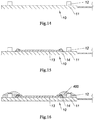
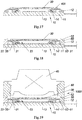
- Figs. 14-19 show the packaging process of the camera module 1000.
- a set of the electronic components 12 are mounted on the circuit board 11.
- the type of the electronic component 12 is not limited in the camera module 1000 according to the present invention.
- the electronic component 12 may be, but not limited to, a resistor, a capacitor, a controller, or the like.
- the photosensitive chip 13 is mounted on the circuit board 11, and at least one set of guiding wires 14 with the two ends being conductively connected to the photosensitive chip 13 and the circuit board 11 respectively are formed by a wire bonding process, so as to form the circuit board assembly 10.
- the stage shown in Fig. 15 may be prior to the stage shown in Fig. 14 , i.e., firstly the photosensitive chip 13 is mounted on the circuit board 11, and then a set of the electronic components 12 are mounted on the circuit board 11 to form the circuit board assembly 10.
- a glue material 400 is applied to the circuit board assembly 10 so that the glue material 400 covers the electronic components 12.
- the glue material 400 applied to the circuit board assembly 10 further extends inward to and wraps the non-photosensitive area 132 of the photosensitive chip 13, and extends outward to and wraps the circuit board 11; and the glue material 400 covers the guiding wires 14.
- the glue material 400 applied to the circuit board assembly 10 has a ring shape, such as a square ring shape, which surrounds the photosensitive area 131 of the photosensitive chip 13.
- the glue material 400 applied to the circuit board assembly 10 covers the highest electronic component 12.
- the glue material 400 applied to the circuit board assembly 10 is the glue material 400 with a relatively high viscosity, so as to avoid an undesirable phenomenon, i.e. prevent the glue material 400 from flowing after being applied to the circuit board assembly 10, thereby avoiding contamination of the photosensitive area 131 of the photosensitive chip 13 during the process of packaging the camera module 1000.
- the light filter 30 is mounted on the top of the glue material 400 applied to the circuit board assembly 10, so that the light filter 30 is kept in the photosensitive path of the photosensitive chip 13 by the glue material 400.
- a force is applied to the light filter 30 in a direction where the photosensitive chip 13 is located, so that a flat surface is formed on the top of the glue material 400 applied to the circuit board assembly 10, and the light filter 30 and the photosensitive area 131 of the photosensitive chip 13 are kept flat.
- the glue material 400 applied to the circuit board assembly 10 is the glue material 400 with a relatively high viscosity, after the light filter 30 is mounted on the top of the glue material 400 applied to the circuit board assembly 10 and the external force applied to the light filter 30 is removed, the relative positions of the light filter 30 and the photosensitive chip 13 will not change.
- the glue material 400 may be applied along a extending direction of the electronic components 12, for example, if the electronic components 12 of the camera module 1000 are in three rows; at this time, the glue material 400 is not applied into a state of surrounding the non-photosensitive area 131 of the photosensitive chip 13, i.e., the glue material 400 is also not applied on a side of the photosensitive chip 13 where the electronic components 12 are not arranged.
- the photosensitive chip 30 is mounted on the top of the glue material 400, a gap will be formed between the light filter 30 and the circuit board assembly 10, and then the gap formed between the light filter 30 and the circuit board assembly 10 may be sealed by replenishing glue or the like.
- the lens holder 50 is mounted on the circuit board 11 of the circuit board assembly 10.
- the lower surface 51 of the lens holder 50 is mounted on the circuit board 11 by the glue material 400, and the inner surface 53 of the lens holder 50 is attached to the glue material 400.
- the glue material 400 applied to the circuit board assembly 10 is cured, so that the bonding portion 20 is formed by the glue material 400 applied to the circuit board assembly 10, and the light filter 30 is kept in the photosensitive path of on the photosensitive chip 13 by the bonding portion 20; wherein a side portion of the glue material 400 bonded to the circuit board assembly 10 forms the lower bonding side 21 of the bonding portion 20, and a side portion of the glue material 400 bonded to the light filter 30 forms the top bonding surface 22; wherein the lower surface 51 of the lens holder 50 is attached to the circuit board 11 by the glue material 400, and the inner surface 53 of the lens holder 50 is bonded to the bonding portion 20.
- the way of curing the glue material 400 applied to the circuit board assembly 10 is not limited and it is selected on the basis of the type of the glue material 400.
- the glue material 400 applied to the circuit board assembly 10 may be cured by heating or ultraviolet light irradiation.
- the top bonding surface 22 of the bonding portion 20 corresponds to the electronic components 12 arranged at the same height, so that a flatness of the top bonding surface 22 of the bonding portion 20 is ensured by the electronic components 12 arranged at the same height, thereby ensuring a flatness of the light filter 30 and the photosensitive area 131 of the photosensitive chip 13.
- the optical lens unit 40 is mounted on the lens bearing portion 60, and the lens bearing portion 60 is mounted on the upper surface 52 of the lens holder 50, so as to keep the optical lens unit 40 in the photosensitive path of the photosensitive chip 13, thereby manufacturing the camera module 1000.
- Fig. 22 shows a modified implementation of the camera module 1000.
- the difference from the camera module 1000 shown in Figs. 14-20 is that: in this specific example of the camera module 1000 shown in Fig. 22 , the camera module 1000 is not provided with the lens bearing portion 60, and the optical lens unit 40 is directly mounted on the lens holder 50, so that the optical lens unit 40 is kept in the photosensitive path of the photosensitive chip 13 by the lens holder 50.
- the optical lens unit 40 is mounted on the lens holder 50, and then the lens holder 50 is mounted on the circuit board 11 of the circuit board assembly 10, finally the glue material 400 applied to the circuit board assembly 10 is cured, so that the bonding portion 20 is formed by the glue material 400 applied to the circuit board assembly 10.
- Fig. 23 shows a modified implementation of the camera module 1000.
- the difference from the camera module 1000 shown in Figs. 14-20 is that: in this specific example of the camera module 1000 shown in Fig. 23 , the glue material 400 is only applied to the circuit board 11 of the circuit board assembly 10, so that after the glue material 400 is cured, the lower bonding side 21 of the bonding portion 20 is only bonded to the circuit board 11 of the circuit board assembly 10.
- Fig. 24 shows a modified implementation of the camera module 1000.
- the difference from the camera module 1000 shown in Figs. 14-20 is that: in this specific example of the camera module 1000 shown in Fig. 24 , the glue material 400 is only applied to the non-photosensitive area 132 of the photosensitive chip 13 of the circuit board assembly 10, so that after the glue material 400 is cured, the lower bonding side 21 of the portion 20 is only bonded to the non-photosensitive area 132 of the photosensitive chip 13 of the circuit board assembly 10.
- the glue material 400 is only applied to the non-photosensitive area 132 of the photosensitive chip 13 of the circuit board assembly 10
- the top bonding surface 22 of the bonding portion 20 corresponds to the non-photosensitive area 132 of the photosensitive chip 13, so that the flatness of the top bonding surface 22 of the bonding portion 20 is ensured by the non-photosensitive area 132 of the photosensitive chip 13, thereby ensuring the flatness of the light filter 30 and the photosensitive area 131 of the photosensitive chip 13.
- Fig. 25 shows a modified implementation of the camera module 1000.
- the difference from the camera module 1000 shown in Figs. 14-20 is that: in this specific example of the camera module 1000 shown in Fig. 25 , the lower surface 51 of the lens holder 50 is mounted on the circuit board 11, and the lens bearing portion 60 is mounted on the upper surface 52 of the lens holder 50, so that the optical lens unit 40 is kept in the photosensitive path of the photosensitive chip 13 by the lens holder 50 and the lens bearing portion 60.
- the glue material 400 applied to the circuit board assembly 10 is cured, so as to form the bonding portion 20 by the glue material 400 applied to the circuit board assembly 10, and then the lower surface 51 of the lens holder 50 is mounted on the circuit board 11, finally the lens bearing portion 60 is mounted on the upper surface 52 of the lens holder 50, so that the optical lens unit 40 is kept in the photosensitive path of the photosensitive chip 13 by the lens bearing portion 60.
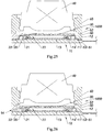
- Fig. 26 shows a modified implementation of the camera module 1000.
- the lens holder 50 further has at least one notch 54 extending from the lower surface 51 to a direction of the upper surface 52, wherein after the lens holder 54 is mounted on the circuit board 11, a part of the glue material 400 applied to the circuit board assembly 10 is accommodated in the notch 54 of the lens holder 50.
- the gap 54 of the lens holder 50 allows the glue material 400 to overflow from the inside of the lens holder 50 to the outside, thereby preventing the glue material 400 from expanding inward and contaminating the photosensitive area 131 of the photosensitive chip 13 or blocking the photosensitive path of the photosensitive chip 13.
- the glue material 400 applied to the circuit board assembly 10 is cured to form the bonding portion 20, a part of the bonding portion 20 is accommodated in the notch 54 of the lens holder 50.
- the notch 54 of the lens holder 50 forms an opening for overflowing glue.
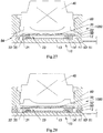
- Fig. 27 shows a modified implementation of the camera module 1000.
- the difference from the camera module 1000 shown in Fig. 26 is that: in this specific example of the camera module 1000 shown in Fig. 27 , the inner surface 53 of the side portion of the lens holder 50 provided with the notch 54 is not mounted on the glue material 400 applied to the circuit board assembly 10, and a gap is reserved between the inner surface 53 of the lens holder 50 and the glue material 400 applied to the circuit board assembly 10.
- the gap 54 of the lens holder 50 allows the air held between the lens holder 50 and the glue material 400 applied to the circuit board assembly 10 to escape, so that the glue material 400 applied to the circuit board assembly 10 is allowed to expand in a direction of the circuit board assembly 10 of the lens holder 50, thereby preventing the glue material 400 from expanding inward and contaminating the photosensitive area 131 of the photosensitive chip 13 or blocking the photosensitive path of the photosensitive chip 13.
- the gap 54 of the lens holder 50 is sealed by the glue material 400 or other materials.
- Fig. 28 shows a modified implementation of the camera module 1000.
- the lens holder 50 is integrally formed on the circuit board 11 and the bonding portion 20.
- the lens holder 50 is formed by a molding process, so that the lower surface 51 of the lens holder 50 is integrally bonded to the circuit board 11, and the inner surface 53 of the lens holder 50 is integrally bonded to the bonding portion 20, thereby manufacturing the camera module 1000 shown in Fig. 28 .
- the present invention further provides a manufacturing method of a camera module 1000, wherein the manufacturing method includes the following steps:
- step (a) further includes the following steps:
- the glue material 400 applied to the circuit board assembly 10 surrounds the photosensitive area 131 of the photosensitive chip 13, so that after the light filter 30 is mounted on the top of the glue material 400, a sealed space is formed between the light filter 30, the glue material 400 and the photosensitive chip 13, and the photosensitive area 131 of the photosensitive chip 13 is kept in the sealed space.
- the glue material 400 applied to the circuit board assembly 10 surrounds the photosensitive area 131 of the photosensitive chip 13, so that after the light filter 30 is mounted on the top of the glue material 400, a sealed space is formed between the light filter 30, the glue material 400 and the photosensitive chip 13, and the photosensitive area 131 of the photosensitive chip 13 is kept in the sealed space.
- the glue material 400 is only applied along an extending direction of the electronic components 12 of the circuit board assembly 10, and after the light filter 30 is mounted on the top of the glue material 400, a gap formed between the light filter 30 and the circuit board assembly 10 is sealed.
- the gap formed between the light filter 30 and the circuit board assembly 10 may be sealed with the glue material 400 by replenishing glue.
- step (a.2) a pressure is applied to the light filter 30 in a direction of the photosensitive chip 13, so that the light filter 30 is mounted on the top of the glue material 400.
- the light filter 30 forms a flat surface on the top of the glue material 400, and at this time, a flatness between the light filter 30 and the photosensitive area 131 of the photosensitive chip 13 may be ensured by the glue material 400, so that after the glue material 400 is cured to form the bonding portion 20, the flatness between the light filter 30 and the photosensitive area 131 of the photosensitive chip 13 may be ensured by the bonding portion 20.
- the step (a) before the step (a.3), further includes the step of: mounting the lens holder 50 on the circuit board 11 of the circuit board assembly 10, so that in the step (a.3), the lower surface 51 of the lens holder 50 is bonded to the circuit board 11, and the inner surface 53 of the lens holder 50 is bonded to the bonding portion 20.
- the packaging relationship between the lens holder 50, the bonding portion 20, and the circuit board assembly 10 may be more reliable.
- the lens holder 50 is provided with the notch 54, so that during the process of curing the glue material 400, the glue material 400 is allowed to overflow from the notch 54 of the lens holder 50, thereby avoiding the undesirable phenomenon of contaminating the photosensitive area 131 of the photosensitive chip 13 or blocking the photosensitive path of the photosensitive chip 13 by the expansion of the glue material 400 in a direction of the photosensitive area 131 of the photosensitive chip 13.
- the inner surface 53 of the side portion of the lens holder 50 provided with the notch 54 is not attached to the glue material 400, so that a gap is formed between the glue material 400 and the inner surface 53 of the lens holder 50, and during the process of curing the glue material 400, the air held between the glue material 400 and the inner surface 53 of the lens holder 50 is allowed to overflows from the notch 54 of the lens holder 50, thereby guiding the glue material 400 to expand in a direction of the inner surface 53 of the lens holder 50.
- step (a) further includes the following steps:
- step (a) further includes the following steps:
Landscapes
- Engineering & Computer Science (AREA)
- Multimedia (AREA)
- Signal Processing (AREA)
- Transforming Light Signals Into Electric Signals (AREA)
- Studio Devices (AREA)
- Blocking Light For Cameras (AREA)
Abstract
Description
- The invention relates to field of optical imaging, in particular to a photosensitive assembly, a camera module, a method for manufacturing the camera module, and an electronic device.
- In recent years, smart devices, such as smart phones, have become increasingly lighter, thinner, and more high-performance. This development trend of smart devices has raised more demanding requirements for the size and imaging capabilities of the camera module, which is one of the standard configurations of smart devices.
- In terms of hardware, the imaging capability of the camera module depends on the number and size of the electronic components in the circuit and the parameters of the photosensitive chip, for example, the size of the photosensitive surface of the photosensitive chip. In other words, the number and size of electronic components and the parameters of the photosensitive chip are the basis for improving the imaging capability of the camera module. However, the existing technology for packaging camera modules has greatly increased the size of camera modules with a greater number and higher size of electronic components and photosensitive chips with better parameters, as a result, the development trend of the size of the high-performance camera modules is contrary to the development trend of the smart devices.
-
Fig. 1 shows a typical camera module in the prior art, which includes acircuit board 1P, a set ofelectronic components 2P, aphotosensitive chip 3P, alens holder 4P, alight filter 5P, a lens bearingportion 6P, and alens unit 7P. Firstly, a set of theelectronic components 2P are mounted on thecircuit board 1P at intervals; secondly, thephotosensitive chip 3P is mounted on thecircuit board 1P, and thephotosensitive chip 3P is conductively connected to thecircuit board 1P through at least one set ofgold wires 8P, wherein a set of theelectronic components 2P surrounds thephotosensitive chip 3P; thirdly, thelens holder 4P is mounted on thecircuit board 1P by surrounding thephotosensitive chip 3P, and a lightfilter bearing arm 41P of thelens holder 4P protrudes from an inner wall of thelens holder 4P, so as to extend toward the direction of the photosensitive path of thephotosensitive chip 3P; fourthly, thelight filter 5P is mounted on the lightfilter bearing arm 41P of thelens holder 4P, so as to maintain thelight filter 5P in the photosensitive path of thephotosensitive chip 3P; fifthly, thelens unit 7P is arranged on the lens bearingportion 6P, and the lens bearingportion 6P is mounted on thelens holder 4P, so as to maintain thelens unit 7P in the photosensitive path of thephotosensitive chip 3P. In the camera module of the prior art, thelight filter 5P needs to be carried by the lightfilter bearing arm 41P of thelens holder 4P. Therefore, thelens holder 4P must be designed to have a structure of the lightfilter bearing arm 41P, and this causes thelens holder 4P to occupy more height space, so that it is difficult to reduce the size in height of the camera module. In addition, in order to prevent the lightfilter bearing arm 41P of thelens holder 4P from contacting with theelectronic component 2P, a space needs to be reserved between the lightfilter bearing arm 41P and theelectronic component 2P, this also makes it difficult to reduce the size in height of the camera module. - An object of the present invention is to provide a photosensitive assembly, a camera module, a method for manufacturing the camera module, and an electronic device, wherein the size in height of the camera module may be reduced, so that the camera module is particularly suitable for being applied to electronic device pursuing thinner and lighter.
- An object of the present invention is to provide a photosensitive assembly, a camera module, a method for manufacturing the camera module, and an electronic device, wherein a light filter of the camera module does not need to be kept in a photosensitive path of a photosensitive chip by being supported by a lens holder, so as to save height space occupied by the lens holder, thereby reducing the size in height of the camera module.
- An object of the present invention is to provide a photosensitive assembly, a camera module, a method for manufacturing the camera module, and an electronic device, wherein a back focus size of the camera module may be reduced to effectively reduce the size in height of the camera module, and particularly, in a preferred example of the camera module according to the present invention, the back focus size of the camera module may be reduced to 0.6 mm or less, thereby effectively reducing the size in height of the camera module.
- An object of the present invention is to provide a photosensitive assembly, a camera module, a method for manufacturing the camera module, and an electronic device, wherein a distance between a mounting surface of a lens bearing portion of the camera module and a lower surface of the light filter may be reduced, so as to effectively reduce the size in height of the camera module, and particularly, in another preferred example of the camera module according to the present invention, the distance between the mounting surface of the lens bearing portion and the lower surface of the light filter may be reduced to 0.2 mm or less, thereby effectively reducing the size in height of the camera module.
- An object of the present invention is to provide a photosensitive assembly, a camera module, a method for manufacturing the camera module, and an electronic device, wherein the camera module provides a bonding portion, and the bonding portion is used to combine the light filter and a circuit board assembly of the camera module, so that the light filter is kept in the photosensitive path of the photosensitive chip by the bonding portion, and in this way, the light filter does not need to be supported by the lens holder.
- An object of the present invention is to provide a photosensitive assembly, a camera module, a method for manufacturing the camera module, and an electronic device, wherein a plane on which a top bonding surface of the bonding portion is located is higher than a plane on which a photosensitive area of the photosensitive chip is located, and a height difference between the two is controlled within a suitable range, and in this way, generation of stray light and imaging of dirty spots may be reduced, thereby improving the imaging quality of the camera module.
- An object of the present invention is to provide a photosensitive assembly, a camera module, a method for manufacturing the camera module, and an electronic device, wherein a width of the bonding portion is controlled within a suitable range, and in this way, packaging tolerances may be compensated, thereby ensuring the reliability of the camera module.
- An object of the present invention is to provide a photosensitive assembly, a camera module, a method for manufacturing the camera module, and an electronic device, wherein the top bonding surface of the bonding portion corresponds to a non-photosensitive area of the photosensitive chip, and in this way, flatness of the top bonding surface of the bonding portion may be ensured, thereby ensuring flatness between the light filter and the photosensitive area of the photosensitive chip.
- An object of the present invention is to provide a photosensitive assembly, a camera module, a method for manufacturing the camera module, and an electronic device, wherein the top bonding surface of the bonding portion corresponds to electronic components arranged at a same height, and in this way, the flatness of the top bonding surface of the bonding portion may be ensured, thereby ensuring the flatness between the light filter and the photosensitive area of the photosensitive chip.
- An object of the present invention is to provide a photosensitive assembly, a camera module, a method for manufacturing the camera module, and an electronic device, wherein the lower surface of the lens holder is bonded to the circuit board, and the inner surface of the lens holder is bonded to the bonding portion, and in this way, the reliability of the camera module may be improved.
- An object of the present invention is to provide a photosensitive assembly, a camera module, a method for manufacturing the camera module, and an electronic device, wherein the lens holder has at least one notch, so that glue material for forming the bonding portion may be discharged from the notch of the lens holder during the process of mounting the lens holder on the circuit board assembly and heating the lens holder, thereby avoiding excessive glue material overflow inward to contaminate the photosensitive area of the photosensitive chip.
- An object of the present invention is to provide a photosensitive assembly, a camera module, a method for manufacturing the camera module, and an electronic device, wherein air between the glue material and the inner surfaces of the lens holder may be discharged from the notch during the process of mounting the lens holder on the circuit board assembly and heating the lens holder, thereby guiding the glue material to expand toward the direction of the inner surface of the lens holder, so as to avoid excessive glue material overflow inward to contaminate the photosensitive area of the photosensitive chip.
- An object of the present invention is to provide a photosensitive assembly, a camera module, a method for manufacturing the camera module, and an electronic device, wherein the camera module is applied to an electronic device, thereby facilitating to increase a screen-to-body ratio of the electronic device.
- An object of the present invention is to provide a photosensitive assembly, a camera module, a method for manufacturing the camera module, and an electronic device, wherein at least one side portion of the camera module forms a retracting portion, and in this way, the camera module may be closer to an edge of an electronic device body, thereby facilitating to increase the screen-to-body ratio of the electronic device.
- According to one aspect of the present invention, the present invention provides a camera module including:
- an optical lens unit;
- a light filter;
- a circuit board assembly, wherein the circuit board assembly includes a circuit board and a photosensitive chip conductively connected to the circuit board; and
- a bonding portion, wherein the bonding portion has a lower bonding side, a top bonding surface, and a light path, and the lower bonding side of the bonding portion is bonded to the circuit board assembly, and the bonding portion surrounds a photosensitive area of the photosensitive chip, so that the photosensitive area of the photosensitive chip is exposed to the light path of the bonding portion, and periphery of the light filter is bonded to the top bonding surface of the bonding portion, so that the light filter is kept in the photosensitive path of the photosensitive chip by the bonding portion, and the optical lens unit is kept in the photosensitive path of the photosensitive chip.
- According to an embodiment of the present invention, the lower bonding side of the bonding portion is bonded to a non-photosensitive area of the photosensitive chip, and the top bonding surface of the bonding portion corresponds to the non-photosensitive area of the photosensitive chip.
- According to an embodiment of the present invention, the lower bonding side of the bonding portion is bonded to the circuit board and the non-photosensitive area of the photosensitive chip, and the top bonding surface of the bonding portion corresponding to the non-photosensitive area of the photosensitive chip.
- According to an embodiment of the present invention, the circuit board assembly further includes a set of electronic components, wherein at least three of the electronic components are arranged at equal heights on and are conductively connected to the circuit board, and the bonding portion embeds the electronic components, and the top bonding surface of the bonding portion corresponds to the electronic components.
- According to an embodiment of the present invention, a plane on which the top bonding surface of the bonding portion is located is lower than a plane on which a top surface of the tallest electronic component is located.
- According to an embodiment of the present invention, a distance between the plane on which the top bonding surface of the bonding portion is located and the plane on which the photosensitive area of the photosensitive chip is located is greater than or equal to 0.15 mm.
- According to an embodiment of the present invention, the bonding portion has four sides, and the adjacent sides are connected end to end and perpendicular to each other to form the light path between the four sides, and a width of at least one side of the bonding portion is greater than or equal to 0.15 mm.
- According to an embodiment of the present invention, the camera module further includes a lens holder, wherein the lens holder has a lower surface, and the lower surface of the lens holder is mounted on the circuit board.
- According to an embodiment of the present invention, the camera module further includes a lens holder, wherein the lens holder has a lower surface, an upper surface corresponding to the lower surface, and an inner surface extending from the upper surface to the lower surface, wherein the lower surface of the lens holder is mounted on the circuit board, and the inner surface of the lens holder is bonded to the bonding portion.
- According to an embodiment of the present invention, the camera module further includes a lens holder, wherein the lens holder has a lower surface, an upper surface corresponding to the lower surface, and an inner surface extending from the upper surface to the lower surface, wherein the lower surface of the lens holder is bonded to the circuit board, and the inner surface of the lens holder is bonded to the bonding portion.
- According to an embodiment of the present invention, the camera module further includes a lens holder, wherein the lens holder has a lower surface, an upper surface corresponding to the lower surface, and an inner surface extending from the upper surface to the lower surface, wherein the lower surface of the lens holder is bonded to the circuit board and the non-photosensitive area of the photosensitive chip, and the inner surface of the lens holder is bonded to the bonding portion.
- According to an embodiment of the present invention, the camera module has four side portions, wherein at least one of the side portions has a side surface, a bottom surface, and a connecting surface connected to the side surface and the bottom surface, and wherein a distance from a connection position of the connecting surface and the side surface to a central axis of the camera module is greater than a distance from a connection position of the connecting surface and the bottom surface to the central axis of the camera module.
- According to an embodiment of the present invention, the connecting surface is an inclined plane; or the connecting surface is a convex arc surface; or the connecting surface is a step surface.
- According to an embodiment of the present invention, the connecting surface is formed on the lens holder and the circuit board.
- According to an embodiment of the present invention, the lens holder has at least one notch extending from the lower surface of the lens holder to a direction of the upper surface, wherein a part of the bonding portion is accommodated in the notch of the lens holder.
- According to an embodiment of the present invention, the camera module further includes a lens bearing portion having a mounting surface, wherein the lens bearing portion is mounted on the lens holder by attaching the mounting surface of the lens bearing portion to the upper surface of the lens holder, and the optical lens unit is arranged on the lens bearing portion.
- According to an embodiment of the present invention, a range of value of a distance parameter D between the mounting surface of the lens bearing portion and the lower surface of the light filter is: 0.1mm≤D≤0.2 mm.
- According to an embodiment of the present invention, a range of value of a back focal length parameter L of the camera module is: 0.4mm≤L≤0.6mm, wherein the back focal length of the camera module refers to a distance between a lower surface of a lens of the optical lens unit close to the photosensitive chip and the photosensitive area of the photosensitive chip.
- According to another aspect of the present invention, the present invention further provides an electronic device, which includes an electronic device body and at least one camera module arranged in the electronic device body, wherein the camera module includes:
- an optical lens unit;
- a light filter;
- a circuit board assembly, wherein the circuit board assembly includes a circuit board and a photosensitive chip conductively connected to the circuit board; and
- a bonding portion, wherein the bonding portion has a lower bonding side, a top bonding surface, and a light path, wherein the lower bonding side of the bonding portion is bonded to the circuit board assembly, and the bonding portion surrounds a photosensitive area of the photosensitive chip, so that the photosensitive area of the photosensitive chip is exposed to the light path of the bonding portion, and periphery of the light filter is bonded to the top bonding surface of the bonding portion, so that the light filter is kept in the photosensitive path of the photosensitive chip by the bonding portion, and the optical lens unit is kept in the photosensitive path of the photosensitive chip.
- According to another aspect of the present invention, the present invention further provides a photosensitive assembly including:
- a light filter;
- a circuit board assembly, wherein the circuit board assembly includes a circuit board and a photosensitive chip conductively connected to the circuit board; and
- a bonding portion, wherein the bonding portion has a lower bonding side, a top bonding surface, and a light path, wherein the lower bonding side of the bonding portion is bonded to the circuit board assembly, and the bonding portion surrounds a photosensitive area of the photosensitive chip, so that the photosensitive area of the photosensitive chip is exposed to the light path of the bonding portion, and periphery of the light filter is bonded to the top bonding surface of the bonding portion, so that the light filter is kept in the photosensitive path of the photosensitive chip by the bonding portion.
- According to an embodiment of the present invention, the lower bonding side of the bonding portion is bonded to the non-photosensitive area of the photosensitive chip, and the top bonding surface of the bonding portion corresponds to the non-photosensitive area of the photosensitive chip.
- According to an embodiment of the present invention, the lower bonding side of the bonding portion is bonded to the circuit board and the non-photosensitive area of the photosensitive chip, and the top bonding surface of the bonding portion corresponds to the non-photosensitive area of the photosensitive chip.
- According to an embodiment of the present invention, the circuit board assembly further includes a set of electronic components, wherein at least three of the electronic components are arranged at equal heights on and are conductively connected to the circuit board, and the bonding portion embeds the electronic components, and the top bonding surface of the bonding portion corresponds to the electronic components.
- According to an embodiment of the present invention, a plane on which the top bonding surface of the bonding portion is located is lower than a plane on which a top surface of the tallest electronic component is located.
- According to an embodiment of the present invention, a distance between the plane on which the top bonding surface of the bonding portion is located and the plane on which the photosensitive area of the photosensitive chip is located is greater than or equal to 0.15 mm.
- According to an embodiment of the present invention, the bonding portion has four sides, and the adjacent sides are connected end to end and perpendicular to each other to form the light path between the four sides, and a width of at least one side of the bonding portion is greater than or equal to 0.15 mm.
- According to one aspect of the present invention, the present invention provides a method for manufacturing a camera module, wherein the manufacturing method includes the following steps:
- (a) respectively bonding a lower bonding side of a bonding portion to a circuit board assembly and bonding a light filter to a top bonding surface of the bonding portion, so as to keep the light filter in a photosensitive path of a photosensitive chip of the circuit board assembly; and
- (b) keeping an optical lens unit in the photosensitive path of the photosensitive chip to manufacture the camera module.
- According to an embodiment of the present invention, the step (a) further includes the following steps:
- (a.1) applying glue material to the circuit board assembly around a photosensitive area of the photosensitive chip;
- (a.2) mounting the light filter on the top of the glue material; and
- (a.3) curing the glue material to form the bonding portion, wherein a side portion of the glue material bonded to the circuit board assembly forms the lower bonding side of the bonding portion, and a side portion of the glue material bonded to the light filter forms the top bonding surface of the bonding portion.
- According to an embodiment of the present invention, in the step (a.2), pressure is applied to the light filter in a direction towards the photosensitive chip, so as to mount the light filter on the top of the glue material.
- According to an embodiment of the present invention, before the step (a.3), the step (a) further includes the step of: mounting a lens holder on a circuit board of the circuit board assembly, so that in the step (a.3), the lower surface of the lens holder is bonded to the circuit board, and the inner surface of the lens holder is bonded to the bonding portion.
- According to an embodiment of the present invention, in the step (a.3), the glue material is configured to overflow from a notch of the lens holder.
- According to an embodiment of the present invention, in the step (a.3), the glue material is guided to expand toward a direction of the inner surface of the lens holder.
- According to an embodiment of the present invention, in the above method, air held between the glue material and the inner surface of the lens holder is allowed to escape from a notch of the lens holder, thereby guiding the glue material to expand toward the direction of the inner surface of the lens holder.
- According to an embodiment of the present invention, in the step (a.1), a glue material is applied to a non-photosensitive area of the photosensitive chip, so that in the step (a.3), the top bonding surface of the bonding portion corresponds to the non-photosensitive area of the photosensitive chip.
- According to an embodiment of the present invention, in the step (a.1), a glue material is configured to cover at least three electronic components which are arranged at the same height and conductively connected to a circuit board of the circuit board assembly; so that in the step (a.3), the top bonding surface of the bonding portion corresponds to the electronic components.
- According to an embodiment of the present invention, in the step (a.1), a glue material is configured to cover at least three electronic components which are arranged at the same height and conductively connected to a circuit board; so that in the step (a.3), the top bonding surface of the bonding portion corresponds to the electronic components.
- According to an embodiment of the present invention, in the step (a.1), a glue material is applied to the circuit board assembly along an extension direction of a set of electronic components of the circuit board, and before the step (a.2) and the step (a.3), a gap formed between the light filter and the circuit board assembly is sealed.
- According to an embodiment of the present invention, the step (a) further includes the following steps:
- (a.1') forming a ring-shaped boss on peripheral edges of the light filter;
- (a.2') mounting the ring-shaped boss on the non-photosensitive area of the photosensitive chip; and
- (a.3') curing the ring-shaped boss to form the bonding portion, wherein a side portion of the ring-shaped boss bonded to the non-photosensitive area of the photosensitive chip forms the lower bonding side of the bonding portion, and a side portion of the ring-shaped boss bonded to the light filter forms the top bonding surface of the bonding portion.
- According to an embodiment of the present invention, a distance between a plane on which the top bonding surface of the bonding portion is located and a plane on which the photosensitive area of the photosensitive chip is located is greater than or equal to 0.15 mm.
- According to an embodiment of the present invention, the bonding portion has four sides, and the adjacent sides are connected end to end and perpendicular to each other to form the light path between the four sides, wherein a width of at least one of the side edges of the bonding portion is greater than or equal to 0.15 mm.
- According to an embodiment of the present invention, in the step (a.2'), the ring-shaped boss is mounted on the non-photosensitive area of the photosensitive chip by glue.
- According to an embodiment of the present invention, the step (a) further includes the following steps:
- (a.1") forming a ring-shaped boss on the non-photosensitive area of the photosensitive chip;
- (a.2") mounting peripheral edges of the light filter on the ring-shaped boss; and
- (a.3") curing the ring-shaped boss to form the bonding portion, wherein a side portion of the ring-shaped boss bonded to the non-photosensitive area of the photosensitive chip forms the lower bonding side of the bonding portion, and a side portion of the ring-shaped boss bonded to the light filter forms the top bonding surface of the bonding portion.
- According to an embodiment of the present invention, in the step (a.2"), the light filter is mounted on the ring-shaped boss by glue.
- According to an embodiment of the present invention, after the step (a), the manufacturing method further includes the step of: mounting a lens holder on a circuit board of the circuit board assembly, so that in the step (c), the optical lens unit is kept in the photosensitive path of the photosensitive chip by the lens holder.
- According to an embodiment of the present invention, after the step (a), the manufacturing method further includes the step of: forming a lens holder on a circuit board of the circuit board assembly, so that in the step (c), the optical lens unit is kept in the photosensitive path of the photosensitive chip by the lens holder.
- According to an embodiment of the present invention, after the step (c), the manufacturing method further includes the step of: removing a part of at least one side portion of the camera module, so that the side portion forms a side surface, a bottom surface, and a connecting surface connected to the side surface and the bottom surface, wherein a distance from a connection position of the connecting surface and the side surface to a central axis of the camera module is greater than a distance from a connection position of the connecting surface and the bottom surface to the central axis of the camera module.
- According to an embodiment of the present invention, in the above method, the side portion of the camera module is cut, so that the side portion forms the side surface, the bottom surface, and the connecting surface connected to the side surface and the bottom surface.
- According to an embodiment of the present invention, in the above method, the side portion of the camera module is ground, so that the side portion forms the side surface, the bottom surface, and the connecting surface connected to the side surface and the bottom surface.
-
-
Fig. 1 is a schematic diagram of a camera module in the prior art. -
Fig. 2 is a schematic sectional view of the first manufacturing processes of a camera module according to the first preferred embodiment of the present invention. -
Fig. 3 is a schematic sectional view of the second manufacturing process of the camera module according to the above preferred embodiment of the present invention. -
Fig. 4 is a three-dimensional schematic diagram of the third manufacturing process of the camera module according to the above preferred embodiment of the present invention. -
Fig. 5 is a schematic sectional view of the fourth manufacturing process of the camera module according to the above preferred embodiment of the present invention. -
Fig. 6 is a schematic sectional view of the fifth manufacturing process of the camera module according to the above preferred embodiment of the present invention. -
Fig. 7 is a schematic sectional view of the sixth manufacturing process of the camera module according to the above preferred embodiment of the present invention, which shows a sectional state of the camera module after being cut along a middle position. -
Fig. 8 is a three-dimensional schematic diagram of the camera module according to the above preferred embodiment of the present invention. -
Fig. 9 is a three-dimensional schematic diagram of an application state of the camera module according to the above preferred embodiment of the present invention. -
Fig. 10 is a schematic sectional view of a modified implementation of the camera module, according to the above preferred embodiment of the present invention. -
Fig. 11A is a schematic sectional view of an application state of the camera module according to the above preferred embodiment of the present invention. -
Fig. 11B is a sectional view of an application state of the camera module in the prior art. -
Figs. 12A-12C are schematic diagrams of different states of a relationship between the camera module and a housing of an electronic device body according to the above preferred embodiment of the present invention. -
Fig. 13 is a schematic sectional view of another modified implementation of the camera module according to the above preferred embodiment of the present invention. -
Fig. 14 is a schematic sectional view of the first manufacturing processes of a camera module according to the second preferred embodiment of the present invention. -
Fig. 15 is a schematic sectional view of the second manufacturing process of the camera module according to the above preferred embodiment of the present invention. -
Fig. 16 is a schematic sectional view of the third manufacturing process of the camera module according to the above preferred embodiment of the present invention. -
Fig. 17 is a schematic sectional view of the fourth manufacturing process of the camera module according to the above preferred embodiment of the present invention. -
Fig. 18 is a schematic sectional view of the fifth manufacturing process of the camera module according to the above preferred embodiment of the present invention. -
Fig. 19 is a schematic sectional view of the sixth manufacturing process of the camera module according to the above preferred embodiment of the present invention, which shows a sectional view state of the camera module after being cut along a middle position. -
Fig. 20 is a three-dimensional schematic diagram of the camera module according to the above preferred embodiment of the present invention. -
Fig. 21 is a schematic sectional view of a first modified implementation of the camera module according to the above preferred embodiment of the present invention. -
Fig. 22 is a schematic sectional view of a second modified implementation of the camera module according to the above preferred embodiment of the present invention. -
Fig. 23 is a schematic sectional view of a third modified implementation of the camera module according to the above preferred embodiment of the present invention. -
Fig. 24 is a schematic sectional view of a fourth modified implementation of the camera module according to the above preferred embodiment of the present invention. -
Fig. 25 is a schematic sectional view of a fourth modified implementation of the camera module according to the above preferred embodiment of the present invention. -
Fig. 26 is a schematic sectional view of a third modified implementation of the camera module according to the above preferred embodiment of the present invention. -
Fig. 27 is a schematic sectional view of a fourth modified implementation of the camera module according to the above preferred embodiment of the present invention. -
Fig. 28 is a schematic sectional view of a fourth modified implementation of the camera module according to the above preferred embodiment of the present invention. - The following description is used to disclose the present invention so that those skilled in the art may implement the present invention. The preferred embodiments in the following description are only examples, and those skilled in the art may think of other obvious variations. The basic principles of the present invention defined in the following description may be applied to other embodiments, modifications, improvements, equivalents, and other technical solutions that do not deviate from the spirit and scope of the present invention.
- Those skilled in the art should understand that in the disclosure of the present invention, the orientation or positional relationship indicated by the terms "longitudinal", "lateral", "upper", "lower", "front", "rear", "left", "right", "vertical", "horizontal", "top", "bottom", "inner", "outer", etc. " are based on an orientation or positional relationship shown in the drawings, which is only for the convenience of describing the present invention and simplifying the description, rather than indicating or implying that the device or element referred to must have a specific orientation, be constructed and operated in a specific orientation, and therefore the above-mentioned terms should not be construed as limiting the present invention.
- It may be understood that the term "a/an" should be understood as "at least one" or "one or more", i.e., in one embodiment, the number of an element may be one, and in another embodiment, the number of the element may be more than one, and the term "one" cannot be understood as a restriction on the number.
- Referring to
Figs. 2-8 of the accompanying drawings of the specification of the present invention, acamera module 1000 according to the first preferred embodiment of the present invention is disclosed and explained in the following description, wherein thecamera module 1000 includes acircuit board assembly 10, abonding portion 20, alight filter 30, and anoptical lens unit 40. - Referring to
Figs. 7-8 , thecircuit board assembly 10 includes acircuit board 11 and a set ofelectronic components 12 conductively connected to thecircuit board 11, and there is a gap between the adjacentelectronic components 12. The manner of conductively connecting theelectronic component 12 to thecircuit board 11 is not limited. For example, in the specific example of thecamera module 1000 shown inFigs. 7-8 , theelectronic component 12 is conductively connected to thecircuit board 11 by being mounted on the surface of thecircuit board 11. Optionally, theelectronic component 12 is conductively connected to thecircuit board 11 in such a manner that at least a part of it is embedded inside of thecircuit board 11. - Further referring to
Figs. 7-8 , thecircuit board assembly 10 further includes aphotosensitive chip 13, which has aphotosensitive area 131 and anon-sensitive area 132 surrounding thephotosensitive area 131, wherein thephotosensitive chip 13 is conductively connected to thecircuit board 11. The manner of conductively connecting thephotosensitive chip 13 to thecircuit board 11 is not limited. For example, in the specific example of thecamera module 1000 shown inFigs. 7-8 , thephotosensitive chip 13 is mounted on the surface of thecircuit board 11, and two ends of at least one set of guidingwires 14 formed by a wire bonding process are conductively connected to thephotosensitive chip 13 and thecircuit board 11, respectively, so that thephotosensitive chip 13 is conductively connected to thecircuit board 11. Optionally, thephotosensitive chip 13 is mounted on thecircuit board 11 and conductively connected to thecircuit board 11 by a flip-chip process. - Particularly, in the
camera module 1000 shown inFigs. 7-8 , a set of theelectronic components 12 form two rows of theelectronic components 12, wherein one row of theelectronic components 12 are located on the left side of thephotosensitive chip 13, another row of theelectronic components 12 are located on the right side of thephotosensitive chip 13. Optionally, a set of theelectronic components 12 form three rows of theelectronic components 12, wherein the three rows of theelectronic components 12 are respectively located on three sides of thephotosensitive chip 13. Optionally, a set of theelectronic components 12 form four rows of theelectronic components 12, wherein the four rows of theelectronic components 12 are located on four sides of thephotosensitive chip 13. Optionally, more than two rows of theelectronic components 12 may also be arranged on a same side of thephotosensitive chip 13. Therefore, the relative arrangement of theelectronic components 12 and thephotosensitive chip 13 shown inFigs. 2-7 are only for reference, and should not be regarded as a limitation to the content and scope of thecamera module 1000 of the present invention. - The
bonding portion 20 is ring-shaped and has alower bonding side 21, atop bonding surface 22 corresponding to thelower bonding side 21, and alight path 23 extending from thetop bonding surface 22 to thelower bonding side 21. Thelower bonding side 21 of thebonding portion 20 is bonded to thecircuit board assembly 10, and thebonding portion 20 surrounds thephotosensitive area 131 of thephotosensitive chip 13; a plane on which thetop bonding surface 22 of thebonding portion 20 is located is higher than a plane on which thephotosensitive area 131 of thephotosensitive chip 13 is located, and thephotosensitive area 131 of thephotosensitive chip 13 corresponds to thelight path 23 of thebonding portion 20. Periphery of thelight filter 30 is bonded to thetop bonding surface 22 of thebonding portion 20, so that thelight filter 30 is kept in the photosensitive path of thephotosensitive chip 13. Theoptical lens unit 40 is kept in the photosensitive path of thephotosensitive chip 13. In this preferred example of thecamera module 1000 of the present invention shown inFigs. 7-8 , thebonding portion 20 is in a shape of a square ring, i.e., thebonding portion 20 has foursides 24, wherein twoadjacent sides 24 are connected end to end and perpendicular to each other, so that thelight path 23 is formed between thebonding portions 20 formed by the foursides 24. Eachside 24 of thebonding portion 20 is respectively located outside thephotosensitive area 131 of thephotosensitive chip 13. - Preferably, the
lower bonding side 21 of thebonding portion 20 is bonded to thenon-photosensitive area 132 of thephotosensitive chip 13, and thebonding portion 20 extends upward from thenon-photosensitive area 132 of thephotosensitive chip 13 to a suitable height, and forms thetop bonding surface 22 of thebonding portion 20; and thetop bonding surface 22 of thebonding portion 20 corresponds to thenon-photosensitive area 132 of thephotosensitive chip 13; in this way, a flatness of thetop bonding surface 22 of thebonding portion 20 may be ensured by thenon-photosensitive area 132 of thephotosensitive chip 13, thereby ensuring the flatness between thelight filter 30 and thephotosensitive area 131 of thephotosensitive chip 13. - A distance size (parameter H) between the plane on which the
top bonding surface 22 of thebonding portion 20 is located and the plane on which thephotosensitive area 131 of thephotosensitive chip 13 is located is greater than or equal to 0.15 mm. In this way, it is beneficial for reducing generation of stray light and imaging of dirty spots, thereby improving the imaging quality of thecamera module 1000. - A width size (parameter W) of the
side 24 of thebonding portion 20 is greater than or equal to 0.15mm. In this way, packaging tolerances may be compensated, so that thelight filter 30 is reliably supported in the photosensitive path of thephotosensitive chip 13 by thebonding portion 20. - In the present invention, the
circuit board assembly 10, thebonding portion 20, and thelight filter 30 form a photosensitive assembly, i.e., thecamera module 1000 includes the photosensitive assembly and theoptical lens unit 40 which is kept in the photosensitive path of thephotosensitive chip 13, and the light entering the inside of thecamera module 1000 from theoptical lens unit 40 may be received by thephotosensitive chip 13 and photo-electrically converted. - Further to refer to
Figs. 7-8 , thecamera module 1000 further includes alens holder 50 and alens bearing portion 60 mounted on thelens holder 50. Thelens holder 50 has alower surface 51, anupper surface 52 corresponding to thelower surface 51, and aninner surface 53 extending from theupper surface 52 to thelower surface 51. Thelower surface 51 of thelens holder 50 is integrally bonded to thecircuit board 11 and thenon-photosensitive area 132 of thephotosensitive chip 13, and theinner surface 53 of thelens holder 50 is integrally bonded to thebonding portion 20. Theoptical lens unit 40 is arranged on thelens bearing portion 60, and thelens bearing portion 60 has a mountingsurface 61, wherein thelens bearing portion 60 is mounted on thelens holder 50 in such a manner that the mountingsurface 61 of thelens bearing portion 60 is mounted on theupper surface 52 of thelens holder 50, so that theoptical lens unit 40 is kept in the photosensitive path of thephotosensitive chip 13 by thelens holder 50 and thelens bearing portion 60. - The type of the
lens bearing portion 60 is selected according to the type of thecamera module 1000. For example, when thecamera module 1000 is a fixed-focus camera module, thelens bearing portion 60 is selected as a lens barrel. Correspondingly, when thecamera module 1000 is a zoom camera module, thelens bearing portion 60 is selected as a motor, such as but not limited to a voice coil motor. - Referring to
Fig. 7 , preferably, a parameter of a distance between the mountingsurface 61 of thelens bearing portion 60 and the lower surface of thelight filter 30 is set as D, and a range of value of the parameter D is 0.1-0.2mm (including 0.1mm and 0.2mm) to help reduce the size in height of thecamera module 1000. It is worth mentioning that, in thecamera module 1000 of the present invention, thelight filter 30 is kept in the photosensitive path of thephotosensitive chip 13 by thebonding portion 20, and thelens bearing portion 60 is mounted on thelens holder 50, so that compared to the camera module in prior art, in this preferred example of thecamera module 1000 of the present invention, the distance between the mountingsurface 61 of thelens bearing portion 60 and the lower surfaces of thelight filter 30 may be smaller, which is particularly important for reducing the size in height of thecamera module 1000. - Further referring to
Fig. 7 , in this preferred example of thecamera module 1000 according to the present invention, thelight filter 30 is kept in the photosensitive path of thephotosensitive chip 13 by thebonding portion 20, and thelens bearing portion 60 is mounted on thelens holder 50 so that theoptical lens unit 40 is kept in the photosensitive path of thephotosensitive chip 13 by thelens bearing portion 60 and thelens holder 50. Since thelens holder 50 does not need to keep thelight filter 30 in the photosensitive path of thephotosensitive chip 13, a height of theupper surface 52 of the lens holder 50 (the distance from theupper surface 52 to the photosensitive chip 13) may be reduced, thereby reducing a distance between theoptical lens unit 40 and thephotosensitive area 131 of thephotosensitive chip 13. In this way, a back focus size of thecamera module 1000 may be reduced, thereby facilitating to reduce the size in height of thecamera module 1000. The back focal length of thecamera module 1000 refers to a distance between a surface of a lens of theoptical lens unit 40 which is closest to thephotosensitive chip 13 and thephotosensitive area 131 of thephotosensitive chip 13. A parameter of the back focal length of thecamera module 1000 is set as L, wherein a range of value of the parameter L is 0.4-0.6mm (including 0.4mm and 0.6mm), as compared with the back focal length of 0.8mm in the camera module of prior art, the back focal length of thecamera module 1000 according to the present invention may be reduced by a large value, thereby facilitating to reduce the size in height of thecamera module 1000. - Optionally, in an example of the
camera module 1000, thelens bearing portion 60 and thelens holder 50 may be an integrated structure. In another example of thecamera module 1000, thecamera module 1000 may not be configured with thelens bearing portion 60. In this case, thecamera module 1000 keeps theoptical lens unit 40 in the photosensitive path of thephotosensitive chip 13 by directly mounting theoptical lens unit 40 on thelens holder 50. - In the
camera module 1000 shown inFigs. 7-8 , thelens holder 50 is not prefabricated, wherein thelens holder 50 may be integrally formed by a molding process and bonded to thecircuit board assembly 10 and thebonding portion 20, thereby allowing thelower surface 51 of thelens holder 50 to be integrally bonded to thecircuit board 11 and thenon-photosensitive area 132 of thephotosensitive chip 13, and allowing theinner surface 53 of thelens holder 50 to be integrally bonded to thebonding portion 20. In this way, the reliability for bonding thelens holder 50 to thecircuit board 11, thephotosensitive chip 13, and thebonding portion 20 is higher, thereby facilitating to ensure the stability and reliability of thecamera module 1000. Optionally, thelens holder 50 may be further integrally bonded to the peripheral edges of thelight filter 30. - The
camera module 1000 adopts a manner in which thelens holder 50 is integrally bonded to thecircuit board 11 and thenon-photosensitive area 132 of thephotosensitive chip 13, so that the packaging process of thecamera module 1000 no longer requires thelens holder 50 to be prefabricated, thereby facilitating to reduce the cost and risk of the management and control of the components of thecamera module 1000. - The
camera module 1000 adopts a manner in which thelens holder 50 is integrally bonded to thecircuit board 11 and thenon-photosensitive area 132 of thephotosensitive chip 13; this is not only beneficial to ensure the reliability of the bonding relationship of thecircuit board 11 and thephotosensitive chip 13, and the flatness of thephotosensitive chip 13 is no longer limited by the flatness of thecircuit board 11; wherein the flatness of thephotosensitive chip 13 is ensured by thelens holder 50, thereby facilitating to ensure the flatness of thephotosensitive chip 13. Particularly, in such a manner that thelens holder 50 is integrally bonded to thecircuit board 11 and thenon-photosensitive area 132 of thephotosensitive chip 13 through a molding die, the top surface of thelens holder 50 may be made flatter and is not affected by the inclination or deformation of thecircuit board 11, so as to reduce cumulative tolerances during the subsequent assembly; in this way, it is beneficial to ensure the coaxiality of theoptical lens unit 40 and thephotosensitive chip 13. - The
camera module 1000 adopts a manner in which thelens holder 50 is integrally bonded to thecircuit board 11 and thenon-photosensitive area 132 of thephotosensitive chip 13, so that thelens holder 50 ensures the flatness of thephotosensitive chip 13; in this way, a thinner size may be selected for thecircuit board 11, thereby facilitating to reduce the size in height of thecamera module 1000. Particularly, in such a manner that thelens holder 50 is integrally bonded to thecircuit board 11 through a molding process, thelens holder 50 may reinforce thecircuit board 11, so that thecircuit board 11 may be thinner under the premise of ensuring the flatness of thecircuit board 11, and this is beneficial to reduce the overall size in height of thecamera module 1000. - The
camera module 1000 adopts the manner in which thelens holder 50 is integrally bonded to thecircuit board 11 and thenon-photosensitive area 132 of thephotosensitive chip 13, and this may avoid using glue to mount thelens holder 50 on thecircuit board 11, thereby facilitating to reduce the height size of thecamera module 1000. - Referring to
Fig. 7 , thecamera module 1000 adopts a manner in which thelight filter 30 is kept in the photosensitive path of thephotosensitive chip 13 by thebonding portion 20. On one hand, the cost of thecamera module 1000 may be reduced by reducing the size of thelight filter 30; on the other hand, the lower surface of the light filter 30 (the surface of thelight filter 30 facing the photosensitive chip 13) may be lower than the height of the top surface of the highestelectronic component 12. In this way, in conjunction with the improvement in the optical design of thecamera module 1000, and after reducing the back focus of thecamera module 1000, thelight filter 30 of thecamera module 1000 may be closer to thephotosensitive chip 13, so that theoptical lens unit 40 has the possibility of being adjusted toward the direction of thephotosensitive chip 13, thereby facilitating to reduce the height size of thecamera module 1000. -
Figs. 2-7 show the packaging process of thecamera module 1000. - Referring to
Fig. 2 , a set of theelectronic components 12 are mounted on thecircuit board 11. The type of theelectronic component 12 is not limited in thecamera module 1000 of the present invention. For example, theelectronic component 12 may be, but not limited to, a resistor, a capacitor, a controller, and the like. - Referring to
Fig. 3 , thephotosensitive chip 13 is mounted on thecircuit board 11, and at least one set of guidingwires 14 with the two ends being conductively connected to thephotosensitive chip 13 and thecircuit board 11 respectively are formed by a wire bonding process, so as to form thecircuit board assembly 10. - It is worth mentioning that, the stage shown in
Fig. 3 may be prior to the stage shown inFig. 2 , i.e., firstly thephotosensitive chip 13 is mounted on thecircuit board 11, and then a set of theelectronic components 12 are mounted on thecircuit board 11 to form thecircuit board assembly 10. - Referring to
Fig. 4 , a ring-shapedboss 200 is formed around one side portion of thelight filter 30, so as to form alight filter 300 with a ring-shaped boss. For example, in the preferred example of thecamera module 1000 shown inFigs. 7-8 , the ring-shapedboss 200 may be formed around one side portion of thelight filter 30 through a screen printing process, so as to form thelight filter 300 with the ring-shaped boss. Optionally, the ring-shapedboss 200 may also be formed around one side portion of thelight filter 30 through a photolithography process, so as to form thelight filter 300 with the ring-shaped boss. The material for forming the ring-shapedboss 200 may be, but is not limited to, colloid. - It is worth mentioning that, the sequence of forming the
circuit board assembly 10 and forming thelight filter 300 with the ring-shaped boss is not limited. - Referring to
Fig. 5 , firstly, the light filter 300 with the ring-shaped boss is mounted on the circuit board assembly 10, wherein the ring-shaped boss 200 is mounted on the non-photosensitive area 132 of the photosensitive chip 13; for example, in an example, if the material of the ring-shaped boss 200 is a colloidal material, the ring-shaped boss 200 may be directly mounted on the non-photosensitive area 132 of the photosensitive chip 13; in another example, if the material of the ring-shaped boss 200 is non-colloid, it is necessary to mount the ring-shaped boss 200 on the non-photosensitive area 132 of the photosensitive chip 13 by glue or a similar substance; secondly, the ring-shaped boss 200 is cured, so that the ring-shaped boss 200 forms the bonding portion 20, and the light filter 30 is kept in the photosensitive path of the photosensitive chip 13 by the bonding portion 20, wherein the surface of the ring-shaped boss 200 bonded to the photosensitive chip 13 forms the lower bonding side 21 of the bonding portion 20, and the surface of the ring-shaped boss 200 bonded to the light filter 30 forms the top bonding surface 22 of the bonding portion 20, and a hollow portion in the middle of the ring-shaped boss 200 forms the light path 23 of the bonding portion 20. - It is worth mentioning that, the way of curing the ring-shaped
boss 200 is not limited, and it is selected according to the material for forming the ring-shapedboss 200. For example, the ring-shapedboss 200 may be cured by heating or irradiation with ultraviolet light, so as to form thebonding portion 20. - Referring to
Fig. 6 , thelens holder 50 is formed on thecircuit board assembly 10 and thebonding portion 20 through a molding process, so that thelower surface 51 of thelens holder 50 is integrally bonded to thecircuit board 11 and thephotosensitive chip 13 of thecircuit board assembly 10, and theinner surface 53 of thelens holder 50 is integrally bonded to thebonding portion 20. Preferably, thelens holder 50 embeds theelectronic components 12 and the guidingwires 14 protruding from thecircuit board 11; in this way, firstly, there is no need to reserve a safe space between thelens holder 50 and theelectronic components 12, thereby facilitating to reduce the height size of thecamera module 1000; secondly, thelens holder 50 prevents theelectronic components 12 from being exposed, thereby preventing the pollutants such as debris falling off the surface of theelectronic components 12 from contaminating otherelectronic components 12 or contaminating thephotosensitive chip 13; thirdly, theupper surface 52 of thelens holder 50 has a higher flatness, so that after theoptical lens unit 40 is kept in the photosensitive path of thephotosensitive chip 13 by mounting thelens bearing portion 60 on theupper surface 52 of thelens holder 50, the central axis of theoptical lens unit 40 and the central axis of thephotosensitive area 131 of thephotosensitive chip 13 may be overlapped, so as to ensure the imaging quality of thecamera module 1000; fourthly, thelens holder 50 may be filled in the space between the adjacentelectronic components 12, so as to isolate the adjacentelectronic components 12 and prevent the adjacentelectronic components 12 from interfering with each other. In this way, a distance between the adjacentelectronic components 12 may be smaller, so that thecamera module 1000 may be equipped with a larger number and larger size of theelectronic components 12. - Referring to
Figs. 7-8 , theoptical lens unit 40 is mounted on thelens bearing portion 60, and thelens bearing portion 60 is mounted on theupper surface 52 of thelens holder 50, so as to keep theoptical lens unit 40 in the photosensitive path of thephotosensitive chip 13, thereby manufacturing thecamera module 1000. - Optionally, in another manufacturing process of the
camera module 1000, firstly, the ring-shapedboss 200 is formed in thenon-photosensitive area 132 of thephotosensitive chip 13 by a screen printing process or a photolithography process; secondly, thelight filter 30 is mounted on the ring-shapedboss 200, for example, glue or similar substance may be used to mount thelight filter 30 on the ring-shapedboss 200; then, the ring-shapedboss 200 is cured, so that the ring-shapedboss 200 forms thebonding portion 20, and thelight filter 30 is kept in the photosensitive path of thephotosensitive chip 13 by thebonding portion 20, wherein a surface for bonding the ring-shapedboss 200 to thephotosensitive chip 13 forms thelower bonding side 21 of thebonding portion 20, a surface for bonding the ring-shapedboss 200 to thelight filter 30 forms thetop bonding surface 22 of thebonding portion 20, and the hollow portion in the middle of the ring-shapedboss 200 forms thelight path 23 of thebonding portion 20. -
Fig. 9 shows an application state of thecamera module 1000, wherein thecamera module 1000 is arranged in anelectronic device body 2000, so that theelectronic device body 2000 and thecamera module 1000 form an electronic device. It is worth mentioning that, the example in which the electronic device is a smart phone shown inFig. 9 is only an example, which does not limit the application scope of thecamera module 1000 according to the present invention. For example, the types of the electronic device may be, but are not limited to, a tablet computer, a notebook computer, a personal digital assistant, and a MP3/4/5. -
Fig. 10 shows a modified implementation of thecamera module 1000, andFig. 11A shows an application state of thecamera module 1000. The difference from thecamera module 1000 shown inFigs. 7-8 is that: in this specific example of thecamera module 1000 shown inFig. 10 , thecamera module 1000 has fourside portions 101, wherein at least oneside portion 101 of thecamera module 1000 further has a side surface 1011, a bottom surface 1012, and a connecting surface 1013 connected to the side surface 1011 and the bottom surface 1012, and wherein a distance L1 from a connection position of the side surface 1011 and the connecting surface 1013 to a central axis of thecamera module 1000 is greater than a distance L2 from a connection position of the bottom surface 1012 and the connecting surface 1013 to the central axis of thecamera module 1000, so that at least oneside portion 101 of thecamera module 1000 has a retracting portion, so as to match a turning part of a housing of the electronic device body; in this way, theoptical lens unit 40 of thecamera module 1000 may be closer to the edge of thehousing 2001 of theelectronic device body 2000, thereby facilitating to increase the screen-to-body ratio of the electronic device. Particularly, comparing to the relationship between the camera module and the housing of the electronic device in the prior art shown inFig. 11B , it can be seen that the distance between thecamera module 1000 of the present invention and the edge of thehousing 2001 of theelectronic device body 2000 is smaller, thereby facilitating to increase the screen-to-body ratio of the electronic device. -
Fig. 12A shows a relationship between thecamera module 1000 and thehousing 2001 of theelectronic device body 2000 after thecamera module 1000 is arranged in the electronic device body to form the electronic device, wherein aside portion 101 with a locking portion of thecamera module 1000 corresponds to the turning part of thehousing 2001 of theelectronic device body 2000, so that theoptical lens unit 40 of thecamera module 1000 may be closer to the edge of thehousing 2001 of theelectronic device body 2000, so as to increase the screen-to-body ratio of the electronic device. The connecting surface 1013 of thecamera module 1000 is an inclined plane, referring toFig. 12A ; or the connecting surface 1013 of thecamera module 1000 is a convex curved surface, referring toFig. 12B ; wherein the connecting surface 1013 of thecamera module 1000 may be formed by removing a part of thecircuit board 11 and/or a part of thelens holder 50. For example, a part of thecircuit board 11 and a part of thelens holder 50 may be removed by cutting or grinding thecircuit board 11 and/or thelens holder 50. Optionally, the connecting surface 1013 of thecamera module 1000 is a step surface, referring toFig. 12C ; wherein the connecting surface 1013 of thecamera module 1000 may be formed by retracting thecircuit board 11 in the process of packaging thecamera module 1000. Optionally, the connecting surface 1013 of thecamera module 1000 may also be formed by removing a part of thecircuit board 11 or removing a part of thecircuit board 11 and thelens holder 50 after thecamera module 1000 is packaged -
Fig. 13 shows another modified implementation of thecamera module 1000. The difference from thecamera module 1000 shown inFigs. 2 to 8 is that: in this preferred example of the camera module shown inFig. 13 , thecamera module 1000 does not have thelens bearing portion 60, wherein thelens holder 50 is mounted on thecircuit board 11 of thecircuit board assembly 10, and theoptical lens unit 40 is mounted on thelens holder 50, so that theoptical lens unit 40 is kept in the photosensitive path of thephotosensitive chip 13 by thelens holder 50. - Referring to
Figs. 14-20 of the accompanying drawings of the specification according to the present invention, acamera module 1000 according to the second preferred embodiment of the present invention is disclosed and explained in the following description, wherein thecamera module 1000 includes acircuit board assembly 10, abonding portion 20, alight filter 30, and anoptical lens unit 40. - Referring to
Figs. 19-20 , thecircuit board assembly 10 includes acircuit board 11 and a set ofelectronic components 12 conductively connected to thecircuit board 11, and there is a gap between the adjacentelectronic components 12. The manner in which theelectronic component 12 is conductively connected to thecircuit board 11 is not limited; for example, in the specific example of thecamera module 1000 shown inFigs. 19-20 , theelectronic component 12 is conductively connected to thecircuit board 11 by being mounted on the surface of thecircuit board 11. Optionally, theelectronic component 12 is conductively connected to thecircuit board 11 in such a manner that at least a part of it is embedded inside thecircuit board 11. - Further referring to
Figs. 19-20 , thecircuit board assembly 10 further includes aphotosensitive chip 13 which has aphotosensitive area 131 and anon-sensitive area 132 surrounding thephotosensitive area 131, wherein thephotosensitive chip 13 is conductively connected to thecircuit board 11. In addition, a height difference between thephotosensitive area 131 and thenon-photosensitive area 132 of thephotosensitive chip 13 is not limited to a height difference shown inFigs. 15-19 . The way of conductively connecting thephotosensitive chip 13 to thecircuit board 11 is not limited; for example, in the specific example of thecamera module 1000 shown inFigs. 19-20 , thephotosensitive chip 13 is mounted on the surface of thecircuit board 11, and two ends of at least one set of guidingwires 14 formed by a wire bonding process are conductively connected to thephotosensitive chip 13 and thecircuit board 11 respectively, so that thephotosensitive chip 13 is conductively connected to thecircuit board 11. Optionally, thephotosensitive chip 13 is mounted on thecircuit board 11 by a flip-chip process and conductively connected to thecircuit board 11. - Particularly, in the
camera module 1000 shown inFigs. 19-20 , a set of theelectronic components 12 form two rows of theelectronic components 12, wherein one row of theelectronic components 12 are located on the left side of thephotosensitive chip 13, and the other row of the electronic component 12s are located on the right side of thephotosensitive chip 13. Optionally, a set of theelectronic components 12 form three rows of theelectronic components 12, wherein the three rows of theelectronic components 12 are respectively located on three sides of thephotosensitive chip 13. Optionally, a set of theelectronic components 12 form four rows of theelectronic components 12, wherein the four rows of theelectronic components 12 are respectively located on four sides of thephotosensitive chip 13. Optionally, more than two rows of theelectronic components 12 may also be arranged on the same side of thephotosensitive chip 13. Therefore, the relative arrangement of theelectronic components 12 and thephotosensitive chip 13 shown inFigs. 2-7 are only for reference, and should not be regarded as a limitation to the content and scope of thecamera module 1000 of the present invention. - The
bonding portion 20 is ring shaped and has alower bonding side 21, atop bonding surface 22 corresponding to thelower bonding side 21, and alight path 23. Thelower bonding side 21 of thebonding portion 20 is bonded to thecircuit board assembly 10, and thebonding portion 20 surrounds thephotosensitive area 131 of thephotosensitive chip 13, so that thephotosensitive area 131 of thephotosensitive chip 13 is exposed to thelight path 23 of thebonding portion 20; and a plane on which thetop bonding surface 22 of thebonding portion 20 is located is higher than a plane on which thephotosensitive area 131 of thephotosensitive chip 13 is located. Periphery of thelight filter 30 is bonded to thetop bonding surface 22 of thebonding portion 20, so that thelight filter 30 is kept in the photosensitive path of thephotosensitive chip 13. Theoptical lens unit 40 is kept in the photosensitive path of thephotosensitive chip 13. In thecamera module 1000 of the present invention, thebonding portion 20 is in a shape of a square ring, i.e., thebonding portion 20 has foursides 24, wherein twoadjacent sides 24 are connected end to end and perpendicular to each other, so that thephotosensitive path 24 is formed between thebonding portions 20 formed by the foursides 24. Eachside 24 of thebonding portion 20 is respectively located outside thephotosensitive area 131 of thephotosensitive chip 13. - Preferably, referring to
Fig. 19 , thelower bonding side 21 of thebonding portion 20 is bonded to thecircuit board 11 of thecircuit board assembly 10, theelectronic component 12, the guidingwire 14 and thenon-photosensitive area 132 of thephotosensitive chip 13; thebonding portion 20 extends upward from thecircuit board assembly 10 to a suitable height, and forms thetop bonding surface 22 of thebonding portion 20; and thetop bonding surface 22 of thebonding portion 20 corresponds to theelectronic components 12 arranged at a same height; in this way, a flatness of thetop bonding surface 22 of thebonding portion 20 may be ensured by theelectronic components 12 arranged at the same height, thereby ensuring a flatness between thelight filter 30 and thephotosensitive area 131 of thephotosensitive chip 13. - Optionally, referring to
Fig. 21 , thetop bonding surface 22 of thebonding portion 20 may also correspond to thenon-photosensitive area 132 of thephotosensitive chip 13; in this way, the flatness of thetop bonding surface 22 of thebonding portion 20 may be ensured by thenon-photosensitive area 132 of thephotosensitive chip 13, thereby ensuring the flatness between thelight filter 30 and thephotosensitive area 131 of thephotosensitive chip 13. Further referring toFig. 21 , a height of thetop bonding surface 22 of thebonding portion 20 may be lower than the highest position of thebonding portion 20, for example, the height of thetop bonding surface 22 of thebonding portion 20 may be lower than the height of theelectronic component 12; in this way, in conjunction with the improvement in the optical design of thecamera module 1000, the back focus of thecamera module 1000 may be reduced, thereby further reducing the height size of thecamera module 1000. In addition, the manner in which thelight filter 30 of thecamera module 1000 according to the present invention is further closer to thephotosensitive chip 13 allows theoptical lens unit 40 to have the possibility of being adjusted toward the direction of thephotosensitive chip 13, thereby facilitating to reduce the height size of thecamera module 1000. - Further referring to
Fig. 19 , in thecamera module 1000 according to the present invention, the types of theelectronic components 12 may be, but are not limited to, a resistor, a capacitor, a controller or the like. Generally, different types ofelectronic components 12 have different height sizes. Therefore, in order to ensure that at least three of theelectronic components 12 may be arranged at the same height, when theseelectronic components 12 are conductively connected to thecircuit board 11, theelectronic components 12 with larger height size may be half embedded in thecircuit board 11, and theelectronic components 12 with smaller height size are mounted on the surface of thecircuit board 11, so that theseelectronic components 12 are arranged at the same height; alternatively, when theseelectronic components 12 are conductively connected to thecircuit board 11, theelectronic components 12 with larger height size may be mounted on the surface of thecircuit board 11, and the height of theelectronic components 12 with smaller height size may be adjusted through an additional structure, so that theseelectronic components 12 are arranged at the same height. - It is worth mentioning that, when the height of the
electronic component 12 with a smaller height size is adjusted by the additional structure, the additional structure may be arranged between theelectronic component 12 and thecircuit board 11, or may also be arranged on the top of theelectronic component 12. - A distance size (parameter H) between the plane on which the
top bonding surface 22 of thebonding portion 20 is located and the plane on which thephotosensitive area 131 of thephotosensitive chip 13 is located is greater than or equal to 0.15mm. In this way, it is beneficial for reducing the generation of stray light and the imaging of dirty spots, thereby improving the imaging quality of thecamera module 1000. - In the present invention, the
circuit board assembly 10, thebonding portion 20, and thelight filter 30 form a photosensitive assembly, i.e., thecamera module 1000 includes the photosensitive assembly and theoptical lens unit 40 which is kept in the photosensitive path of thephotosensitive chip 13 of the photosensitive assembly, wherein the light entering the inside of thecamera module 1000 from theoptical lens unit 40 may be received by thephotosensitive chip 13 and photo-electrically converted. - Further referring to
Figs. 19-20 , thecamera module 1000 further includes alens holder 50 and alens bearing portion 60 mounted on thelens holder 50. Thelens holder 50 has alower surface 51, anupper surface 52 corresponding to thelower surface 51, and aninner surface 53 extending from theupper surface 52 to thelower surface 51. Thelower surface 51 of thelens holder 50 is mounted on thecircuit board 11, and theinner surface 53 of thelens holder 50 is bonded to thebonding portion 20. Theoptical lens unit 40 is arranged on thelens bearing portion 60, and thelens bearing portion 60 is mounted on theupper surface 52 of thelens holder 50, so that theoptical lens unit 40 is kept in the photosensitive path of thephotosensitive chip 13 by thelens holder 50 and thelens bearing portion 60. - The type of the
lens bearing portion 60 is selected according to the type of thecamera module 1000. For example, when thecamera module 1000 is a fixed-focus camera module, thelens bearing portion 60 is selected as a lens barrel. Correspondingly, when thecamera module 1000 is a zoom camera module, thelens bearing portion 60 is selected as a motor, such as but not limited to a voice coil motor. - Optionally, in an example of the
camera module 1000, thelens bearing portion 60 and thelens holder 50 may be an integrated structure. In another example of thecamera module 1000, thecamera module 1000 may not be configured with thelens bearing portion 60, in this case, thecamera module 1000 keeps theoptical lens unit 40 in the photosensitive path of thephotosensitive chip 13 by directly mounting theoptical lens unit 40 on thelens holder 50. -
Figs. 14-19 show the packaging process of thecamera module 1000. - Referring to
Fig. 14 , a set of theelectronic components 12 are mounted on thecircuit board 11. The type of theelectronic component 12 is not limited in thecamera module 1000 according to the present invention. For example, theelectronic component 12 may be, but not limited to, a resistor, a capacitor, a controller, or the like. - Referring to
Fig. 15 , thephotosensitive chip 13 is mounted on thecircuit board 11, and at least one set of guidingwires 14 with the two ends being conductively connected to thephotosensitive chip 13 and thecircuit board 11 respectively are formed by a wire bonding process, so as to form thecircuit board assembly 10. - It is worth mentioning that, the stage shown in
Fig. 15 may be prior to the stage shown inFig. 14 , i.e., firstly thephotosensitive chip 13 is mounted on thecircuit board 11, and then a set of theelectronic components 12 are mounted on thecircuit board 11 to form thecircuit board assembly 10. - Referring to
Fig. 16 , aglue material 400 is applied to thecircuit board assembly 10 so that theglue material 400 covers theelectronic components 12. Preferably, theglue material 400 applied to thecircuit board assembly 10 further extends inward to and wraps thenon-photosensitive area 132 of thephotosensitive chip 13, and extends outward to and wraps thecircuit board 11; and theglue material 400 covers the guidingwires 14. More preferably, theglue material 400 applied to thecircuit board assembly 10 has a ring shape, such as a square ring shape, which surrounds thephotosensitive area 131 of thephotosensitive chip 13. In this preferred example of thecamera module 1000 shown inFigs. 19-20 , theglue material 400 applied to thecircuit board assembly 10 covers the highestelectronic component 12. - It is worth mentioning that the
glue material 400 applied to thecircuit board assembly 10 is theglue material 400 with a relatively high viscosity, so as to avoid an undesirable phenomenon, i.e. prevent theglue material 400 from flowing after being applied to thecircuit board assembly 10, thereby avoiding contamination of thephotosensitive area 131 of thephotosensitive chip 13 during the process of packaging thecamera module 1000. - Referring to
Fig. 17 , thelight filter 30 is mounted on the top of theglue material 400 applied to thecircuit board assembly 10, so that thelight filter 30 is kept in the photosensitive path of thephotosensitive chip 13 by theglue material 400. When thelight filter 30 is mounted on the top of theglue material 400 applied to thecircuit board assembly 10, a force is applied to thelight filter 30 in a direction where thephotosensitive chip 13 is located, so that a flat surface is formed on the top of theglue material 400 applied to thecircuit board assembly 10, and thelight filter 30 and thephotosensitive area 131 of thephotosensitive chip 13 are kept flat. Since theglue material 400 applied to thecircuit board assembly 10 is theglue material 400 with a relatively high viscosity, after thelight filter 30 is mounted on the top of theglue material 400 applied to thecircuit board assembly 10 and the external force applied to thelight filter 30 is removed, the relative positions of thelight filter 30 and thephotosensitive chip 13 will not change. - Optionally, in other examples of the
camera module 1000 of the present invention, theglue material 400 may be applied along a extending direction of theelectronic components 12, for example, if theelectronic components 12 of thecamera module 1000 are in three rows; at this time, theglue material 400 is not applied into a state of surrounding thenon-photosensitive area 131 of thephotosensitive chip 13, i.e., theglue material 400 is also not applied on a side of thephotosensitive chip 13 where theelectronic components 12 are not arranged. After thephotosensitive chip 30 is mounted on the top of theglue material 400, a gap will be formed between thelight filter 30 and thecircuit board assembly 10, and then the gap formed between thelight filter 30 and thecircuit board assembly 10 may be sealed by replenishing glue or the like. - Referring to
Fig. 18 , thelens holder 50 is mounted on thecircuit board 11 of thecircuit board assembly 10. In this preferred example of thecamera module 1000 according to the present invention, thelower surface 51 of thelens holder 50 is mounted on thecircuit board 11 by theglue material 400, and theinner surface 53 of thelens holder 50 is attached to theglue material 400. - After the
lens holder 50 is mounted on thecircuit board 11, theglue material 400 applied to thecircuit board assembly 10 is cured, so that thebonding portion 20 is formed by theglue material 400 applied to thecircuit board assembly 10, and thelight filter 30 is kept in the photosensitive path of on thephotosensitive chip 13 by thebonding portion 20; wherein a side portion of theglue material 400 bonded to thecircuit board assembly 10 forms thelower bonding side 21 of thebonding portion 20, and a side portion of theglue material 400 bonded to thelight filter 30 forms thetop bonding surface 22; wherein thelower surface 51 of thelens holder 50 is attached to thecircuit board 11 by theglue material 400, and theinner surface 53 of thelens holder 50 is bonded to thebonding portion 20. - It is worth mentioning that in the
camera module 1000 according to the present invention, the way of curing theglue material 400 applied to thecircuit board assembly 10 is not limited and it is selected on the basis of the type of theglue material 400. For example, theglue material 400 applied to thecircuit board assembly 10 may be cured by heating or ultraviolet light irradiation. - In the
camera module 1000 according to the present invention, thetop bonding surface 22 of thebonding portion 20 corresponds to theelectronic components 12 arranged at the same height, so that a flatness of thetop bonding surface 22 of thebonding portion 20 is ensured by theelectronic components 12 arranged at the same height, thereby ensuring a flatness of thelight filter 30 and thephotosensitive area 131 of thephotosensitive chip 13. - Referring to
Fig. 19 , theoptical lens unit 40 is mounted on thelens bearing portion 60, and thelens bearing portion 60 is mounted on theupper surface 52 of thelens holder 50, so as to keep theoptical lens unit 40 in the photosensitive path of thephotosensitive chip 13, thereby manufacturing thecamera module 1000. -
Fig. 22 shows a modified implementation of thecamera module 1000. The difference from thecamera module 1000 shown inFigs. 14-20 is that: in this specific example of thecamera module 1000 shown inFig. 22 , thecamera module 1000 is not provided with thelens bearing portion 60, and theoptical lens unit 40 is directly mounted on thelens holder 50, so that theoptical lens unit 40 is kept in the photosensitive path of thephotosensitive chip 13 by thelens holder 50. In the packaging process of thecamera module 1000 shown inFig. 22 , firstly theoptical lens unit 40 is mounted on thelens holder 50, and then thelens holder 50 is mounted on thecircuit board 11 of thecircuit board assembly 10, finally theglue material 400 applied to thecircuit board assembly 10 is cured, so that thebonding portion 20 is formed by theglue material 400 applied to thecircuit board assembly 10. -
Fig. 23 shows a modified implementation of thecamera module 1000. The difference from thecamera module 1000 shown inFigs. 14-20 is that: in this specific example of thecamera module 1000 shown inFig. 23 , theglue material 400 is only applied to thecircuit board 11 of thecircuit board assembly 10, so that after theglue material 400 is cured, thelower bonding side 21 of thebonding portion 20 is only bonded to thecircuit board 11 of thecircuit board assembly 10. -
Fig. 24 shows a modified implementation of thecamera module 1000. The difference from thecamera module 1000 shown inFigs. 14-20 is that: in this specific example of thecamera module 1000 shown inFig. 24 , theglue material 400 is only applied to thenon-photosensitive area 132 of thephotosensitive chip 13 of thecircuit board assembly 10, so that after theglue material 400 is cured, thelower bonding side 21 of theportion 20 is only bonded to thenon-photosensitive area 132 of thephotosensitive chip 13 of thecircuit board assembly 10. In this specific example of thecamera module 1000 shown inFig. 24 , thetop bonding surface 22 of thebonding portion 20 corresponds to thenon-photosensitive area 132 of thephotosensitive chip 13, so that the flatness of thetop bonding surface 22 of thebonding portion 20 is ensured by thenon-photosensitive area 132 of thephotosensitive chip 13, thereby ensuring the flatness of thelight filter 30 and thephotosensitive area 131 of thephotosensitive chip 13. -
Fig. 25 shows a modified implementation of thecamera module 1000. The difference from thecamera module 1000 shown inFigs. 14-20 is that: in this specific example of thecamera module 1000 shown inFig. 25 , thelower surface 51 of thelens holder 50 is mounted on thecircuit board 11, and thelens bearing portion 60 is mounted on theupper surface 52 of thelens holder 50, so that theoptical lens unit 40 is kept in the photosensitive path of thephotosensitive chip 13 by thelens holder 50 and thelens bearing portion 60. In the packaging process of thecamera module 1000 shown inFig. 25 , firstly theglue material 400 applied to thecircuit board assembly 10 is cured, so as to form thebonding portion 20 by theglue material 400 applied to thecircuit board assembly 10, and then thelower surface 51 of thelens holder 50 is mounted on thecircuit board 11, finally thelens bearing portion 60 is mounted on theupper surface 52 of thelens holder 50, so that theoptical lens unit 40 is kept in the photosensitive path of thephotosensitive chip 13 by thelens bearing portion 60. -
Fig. 26 shows a modified implementation of thecamera module 1000. The difference from thecamera module 1000 shown inFigs. 14-20 is that: thelens holder 50 further has at least onenotch 54 extending from thelower surface 51 to a direction of theupper surface 52, wherein after thelens holder 54 is mounted on thecircuit board 11, a part of theglue material 400 applied to thecircuit board assembly 10 is accommodated in thenotch 54 of thelens holder 50. In this way, when theglue material 400 applied to thecircuit board assembly 10 is cured, thegap 54 of thelens holder 50 allows theglue material 400 to overflow from the inside of thelens holder 50 to the outside, thereby preventing theglue material 400 from expanding inward and contaminating thephotosensitive area 131 of thephotosensitive chip 13 or blocking the photosensitive path of thephotosensitive chip 13. After theglue material 400 applied to thecircuit board assembly 10 is cured to form thebonding portion 20, a part of thebonding portion 20 is accommodated in thenotch 54 of thelens holder 50. - That is to say, in this specific example of the
camera module 1000 shown inFig. 26 , thenotch 54 of thelens holder 50 forms an opening for overflowing glue. -
Fig. 27 shows a modified implementation of thecamera module 1000. The difference from thecamera module 1000 shown inFig. 26 is that: in this specific example of thecamera module 1000 shown inFig. 27 , theinner surface 53 of the side portion of thelens holder 50 provided with thenotch 54 is not mounted on theglue material 400 applied to thecircuit board assembly 10, and a gap is reserved between theinner surface 53 of thelens holder 50 and theglue material 400 applied to thecircuit board assembly 10. In this way, when theglue material 400 applied to thecircuit board assembly 10 is cured, thegap 54 of thelens holder 50 allows the air held between thelens holder 50 and theglue material 400 applied to thecircuit board assembly 10 to escape, so that theglue material 400 applied to thecircuit board assembly 10 is allowed to expand in a direction of thecircuit board assembly 10 of thelens holder 50, thereby preventing theglue material 400 from expanding inward and contaminating thephotosensitive area 131 of thephotosensitive chip 13 or blocking the photosensitive path of thephotosensitive chip 13. After theglue material 400 applied to thecircuit board assembly 10 is cured to form thebonding portion 20, thegap 54 of thelens holder 50 is sealed by theglue material 400 or other materials. -
Fig. 28 shows a modified implementation of thecamera module 1000. The difference from thecamera module 1000 shown inFigs. 14-20 is that: in thecamera module 1000 shown inFig. 28 , thelens holder 50 is integrally formed on thecircuit board 11 and thebonding portion 20. Particularly, after theglue material 400 applied to thecircuit board assembly 10 is cured to form thebonding portion 20, thelens holder 50 is formed by a molding process, so that thelower surface 51 of thelens holder 50 is integrally bonded to thecircuit board 11, and theinner surface 53 of thelens holder 50 is integrally bonded to thebonding portion 20, thereby manufacturing thecamera module 1000 shown inFig. 28 . - According to another aspect of the present invention, the present invention further provides a manufacturing method of a
camera module 1000, wherein the manufacturing method includes the following steps: - (a) respectively bonding the
lower bonding side 21 of thebonding portion 20 to thecircuit board assembly 10 and bonding thelight filter 30 to thetop bonding surface 22 of thebonding portion 20, so as to keep thelight filter 30 in the photosensitive path of thephotosensitive chip 13 of thecircuit board assembly 10; and - (b) keeping the
optical lens unit 40 in the photosensitive path of thephotosensitive chip 13 to manufacture thecamera module 1000. - In a preferred example of the manufacturing method of the present invention, the step (a) further includes the following steps:
- (a.1) applying
glue material 400 to thecircuit board assembly 10 around thephotosensitive area 131 of thephotosensitive chip 13; - (a.2) mounting the
light filter 30 on the top of theglue material 400; and - (a.3) curing the
glue material 400 to form thebonding portion 20, wherein a side portion of theglue material 400 bonded to thecircuit board assembly 10 forms thelower bonding side 21 of thebonding portion 20, and a side portion of theglue material 400 bonded to thelight filter 30 forms thetop bonding surface 22 of thebonding portion 20. - Preferably, in the step (a.1), the
glue material 400 applied to thecircuit board assembly 10 surrounds thephotosensitive area 131 of thephotosensitive chip 13, so that after thelight filter 30 is mounted on the top of theglue material 400, a sealed space is formed between thelight filter 30, theglue material 400 and thephotosensitive chip 13, and thephotosensitive area 131 of thephotosensitive chip 13 is kept in the sealed space. In this way, during the process of packaging thecamera module 1000, it is possible to prevent dust and other contaminants from falling into thephotosensitive area 131 of thephotosensitive chip 13 to cause undesirable phenomenon of stain defects. Optionally, in the step (a.1), theglue material 400 is only applied along an extending direction of theelectronic components 12 of thecircuit board assembly 10, and after thelight filter 30 is mounted on the top of theglue material 400, a gap formed between thelight filter 30 and thecircuit board assembly 10 is sealed. For example, the gap formed between thelight filter 30 and thecircuit board assembly 10 may be sealed with theglue material 400 by replenishing glue. - In the step (a.2), a pressure is applied to the
light filter 30 in a direction of thephotosensitive chip 13, so that thelight filter 30 is mounted on the top of theglue material 400. In this way, thelight filter 30 forms a flat surface on the top of theglue material 400, and at this time, a flatness between thelight filter 30 and thephotosensitive area 131 of thephotosensitive chip 13 may be ensured by theglue material 400, so that after theglue material 400 is cured to form thebonding portion 20, the flatness between thelight filter 30 and thephotosensitive area 131 of thephotosensitive chip 13 may be ensured by thebonding portion 20. - In a preferred example of the manufacturing method of the present invention, before the step (a.3), the step (a) further includes the step of: mounting the
lens holder 50 on thecircuit board 11 of thecircuit board assembly 10, so that in the step (a.3), thelower surface 51 of thelens holder 50 is bonded to thecircuit board 11, and theinner surface 53 of thelens holder 50 is bonded to thebonding portion 20. In this way, the packaging relationship between thelens holder 50, thebonding portion 20, and thecircuit board assembly 10 may be more reliable. - Preferably, the
lens holder 50 is provided with thenotch 54, so that during the process of curing theglue material 400, theglue material 400 is allowed to overflow from thenotch 54 of thelens holder 50, thereby avoiding the undesirable phenomenon of contaminating thephotosensitive area 131 of thephotosensitive chip 13 or blocking the photosensitive path of thephotosensitive chip 13 by the expansion of theglue material 400 in a direction of thephotosensitive area 131 of thephotosensitive chip 13. Optionally, when thelens holder 50 is mounted on thecircuit board 11 of thecircuit board assembly 10, theinner surface 53 of the side portion of thelens holder 50 provided with thenotch 54 is not attached to theglue material 400, so that a gap is formed between theglue material 400 and theinner surface 53 of thelens holder 50, and during the process of curing theglue material 400, the air held between theglue material 400 and theinner surface 53 of thelens holder 50 is allowed to overflows from thenotch 54 of thelens holder 50, thereby guiding theglue material 400 to expand in a direction of theinner surface 53 of thelens holder 50. In this way, it is possible to avoid the undesirable phenomenon of contaminating thephotosensitive area 131 of thephotosensitive chip 13 or blocking the photosensitive path of thephotosensitive chip 13 by the expansion of theglue material 400 in a direction of thephotosensitive area 131 of thephotosensitive chip 13. - In a preferred example of the manufacturing method of the present invention, the step (a) further includes the following steps:
- (a.1') forming the ring-shaped
boss 200 on the peripheral edges of thelight filter 30; - (a.2') mounting the ring-shaped
boss 200 on thenon-photosensitive area 132 of thephotosensitive chip 13; and - (a.3') curing the ring-shaped
boss 200 to form thebonding portion 20, wherein a side portion of the ring-shapedboss 200 bonded to thenon-photosensitive area 132 of thephotosensitive chip 13 forms thelower bonding side 21 of thebonding portion 20, and a side portion of the ring-shapedboss 200 bonded to thelight filter 30 forms thetop bonding surface 22 of thebonding portion 20. - In another preferred example of the manufacturing method of the present invention, the step (a) further includes the following steps:
- (a.1") forming the ring-shaped
boss 200 on thenon-photosensitive area 131 of thephotosensitive chip 13; - (a.2") mounting the peripheral edges of the
light filter 30 on the ring-shapedboss 200; and - (a.3") curing the ring-shaped
boss 200 to form thebonding portion 20, wherein a side portion of the ring-shapedboss 200 bonded to thenon-photosensitive area 132 of thephotosensitive chip 13 forms thelower bonding side 21 of thebonding portion 20, and a side portion of the ring-shapedboss 200 bonded to thelight filter 30 forms thetop bonding surface 22 of thebonding portion 20. - Those skilled in the art may understand that, the above embodiments are only examples, in which the features of different embodiments may be combined with each other to obtain implementations that are easily conceivable according to the disclosure of the present invention but are not clearly indicated in the accompanying drawings.
- Those skilled in the art should understand that, the above description and the embodiments of the present invention shown in the drawings are only examples and do not limit the present invention. The purpose of the present invention has been completely and effectively achieved. The functions and structural principles of the present invention have been shown and explained in the embodiments. Without departing from the principles, the implementation of the present invention may have any deformation or modification.
Claims (30)
- A photosensitive assembly, characterized by comprising:a light filter;a circuit board assembly, wherein the circuit board assembly includes a circuit board and a photosensitive chip conductively connected to the circuit board; anda bonding portion, wherein the bonding portion has a lower bonding side, a top bonding surface, and a light path, and the lower bonding side of the bonding portion is bonded to the circuit board assembly, and the bonding portion surrounds a photosensitive area of the photosensitive chip, so that the photosensitive area of the photosensitive chip is exposed to the light path of the bonding portion, and periphery of the light filter is bonded to the top bonding surface of the bonding portion, so that the light filter is kept in the photosensitive path of the photosensitive chip by the bonding portion.
- The photosensitive assembly according to claim 1, wherein the lower bonding side of the bonding portion is bonded to a non-photosensitive area of the photosensitive chip, and the top bonding surface of the bonding portion corresponds to the non-photosensitive area of the photosensitive chip.
- The photosensitive assembly according to claim 1, wherein the lower bonding side of the bonding portion is bonded to the circuit board and the non-photosensitive area of the photosensitive chip, and the top bonding surface of the bonding portion corresponds to the non-photosensitive area of the photosensitive chip.
- The photosensitive assembly according to claim 1, wherein the circuit board assembly further includes a set of electronic components, and at least three of the electronic components are arranged at equal heights on the circuit board and are conductively connected to the circuit board, and the bonding portion embeds the electronic components, and the top bonding surface of the bonding portion corresponds to the electronic components.
- The photosensitive assembly according to claim 4, wherein a plane on which the top bonding surface of the bonding portion is located is lower than a plane on which a top surface of the tallest electronic component is located.
- The photosensitive assembly according to any one of claims 1-5, wherein a distance between the plane on which the top bonding surface of the bonding portion is located and a plane on which the photosensitive area of the photosensitive chip is located is greater than or equal to 0.15 mm.
- The photosensitive assembly according to claim 2, wherein the bonding portion has four sides, and the adjacent sides are connected end to end and perpendicular to each other to form the light path between the four sides, and a width of at least one side of the bonding portion is greater than or equal to 0.15 mm.
- A camera module, characterized by comprising:an optical lens unit;a light filter;a circuit board assembly, wherein the circuit board assembly includes a circuit board and a photosensitive chip conductively connected to the circuit board; anda bonding portion, wherein the bonding portion has a lower bonding side, a top bonding surface, and a light path, and the lower bonding side of the bonding portion is bonded to the circuit board assembly, and the bonding portion surrounds a photosensitive area of the photosensitive chip, so that the photosensitive area of the photosensitive chip is exposed to the light path of the bonding portion, and periphery of the light filter is bonded to the top bonding surface of the bonding portion, so that the light filter is kept in the photosensitive path of the photosensitive chip by the bonding portion, and the optical lens unit is kept in the photosensitive path of the photosensitive chip.
- The camera module according to claim 8, wherein the lower bonding side of the bonding portion is bonded to a non-photosensitive area of the photosensitive chip, and the top bonding surface of the bonding portion corresponds to the non-photosensitive area of the photosensitive chip.
- The camera module according to claim 8, wherein the lower bonding side of the bonding portion is bonded to the circuit board and the non-photosensitive area of the photosensitive chip, and the top bonding surface of the bonding portion corresponding to the non-photosensitive area of the photosensitive chip.
- The camera module according to claim 8, wherein the circuit board assembly further includes a set of electronic components, and at least three of the electronic components are arranged at equal heights on the circuit board and are conductively connected to the circuit board, and the bonding portion embeds the electronic components, and the top bonding surface of the bonding portion corresponds to the electronic components.
- The camera module according to claim 11, wherein a plane on which the top bonding surface of the bonding portion is located is lower than a plane on which a top surface of the tallest electronic component is located.
- The camera module according to claim 8, wherein a distance between the plane on which the top bonding surface of the bonding portion is located and a plane on which the photosensitive area of the photosensitive chip is located is greater than or equal to 0.15 mm.
- The camera module according to claim 9, wherein the bonding portion has four sides, and the adjacent sides are connected end to end and perpendicular to each other to form the light path between the four sides, and a width of at least one side of the bonding portion is greater than or equal to 0.15 mm.
- The camera module according to any one of claims 8-14, further including a lens holder, wherein the lens holder has a lower surface, and the lower surface of the lens holder is mounted on the circuit board.
- The camera module according to any one of claims 8-14, further including a lens holder, wherein the lens holder has a lower surface, an upper surface corresponding to the lower surface, and an inner surface extending from the upper surface to the lower surface, and the lower surface of the lens holder is mounted on the circuit board, and the inner surface of the lens holder is bonded to the bonding portion.
- The camera module according to any one of claims 8-14, further including a lens holder, wherein the lens holder has a lower surface, an upper surface corresponding to the lower surface, and an inner surface extending from the upper surface to the lower surface, and the lower surface of the lens holder is bonded to the circuit board, and the inner surface of the lens holder is bonded to the bonding portion.
- The camera module according to claim 9, further including a lens holder, wherein the lens holder has a lower surface, an upper surface corresponding to the lower surface, and an inner surface extending from the upper surface to the lower surface, and the lower surface of the lens holder is bonded to the circuit board and the non-photosensitive area of the photosensitive chip, and the inner surface of the lens holder is bonded to the bonding portion.
- The camera module according to claim 17, further has four side portions, wherein at least one of the side portions has a side surface, a bottom surface, and a connecting surface connected to the side surface and the bottom surface, and a distance from a connection position of the connecting surface and the side surface to a central axis of the camera module is greater than a distance from a connection position of the connecting surface and the bottom surface to the central axis of the camera module.
- The camera module according to claim 18, further has four side portions, wherein at least one of the side portions has a side surface, a bottom surface, and a connecting surface connected to the side surface and the bottom surface, and a distance from a connection position of the connecting surface and the side surface to a central axis of the camera module is greater than a distance from a connection position of the connecting surface and the bottom surface to the central axis of the camera module.
- The camera module according to claim 19, wherein the connecting surface is an inclined plane; or the connecting surface is a convex arc surface; or the connecting surface is a step surface.
- The camera module according to claim 20, wherein the connecting surface is an inclined plane; or the connecting surface is a convex arc surface; or the connecting surface is a step surface.
- The camera module according to claim 21, wherein the connecting surface is formed on the lens holder and the circuit board.
- The camera module according to claim 22, wherein the connecting surface is formed on the lens holder and the circuit board.
- The camera module according to claim 16, wherein the lens holder has at least one notch extending from the lower surface of the lens holder to a direction of the upper surface, and a part of the bonding portion is accommodated in the notch of the lens holder.
- The camera module according to any one of claims 18-25, further including a lens bearing portion having a mounting surface, wherein the lens bearing portion is mounted on the lens holder by mounting the mounting surface of the lens bearing portion to the upper surface of the lens holder, and the optical lens unit is arranged on the lens bearing portion.
- The camera module according to claim 26, wherein range of value of a distance parameter (D) between the mounting surface of the lens bearing portion and the lower surface of the light filter is: 0.1mm≤D≤0.2 mm.
- The camera module according to any one of claims 8-14, wherein range of value of a back focal length parameter (L) of the camera module is: 0.4mm≤L≤0.6mm, and the back focal length of the camera module refers to a distance between a lower surface of a lens of the optical lens unit close to the photosensitive chip and the photosensitive area of the photosensitive chip.
- The camera module according to claim 26, wherein range of value of a back focal length parameter (L) of the camera module is: 0.4mm≤L≤0.6mm, the back focal length of the camera module refers to a distance between a lower surface of a lens of the optical lens unit close to the photosensitive chip and the photosensitive area of the photosensitive chip.
- An electronic device, characterized by comprising:an electronic device body; andat least one camera module according to any one of claims 8-29, wherein the camera module is arranged in the electronic device body.
Applications Claiming Priority (4)
| Application Number | Priority Date | Filing Date | Title |
|---|---|---|---|
| CN201811493456.0A CN111277734B (en) | 2018-12-04 | 2018-12-04 | Image pickup module and manufacturing method thereof |
| CN201811473751.XA CN111277731A (en) | 2018-12-04 | 2018-12-04 | Camera module and electronic equipment with camera module |
| CN201822026719.9U CN209982562U (en) | 2018-12-04 | 2018-12-04 | Photosensitive assembly, camera module and electronic equipment with camera module |
| PCT/CN2019/113348 WO2020114143A1 (en) | 2018-12-04 | 2019-10-25 | Photosensitive assembly, photographic module, manufacturing method for photographic assembly, and electronic device |
Publications (3)
| Publication Number | Publication Date |
|---|---|
| EP3890017A1 true EP3890017A1 (en) | 2021-10-06 |
| EP3890017A4 EP3890017A4 (en) | 2022-03-16 |
| EP3890017B1 EP3890017B1 (en) | 2025-08-13 |
Family
ID=70974887
Family Applications (1)
| Application Number | Title | Priority Date | Filing Date |
|---|---|---|---|
| EP19892265.0A Active EP3890017B1 (en) | 2018-12-04 | 2019-10-25 | Photosensitive assembly, photographic module, manufacturing method for photographic assembly, and electronic device |
Country Status (3)
| Country | Link |
|---|---|
| US (1) | US11985408B2 (en) |
| EP (1) | EP3890017B1 (en) |
| WO (1) | WO2020114143A1 (en) |
Families Citing this family (3)
| Publication number | Priority date | Publication date | Assignee | Title |
|---|---|---|---|---|
| KR102917057B1 (en) | 2019-04-24 | 2026-01-23 | 다카라 바이오 가부시키가이샤 | AAV mutants with brain tropism |
| CN112954163B (en) * | 2021-02-05 | 2022-08-23 | 南昌欧菲光电技术有限公司 | Optical sensing module, camera module and electronic equipment |
| CN115426441B (en) * | 2022-08-02 | 2023-08-25 | 荣耀终端有限公司 | A camera module and electronic equipment |
Family Cites Families (7)
| Publication number | Priority date | Publication date | Assignee | Title |
|---|---|---|---|---|
| CN105511206A (en) * | 2014-09-26 | 2016-04-20 | 宁波舜宇光电信息有限公司 | Image module and photosensitive chip packaging structure and method thereof |
| CN105530413B (en) | 2015-12-01 | 2019-08-30 | 宁波舜宇光电信息有限公司 | Camera module and its electrical support and line conduction method |
| JP6865232B2 (en) * | 2016-04-28 | 2021-04-28 | ▲寧▼波舜宇光▲電▼信息有限公司 | Imaging modules, their molding photosensitive assemblies, semi-finished products of molding photosensitive assemblies, their manufacturing methods, and electronic devices. |
| CN206743373U (en) | 2017-04-28 | 2017-12-12 | 南昌欧菲光电技术有限公司 | Camera module and its photosensory assembly with anti-moving structure |
| CN107277336B (en) | 2017-08-07 | 2023-03-24 | 宁波舜宇光电信息有限公司 | Camera module, manufacturing method thereof and corresponding intelligent terminal |
| CN207820032U (en) | 2017-10-13 | 2018-09-04 | 宁波舜宇光电信息有限公司 | Camera module and photosensory assembly and electronic equipment |
| CN208077979U (en) | 2017-11-29 | 2018-11-09 | 宁波舜宇光电信息有限公司 | The molding photosensory assembly of integrated photoetching and molding photosensory assembly and camera module including it |
-
2019
- 2019-10-25 EP EP19892265.0A patent/EP3890017B1/en active Active
- 2019-10-25 WO PCT/CN2019/113348 patent/WO2020114143A1/en not_active Ceased
- 2019-10-25 US US17/299,029 patent/US11985408B2/en active Active
Also Published As
| Publication number | Publication date |
|---|---|
| US11985408B2 (en) | 2024-05-14 |
| US20220038609A1 (en) | 2022-02-03 |
| EP3890017B1 (en) | 2025-08-13 |
| WO2020114143A1 (en) | 2020-06-11 |
| EP3890017A4 (en) | 2022-03-16 |
Similar Documents
| Publication | Publication Date | Title |
|---|---|---|
| US12022180B2 (en) | Array camera module and application thereof | |
| CN110022423B (en) | Camera module and photosensitive assembly and manufacturing method thereof | |
| CN113485054B (en) | Camera module for reducing stray light and photosensitive assembly thereof | |
| EP3419276B1 (en) | Array camera module, molded photosensitive component and circuit board component of same, manufacturing method therefor, and electronic device | |
| EP2341541A2 (en) | Image sensor packaging structure with predetermined focal length | |
| CN205792874U (en) | Camera module and photosensory assembly thereof | |
| EP3890017B1 (en) | Photosensitive assembly, photographic module, manufacturing method for photographic assembly, and electronic device | |
| KR20110022279A (en) | Camera module | |
| CN209982562U (en) | Photosensitive assembly, camera module and electronic equipment with camera module | |
| EP3562136B1 (en) | Image-capturing module and manufacturing method | |
| KR20210095227A (en) | Integral packaging process-based camera module, integral base component of same, and manufacturing method therefor | |
| CN101175156A (en) | camera module | |
| US8952412B2 (en) | Method for fabricating a solid-state imaging package | |
| CN209881890U (en) | Camera module, molded photosensitive assembly and electronic equipment | |
| TWI706180B (en) | Camera module for reducing stray light, photosensitive component thereof and electronic device | |
| CN109672806B (en) | Camera module, photosensitive assembly and packaging method thereof | |
| CN111277734B (en) | Image pickup module and manufacturing method thereof | |
| WO2021143447A1 (en) | Support, photosensitive assembly, camera module, and support preparation method | |
| CN113132584B (en) | Light filtering component, camera module and multi-camera module | |
| CN107566708A (en) | A kind of high pixel image sensor | |
| US11032454B2 (en) | Circuit board, molded photosensitive assembly and manufacturing method therefor, photographing module, and electronic device | |
| CN108881676A (en) | Camera module | |
| CN111277731A (en) | Camera module and electronic equipment with camera module | |
| CN113037949A (en) | Light filtering component, camera module and multi-camera module | |
| CN111818241B (en) | Camera module and molded photosensitive component and manufacturing method thereof and electronic device |
Legal Events
| Date | Code | Title | Description |
|---|---|---|---|
| STAA | Information on the status of an ep patent application or granted ep patent |
Free format text: STATUS: THE INTERNATIONAL PUBLICATION HAS BEEN MADE |
|
| PUAI | Public reference made under article 153(3) epc to a published international application that has entered the european phase |
Free format text: ORIGINAL CODE: 0009012 |
|
| STAA | Information on the status of an ep patent application or granted ep patent |
Free format text: STATUS: REQUEST FOR EXAMINATION WAS MADE |
|
| 17P | Request for examination filed |
Effective date: 20210630 |
|
| AK | Designated contracting states |
Kind code of ref document: A1 Designated state(s): AL AT BE BG CH CY CZ DE DK EE ES FI FR GB GR HR HU IE IS IT LI LT LU LV MC MK MT NL NO PL PT RO RS SE SI SK SM TR |
|
| A4 | Supplementary search report drawn up and despatched |
Effective date: 20220210 |
|
| DAV | Request for validation of the european patent (deleted) | ||
| DAX | Request for extension of the european patent (deleted) | ||
| RIC1 | Information provided on ipc code assigned before grant |
Ipc: H01L 27/146 20060101AFI20220204BHEP |
|
| P01 | Opt-out of the competence of the unified patent court (upc) registered |
Effective date: 20230524 |
|
| REG | Reference to a national code |
Free format text: PREVIOUS MAIN CLASS: H01L0027146000 Ipc: H10F0039000000 Ref country code: DE Ref legal event code: R079 Ref document number: 602019074219 Country of ref document: DE |
|
| GRAP | Despatch of communication of intention to grant a patent |
Free format text: ORIGINAL CODE: EPIDOSNIGR1 |
|
| STAA | Information on the status of an ep patent application or granted ep patent |
Free format text: STATUS: GRANT OF PATENT IS INTENDED |
|
| RIC1 | Information provided on ipc code assigned before grant |
Ipc: H10F 39/00 20250101AFI20250224BHEP |
|
| INTG | Intention to grant announced |
Effective date: 20250318 |
|
| GRAS | Grant fee paid |
Free format text: ORIGINAL CODE: EPIDOSNIGR3 |
|
| GRAA | (expected) grant |
Free format text: ORIGINAL CODE: 0009210 |
|
| STAA | Information on the status of an ep patent application or granted ep patent |
Free format text: STATUS: THE PATENT HAS BEEN GRANTED |
|
| AK | Designated contracting states |
Kind code of ref document: B1 Designated state(s): AL AT BE BG CH CY CZ DE DK EE ES FI FR GB GR HR HU IE IS IT LI LT LU LV MC MK MT NL NO PL PT RO RS SE SI SK SM TR |
|
| REG | Reference to a national code |
Ref country code: GB Ref legal event code: FG4D |
|
| REG | Reference to a national code |
Ref country code: CH Ref legal event code: EP |
|
| REG | Reference to a national code |
Ref country code: DE Ref legal event code: R096 Ref document number: 602019074219 Country of ref document: DE |
|
| REG | Reference to a national code |
Ref country code: IE Ref legal event code: FG4D |
|
| PGFP | Annual fee paid to national office [announced via postgrant information from national office to epo] |
Ref country code: GB Payment date: 20250904 Year of fee payment: 7 |
|
| PGFP | Annual fee paid to national office [announced via postgrant information from national office to epo] |
Ref country code: FR Payment date: 20250908 Year of fee payment: 7 |
|
| REG | Reference to a national code |
Ref country code: NL Ref legal event code: MP Effective date: 20250813 |
|
| PG25 | Lapsed in a contracting state [announced via postgrant information from national office to epo] |
Ref country code: IS Free format text: LAPSE BECAUSE OF FAILURE TO SUBMIT A TRANSLATION OF THE DESCRIPTION OR TO PAY THE FEE WITHIN THE PRESCRIBED TIME-LIMIT Effective date: 20251213 |
|
| PGFP | Annual fee paid to national office [announced via postgrant information from national office to epo] |
Ref country code: DE Payment date: 20250902 Year of fee payment: 7 |
|
| PG25 | Lapsed in a contracting state [announced via postgrant information from national office to epo] |
Ref country code: NO Free format text: LAPSE BECAUSE OF FAILURE TO SUBMIT A TRANSLATION OF THE DESCRIPTION OR TO PAY THE FEE WITHIN THE PRESCRIBED TIME-LIMIT Effective date: 20251113 |
|
| REG | Reference to a national code |
Ref country code: LT Ref legal event code: MG9D |
|
| PG25 | Lapsed in a contracting state [announced via postgrant information from national office to epo] |
Ref country code: PT Free format text: LAPSE BECAUSE OF FAILURE TO SUBMIT A TRANSLATION OF THE DESCRIPTION OR TO PAY THE FEE WITHIN THE PRESCRIBED TIME-LIMIT Effective date: 20251215 |
|
| PG25 | Lapsed in a contracting state [announced via postgrant information from national office to epo] |
Ref country code: FI Free format text: LAPSE BECAUSE OF FAILURE TO SUBMIT A TRANSLATION OF THE DESCRIPTION OR TO PAY THE FEE WITHIN THE PRESCRIBED TIME-LIMIT Effective date: 20250813 |
|
| PG25 | Lapsed in a contracting state [announced via postgrant information from national office to epo] |
Ref country code: HR Free format text: LAPSE BECAUSE OF FAILURE TO SUBMIT A TRANSLATION OF THE DESCRIPTION OR TO PAY THE FEE WITHIN THE PRESCRIBED TIME-LIMIT Effective date: 20250813 Ref country code: NL Free format text: LAPSE BECAUSE OF FAILURE TO SUBMIT A TRANSLATION OF THE DESCRIPTION OR TO PAY THE FEE WITHIN THE PRESCRIBED TIME-LIMIT Effective date: 20250813 |
|
| PG25 | Lapsed in a contracting state [announced via postgrant information from national office to epo] |
Ref country code: GR Free format text: LAPSE BECAUSE OF FAILURE TO SUBMIT A TRANSLATION OF THE DESCRIPTION OR TO PAY THE FEE WITHIN THE PRESCRIBED TIME-LIMIT Effective date: 20251114 |
|
| PG25 | Lapsed in a contracting state [announced via postgrant information from national office to epo] |
Ref country code: SE Free format text: LAPSE BECAUSE OF FAILURE TO SUBMIT A TRANSLATION OF THE DESCRIPTION OR TO PAY THE FEE WITHIN THE PRESCRIBED TIME-LIMIT Effective date: 20250813 |
|
| PG25 | Lapsed in a contracting state [announced via postgrant information from national office to epo] |
Ref country code: LV Free format text: LAPSE BECAUSE OF FAILURE TO SUBMIT A TRANSLATION OF THE DESCRIPTION OR TO PAY THE FEE WITHIN THE PRESCRIBED TIME-LIMIT Effective date: 20250813 |
|
| PG25 | Lapsed in a contracting state [announced via postgrant information from national office to epo] |
Ref country code: BG Free format text: LAPSE BECAUSE OF FAILURE TO SUBMIT A TRANSLATION OF THE DESCRIPTION OR TO PAY THE FEE WITHIN THE PRESCRIBED TIME-LIMIT Effective date: 20250813 Ref country code: PL Free format text: LAPSE BECAUSE OF FAILURE TO SUBMIT A TRANSLATION OF THE DESCRIPTION OR TO PAY THE FEE WITHIN THE PRESCRIBED TIME-LIMIT Effective date: 20250813 |
|
| PG25 | Lapsed in a contracting state [announced via postgrant information from national office to epo] |
Ref country code: RS Free format text: LAPSE BECAUSE OF FAILURE TO SUBMIT A TRANSLATION OF THE DESCRIPTION OR TO PAY THE FEE WITHIN THE PRESCRIBED TIME-LIMIT Effective date: 20251113 |
|
| PG25 | Lapsed in a contracting state [announced via postgrant information from national office to epo] |
Ref country code: ES Free format text: LAPSE BECAUSE OF FAILURE TO SUBMIT A TRANSLATION OF THE DESCRIPTION OR TO PAY THE FEE WITHIN THE PRESCRIBED TIME-LIMIT Effective date: 20250813 |
|
| REG | Reference to a national code |
Ref country code: AT Ref legal event code: MK05 Ref document number: 1826222 Country of ref document: AT Kind code of ref document: T Effective date: 20250813 |
|
| PG25 | Lapsed in a contracting state [announced via postgrant information from national office to epo] |
Ref country code: RO Free format text: LAPSE BECAUSE OF FAILURE TO SUBMIT A TRANSLATION OF THE DESCRIPTION OR TO PAY THE FEE WITHIN THE PRESCRIBED TIME-LIMIT Effective date: 20250813 |
|
| PG25 | Lapsed in a contracting state [announced via postgrant information from national office to epo] |
Ref country code: SM Free format text: LAPSE BECAUSE OF FAILURE TO SUBMIT A TRANSLATION OF THE DESCRIPTION OR TO PAY THE FEE WITHIN THE PRESCRIBED TIME-LIMIT Effective date: 20250813 |
|
| PG25 | Lapsed in a contracting state [announced via postgrant information from national office to epo] |
Ref country code: DK Free format text: LAPSE BECAUSE OF FAILURE TO SUBMIT A TRANSLATION OF THE DESCRIPTION OR TO PAY THE FEE WITHIN THE PRESCRIBED TIME-LIMIT Effective date: 20250813 |
|
| PG25 | Lapsed in a contracting state [announced via postgrant information from national office to epo] |
Ref country code: AT Free format text: LAPSE BECAUSE OF FAILURE TO SUBMIT A TRANSLATION OF THE DESCRIPTION OR TO PAY THE FEE WITHIN THE PRESCRIBED TIME-LIMIT Effective date: 20250813 |
|
| PG25 | Lapsed in a contracting state [announced via postgrant information from national office to epo] |
Ref country code: IT Free format text: LAPSE BECAUSE OF FAILURE TO SUBMIT A TRANSLATION OF THE DESCRIPTION OR TO PAY THE FEE WITHIN THE PRESCRIBED TIME-LIMIT Effective date: 20250813 |
|
| PG25 | Lapsed in a contracting state [announced via postgrant information from national office to epo] |
Ref country code: CZ Free format text: LAPSE BECAUSE OF FAILURE TO SUBMIT A TRANSLATION OF THE DESCRIPTION OR TO PAY THE FEE WITHIN THE PRESCRIBED TIME-LIMIT Effective date: 20250813 |
|
| PG25 | Lapsed in a contracting state [announced via postgrant information from national office to epo] |
Ref country code: EE Free format text: LAPSE BECAUSE OF FAILURE TO SUBMIT A TRANSLATION OF THE DESCRIPTION OR TO PAY THE FEE WITHIN THE PRESCRIBED TIME-LIMIT Effective date: 20250813 Ref country code: SK Free format text: LAPSE BECAUSE OF FAILURE TO SUBMIT A TRANSLATION OF THE DESCRIPTION OR TO PAY THE FEE WITHIN THE PRESCRIBED TIME-LIMIT Effective date: 20250813 |