EP3851908A1 - Substrat matriciel et procédé pour le réparer, et dispositif d'affichage - Google Patents
Substrat matriciel et procédé pour le réparer, et dispositif d'affichage Download PDFInfo
- Publication number
- EP3851908A1 EP3851908A1 EP19812889.4A EP19812889A EP3851908A1 EP 3851908 A1 EP3851908 A1 EP 3851908A1 EP 19812889 A EP19812889 A EP 19812889A EP 3851908 A1 EP3851908 A1 EP 3851908A1
- Authority
- EP
- European Patent Office
- Prior art keywords
- line
- repair
- signal line
- signal
- array substrate
- Prior art date
- Legal status (The legal status is an assumption and is not a legal conclusion. Google has not performed a legal analysis and makes no representation as to the accuracy of the status listed.)
- Granted
Links
Images

Classifications
-
- G—PHYSICS
- G02—OPTICS
- G02F—OPTICAL DEVICES OR ARRANGEMENTS FOR THE CONTROL OF LIGHT BY MODIFICATION OF THE OPTICAL PROPERTIES OF THE MEDIA OF THE ELEMENTS INVOLVED THEREIN; NON-LINEAR OPTICS; FREQUENCY-CHANGING OF LIGHT; OPTICAL LOGIC ELEMENTS; OPTICAL ANALOGUE/DIGITAL CONVERTERS
- G02F1/00—Devices or arrangements for the control of the intensity, colour, phase, polarisation or direction of light arriving from an independent light source, e.g. switching, gating or modulating; Non-linear optics
- G02F1/01—Devices or arrangements for the control of the intensity, colour, phase, polarisation or direction of light arriving from an independent light source, e.g. switching, gating or modulating; Non-linear optics for the control of the intensity, phase, polarisation or colour
- G02F1/13—Devices or arrangements for the control of the intensity, colour, phase, polarisation or direction of light arriving from an independent light source, e.g. switching, gating or modulating; Non-linear optics for the control of the intensity, phase, polarisation or colour based on liquid crystals, e.g. single liquid crystal display cells
- G02F1/133—Constructional arrangements; Operation of liquid crystal cells; Circuit arrangements
- G02F1/1333—Constructional arrangements; Manufacturing methods
- G02F1/1345—Conductors connecting electrodes to cell terminals
- G02F1/13452—Conductors connecting driver circuitry and terminals of panels
-
- G—PHYSICS
- G02—OPTICS
- G02F—OPTICAL DEVICES OR ARRANGEMENTS FOR THE CONTROL OF LIGHT BY MODIFICATION OF THE OPTICAL PROPERTIES OF THE MEDIA OF THE ELEMENTS INVOLVED THEREIN; NON-LINEAR OPTICS; FREQUENCY-CHANGING OF LIGHT; OPTICAL LOGIC ELEMENTS; OPTICAL ANALOGUE/DIGITAL CONVERTERS
- G02F1/00—Devices or arrangements for the control of the intensity, colour, phase, polarisation or direction of light arriving from an independent light source, e.g. switching, gating or modulating; Non-linear optics
- G02F1/01—Devices or arrangements for the control of the intensity, colour, phase, polarisation or direction of light arriving from an independent light source, e.g. switching, gating or modulating; Non-linear optics for the control of the intensity, phase, polarisation or colour
- G02F1/13—Devices or arrangements for the control of the intensity, colour, phase, polarisation or direction of light arriving from an independent light source, e.g. switching, gating or modulating; Non-linear optics for the control of the intensity, phase, polarisation or colour based on liquid crystals, e.g. single liquid crystal display cells
- G02F1/133—Constructional arrangements; Operation of liquid crystal cells; Circuit arrangements
- G02F1/1333—Constructional arrangements; Manufacturing methods
- G02F1/1345—Conductors connecting electrodes to cell terminals
- G02F1/13458—Terminal pads
-
- G—PHYSICS
- G02—OPTICS
- G02F—OPTICAL DEVICES OR ARRANGEMENTS FOR THE CONTROL OF LIGHT BY MODIFICATION OF THE OPTICAL PROPERTIES OF THE MEDIA OF THE ELEMENTS INVOLVED THEREIN; NON-LINEAR OPTICS; FREQUENCY-CHANGING OF LIGHT; OPTICAL LOGIC ELEMENTS; OPTICAL ANALOGUE/DIGITAL CONVERTERS
- G02F1/00—Devices or arrangements for the control of the intensity, colour, phase, polarisation or direction of light arriving from an independent light source, e.g. switching, gating or modulating; Non-linear optics
- G02F1/01—Devices or arrangements for the control of the intensity, colour, phase, polarisation or direction of light arriving from an independent light source, e.g. switching, gating or modulating; Non-linear optics for the control of the intensity, phase, polarisation or colour
- G02F1/13—Devices or arrangements for the control of the intensity, colour, phase, polarisation or direction of light arriving from an independent light source, e.g. switching, gating or modulating; Non-linear optics for the control of the intensity, phase, polarisation or colour based on liquid crystals, e.g. single liquid crystal display cells
- G02F1/133—Constructional arrangements; Operation of liquid crystal cells; Circuit arrangements
- G02F1/136—Liquid crystal cells structurally associated with a semi-conducting layer or substrate, e.g. cells forming part of an integrated circuit
- G02F1/1362—Active matrix addressed cells
- G02F1/136259—Repairing; Defects
- G02F1/136263—Line defects
-
- H—ELECTRICITY
- H10—SEMICONDUCTOR DEVICES; ELECTRIC SOLID-STATE DEVICES NOT OTHERWISE PROVIDED FOR
- H10D—INORGANIC ELECTRIC SEMICONDUCTOR DEVICES
- H10D86/00—Integrated devices formed in or on insulating or conducting substrates, e.g. formed in silicon-on-insulator [SOI] substrates or on stainless steel or glass substrates
- H10D86/01—Manufacture or treatment
- H10D86/021—Manufacture or treatment of multiple TFTs
-
- H—ELECTRICITY
- H10—SEMICONDUCTOR DEVICES; ELECTRIC SOLID-STATE DEVICES NOT OTHERWISE PROVIDED FOR
- H10D—INORGANIC ELECTRIC SEMICONDUCTOR DEVICES
- H10D86/00—Integrated devices formed in or on insulating or conducting substrates, e.g. formed in silicon-on-insulator [SOI] substrates or on stainless steel or glass substrates
- H10D86/40—Integrated devices formed in or on insulating or conducting substrates, e.g. formed in silicon-on-insulator [SOI] substrates or on stainless steel or glass substrates characterised by multiple TFTs
- H10D86/441—Interconnections, e.g. scanning lines
-
- H—ELECTRICITY
- H10—SEMICONDUCTOR DEVICES; ELECTRIC SOLID-STATE DEVICES NOT OTHERWISE PROVIDED FOR
- H10D—INORGANIC ELECTRIC SEMICONDUCTOR DEVICES
- H10D86/00—Integrated devices formed in or on insulating or conducting substrates, e.g. formed in silicon-on-insulator [SOI] substrates or on stainless steel or glass substrates
- H10D86/40—Integrated devices formed in or on insulating or conducting substrates, e.g. formed in silicon-on-insulator [SOI] substrates or on stainless steel or glass substrates characterised by multiple TFTs
- H10D86/60—Integrated devices formed in or on insulating or conducting substrates, e.g. formed in silicon-on-insulator [SOI] substrates or on stainless steel or glass substrates characterised by multiple TFTs wherein the TFTs are in active matrices
-
- G—PHYSICS
- G02—OPTICS
- G02F—OPTICAL DEVICES OR ARRANGEMENTS FOR THE CONTROL OF LIGHT BY MODIFICATION OF THE OPTICAL PROPERTIES OF THE MEDIA OF THE ELEMENTS INVOLVED THEREIN; NON-LINEAR OPTICS; FREQUENCY-CHANGING OF LIGHT; OPTICAL LOGIC ELEMENTS; OPTICAL ANALOGUE/DIGITAL CONVERTERS
- G02F2201/00—Constructional arrangements not provided for in groups G02F1/00 - G02F7/00
- G02F2201/50—Protective arrangements
- G02F2201/506—Repairing, e.g. with redundant arrangement against defective part
Definitions
- the present disclosure relates to the field of product manufacturing technology, in particular to an array substrate.
- a conventional repair line structure typically includes one or two repair lines that extend across an entire panel area and intersect all data lines. Such a repair line structure can repair only two defective data lines, and has disadvantages of a small number of the repair lines, a low yield and the like.
- embodiments of the present disclosure provide an array substrate, including a base substrate; one or more first signal lines provided on the base substrate; a plurality of repair line sets also provided on the base substrate and configured to repair the first signal lines, each of the repair line sets including one or more repair lines which intersect with and are insulated from at least one of the first signal lines; and one or more second signal lines also provided on the base substrate, at least one of the one or more second signal lines having one end which is arranged to intersect with and be insulated from the one or more repair lines, and the other end which is connected to a driving circuit for supplying an electrical signal to the one or more first signal lines, wherein the second signal line is different from the first signal line.
- the plurality of repair line sets is sequentially disposed on the entire base substrate in a first transverse direction of the base substrate.
- the broken first signal line is caused to be electrically connected to the repair line contained in the repair line set corresponding to the broken first signal line at a first position
- the repair line contained in the repair line set corresponding to the broken first signal line is caused to be electrically connected to the second signal line at a second position.
- the first position is an intersection of the broken first signal line and the repair line contained in the repair line set corresponding to the broken first signal line
- the second position is an intersection of the second signal line and the repair line contained in the repair line set corresponding to the broken first signal line.
- each of the first signal lines is divided, in a direction in which the first signal line is extended, into a main body portion and a repair connecting portion that is located at one end of the first signal line.
- the repair connecting portion has a width substantially greater than that of the main body portion, and the repair connecting portion is disposed to intersect with the repair line.
- the array substrate further includes a first insulating film disposed between the repair line and the repair connecting portion.
- each of the repair line sets further includes a connecting line, which is disposed between the second signal line and the repair line and which has one end disposed to overlap and be insulated from one end of the second signal line, and the other end connected to the repair line.
- the other end of the connecting line is connected to the repair line through a via hole.
- the array substrate further includes a second insulating film disposed between the second signal line and the connecting line.
- the second signal lines of at least two of the repair line sets are a common signal line.
- each of the repair line sets further comprises spacers disposed in a same layer as the first signal line, and the spacers are arranged at both ends of the repair line to intersect with and be insulated from the repair line.
- a distance between the spacer and the repair connecting portion of the first signal line adjacent to the spacer is substantially the same as a distance between the repair connecting portions of two adjacent ones of the first signal lines.
- the second signal line is disposed in a peripheral region of the base substrate.
- the first signal line is a data line or a gate line.
- arranging the two lines to intersect with and be insulated from each other means that the two lines are arranged to intersect with each other at an angle and be substantially insulated from each other at their intersection.
- arranging the spacer and the repair line to intersect with and be insulated from each other means that an orthogonal projection of the repair line on the base substrate overlaps the spacer and that they are substantially insulated from each other at their intersection.
- embodiments of the present disclosure provide a display device, including the array substrate as described in the first aspect.
- embodiments of the present disclosure provide a method for repairing an array substrate, applied to the array substrate as described in the first aspect.
- the method includes: if the first signal line corresponding to one of the plurality of repair line sets is broken, causing the broken first signal line to be electrically connected to the repair line contained in the repair line set corresponding to the broken first signal line at a first position; and causing the repair line contained in the repair line set corresponding to the broken first signal line to be electrically connected to the second signal line at a second position, wherein the first position is an intersection of the broken first signal line and the repair line contained in the repair line set corresponding to the broken first signal line, and the second position is an intersection of the second signal line and the repair line contained in the repair line set corresponding to the broken first signal line.
- repair line set 100: first position; 20: display area; 11: main body portion; 12: repair connection part; 1: first signal line; 2: repair line; 3: second signal line; 4: connecting line; 5: spacer; 6: common connecting line; 7: driving circuit; 8: via hole; 9: insulating film; BS: base substrate.
- an embodiment of the present disclosure provides an array substrate, including a base substrate BS which is provided thereon with a plurality of first signal lines 1 and also with a plurality of repair line sets 10 configured to repair the plurality of first signal lines 1.
- Each of the repair line sets 10 includes one or more repair lines 2 that intersect with and are insulated from at least one of the first signal lines 1.
- the base substrate BS is further provided with one or more second signal line 3, which have one end intersecting with and insulated from the repair line 2, and the other end connected to a driving circuit for supplying an electrical signal to the first signal lines 1.
- the array substrate of this embodiment includes the plurality of repair line sets 10, each of which can repair at least one defective first signal line 1. Accordingly, the arrangement of the plurality of repair line sets 10 can be used to repair multiple defects, thereby greatly increasing the yield.
- the plurality of repair line sets 10 is sequentially arranged side by side (in a parallel manner) according to the arrangement of the plurality of first signal lines 1, but is not limited thereto.
- the number of the repair line sets 10 is at least two, and FIG. 1 shows only three repair line sets 10. It should be noted that the number of the repair line sets 10 on the array substrate is not limited thereto, and can be set as actually needed. It should be further noted that the number of the repair lines 2 in each repair line set 10 is not defined here, and the number of the first signal lines 1 in each repair line set 10, which intersect with and are insulated from each of the repair lines 2, are not defined here, and both of them can be set as actually needed.
- the base substrate BS includes three repair line sets 10, each of which includes four of the first signal lines 1.
- FIG. 1 is a schematic view showing a structure of one repair line set 10.
- the repair line set 10 is usually designed according to the resolution of an actual product. For example, for full high definition(FHD, 1920x1080), 96 first signal lines 1 are incorporated in one repair line set 10, and a total of 60 repair line sets 10 are achieved, but the arrangement of the repair line set is not limited thereto.
- each of the first signal lines 1 is divided, along its extending direction, into a main body portion 11 and a repair connecting portion 12 that is located at one end of the first signal line 1.
- the repair connecting portion 12 has a substantially greater width than the main body portion 11, and is disposed to intersect with the repair line 2.
- the width of the repair connecting portion 12 may be equal to or smaller than that of the main body portion 11 according to actual needs, and the embodiment of the present disclosure is not limited thereto.
- the repair connecting portion 12 is arranged such that when the broken first signal line 1 is electrically connected to the repair line 2, a connection area of the corresponding first signal line 1 and the repair line 2 is increased so as to avoid the occurrence of poor repair.
- an insulating film 9 is provided between the repair line 2 and the repair connecting portion 12.
- the provision of the insulating film 9 ensures the insulation between the repair line 2 and the first signal line 1 in a normal operating state of the first signal line 1.
- the insulating film 9 between the corresponding first signal line 1 and the repair line 2 is etched and removed by a laser ablation process, and a metal thin film is then deposited at a resultant hole using a metal sputtering process to connect the repair line 2 and the corresponding first signal line 1 (the processes for removing the insulating film 9 and connecting the first signal line 1 with the repair line 2 are not limited to the laser ablation process and the metal sputtering process as described above).
- each of the repair line sets 10 further includes a connecting line 4 disposed between the second signal line 3 and the repair line 2.
- One end of the second signal line 3 overlaps and is insulated from one end of the connecting line 4, and the other end of the connecting line 4 is connected to the repair line 2 through a via hole 8.
- an insulating film 9 is provided between the second signal line 3 and the connecting line 4.
- the provision of the insulating film 9 ensures the insulation between the second signal line 3 and the connecting line 4 in the normal operating state of the first signal line 1.
- the insulating film 9 between the corresponding second signal line 3 and the connecting line 4 is etched and removed by a laser ablation process, and a metal thin film is then deposited using a metal sputtering process at a hole where the insulating film 9 has been removed, so as to connect the connecting line 4 with the second signal line 3 (the processes for removing the insulating film 9 and connecting the second signal line 3 with the connecting line 4 are not limited to the laser ablation process and the metal sputtering process as described above).
- At least two repair line sets share the second signal line 3.
- the number of the second signal lines 3 is the same as the number of the repair line sets 10 then the cost will be increased and the wiring on the array substrate can be easily made messy and take up space.
- at least two repair line sets 10 can be arranged to share the same second signal line 3.
- FIG. 2 is a schematic diagram showing that two repair line sets 10 share one second signal line 3.
- each of the repair line sets 10 further includes spacers 5 disposed in the same layer as the first signal line 1, and the spacers 5 are arranged at both ends of the repair line 2 to intersect with and be insulated from the repair line. Moreover, a distance between the spacer and the repair connecting portion of the first signal line 1 adjacent to the spacer is substantially the same as a distance between the repair connecting portions of two adjacent ones of the first signal lines 1.
- the spacer 5 is independently suspended without being electrically connected to any signal lines or external circuits on the array substrate in this embodiment.
- the spacer 5 may have various specific shapes, and its width along an extending direction of the repair line 2 may also be set according to actual needs. As shown in FIG. 1 and FIG. 2 of the present embodiment, the structure and shape of the spacer 5 are the same as those of the repair connecting portion 12 of the first signal line 1 of each of the repair line sets 10, and a length of the spacer 5 in an extending direction of the first signal line 1 (a first direction) is the same as that of the repair connecting portion 12 of the first signal line 1 in the first direction, and a width of the spacer 5 in a direction perpendicular to the extending direction of the first signal line 1 (a second direction) is the same as that of the repair connecting portion 12 of the first signal line 1 in the second direction (as shown in FIG. 1 and FIG. 2 , the repair connecting portion 12 of the first signal line 1 has a rectangular shape, and the spacer 5 has exactly the same rectangular shape as the repair connecting portion 12 of the first signal line 1), but the structure and shape of the spacer are not limited thereto.
- the second signal line 3 is disposed in a peripheral region of the base substrate BS so as not to affect the normal display of the display product.
- the array substrate includes a base substrate BS, which is provided thereon with a plurality of first signal lines 1 and also with a plurality of repair line sets 10 configured to repair the plurality of first signal lines 1.
- Each of the repair line sets 10 includes:
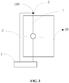
- FIG. 3 is a schematic diagram showing only the connection of the repair line 2 and the second signal line 3 in one repair line set 10 when repairing one of the first signal lines 1 in a display area 20 (the connecting line 4 between the second signal line 3 and the repair line 2 is not shown in FIG. 3 ).
- a break point which is indicated by a circle on the first signal line 1 in FIG. 3 , occurs in the first signal line 1
- the repair line 2 is electrically connected to the first signal line 1 at a first position 100 (where they intersect with each other)
- the second signal line 3 is electrically connected to the repair line 2 (where the second signal line 3 is not electrically connected to the repair line 2 in the normal operating state of the first signal line 1).
- the array substrate includes a base substrate BS, which is provided thereon with a plurality of first signal lines 1 and also with a plurality of repair line sets 10 configured to repair the plurality of first signal lines 1.
- Each of the repair line sets 10 includes:
- FIG. 2 is a schematic diagram showing only two repair line sets 10 sharing one second signal line 3, but the present disclosure is not limited thereto, and the number of the repair line sets sharing the one second signal line may be set based on actual needs.
- FIG. 3 is a schematic diagram showing only the connection of the repair line 2 and the second signal line 3 in one repair line set 10 when repairing one of the first signal lines 1 in a display area 20 (the connecting line between the second signal line and the repair line is not shown in FIG. 3 ).
- a break point which is indicated by a circle on the first signal line 1 in FIG.
- the repair line 2 is electrically connected to the first signal line 1 at a first position 100 (where they intersect with each other), and the second signal line 3 is electrically connected to the repair line 2 (where the second signal line 3 is not electrically connected to the repair line 2 in the normal operating state of the first signal line 1).
- the driving circuit 7 can transmit a signal to the first signal line 1 through the second signal line 3 and the repair line 2.
- the display of the entire display area 20 is not affected except for the region of the break point on the first signal line 1.
- the first signal line 1 is, for example, a data line or a gate line.
- a data line is connected to a corresponding source driving circuit, and the source driving circuit transmits a data signal to the data line connected thereto.
- the first signal line 1 is a data line and the data line fails (a defect such as a break occurs), the data line needs to be repaired.
- the source driving circuit can supply a data signal to the failed data line through the corresponding second signal line 3 and the repair line 2, and the normal display will not be affected.
- a gate line in a normal operating state, a gate line is connected to a corresponding gate driving circuit, and the gate driving circuit transmits a gate driving signal to the gate line connected thereto.
- the gate driving circuit transmits a gate driving signal to the gate line connected thereto.
- the gate driving circuit can supply a data signal to the failed gate line through the corresponding second signal line 3 and the repair line 2, and the normal display will not be affected.
- the two lines can be arranged in a same layer or different layers.
- a bridge type connection can be used, and the two lines are insulated from each other at the bridge type connection.
- the two lines may be arranged to cross orthogonally or at a certain angle, and they are substantially insulated from each other at their cross point.
- the spacer is arranged to intersect with and be insulated from the repair line, it should be understood by those skilled in the art that it means that an orthogonal projection of the repair line on the base substrate overlaps at least a portion of the spacer, or the entire spacer and they are substantially insulated from each other at their intersection.
- embodiments of the present disclosure provide a method for repairing an array substrate, which is applied to the array substrate as described above.
- the method includes: if the first signal line corresponding to one of the plurality of repair line sets is broken, causing the broken first signal line to be electrically connected to the repair line contained in the repair line set corresponding to the broken first signal line at a first position; and causing the repair line contained in the repair line set corresponding to the broken first signal line to be electrically connected to the second signal line at a second position.
- the first position is an intersection of the broken first signal line and the repair line contained in the repair line set corresponding to the broken first signal line
- the second position is an intersection of the second signal line and the repair line contained in the repair line set corresponding to the broken first signal line.
- embodiments of the present disclosure further provide a display device including the array substrate as described above.
- the display device may be any product or component having a display function, such as a liquid crystal television (TV), a liquid crystal display (LCD), a digital photo frame, a mobile phone, a tablet computer, etc.
- the display device further includes a flexible circuit board, a printed circuit board, and a backplane.
Landscapes
- Physics & Mathematics (AREA)
- Nonlinear Science (AREA)
- Mathematical Physics (AREA)
- Chemical & Material Sciences (AREA)
- Crystallography & Structural Chemistry (AREA)
- General Physics & Mathematics (AREA)
- Optics & Photonics (AREA)
- Engineering & Computer Science (AREA)
- Microelectronics & Electronic Packaging (AREA)
- Devices For Indicating Variable Information By Combining Individual Elements (AREA)
- Liquid Crystal (AREA)
- Manufacturing & Machinery (AREA)
Applications Claiming Priority (2)
| Application Number | Priority Date | Filing Date | Title |
|---|---|---|---|
| CN201821480470.2U CN208588882U (zh) | 2018-09-11 | 2018-09-11 | 阵列基板及显示装置 |
| PCT/CN2019/087181 WO2020052262A1 (fr) | 2018-09-11 | 2019-05-16 | Substrat matriciel et procédé pour le réparer, et dispositif d'affichage |
Publications (3)
| Publication Number | Publication Date |
|---|---|
| EP3851908A1 true EP3851908A1 (fr) | 2021-07-21 |
| EP3851908A4 EP3851908A4 (fr) | 2022-06-08 |
| EP3851908B1 EP3851908B1 (fr) | 2024-09-04 |
Family
ID=65545178
Family Applications (1)
| Application Number | Title | Priority Date | Filing Date |
|---|---|---|---|
| EP19812889.4A Active EP3851908B1 (fr) | 2018-09-11 | 2019-05-16 | Substrat matriciel et procédé pour le réparer, et dispositif d'affichage |
Country Status (4)
| Country | Link |
|---|---|
| US (1) | US11251204B2 (fr) |
| EP (1) | EP3851908B1 (fr) |
| CN (1) | CN208588882U (fr) |
| WO (1) | WO2020052262A1 (fr) |
Families Citing this family (1)
| Publication number | Priority date | Publication date | Assignee | Title |
|---|---|---|---|---|
| CN208588882U (zh) * | 2018-09-11 | 2019-03-08 | 京东方科技集团股份有限公司 | 阵列基板及显示装置 |
Family Cites Families (10)
| Publication number | Priority date | Publication date | Assignee | Title |
|---|---|---|---|---|
| US5298891A (en) * | 1991-04-18 | 1994-03-29 | Thomson, S.A. | Data line defect avoidance structure |
| US6014191A (en) * | 1996-07-16 | 2000-01-11 | Samsung Electronics Co., Ltd. | Liquid crystal display having repair lines that cross data lines twice and cross gate lines in the active area and related repairing methods |
| KR101347846B1 (ko) * | 2006-12-27 | 2014-01-07 | 삼성디스플레이 주식회사 | 박막 트랜지스터 기판, 이를 포함하는 액정표시장치 및이의 리페어 방법 |
| CN101644838A (zh) * | 2009-09-03 | 2010-02-10 | 上海广电光电子有限公司 | 液晶面板修复线结构 |
| FR2956753B1 (fr) * | 2010-02-19 | 2012-07-06 | Thales Sa | Afficheur a matrice active a structure integree de reparation de lignes ouvertes. |
| TWI481941B (zh) | 2012-09-03 | 2015-04-21 | Au Optronics Corp | 顯示面板及其修補方法 |
| KR20150017192A (ko) * | 2013-08-06 | 2015-02-16 | 삼성디스플레이 주식회사 | 유기 발광 표시 장치 및 그 제조 방법 |
| CN103745970B (zh) * | 2013-12-31 | 2017-02-01 | 合肥京东方光电科技有限公司 | 阵列基板及其制作方法、修复方法、显示装置 |
| CN206758435U (zh) * | 2017-06-09 | 2017-12-15 | 信利半导体有限公司 | 一种阵列基板及显示装置 |
| CN208588882U (zh) * | 2018-09-11 | 2019-03-08 | 京东方科技集团股份有限公司 | 阵列基板及显示装置 |
-
2018
- 2018-09-11 CN CN201821480470.2U patent/CN208588882U/zh active Active
-
2019
- 2019-05-16 WO PCT/CN2019/087181 patent/WO2020052262A1/fr not_active Ceased
- 2019-05-16 EP EP19812889.4A patent/EP3851908B1/fr active Active
- 2019-05-16 US US16/610,673 patent/US11251204B2/en active Active
Also Published As
| Publication number | Publication date |
|---|---|
| EP3851908B1 (fr) | 2024-09-04 |
| EP3851908A4 (fr) | 2022-06-08 |
| US20200303420A1 (en) | 2020-09-24 |
| US11251204B2 (en) | 2022-02-15 |
| WO2020052262A1 (fr) | 2020-03-19 |
| CN208588882U (zh) | 2019-03-08 |
Similar Documents
| Publication | Publication Date | Title |
|---|---|---|
| US9508751B2 (en) | Array substrate, method for manufacturing the same and display device | |
| US9397123B1 (en) | Array substrate, manufacture method thereof, and display device | |
| US9678400B2 (en) | Array substrate for liquid crystal display and manufacturing method thereof | |
| US7834360B2 (en) | Thin film transistor array substrate | |
| US9465256B2 (en) | Liquid crystal display panel and manufacturing method thereof | |
| US9627416B2 (en) | Array substrate and method for manufacturing the same, display device | |
| CN108803177A (zh) | 阵列基板、显示面板及其检测方法 | |
| US20230170356A1 (en) | Array substrate and display device | |
| WO2020119548A1 (fr) | Procédé de réparation d'écran d'affichage et écran d'affichage | |
| CN107123384B (zh) | 一种显示基板的测试方法及应用于显示设备的基板 | |
| US9335596B2 (en) | Array substrate, display device, and repair method for the array substrate | |
| JP6881981B2 (ja) | アレイ基板、表示装置及びアレイ基板の製造方法 | |
| US7990486B2 (en) | Liquid crystal display panel with line defect repairing mechanism and repairing method thereof | |
| US11251204B2 (en) | Array substrate, method for repairing same, and display device | |
| CN104484067A (zh) | 触控面板及其制作方法、显示面板及触控显示装置 | |
| CN108594548B (zh) | 液晶面板扇出区及液晶面板 | |
| JP7745099B2 (ja) | アレイ基板、表示パネル及び表示装置 | |
| US10396100B2 (en) | Array substrate, display panel and pixel patching method | |
| CN106601162B (zh) | 显示面板及包含其的显示装置 | |
| CN106647081B (zh) | 阵列基板、液晶显示面板和液晶显示装置 | |
| KR0151269B1 (ko) | 액정표시장치 | |
| CN113126348A (zh) | 液晶显示基板及液晶显示基板的制作方法 | |
| JP2622174B2 (ja) | マトリクス型表示装置 | |
| CN110764328A (zh) | 显示基板及其维修方法、和显示装置 | |
| KR20000053415A (ko) | 액정 디스플레이 디바이스, 액정 디스플레이 패널용 기판및 액정 디스플레이 패널의 제조 방법 |
Legal Events
| Date | Code | Title | Description |
|---|---|---|---|
| STAA | Information on the status of an ep patent application or granted ep patent |
Free format text: STATUS: UNKNOWN |
|
| STAA | Information on the status of an ep patent application or granted ep patent |
Free format text: STATUS: THE INTERNATIONAL PUBLICATION HAS BEEN MADE |
|
| PUAI | Public reference made under article 153(3) epc to a published international application that has entered the european phase |
Free format text: ORIGINAL CODE: 0009012 |
|
| STAA | Information on the status of an ep patent application or granted ep patent |
Free format text: STATUS: REQUEST FOR EXAMINATION WAS MADE |
|
| 17P | Request for examination filed |
Effective date: 20191210 |
|
| AK | Designated contracting states |
Kind code of ref document: A1 Designated state(s): AL AT BE BG CH CY CZ DE DK EE ES FI FR GB GR HR HU IE IS IT LI LT LU LV MC MK MT NL NO PL PT RO RS SE SI SK SM TR |
|
| DAV | Request for validation of the european patent (deleted) | ||
| DAX | Request for extension of the european patent (deleted) | ||
| A4 | Supplementary search report drawn up and despatched |
Effective date: 20220511 |
|
| RIC1 | Information provided on ipc code assigned before grant |
Ipc: G02F 1/1345 20060101ALI20220504BHEP Ipc: H01L 27/12 20060101ALI20220504BHEP Ipc: G02F 1/1362 20060101AFI20220504BHEP |
|
| STAA | Information on the status of an ep patent application or granted ep patent |
Free format text: STATUS: EXAMINATION IS IN PROGRESS |
|
| 17Q | First examination report despatched |
Effective date: 20230609 |
|
| GRAP | Despatch of communication of intention to grant a patent |
Free format text: ORIGINAL CODE: EPIDOSNIGR1 |
|
| STAA | Information on the status of an ep patent application or granted ep patent |
Free format text: STATUS: GRANT OF PATENT IS INTENDED |
|
| INTG | Intention to grant announced |
Effective date: 20240626 |
|
| GRAS | Grant fee paid |
Free format text: ORIGINAL CODE: EPIDOSNIGR3 |
|
| GRAA | (expected) grant |
Free format text: ORIGINAL CODE: 0009210 |
|
| STAA | Information on the status of an ep patent application or granted ep patent |
Free format text: STATUS: THE PATENT HAS BEEN GRANTED |
|
| AK | Designated contracting states |
Kind code of ref document: B1 Designated state(s): AL AT BE BG CH CY CZ DE DK EE ES FI FR GB GR HR HU IE IS IT LI LT LU LV MC MK MT NL NO PL PT RO RS SE SI SK SM TR |
|
| REG | Reference to a national code |
Ref country code: GB Ref legal event code: FG4D |
|
| REG | Reference to a national code |
Ref country code: CH Ref legal event code: EP |
|
| REG | Reference to a national code |
Ref country code: IE Ref legal event code: FG4D |
|
| REG | Reference to a national code |
Ref country code: DE Ref legal event code: R096 Ref document number: 602019058395 Country of ref document: DE |
|
| REG | Reference to a national code |
Ref country code: LT Ref legal event code: MG9D |
|
| REG | Reference to a national code |
Ref country code: NL Ref legal event code: MP Effective date: 20240904 |
|
| PG25 | Lapsed in a contracting state [announced via postgrant information from national office to epo] |
Ref country code: NO Free format text: LAPSE BECAUSE OF FAILURE TO SUBMIT A TRANSLATION OF THE DESCRIPTION OR TO PAY THE FEE WITHIN THE PRESCRIBED TIME-LIMIT Effective date: 20241204 |
|
| PG25 | Lapsed in a contracting state [announced via postgrant information from national office to epo] |
Ref country code: FI Free format text: LAPSE BECAUSE OF FAILURE TO SUBMIT A TRANSLATION OF THE DESCRIPTION OR TO PAY THE FEE WITHIN THE PRESCRIBED TIME-LIMIT Effective date: 20240904 Ref country code: GR Free format text: LAPSE BECAUSE OF FAILURE TO SUBMIT A TRANSLATION OF THE DESCRIPTION OR TO PAY THE FEE WITHIN THE PRESCRIBED TIME-LIMIT Effective date: 20241205 Ref country code: PL Free format text: LAPSE BECAUSE OF FAILURE TO SUBMIT A TRANSLATION OF THE DESCRIPTION OR TO PAY THE FEE WITHIN THE PRESCRIBED TIME-LIMIT Effective date: 20240904 |
|
| PG25 | Lapsed in a contracting state [announced via postgrant information from national office to epo] |
Ref country code: BG Free format text: LAPSE BECAUSE OF FAILURE TO SUBMIT A TRANSLATION OF THE DESCRIPTION OR TO PAY THE FEE WITHIN THE PRESCRIBED TIME-LIMIT Effective date: 20240904 |
|
| PG25 | Lapsed in a contracting state [announced via postgrant information from national office to epo] |
Ref country code: LV Free format text: LAPSE BECAUSE OF FAILURE TO SUBMIT A TRANSLATION OF THE DESCRIPTION OR TO PAY THE FEE WITHIN THE PRESCRIBED TIME-LIMIT Effective date: 20240904 |
|
| PG25 | Lapsed in a contracting state [announced via postgrant information from national office to epo] |
Ref country code: HR Free format text: LAPSE BECAUSE OF FAILURE TO SUBMIT A TRANSLATION OF THE DESCRIPTION OR TO PAY THE FEE WITHIN THE PRESCRIBED TIME-LIMIT Effective date: 20240904 |
|
| PG25 | Lapsed in a contracting state [announced via postgrant information from national office to epo] |
Ref country code: ES Free format text: LAPSE BECAUSE OF FAILURE TO SUBMIT A TRANSLATION OF THE DESCRIPTION OR TO PAY THE FEE WITHIN THE PRESCRIBED TIME-LIMIT Effective date: 20240904 Ref country code: RS Free format text: LAPSE BECAUSE OF FAILURE TO SUBMIT A TRANSLATION OF THE DESCRIPTION OR TO PAY THE FEE WITHIN THE PRESCRIBED TIME-LIMIT Effective date: 20241204 |
|
| PG25 | Lapsed in a contracting state [announced via postgrant information from national office to epo] |
Ref country code: RS Free format text: LAPSE BECAUSE OF FAILURE TO SUBMIT A TRANSLATION OF THE DESCRIPTION OR TO PAY THE FEE WITHIN THE PRESCRIBED TIME-LIMIT Effective date: 20241204 Ref country code: PL Free format text: LAPSE BECAUSE OF FAILURE TO SUBMIT A TRANSLATION OF THE DESCRIPTION OR TO PAY THE FEE WITHIN THE PRESCRIBED TIME-LIMIT Effective date: 20240904 Ref country code: NO Free format text: LAPSE BECAUSE OF FAILURE TO SUBMIT A TRANSLATION OF THE DESCRIPTION OR TO PAY THE FEE WITHIN THE PRESCRIBED TIME-LIMIT Effective date: 20241204 Ref country code: LV Free format text: LAPSE BECAUSE OF FAILURE TO SUBMIT A TRANSLATION OF THE DESCRIPTION OR TO PAY THE FEE WITHIN THE PRESCRIBED TIME-LIMIT Effective date: 20240904 Ref country code: HR Free format text: LAPSE BECAUSE OF FAILURE TO SUBMIT A TRANSLATION OF THE DESCRIPTION OR TO PAY THE FEE WITHIN THE PRESCRIBED TIME-LIMIT Effective date: 20240904 Ref country code: GR Free format text: LAPSE BECAUSE OF FAILURE TO SUBMIT A TRANSLATION OF THE DESCRIPTION OR TO PAY THE FEE WITHIN THE PRESCRIBED TIME-LIMIT Effective date: 20241205 Ref country code: FI Free format text: LAPSE BECAUSE OF FAILURE TO SUBMIT A TRANSLATION OF THE DESCRIPTION OR TO PAY THE FEE WITHIN THE PRESCRIBED TIME-LIMIT Effective date: 20240904 Ref country code: ES Free format text: LAPSE BECAUSE OF FAILURE TO SUBMIT A TRANSLATION OF THE DESCRIPTION OR TO PAY THE FEE WITHIN THE PRESCRIBED TIME-LIMIT Effective date: 20240904 Ref country code: BG Free format text: LAPSE BECAUSE OF FAILURE TO SUBMIT A TRANSLATION OF THE DESCRIPTION OR TO PAY THE FEE WITHIN THE PRESCRIBED TIME-LIMIT Effective date: 20240904 |
|
| REG | Reference to a national code |
Ref country code: AT Ref legal event code: MK05 Ref document number: 1720994 Country of ref document: AT Kind code of ref document: T Effective date: 20240904 |
|
| PG25 | Lapsed in a contracting state [announced via postgrant information from national office to epo] |
Ref country code: NL Free format text: LAPSE BECAUSE OF FAILURE TO SUBMIT A TRANSLATION OF THE DESCRIPTION OR TO PAY THE FEE WITHIN THE PRESCRIBED TIME-LIMIT Effective date: 20240904 |
|
| PG25 | Lapsed in a contracting state [announced via postgrant information from national office to epo] |
Ref country code: PT Free format text: LAPSE BECAUSE OF FAILURE TO SUBMIT A TRANSLATION OF THE DESCRIPTION OR TO PAY THE FEE WITHIN THE PRESCRIBED TIME-LIMIT Effective date: 20250106 Ref country code: IS Free format text: LAPSE BECAUSE OF FAILURE TO SUBMIT A TRANSLATION OF THE DESCRIPTION OR TO PAY THE FEE WITHIN THE PRESCRIBED TIME-LIMIT Effective date: 20250104 |
|
| PG25 | Lapsed in a contracting state [announced via postgrant information from national office to epo] |
Ref country code: RO Free format text: LAPSE BECAUSE OF FAILURE TO SUBMIT A TRANSLATION OF THE DESCRIPTION OR TO PAY THE FEE WITHIN THE PRESCRIBED TIME-LIMIT Effective date: 20240904 Ref country code: SM Free format text: LAPSE BECAUSE OF FAILURE TO SUBMIT A TRANSLATION OF THE DESCRIPTION OR TO PAY THE FEE WITHIN THE PRESCRIBED TIME-LIMIT Effective date: 20240904 |
|
| PG25 | Lapsed in a contracting state [announced via postgrant information from national office to epo] |
Ref country code: EE Free format text: LAPSE BECAUSE OF FAILURE TO SUBMIT A TRANSLATION OF THE DESCRIPTION OR TO PAY THE FEE WITHIN THE PRESCRIBED TIME-LIMIT Effective date: 20240904 Ref country code: AT Free format text: LAPSE BECAUSE OF FAILURE TO SUBMIT A TRANSLATION OF THE DESCRIPTION OR TO PAY THE FEE WITHIN THE PRESCRIBED TIME-LIMIT Effective date: 20240904 |
|
| PG25 | Lapsed in a contracting state [announced via postgrant information from national office to epo] |
Ref country code: CZ Free format text: LAPSE BECAUSE OF FAILURE TO SUBMIT A TRANSLATION OF THE DESCRIPTION OR TO PAY THE FEE WITHIN THE PRESCRIBED TIME-LIMIT Effective date: 20240904 |
|
| PG25 | Lapsed in a contracting state [announced via postgrant information from national office to epo] |
Ref country code: SK Free format text: LAPSE BECAUSE OF FAILURE TO SUBMIT A TRANSLATION OF THE DESCRIPTION OR TO PAY THE FEE WITHIN THE PRESCRIBED TIME-LIMIT Effective date: 20240904 Ref country code: IT Free format text: LAPSE BECAUSE OF FAILURE TO SUBMIT A TRANSLATION OF THE DESCRIPTION OR TO PAY THE FEE WITHIN THE PRESCRIBED TIME-LIMIT Effective date: 20240904 |
|
| REG | Reference to a national code |
Ref country code: DE Ref legal event code: R097 Ref document number: 602019058395 Country of ref document: DE |
|
| PGFP | Annual fee paid to national office [announced via postgrant information from national office to epo] |
Ref country code: DE Payment date: 20250519 Year of fee payment: 7 |
|
| PG25 | Lapsed in a contracting state [announced via postgrant information from national office to epo] |
Ref country code: DK Free format text: LAPSE BECAUSE OF FAILURE TO SUBMIT A TRANSLATION OF THE DESCRIPTION OR TO PAY THE FEE WITHIN THE PRESCRIBED TIME-LIMIT Effective date: 20240904 |
|
| PLBE | No opposition filed within time limit |
Free format text: ORIGINAL CODE: 0009261 |
|
| STAA | Information on the status of an ep patent application or granted ep patent |
Free format text: STATUS: NO OPPOSITION FILED WITHIN TIME LIMIT |
|
| 26N | No opposition filed |
Effective date: 20250605 |
|
| PG25 | Lapsed in a contracting state [announced via postgrant information from national office to epo] |
Ref country code: SE Free format text: LAPSE BECAUSE OF FAILURE TO SUBMIT A TRANSLATION OF THE DESCRIPTION OR TO PAY THE FEE WITHIN THE PRESCRIBED TIME-LIMIT Effective date: 20240904 |
|
| REG | Reference to a national code |
Ref country code: CH Ref legal event code: H13 Free format text: ST27 STATUS EVENT CODE: U-0-0-H10-H13 (AS PROVIDED BY THE NATIONAL OFFICE) Effective date: 20251223 |
|
| PG25 | Lapsed in a contracting state [announced via postgrant information from national office to epo] |
Ref country code: LU Free format text: LAPSE BECAUSE OF NON-PAYMENT OF DUE FEES Effective date: 20250516 |
|
| PG25 | Lapsed in a contracting state [announced via postgrant information from national office to epo] |
Ref country code: CH Free format text: LAPSE BECAUSE OF NON-PAYMENT OF DUE FEES Effective date: 20250531 |
|
| REG | Reference to a national code |
Ref country code: BE Ref legal event code: MM Effective date: 20250531 |
|
| PG25 | Lapsed in a contracting state [announced via postgrant information from national office to epo] |
Ref country code: MC Free format text: LAPSE BECAUSE OF FAILURE TO SUBMIT A TRANSLATION OF THE DESCRIPTION OR TO PAY THE FEE WITHIN THE PRESCRIBED TIME-LIMIT Effective date: 20240904 |
|
| PGFP | Annual fee paid to national office [announced via postgrant information from national office to epo] |
Ref country code: GB Payment date: 20260323 Year of fee payment: 8 |
|
| PG25 | Lapsed in a contracting state [announced via postgrant information from national office to epo] |
Ref country code: IE Free format text: LAPSE BECAUSE OF NON-PAYMENT OF DUE FEES Effective date: 20250516 |
|
| PG25 | Lapsed in a contracting state [announced via postgrant information from national office to epo] |
Ref country code: BE Free format text: LAPSE BECAUSE OF NON-PAYMENT OF DUE FEES Effective date: 20250531 |
|
| PG25 | Lapsed in a contracting state [announced via postgrant information from national office to epo] |
Ref country code: FR Free format text: LAPSE BECAUSE OF NON-PAYMENT OF DUE FEES Effective date: 20250531 |