EP3846221A1 - Halbleitervorrichtung und verfahren zu ihrer herstellung sowie eine schnelle diode und verfahren zu ihrer herstellung - Google Patents
Halbleitervorrichtung und verfahren zu ihrer herstellung sowie eine schnelle diode und verfahren zu ihrer herstellung Download PDFInfo
- Publication number
- EP3846221A1 EP3846221A1 EP19854678.0A EP19854678A EP3846221A1 EP 3846221 A1 EP3846221 A1 EP 3846221A1 EP 19854678 A EP19854678 A EP 19854678A EP 3846221 A1 EP3846221 A1 EP 3846221A1
- Authority
- EP
- European Patent Office
- Prior art keywords
- substrate
- layer
- conductivity type
- semiconductor layer
- insulating protrusions
- Prior art date
- Legal status (The legal status is an assumption and is not a legal conclusion. Google has not performed a legal analysis and makes no representation as to the accuracy of the status listed.)
- Pending
Links
Images







Classifications
-
- H—ELECTRICITY
- H10—SEMICONDUCTOR DEVICES; ELECTRIC SOLID-STATE DEVICES NOT OTHERWISE PROVIDED FOR
- H10D—INORGANIC ELECTRIC SEMICONDUCTOR DEVICES
- H10D8/00—Diodes
-
- H—ELECTRICITY
- H10—SEMICONDUCTOR DEVICES; ELECTRIC SOLID-STATE DEVICES NOT OTHERWISE PROVIDED FOR
- H10D—INORGANIC ELECTRIC SEMICONDUCTOR DEVICES
- H10D12/00—Bipolar devices controlled by the field effect, e.g. insulated-gate bipolar transistors [IGBT]
- H10D12/01—Manufacture or treatment
- H10D12/031—Manufacture or treatment of IGBTs
- H10D12/032—Manufacture or treatment of IGBTs of vertical IGBTs
-
- H—ELECTRICITY
- H10—SEMICONDUCTOR DEVICES; ELECTRIC SOLID-STATE DEVICES NOT OTHERWISE PROVIDED FOR
- H10D—INORGANIC ELECTRIC SEMICONDUCTOR DEVICES
- H10D12/00—Bipolar devices controlled by the field effect, e.g. insulated-gate bipolar transistors [IGBT]
- H10D12/411—Insulated-gate bipolar transistors [IGBT]
- H10D12/441—Vertical IGBTs
-
- H—ELECTRICITY
- H10—SEMICONDUCTOR DEVICES; ELECTRIC SOLID-STATE DEVICES NOT OTHERWISE PROVIDED FOR
- H10D—INORGANIC ELECTRIC SEMICONDUCTOR DEVICES
- H10D62/00—Semiconductor bodies, or regions thereof, of devices having potential barriers
- H10D62/10—Shapes, relative sizes or dispositions of the regions of the semiconductor bodies; Shapes of the semiconductor bodies
- H10D62/113—Isolations within a component, i.e. internal isolations
- H10D62/115—Dielectric isolations, e.g. air gaps
-
- H—ELECTRICITY
- H10—SEMICONDUCTOR DEVICES; ELECTRIC SOLID-STATE DEVICES NOT OTHERWISE PROVIDED FOR
- H10D—INORGANIC ELECTRIC SEMICONDUCTOR DEVICES
- H10D64/00—Electrodes of devices having potential barriers
- H10D64/20—Electrodes characterised by their shapes, relative sizes or dispositions
- H10D64/23—Electrodes carrying the current to be rectified, amplified, oscillated or switched, e.g. sources, drains, anodes or cathodes
- H10D64/232—Emitter electrodes for IGBTs
-
- H—ELECTRICITY
- H10—SEMICONDUCTOR DEVICES; ELECTRIC SOLID-STATE DEVICES NOT OTHERWISE PROVIDED FOR
- H10D—INORGANIC ELECTRIC SEMICONDUCTOR DEVICES
- H10D8/00—Diodes
- H10D8/01—Manufacture or treatment
- H10D8/045—Manufacture or treatment of PN junction diodes
-
- H—ELECTRICITY
- H10—SEMICONDUCTOR DEVICES; ELECTRIC SOLID-STATE DEVICES NOT OTHERWISE PROVIDED FOR
- H10W—GENERIC PACKAGES, INTERCONNECTIONS, CONNECTORS OR OTHER CONSTRUCTIONAL DETAILS OF DEVICES COVERED BY CLASS H10
- H10W72/00—Interconnections or connectors in packages
-
- H—ELECTRICITY
- H10—SEMICONDUCTOR DEVICES; ELECTRIC SOLID-STATE DEVICES NOT OTHERWISE PROVIDED FOR
- H10D—INORGANIC ELECTRIC SEMICONDUCTOR DEVICES
- H10D62/00—Semiconductor bodies, or regions thereof, of devices having potential barriers
- H10D62/80—Semiconductor bodies, or regions thereof, of devices having potential barriers characterised by the materials
- H10D62/83—Semiconductor bodies, or regions thereof, of devices having potential barriers characterised by the materials being Group IV materials, e.g. B-doped Si or undoped Ge
- H10D62/834—Semiconductor bodies, or regions thereof, of devices having potential barriers characterised by the materials being Group IV materials, e.g. B-doped Si or undoped Ge further characterised by the dopants
-
- H—ELECTRICITY
- H10—SEMICONDUCTOR DEVICES; ELECTRIC SOLID-STATE DEVICES NOT OTHERWISE PROVIDED FOR
- H10W—GENERIC PACKAGES, INTERCONNECTIONS, CONNECTORS OR OTHER CONSTRUCTIONAL DETAILS OF DEVICES COVERED BY CLASS H10
- H10W72/00—Interconnections or connectors in packages
- H10W72/90—Bond pads, in general
- H10W72/931—Shapes of bond pads
- H10W72/934—Cross-sectional shape, i.e. in side view
-
- H—ELECTRICITY
- H10—SEMICONDUCTOR DEVICES; ELECTRIC SOLID-STATE DEVICES NOT OTHERWISE PROVIDED FOR
- H10W—GENERIC PACKAGES, INTERCONNECTIONS, CONNECTORS OR OTHER CONSTRUCTIONAL DETAILS OF DEVICES COVERED BY CLASS H10
- H10W72/00—Interconnections or connectors in packages
- H10W72/90—Bond pads, in general
- H10W72/941—Dispositions of bond pads
- H10W72/944—Dispositions of multiple bond pads
Definitions
- the present application relates to the technical field of semiconductors, for example, a semiconductor device, a preparation method of a semiconductor device, a fast recovery diode, and a preparation method of a fast recovery diode.
- a semiconductor device is an electronic device that uses special electrical characteristics of semiconductor materials to complete specific functions, and the semiconductor device can be used to generate, control, receive, convert, amplify signals and convert energy.
- the semiconductor device has a wide range of applications, and is almost all applicable from electronics manufacturing (including computers, digital products, white goods, and the like) of the consumer field to the industrial control field (power equipment, rail transit, electric vehicles, photovoltaic, and the like).
- a metal layer is disposed on and parallel to one surface of a device body, and a vertical press force entirely acts on the device body via the metal layer.
- a conduction voltage of the semiconductor device gradually decreases, causing the imbalance between a voltage with standed by the device and an actual conduction current, thus causing concentrating distribution of heat, and thus causing stress damages to the semiconductor device by the vertical press force.
- a power fast recovery diode is a kind of two-terminal device with unilateral conduction.
- the semiconductor fast recovery diode is used in almost all electronic circuits, and plays an important role in many circuit power apparatuses.
- the fast recovery diode (FRD) is widely used in various fields due to good switching characteristics and relatively short reverse recovery time.
- the N - region namely, the low doping drift region
- the active region bears most of the electric field
- a large number of electron-hole pairs are separated under the action of the electric field
- electrons move to the N + high potential so as to form an electron current
- holes move to the P + low potential so as to form a hole current
- a sum of the electron current and the hole current is a reverse leakage current.
- the N - drift region has a carrier lifetime control layer, defects forming the lifetime control layer will generate more electrons and holes under the action of a reverse electric field, and the reverse leakage current will further increase, resulting in increased losses in the state of reverse cutoff.
- Embodiments of the present application provide a semiconductor device and a preparation method of a semiconductor device so as to solve the problem of stress damage caused by the structure of the semiconductor device in the related art.
- Embodiments of the present application provide a fast recovery diode and a preparation method of a fast recovery diode so as to solve the problem that the fast recovery diode in the related art has a large leakage current in a state of reverse cutoff.
- a semiconductor device including a substrate with a first conductivity type, a first semiconductor layer with a second conductivity type, a plurality of discrete first insulating protrusions, and a first metal electrode layer.
- the first semiconductor layer is formed on a first surface of the substrate, and the second conductivity type is opposite to the first conductivity type.
- the plurality of discrete first insulating protrusions are formed on the first semiconductor layer.
- the first metal electrode layer is formed on the plurality of discrete first insulating protrusions.
- a first semiconductor layer with a second conductivity type is formed on a first surface of a substrate with a first conductivity type, where the first conductivity type is opposite to the second conductivity type.
- a plurality of discrete first insulating protrusions are formed on the first semiconductor layer.
- a first metal electrode layer is formed on the plurality of discrete first insulating protrusions.
- a fast recovery diode including a substrate with a first conductivity type, a semiconductor layer with a second conductivity type, and a doped layer.
- the semiconductor layer with the second conductivity type is formed on the substrate, where the second conductivity type is opposite to the first conductivity type.
- the doped layer is formed in the substrate and has a same conductivity type as the substrate.
- the doped layer is obtained by injecting doped ions into the substrate and being annealed at a predetermined temperature, and the predetermined temperature is less than 500°C.
- a substrate with a first conductivity type is provided.
- a semiconductor layer with a second conductivity type is formed on the substrate, and the second conductivity type is opposite to the first conductivity type.
- Doped ions are injected into the substrate.
- the substrate with the doped ions injected is annealed at a predetermined temperature so as to form a doped layer having a same conductivity type as the substrate, where the predetermined temperature is less than 500°C.
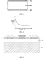
- Packaging modes of a semiconductor device include welding and press. Under the conditions of long-term operation or environmental aging, welding packaging is easy to cause excessive concentration of thermal stress at the welding part, resulting in easy degradation and failure of power semiconductor devices; while press packaging uses a mode in which electrical power terminals is elastically crimped with the semiconductor device to achieve durable electrical contact, thus avoiding thermal stress accumulation.
- a semiconductor device includes a device body 10 (the device body 10 includes a substrate and a semiconductor layer having a conductive type opposite to a conductive type of the substrate), and metal layers 20 disposed on two sides of the device body 10, respectively, where the metal layers 20 serve as electrodes of the power semiconductor device.
- a vertical press force is applied to the electrodes of the semiconductor device, so as to achieve electrical contact between the semiconductor device and an electrical power terminal.
- the vertical press force entirely acts on the device body via the metal layer.
- a conduction voltage of the semiconductor device gradually decreases, causing the imbalance between a voltage with standed by the device and an actual conduction current, thus causing concentrating distribution of heat, and thus causing stress damages to the semiconductor device by the vertical press force.
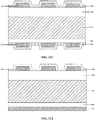
- Embodiments of the present application provide a semiconductor device, as shown in FIG. 3 , the semiconductor device includes a substrate 110, a first semiconductor layer 120 formed on a first surface of the substrate 110, a plurality of first insulating protrusions 141 formed on the first semiconductor layer 120, and a first metal electrode layer 150 formed on the plurality of first insulating protrusions 141.
- the substrate 110 has a first conductivity type
- the first semiconductor layer 120 has a second conductivity type
- the first conductivity type is opposite to the second conductivity type.
- the first conductivity type is an N-type
- the second conductivity type is a P-type
- the first conductivity type is a P-type
- the second conductivity type is an N-type.
- the case where the first conductivity type is an N-type and the second conductivity type is a P-type is described as an example, that is, the substrate 110 is the N-type substrate and the first semiconductor layer 120 is the P-type semiconductor layer.
- the first metal electrode layer 150 is formed on the plurality of first insulating protrusions 141, and is connected to the first semiconductor layer 120 via gaps between every two adjacent first insulating protrusions 141.
- the first insulating protrusions 141 are formed in an active region of the semiconductor device.
- the plurality of discrete first insulating protrusions 141 are provided such that the first metal electrode layer 150 has a concave-convex structure with respect to the substrate 110.
- the first metal electrode layer 150 is transversely deformed due to the existence of the first insulating protrusions 141, such that part of the vertical press force is dispersed through the transverse deformation of the first metal electrode layer 150.
- the press force acting on the first semiconductor layer 120 and the substrate 110 is reduced, and the stress damage to the semiconductor device caused by vertical press force is relieved, thereby preventing the semiconductor device from being burned down due to pressure or thermal stress, and improving the working stability of the semiconductor device.
- heights of the first insulating protrusions 141 each are within a range of 1000 ⁇ to 50 ⁇ m, and the distance between every two adjacent first insulating protrusions 141 is within a range of 1 ⁇ m to 100 ⁇ m.
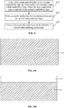
- the heights of the first insulating protrusions 141 and the distance between every two adjacent first insulating protrusions 141 are set. In this way, compared with the semiconductor device shown in FIG. 1 , the semiconductor device provided by this embodiment can ensure that the maximum attenuation ratio of the forward voltage drop with the pressure can be reduced by 3% (the maximum attenuation ratio of the forward voltage drop with the pressure of the semiconductor device shown in FIG. 1 is 15%).
- a thickness of the first metal electrode layer 150 is within a range of 1 ⁇ m to 100 ⁇ m.
- the vertical press force acting on the device is relieved through the thickness of the first metal electrode layer 150, that is, part of the vertical press force is dispersed by the transverse deformation of the first metal electrode layer 150, so as to reduce the vertical press force acting on the device and avoid the stress damage.
- the first metal electrode layer includes at least one metal layer, where the first metal electrode layer is made of at least one of aluminum, titanium, nickel, silver, and copper. That is to say, a number of metal layers provided in the first metal electrode layer may be specifically set according to the actual situation. The thicker the first metal electrode layer is, the more apparent the effect of pressure relief is. One metal layer, two metal layers, three metal layers or the like may be provided in the first metal electrode layer, and the thicknesses of the metal layers may be the same or different, or the materials of the metal layers may be the same or different.
- a number of the first insulating protrusions 141 may be specifically set according to the actual situation, so long as that the first metal electrode layer 150 formed on the first insulating protrusions 141 has a concave-convex structure with respect to the substrate 110 can be ensured.
- the first insulating protrusions 141 are made of silicon dioxide, boron-phosphorosilicate glass, phosphorosilicate glass, undoped silica glass, silicon nitride or silicon oxynitride.
- the first insulating protrusions 141 are formed between the first metal electrode layer 150 and the first semiconductor layer 120 such that the first insulating protrusions 141 further functions as a passivation layer, that is, the first insulating protrusions 141 can be used to prevent metal ions in the first metal electrode layer 150 from diffusing downward, thereby protecting the interior of the substrate 110 and the interface at the substrate 110 from contamination, and improving the working stability of the semiconductor device.
- FIG. 4 shows projections of the first insulating protrusions 141 on the first semiconductor layer 120.
- the shapes of projections of the first insulating protrusions 141 on the first semiconductor layer 120 are one or more of a polygon (such as a hexagon or a square), a strip, a ring, or a circle.
- the semiconductor device in this embodiment further includes a second semiconductor layer 130 formed on a second surface of the substrate, and a conductivity type of the second semiconductor layer 130 is the same as a conductivity type of the substrate 110.
- a second metal electrode layer 160 is formed on one surface of the second semiconductor layer 130, and the second metal electrode layer 160 cooperates with the first metal electrode layer 150 formed on the surfaces of the first insulating protrusions 141 to form electrodes of the semiconductor device.
- the substrate 110 is an N-type
- the first semiconductor layer 120 formed on the first surface of the substrate 110 is a P-type
- the second semiconductor layer 130 formed on the second surface of the substrate 110 is an N-type.
- the semiconductor device in this embodiment is an insulated gate bipolar transistor, a fast recovery diode or a gate control transistor.
- the substrate 110 serves as a voltage-withstand layer (N-type) of the fast recovery diode
- the first semiconductor layer 120 serves as a P-type buffer layer of the fast recovery diode
- the second semiconductor layer 130 serves as an N-type buffer layer of the fast recovery diode
- the first metal electrode layer 150 and the second metal electrode layer 160 serve as a positive electrode and a negative electrode of the fast recovery diode, respectively.
- Embodiments of the present application further provides a semiconductor device, as shown in FIG. 6 , the semiconductor device includes a substrate 210, a first semiconductor layer 220 formed on the substrate 210, a plurality of first insulating protrusions 241 formed on the first semiconductor layer 220, a first metal electrode layer 250 formed on the plurality of first insulating protrusions 241, a second semiconductor layer 230 formed on the substrate 210, a plurality of second insulating protrusions 242 formed on the second semiconductor layer 230, and a second metal electrode layer 260 formed on the plurality of second insulating protrusions 242.
- the plurality of discrete second insulating protrusions 242 are formed between the second semiconductor layer 230 and the second metal electrode layer 260.
- the second insulating protrusions 242 are used for relieving and reducing the vertical press force acting on the first semiconductor layer 220 and the substrate 210, relieving stress damage to the device caused by vertical press force, thereby preventing the device from being burned down due to pressure or thermal stress, and improving the working stability of the device.
- Specific structural details of the second insulating protrusions 242 may refer to related descriptions of the first insulating protrusions 141 in the embodiments shown in FIG. 3 to FIG. 5 , and the specific structural details will not be repeated herein.
- the heights of the second insulating protrusions 242, the distance between every two adjacent second insulating protrusions 242, the materials of the second insulating protrusions 242, the number of second insulating protrusions 242, or the projection shapes of the second insulating protrusions 242 on the substrate may be the same as or different from the heights of the first insulating protrusions 141, the distance between every two adjacent first insulating protrusions 141, the materials of the first insulating protrusions 141, the number of first insulating protrusions 141, and the projection shapes of the first insulating protrusions 141 on the substrate, respectively, and may be specifically set according to the actual requirements of the semiconductor device.
- Embodiments of the present application further provides a semiconductor device, as shown in FIG. 7 , the semiconductor device includes a voltage-withstand layer 301 (N-type), an N-type buffer layer 302, a P-type injected region 303, an N-type injected region 304, a rear P-type injected region 305, an injected oxidation layer 306, polycrystalline silicon 307, an oxidation layer 308, a dielectric layer 309, a front electrode 310, and a rear electrode 311.
- N-type voltage-withstand layer 301
- N-type buffer layer 302 the semiconductor device includes a voltage-withstand layer 301 (N-type), an N-type buffer layer 302, a P-type injected region 303, an N-type injected region 304, a rear P-type injected region 305, an injected oxidation layer 306, polycrystalline silicon 307, an oxidation layer 308, a dielectric layer 309, a front electrode 310, and a rear electrode 311.
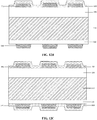
- Embodiments of the present application further provide a preparation method of a semiconductor device. As shown in FIG. 8 , the method includes steps described below.
- a first semiconductor layer with a second conductivity type is formed on a first surface of a substrate with a first conductivity type, where the first conductivity type is opposite to the second conductivity type.
- a substrate 110 with the first conductivity type is provided.
- the first semiconductor layer 120 with the second conductivity type is formed on the substrate 110.
- the first conductivity type is opposite to the second conductivity type.
- the case where the first conductivity type is the N-type and the second conductivity type is the P-type is described as an example in detail, that is, the substrate 110 is the N-type substrate, and the first semiconductor layer 120 is the P-type semiconductor layer.
- a P-type doping injectation window is formed after gluing and development, P-type impurities such as boron are injected, the glue is removed, a junction is pushed after cleaning, and a P-type buffer layer (that is, the first semiconductor layer 120) with a certain junction depth is formed.
- the plurality of discrete first insulating protrusions 141 are formed on the first semiconductor layer 120.
- the first insulating protrusions 141 may all be formed by etching the dielectric layer, or the first insulating protrusions 141 may be separately prepared.
- a first metal electrode layer is formed on the plurality of discrete first insulating protrusions.
- the first metal electrode layer 141 is formed on the first insulating protrusions 141.
- the metal layer may be grown by evaporation or sputtering so as to form the first metal electrode layer 141.
- the plurality of discrete first insulating protrusions 141 are formed on the first semiconductor layer 120 such that the first metal electrode layer 150 has a concave-convex structure with respect to the substrate 110.
- the first metal electrode layer 150 is transversely deformed due to the existence of the first insulating protrusions, such that part of the vertical press force is dispersed through the transverse deformation of the first metal electrode layer 150.
- the vertical press force acting on the first semiconductor layer and the substrate 110 is reduced, and the stress damage to the semiconductor device caused by vertical press force is relieved, thereby preventing the semiconductor device from being burned down due to pressure or thermal stress, and improving the working stability of the semiconductor device.
- S20 includes steps described below.
- a dielectric layer is formed on the first semiconductor layer.
- the dielectric layer 140 is formed on the first semiconductor layer.
- the dielectric layer 140 may be formed by thermal growth, chemical vapor deposition, physical vapor deposition, or the like.
- a thickness of the formed dielectric layer 140 is within a range of 1000 ⁇ to 50 ⁇ m.
- the dielectric layer is patterned, a part of the dielectric layer is removed such that one surface of the first semiconductor layer is exposed so as to form the plurality of discrete first insulating protrusions.
- an etching window is formed after gluing and development, the dielectric layer 140 is etched in a wet mode or in a dry mode, so that the plurality of discrete first insulating protrusions 141 are formed on the active region.
- the preparation method in this embodiment further includes forming a second semiconductor layer 130 on a second surface of the substrate 110, and the specific structure is shown in FIG. 5 .
- N-type impurities such as phosphorus or arsenic are injected into the second surface of the substrate 110, and the second semiconductor layer 130 is formed after the junction is pushed. That is to say, before S20, the first semiconductor layer 120 and the second semiconductor layer 130 are formed on the substrate 110, respectively; or after S30, the second semiconductor layer 130 is formed on the second surface of the substrate 110.
- the method further includes forming a second metal electrode layer 160 on the second semiconductor layer 130, and the specific structure is shown in FIG. 5 .
- the second semiconductor layer 130 may be thinned or etched, and then be metalized to form the second metal electrode layer 160.
- a passivation layer may further be deposited on one surface of the first metal electrode layer 150 so as to prevent the one surface of the first metal electrode layer 150 from being corroded.
- the passivation layer may be made of polyimide or the like.
- Embodiments of the present application further provide a preparation method of a semiconductor device.
- dielectric layers 240 are formed on the first semiconductor layer 220 and the second semiconductor layer 230, respectively; then as shown in FIG. 11B , the two dielectric layers 240 are patterned to form the first insulating protrusions 241 and the second insulating protrusions 242, respectively; and finally, as shown in FIG. 11C , the first metal electrode layer 250 and the second metal electrode layer 260 are formed.
- the dielectric layer 240 is formed on the second semiconductor layer 230. As shown in FIG. 12B , the dielectric layer 240 is patterned so as to form the plurality of discrete second insulating protrusions 242. As shown in FIG. 12C , the second metal electrode layer 260 is formed on the plurality of discrete second insulating protrusions 242.
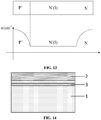
- FIG. 13 shows a structure of a fast recovery diode.
- the fast recovery diode includes a P-type semiconductor, an N-type semiconductor, and an intrinsic semiconductor i region added between the P-type silicon material and the N-type silicon material, thus constituting a P-i-N silicon wafer.
- a preparation method of the intrinsic semiconductor i region is to form a low concentration N - region between the P-type layer and the N-type layer, such that the N - region can be approximately considered as the intrinsic semiconductor i region compared with the P-type region and the N-type region.
- the working state of the fast recovery diode is generally divided into forward conduction and reverse cutoff.
- a local lifetime control region is formed inside the diode, and recombination centers with appropriate spatial distribution are introduced into the diode so as to control the lifetime of minority carriers, to further achieve the purposes of optimizing carrier distribution and diode performance parameters.
- the local lifetime control region is formed by utilizing the heavy metal diffusion process in conjunction with a relatively high annealing temperature (above 500°C).
- the N - region namely, the low doping drift region
- the active region bears most of the electric field
- a large number of electron-hole pairs are separated under the action of the electric field
- electrons move to the N + high potential so as to form an electron current
- holes move to the P + low potential so as to form a hole current
- a sum of the electron current and the hole current is a reverse leakage current.
- the N - drift region has a carrier lifetime control layer, defects forming the lifetime control layer will generate more electrons and holes under the action of a reverse electric field, and the reverse leakage current will further increase, resulting in increased losses in the state of reverse cutoff.
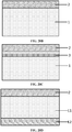
- the fast recovery diode includes a substrate 1 with a first conductivity type, a semiconductor layer 2 with a second conductivity type formed on the substrate 1, and at least one doped layer 3 formed in the substrate 1.
- the first conductivity type is opposite to the second conductivity type.
- the first conductivity type is the P-type
- the second conductivity type is the N-type
- the first conductivity type is the N-type
- the second conductivity type is the P-type.
- the case where the first conductivity type is the N-type and the second conductivity type is the P-type is described as an example in detail. That is to say, in this embodiment, the substrate 1 is the N-type substrate, and the semiconductor layer 2 is the P-type.
- the doped layer 3 has the same conductivity type as the substrate 1, and the doped layer 3 is obtained by injecting doped ions into the substrate 1 and being annealed at a predetermined temperature.
- the predetermined temperature is lower than 500°C.
- the annealing temperature is lower than 500°C such that the functional layer formed by injecting doped ions has the functions of both lifetime blocking and lifetime control, and the functional layer is the doped layer 3.
- the doped ions may include hydrogen ions, helium ions, phosphorus ions, or silver ions; or may also include other types of light ions, heavy ions or the like.
- the doped layer 3 is formed in the substrate 1 so as to adjust the electric field distribution inside the fast recovery diode in the state of reverse cutoff, thereby reducing the electric field intensity of the substrate.
- the doped layer 3 has the functions of both lifetime blocking and lifetime control. In one embodiment, as shown in FIG.
- the doped layer 3 when the fast recovery diode is in the state of reverse cutoff, the doped layer 3 can raise the electric field intensity at the PN junction, such that the overall electric field intensity of a space charge region below the doped layer 3 (that is, the space charge region between the doped layer 3 and the negative electrode of the fast recovery diode) is reduced, and the energy for separating the electron-hole pairs is reduced, thereby reducing the leakage current of the diode in the state of reverse cutoff, and reducing the loss of the rated reverse voltage of the fast recovery diode.
- defects of the doped layer 3 provide an indirect recombination level in the forbidden band, the energy required for recombining electrons and holes is reduced, so that the electron-hole recombination rate is improved, and the carrier lifetime is reduced, thereby improving the overall carrier lifetime of the fast recovery diode, achieving the purpose of reducing the forward conduction voltage drop of the fast recovery diode, and reducing the loss under the rated forward current.
- a doping concentration of the semiconductor layer 2 is within a range of 1E15cm -3 to 1E19cm -3 .
- the predetermined temperature of annealing is within a range of 200°C and 400°C.
- different fast recovery diodes are obtained by annealing at 200°C, 250°C, 300°C, 400°C and 550°C, respectively.
- the reverse leakage current, the reverse cutoff voltage, the forward conduction current, and forward conduction voltage of each fast recovery diode are tested, and the obtained test data are shown in FIG. 16 and FIG. 17 .
- FIG. 16 shows the relationship between the reverse leakage current and the reverse cutoff voltage of the fast recovery diode corresponding to different annealing temperatures, where a2, b2, c2, and d2 correspond to test data of the fast recovery diode obtained by annealing at 400°C, 300°C, 250°C, and 200°C, respectively, and e2 corresponds to test data of the fast recovery diode obtained through the conventional annealing process above 500°C.
- the fast recovery diode obtained at the annealing temperature of 200°C to 400°C has a lower leakage current in the reverse cutoff state. That is to say, the fast recovery diode in this embodiment can reduce the leakage current of the fast recovery diode in the reverse cutoff state and the loss in the rated reverse voltage.
- FIG. 17 shows the relationship between the forward conduction current and the forward conduction voltage of the fast recovery diode corresponding to different annealing temperatures, where a1 to d1 correspond to test data of the fast recovery diode obtained by annealing at 400°C, 300°C, 250°C, and 200°C, respectively, and e1 corresponds to test data of the fast recovery diode obtained through the conventional annealing process above 500°C.
- the fast recovery diode obtained at the annealing temperature of 200°C to 400°C has a lower leakage current in the state of forward conduction.
- the fast recovery diode in this embodiment can reduce the voltage drop of the fast recovery diode in the state of forward conduction and the loss in the rated forward current. Compared with the conventional fast recovery diode of the same voltage level, the fast recovery diode in this embodiment has more than 90% reduction in the reverse leakage current and more than 70% reduction in the overall loss.
- the substrate 1 of the fast recovery diode includes a low doped region 11 with the first conductivity type and a high doped region 12 with the first conductivity type, such as an N - region and an N + region.
- the doped layer 3 is formed in the low doped region 11.
- the doped layer is formed in the low doped region 11 such that the electric field distribution of the fast recovery diode in the state of reverse cutoff can be adjusted, so that the electric field intensity of the entire low doped region 11 can be reduced, and the energy for separating the electron-hole pairs can be reduced, thereby reducing the leakage current of the fast recovery diode in the state of reverse cutoff.
- the fast recovery diode in this embodiment has 38% reduction in the forward conduction voltage drop.
- the fast recovery diode further includes a first electrode 4 formed on one side of the substrate 1 facing away from the semiconductor layer 2, and a second electrode 5 formed on one side of the semiconductor layer 2 facing away from the substrate 1.
- the first electrode 4 may be used as a negative electrode of the fast recovery diode, and correspondingly the second electrode 5 may be used as a positive electrode of the fast recovery diode.
- a number of the doped layers 3 may be set according to the actual requirements of the fast recovery diode, the doped layers 3 may be formed at any position in the low doped region 11 according to the actual requirements of the fast recovery diode, and the number of the doped layers 3 may not be unique.
- the carrier lifetime and the doping concentration in the doped layer 3 can be simultaneously adjusted according to the control degree of the carrier lifetime so as to satisfy the purpose of actual requirements.
- an injection depth of the doped layer 3 may be set according to the actual situation, so long as that the doped layer 3 is formed in the low doped region 11 is ensured.
- Embodiments of the present application further provide a preparation method of a fast recovery diode. As shown in FIG. 19 , the method includes steps described below.
- a substrate with a first conductivity type is provided.
- the first conductivity type may be the N-type or the P-type.
- the case where the first conductivity is the N-type is described as an example in detail.
- N-type silicon may be used as the substrate.
- a semiconductor layer with a second conductivity type is formed on the substrate, and the second conductivity type is opposite to the first conductivity type.
- the second conductivity type may be the P-type or the N-type, and the case where the second conductivity is the P-type is described as an example in detail.
- boron ions may be injected on the substrate 1 so as to form a boron ion injected layer, and the boron ion injected layer is the semiconductor layer 2.
- doped ions are injected into the substrate.
- the doped ions are injected into the substrate 1.
- the doped ions may include hydrogen ions, helium ions, phosphorus ions, or silver ions.
- the substrate with the doped ions injected is annealed at a predetermined temperature, so as to form a doped layer with a same conductivity type as the substrate, where the predetermined temperature is lower than 500°C.
- the substrate with the doped ions injected is annealed at a temperature lower than 500°C so as to form the doped layer 3, as shown in FIG. 20C .
- the doped layer 3 has the functions of both lifetime control and lifetime blocking.
- the lifetime control can regulate a range of the carrier lifetime, such that the intrinsic carrier lifetime can be shorter, and the lifetime control can also regulate substrate concentration to be higher.
- the substrate with the doped ions injected is annealed at the predetermined temperature lower than 500°C so as to form the doped layer 3 in the substrate. That is to say, the doped layer 3 can be formed in the substrate through ion injection and one operation of annealing process lower than 500°C, thus simplifying the preparation process.
- the doped layer 3 has the functions of both lifetime blocking and lifetime control.
- the doped layer 3 when the fast recovery diode is in the state of reverse cutoff, can reduce the overall electric field intensity of a space charge region below the doped layer (that is, the space charge region between the doped layer and the negative electrode of the fast recovery diode), and the energy for separating the electron-hole pairs is reduced, thereby reducing the leakage current of the fast recovery diode in the state of reverse cutoff, and reducing the loss of the rated reverse voltage of the fast recovery diode.
- defects of the doped layer 3 provide an indirect recombination level in the forbidden band, the energy required for recombining electrons and holes is reduced, so that the electron-hole recombination rate is improved, and the carrier lifetime is reduced, thereby improving the overall carrier lifetime of the fast recovery diode, achieving the purpose of reducing the forward conduction voltage drop of the fast recovery diode, and reducing the loss under the rated forward current.
- the predetermined temperature of annealing process is within a range of 200°C and 400°C.
- the comparison analysis of performance parameters of the fast recovery diode formed at the predetermined annealing temperature and performance parameters of the fast recovery diode formed at the annealing temperature above 500°C refer to related descriptions of the embodiments shown in FIG. 16 and FIG. 17 and will not be repeated herein.
- an injection dose of the doped ions is within a range of 1E5cm -2 to 1E20cm -2 .
- the injection energy of the doped ions is related to the injection depth of the doped ions. The deeper the injection depth of the doped ions, the greater the injection energy of the doped ions. On the contrary, the shallower the injection depth of the doped ions, the smaller the injection energy of the doped ions. It is only necessary to ensure that the doped layer 3 is formed in the substrate 1.
- the depth and the number of doped layers 3 formed in the substrate 1 may be specifically set according to the actual requirements of the fast recovery diode.
- the method for forming the doped layer 3 includes, but is not limited to, light ion injection techniques, heavy ion injection techniques, and the like.
- the step of forming the semiconductor layer with the second conductivity type on the substrate includes injecting doped ions with the second conductivity type into the substrate with an injection dose of 1E13cm -2 to 1E15cm -2 .
- the step includes steps described below.
- an ion mask layer is grown on one surface of the substrate.
- An oxidation layer may be formed on one surface of the N-type silicon substrate, and the oxidation layer serves as the ion mask layer with doped ion injected and having the second conductivity type.
- the ion mask layer is patterned so as to form an ion injection window.
- the doped ions with the second conductivity type are injected by utilizing the ion injection window so as to form the semiconductor layer.
- boron ions are injected into the N-type silicon substrate via the ion injection window so as to form a boron ion injection layer.
- the injection dose of boron ions is within a range of 1E13cm -2 to 1E15cm -2 , then a junction is pushed under a nitrogen atmosphere of 1200°C so as to form a heavy doping P-type semiconductor layer 2, and the P-type semiconductor layer 2 serves as a P-type positive electrode region of the fast recovery diode.
- a junction depth of the P-type semiconductor layer 2 to the top of the N-type substrate 1 is within a range of 5 ⁇ m to 25 ⁇ m, and the doping concentration of the P-type semiconductor layer 2 is within a range of 1E15cm -3 to 1E19cm -3 .
- the method before S300, further includes forming an N-type semiconductor layer 12 with a high doping concentration on the other surface of the substrate 1, such that the substrate 1 includes a low doped region 11 (an N - semiconductor region) and a high doped region 12 (an N + semiconductor region), as shown in FIG. 20D .
- a low doping concentration of N-type silicon may be selected for the substrate 1, where the doping concentration of the substrate 1 is within a range of 1E11cm -3 to 1E15cm -3 ; and phosphorus ions diffuse on a rear surface of the N-type substrate 1 so as to form an N + semiconductor layer, and the N + semiconductor layer serves as a negative electrode of the fast recovery diode.
- the structure of the doped layer 3 is formed, as shown in FIG. 20E .
- the doped ions when the doped ions are injected into the substrate, the doped ions may be selected to be injected from the semiconductor layer 2 side or from the N-type semiconductor layer 12 side according to the injection depth. For example, when the doped layer 3 is adjacent to the semiconductor layer 2, the doped ions may be selected to be injected from the semiconductor layer 2 side; and when the doped layer 3 is adjacent to the N-type semiconductor layer 12, the doped ions may be selected to be injected from the N-type semiconductor layer 12 side.
- the doped layer 3 is formed in the substrate 1 (further, in the low doped region 11) by using the ion injection technique, so that the influence on the performance of the doped layer 3 due to the higher annealing temperature at which the positive electrode region and the negative electrode region are formed can be avoided, and the functions of lifetime control and lifetime blocking of the doped layer can be ensured.
- the preparation method further includes forming a first electrode 4 on one side of the substrate 1 facing away from the semiconductor layer 2, and forming a second electrode 5 on one side of the semiconductor layer facing away from the substrate, as shown in FIG. 20F .
- the first electrode 4 serves as a negative electrode and the second electrode 5 serves as an positive electrode.
- the method further includes forming an overall lifetime control region within the entire fast recovery diode.
- the N-type substrate 1 may be subjected to electron radiation or heavy metal diffusion so as to form an overall carrier lifetime control region within the entire fast recovery diode.
- the doped layer is added in the low doped region 11 of the fast recovery diode such that the electric field intensity in the N - drift region is reduced, thereby reducing the leakage current of the fast recovery diode in the state of reverse cutoff. Meanwhile, since the doped layer provides an additional lifetime control function, the control strength of the overall carrier lifetime control region on the carrier lifetime can be reduced, thereby reducing the forward conduction voltage drop of the fast recovery diode.
Landscapes
- Electrodes Of Semiconductors (AREA)
Applications Claiming Priority (3)
| Application Number | Priority Date | Filing Date | Title |
|---|---|---|---|
| CN201810990558.7A CN109244122A (zh) | 2018-08-28 | 2018-08-28 | 半导体器件及其制备方法 |
| CN201810990583.5A CN109216472A (zh) | 2018-08-28 | 2018-08-28 | 快恢复二极管及其制备方法 |
| PCT/CN2019/102835 WO2020043094A1 (zh) | 2018-08-28 | 2019-08-27 | 半导体器件及其制备方法、快恢复二极管及其制备方法 |
Publications (2)
| Publication Number | Publication Date |
|---|---|
| EP3846221A1 true EP3846221A1 (de) | 2021-07-07 |
| EP3846221A4 EP3846221A4 (de) | 2022-08-24 |
Family
ID=69642891
Family Applications (1)
| Application Number | Title | Priority Date | Filing Date |
|---|---|---|---|
| EP19854678.0A Pending EP3846221A4 (de) | 2018-08-28 | 2019-08-27 | Halbleitervorrichtung und verfahren zu ihrer herstellung sowie eine schnelle diode und verfahren zu ihrer herstellung |
Country Status (2)
| Country | Link |
|---|---|
| EP (1) | EP3846221A4 (de) |
| WO (1) | WO2020043094A1 (de) |
Family Cites Families (10)
| Publication number | Priority date | Publication date | Assignee | Title |
|---|---|---|---|---|
| JP2962136B2 (ja) * | 1994-03-16 | 1999-10-12 | 株式会社日立製作所 | 絶縁ゲート型半導体装置及びそれを用いた電力変換装置 |
| JP3261912B2 (ja) * | 1995-01-19 | 2002-03-04 | 富士電機株式会社 | バンプ付き半導体装置およびその製造方法 |
| JP4479052B2 (ja) * | 2000-05-09 | 2010-06-09 | 富士電機システムズ株式会社 | 半導体装置 |
| JP4857484B2 (ja) * | 2001-04-20 | 2012-01-18 | 富士電機株式会社 | 半導体装置およびその製造方法 |
| CN103730356A (zh) * | 2013-12-31 | 2014-04-16 | 上海集成电路研发中心有限公司 | 功率半导体器件背面制造方法 |
| CN104157569B (zh) * | 2014-08-26 | 2017-06-30 | 清华大学 | 快恢复二极管制造工艺方法 |
| JP2016119393A (ja) * | 2014-12-22 | 2016-06-30 | 三菱電機株式会社 | 半導体装置およびその製造方法 |
| CN104714343B (zh) * | 2015-03-18 | 2018-06-01 | 昆山龙腾光电有限公司 | 边缘场开关模式的薄膜晶体管阵列基板及其制造方法 |
| CN109216472A (zh) * | 2018-08-28 | 2019-01-15 | 全球能源互联网研究院有限公司 | 快恢复二极管及其制备方法 |
| CN109244122A (zh) * | 2018-08-28 | 2019-01-18 | 全球能源互联网研究院有限公司 | 半导体器件及其制备方法 |
-
2019
- 2019-08-27 WO PCT/CN2019/102835 patent/WO2020043094A1/zh not_active Ceased
- 2019-08-27 EP EP19854678.0A patent/EP3846221A4/de active Pending
Also Published As
| Publication number | Publication date |
|---|---|
| EP3846221A4 (de) | 2022-08-24 |
| WO2020043094A1 (zh) | 2020-03-05 |
Similar Documents
| Publication | Publication Date | Title |
|---|---|---|
| US9105679B2 (en) | Semiconductor device and insulated gate bipolar transistor with barrier regions | |
| US12288826B2 (en) | Conductive contacts for polycrystalline silicon features of solar cells | |
| US12009413B2 (en) | Semiconductor device and method for manufacturing the same | |
| JP2002009082A (ja) | 半導体装置および半導体装置の製造方法 | |
| CN119835978A (zh) | 一种沟槽源极的沟槽栅碳化硅vdmos及制备方法 | |
| JP5600985B2 (ja) | 電力半導体装置の製造方法 | |
| US6410377B1 (en) | Method for integrating CMOS sensor and high voltage device | |
| CN111446290A (zh) | 一种功率半导体器件及其边缘终端区结构和加工方法 | |
| EP3846221A1 (de) | Halbleitervorrichtung und verfahren zu ihrer herstellung sowie eine schnelle diode und verfahren zu ihrer herstellung | |
| CN223080393U (zh) | 半导体器件的终端结构及半导体器件 | |
| CN217239468U (zh) | Mosfet装置和电子装置 | |
| CN211555895U (zh) | 晶闸管 | |
| US5500377A (en) | Method of making surge suppressor switching device | |
| GB1561953A (en) | Photodiodes | |
| JP4882214B2 (ja) | 逆阻止型絶縁ゲート形半導体装置およびその製造方法 | |
| US6114193A (en) | Method for preventing the snap down effect in power rectifier with higher breakdown voltage | |
| US10832911B2 (en) | Semiconductor device | |
| CN118841450B (zh) | 一种esd加固的ldmos器件及其制备方法 | |
| CN212810311U (zh) | 一种整流器 | |
| US12538587B2 (en) | Solar cell emitter region fabrication with differentiated P-type and N-type layouts and incorporating dotted diffusion | |
| CN219811500U (zh) | 二极管 | |
| CN212783462U (zh) | 一种整流器 | |
| CN203631566U (zh) | 肖特基二极管 | |
| US12218254B2 (en) | Semiconductor diode and method of manufacturing such a diode | |
| CN112186045A (zh) | 一种快恢复二极管及其制作方法 |
Legal Events
| Date | Code | Title | Description |
|---|---|---|---|
| STAA | Information on the status of an ep patent application or granted ep patent |
Free format text: STATUS: THE INTERNATIONAL PUBLICATION HAS BEEN MADE |
|
| STAA | Information on the status of an ep patent application or granted ep patent |
Free format text: STATUS: REQUEST FOR EXAMINATION WAS MADE |
|
| PUAI | Public reference made under article 153(3) epc to a published international application that has entered the european phase |
Free format text: ORIGINAL CODE: 0009012 |
|
| 17P | Request for examination filed |
Effective date: 20210326 |
|
| AK | Designated contracting states |
Kind code of ref document: A1 Designated state(s): AL AT BE BG CH CY CZ DE DK EE ES FI FR GB GR HR HU IE IS IT LI LT LU LV MC MK MT NL NO PL PT RO RS SE SI SK SM TR |
|
| DAV | Request for validation of the european patent (deleted) | ||
| DAX | Request for extension of the european patent (deleted) | ||
| RIC1 | Information provided on ipc code assigned before grant |
Ipc: H01L 29/167 20060101ALN20220414BHEP Ipc: H01L 29/417 20060101ALN20220414BHEP Ipc: H01L 23/00 20060101ALI20220414BHEP Ipc: H01L 29/06 20060101ALI20220414BHEP Ipc: H01L 21/329 20060101ALI20220414BHEP Ipc: H01L 29/861 20060101ALI20220414BHEP Ipc: H01L 29/868 20060101ALI20220414BHEP Ipc: H01L 29/772 20060101ALI20220414BHEP Ipc: H01L 29/739 20060101ALI20220414BHEP Ipc: H01L 29/40 20060101AFI20220414BHEP |
|
| A4 | Supplementary search report drawn up and despatched |
Effective date: 20220725 |
|
| RIC1 | Information provided on ipc code assigned before grant |
Ipc: H01L 29/167 20060101ALN20220719BHEP Ipc: H01L 29/417 20060101ALN20220719BHEP Ipc: H01L 23/00 20060101ALI20220719BHEP Ipc: H01L 29/06 20060101ALI20220719BHEP Ipc: H01L 21/329 20060101ALI20220719BHEP Ipc: H01L 29/861 20060101ALI20220719BHEP Ipc: H01L 29/868 20060101ALI20220719BHEP Ipc: H01L 29/772 20060101ALI20220719BHEP Ipc: H01L 29/739 20060101ALI20220719BHEP Ipc: H01L 29/40 20060101AFI20220719BHEP |
|
| STAA | Information on the status of an ep patent application or granted ep patent |
Free format text: STATUS: EXAMINATION IS IN PROGRESS |
|
| 17Q | First examination report despatched |
Effective date: 20260113 |