EP3830817B1 - Shift-register unit circuit, gate-driving circuit, display apparatus, and driving method - Google Patents
Shift-register unit circuit, gate-driving circuit, display apparatus, and driving method Download PDFInfo
- Publication number
- EP3830817B1 EP3830817B1 EP19839244.1A EP19839244A EP3830817B1 EP 3830817 B1 EP3830817 B1 EP 3830817B1 EP 19839244 A EP19839244 A EP 19839244A EP 3830817 B1 EP3830817 B1 EP 3830817B1
- Authority
- EP
- European Patent Office
- Prior art keywords
- circuit
- blank
- terminal
- control
- transistor
- Prior art date
- Legal status (The legal status is an assumption and is not a legal conclusion. Google has not performed a legal analysis and makes no representation as to the accuracy of the status listed.)
- Active
Links
Images


Classifications
-
- G—PHYSICS
- G09—EDUCATION; CRYPTOGRAPHY; DISPLAY; ADVERTISING; SEALS
- G09G—ARRANGEMENTS OR CIRCUITS FOR CONTROL OF INDICATING DEVICES USING STATIC MEANS TO PRESENT VARIABLE INFORMATION
- G09G3/00—Control arrangements or circuits, of interest only in connection with visual indicators other than cathode-ray tubes
- G09G3/20—Control arrangements or circuits, of interest only in connection with visual indicators other than cathode-ray tubes for presentation of an assembly of a number of characters, e.g. a page, by composing the assembly by combination of individual elements arranged in a matrix no fixed position being assigned to or needed to be assigned to the individual characters or partial characters
- G09G3/22—Control arrangements or circuits, of interest only in connection with visual indicators other than cathode-ray tubes for presentation of an assembly of a number of characters, e.g. a page, by composing the assembly by combination of individual elements arranged in a matrix no fixed position being assigned to or needed to be assigned to the individual characters or partial characters using controlled light sources
- G09G3/30—Control arrangements or circuits, of interest only in connection with visual indicators other than cathode-ray tubes for presentation of an assembly of a number of characters, e.g. a page, by composing the assembly by combination of individual elements arranged in a matrix no fixed position being assigned to or needed to be assigned to the individual characters or partial characters using controlled light sources using electroluminescent panels
- G09G3/32—Control arrangements or circuits, of interest only in connection with visual indicators other than cathode-ray tubes for presentation of an assembly of a number of characters, e.g. a page, by composing the assembly by combination of individual elements arranged in a matrix no fixed position being assigned to or needed to be assigned to the individual characters or partial characters using controlled light sources using electroluminescent panels semiconductive, e.g. using light-emitting diodes [LED]
- G09G3/3208—Control arrangements or circuits, of interest only in connection with visual indicators other than cathode-ray tubes for presentation of an assembly of a number of characters, e.g. a page, by composing the assembly by combination of individual elements arranged in a matrix no fixed position being assigned to or needed to be assigned to the individual characters or partial characters using controlled light sources using electroluminescent panels semiconductive, e.g. using light-emitting diodes [LED] organic, e.g. using organic light-emitting diodes [OLED]
-
- G—PHYSICS
- G11—INFORMATION STORAGE
- G11C—STATIC STORES
- G11C19/00—Digital stores in which the information is moved stepwise, e.g. shift registers
- G11C19/28—Digital stores in which the information is moved stepwise, e.g. shift registers using semiconductor elements
-
- G—PHYSICS
- G09—EDUCATION; CRYPTOGRAPHY; DISPLAY; ADVERTISING; SEALS
- G09G—ARRANGEMENTS OR CIRCUITS FOR CONTROL OF INDICATING DEVICES USING STATIC MEANS TO PRESENT VARIABLE INFORMATION
- G09G3/00—Control arrangements or circuits, of interest only in connection with visual indicators other than cathode-ray tubes
- G09G3/20—Control arrangements or circuits, of interest only in connection with visual indicators other than cathode-ray tubes for presentation of an assembly of a number of characters, e.g. a page, by composing the assembly by combination of individual elements arranged in a matrix no fixed position being assigned to or needed to be assigned to the individual characters or partial characters
- G09G3/22—Control arrangements or circuits, of interest only in connection with visual indicators other than cathode-ray tubes for presentation of an assembly of a number of characters, e.g. a page, by composing the assembly by combination of individual elements arranged in a matrix no fixed position being assigned to or needed to be assigned to the individual characters or partial characters using controlled light sources
- G09G3/30—Control arrangements or circuits, of interest only in connection with visual indicators other than cathode-ray tubes for presentation of an assembly of a number of characters, e.g. a page, by composing the assembly by combination of individual elements arranged in a matrix no fixed position being assigned to or needed to be assigned to the individual characters or partial characters using controlled light sources using electroluminescent panels
- G09G3/32—Control arrangements or circuits, of interest only in connection with visual indicators other than cathode-ray tubes for presentation of an assembly of a number of characters, e.g. a page, by composing the assembly by combination of individual elements arranged in a matrix no fixed position being assigned to or needed to be assigned to the individual characters or partial characters using controlled light sources using electroluminescent panels semiconductive, e.g. using light-emitting diodes [LED]
- G09G3/3208—Control arrangements or circuits, of interest only in connection with visual indicators other than cathode-ray tubes for presentation of an assembly of a number of characters, e.g. a page, by composing the assembly by combination of individual elements arranged in a matrix no fixed position being assigned to or needed to be assigned to the individual characters or partial characters using controlled light sources using electroluminescent panels semiconductive, e.g. using light-emitting diodes [LED] organic, e.g. using organic light-emitting diodes [OLED]
- G09G3/3266—Details of drivers for scan electrodes
-
- G—PHYSICS
- G11—INFORMATION STORAGE
- G11C—STATIC STORES
- G11C19/00—Digital stores in which the information is moved stepwise, e.g. shift registers
- G11C19/28—Digital stores in which the information is moved stepwise, e.g. shift registers using semiconductor elements
- G11C19/287—Organisation of a multiplicity of shift registers
-
- G—PHYSICS
- G09—EDUCATION; CRYPTOGRAPHY; DISPLAY; ADVERTISING; SEALS
- G09G—ARRANGEMENTS OR CIRCUITS FOR CONTROL OF INDICATING DEVICES USING STATIC MEANS TO PRESENT VARIABLE INFORMATION
- G09G2310/00—Command of the display device
- G09G2310/02—Addressing, scanning or driving the display screen or processing steps related thereto
- G09G2310/0264—Details of driving circuits
- G09G2310/0286—Details of a shift registers arranged for use in a driving circuit
-
- G—PHYSICS
- G09—EDUCATION; CRYPTOGRAPHY; DISPLAY; ADVERTISING; SEALS
- G09G—ARRANGEMENTS OR CIRCUITS FOR CONTROL OF INDICATING DEVICES USING STATIC MEANS TO PRESENT VARIABLE INFORMATION
- G09G2310/00—Command of the display device
- G09G2310/06—Details of flat display driving waveforms
- G09G2310/061—Details of flat display driving waveforms for resetting or blanking
-
- G—PHYSICS
- G09—EDUCATION; CRYPTOGRAPHY; DISPLAY; ADVERTISING; SEALS
- G09G—ARRANGEMENTS OR CIRCUITS FOR CONTROL OF INDICATING DEVICES USING STATIC MEANS TO PRESENT VARIABLE INFORMATION
- G09G2310/00—Command of the display device
- G09G2310/08—Details of timing specific for flat panels, other than clock recovery
-
- G—PHYSICS
- G09—EDUCATION; CRYPTOGRAPHY; DISPLAY; ADVERTISING; SEALS
- G09G—ARRANGEMENTS OR CIRCUITS FOR CONTROL OF INDICATING DEVICES USING STATIC MEANS TO PRESENT VARIABLE INFORMATION
- G09G2330/00—Aspects of power supply; Aspects of display protection and defect management
- G09G2330/02—Details of power systems and of start or stop of display operation
- G09G2330/028—Generation of voltages supplied to electrode drivers in a matrix display other than LCD
Definitions
- the present invention relates to display technology, more particularly, to a shift-register unit circuit, a gate-driving circuit containing the shift-register unit circuit, and a driving method thereof.
- the driving circuit is typically integrated in a Gate Integrated Circuit (Gate IC).
- Gate IC Gate Integrated Circuit
- the cost of the chip is mainly depended on the area of the chip.
- Existing OLED gate-driving circuit includes three sub-circuits, i.e., a sense unit circuit, a scan unit circuit, and a gate circuit or a Hiz circuit for outputting signals from the sense unit circuit and the scan unit circuit, making a complex circuit structure and hard to meet more and more stringent requirement on high resolution and narrow frame boarder for the OLED display panel.
- EP3754645A1 provides a shift register, a gate driving circuit, a display device and a driving method.
- the shift register includes a first input sub-circuit, a second input sub-circuit and an output sub-circuit.
- the first input sub-circuit is configured to receive a first input signal from a first input terminal and output a blanking output control signal to a first node in a blanking period of time of a frame.
- the second input sub-circuit is configured to receive a second input signal from a second input terminal and output a display output control signal to the first node (Q) in a display period of time of the frame.
- the output sub-circuit is configured to output a composite output signal via an output terminal (OUT) under control of the first node (Q), and the composite output signal includes a display output signal outputted in a display period of time and a blanking output signal outputted in a blanking period of time which are independent of each other.
- KR20170078978A provides a gate shift register, an organic light emitting display device thereof and a driving method thereof.
- the gate shift register generates a gate pulse for sensing used for external compensation, and the sensing gate pulses can be output in a random order in the horizontal blank period by using the gate shift register.
- the gate shift register outputs the image display gate pulses during the image data writing period in one frame, and a vertical blank period in which the image display data is not written in the one frame.
- the gate shift register has a plurality of stages for selectively outputting the sensing gate pulse. Each of the stages, in the vertical blank period, the gate shift register includes a sampling unit that activates the node according to the activation potential of the node provided therein and the global reset signal commonly applied to the stages. And the gate shift register further includes an output unit for outputting the sensing gate pulse during a period in which the node is activated in the vertical blank period.
- the present disclosure provides a display apparatus which is defined by claim 1.
- the present disclosure provides a method of driving the display apparatus which is defined by claim 2.
- any element in a claim that does not explicitly state "means for” performing a specified function, or “step for” performing a specific function, is not to be interpreted as a "means” or “step” clause as specified in 35 U.S.C. Section 112, Paragraph 6.
- the use of "step of” or “act of” in the Claims herein is not intended to invoke the provisions of 35 U.S.C. 112, Paragraph 6.
- the words “first,” “second,” and similar terms used in the present disclosure do not denote any order, quantity, or importance, but are used to distinguish different components.
- the words “comprising” or “comprising” or “comprising” or “an” or “an” are not limited to physical or mechanical connections, but may include electrical connections, whether direct or indirect. "Upper”, “lower”, “left”, “right”, etc. are only used to indicate the relative positional relationship, and when the absolute position of the object to be described is changed, the relative positional relationship may also change accordingly.
- the transistors employed in all embodiments of the present disclosure may each be a thin film transistor or a field effect transistor or other device having the same characteristics.
- the connection modes of the drain and the source of each transistor are interchangeable. Therefore, the drain and source of each transistor in the embodiment of the present disclosure are practically indistinguishable.
- the thin film transistor used in the embodiment of the present disclosure may be an N-type transistor or a P-type transistor. In an embodiment of the present disclosure, when an N-type thin film transistor is employed, its first electrode may be a source and the second electrode may be a drain.
- a thin film transistor is an N-type transistor
- the thin film transistor is turned on.
- the timing of the drive signal needs to be adjusted accordingly.
- the signal when the control transistor is turned on in the present disclosure is sometimes referred to as a "pull-up signal” at a "turn-on voltage level”
- the signal when the control transistor is turned off is sometimes referred to as a "pull down signal” at a "turn-off voltage level.”
- the N-type transistor in the present disclosure is replaced with a P-type transistor
- the "pull-up signal” in the present disclosure can be replaced with a "pull-down signal”
- the "pull-down signal” in the present disclosure can be replaced with a "pull-up signal”.
- FIG. 1 is a block diagram of a shift-register unit circuit according to some embodiments of the present disclosure.
- the shift-register unit circuit 100 includes a first input sub-circuit 120, a second input sub-circuit 110, and an output sub-circuit 130, coupled to each other via a first node Q.
- the second input sub-circuit 110 is also named as blank-input sub-circuit.
- the first input sub-circuit 120 is also named as display-input sub-circuit.
- the blank-input sub-circuit 110 is configured to have a blank-input terminal to receive a blank-input signal for charging a blank-control node H (to be shown below), and to provide a blank output-control signal to the first node Q based on the blank-input signal during a blank period of the one cycle.
- the "blank” here just means the sub-circuit is related to the blank period within one cycle of displaying one frame of image and does not limit the sub-circuit to work only in the blank period.
- the blank-input sub-circuit 110 is also configured to be operated during the display period in a cycle of displaying one frame of image to charge the blank-control node H to keep it at a high voltage level until the blank period starts after the display period ends.
- the first node Q in the shift-register unit circuit is configured to be a pull-up node, i.e., a voltage level at the first node Q is pulled up to a working (high) voltage level.
- the first node Q may be configured to be a pull-down node, i.e., the voltage level at the first node Q is pulled down to a working (low) voltage level.
- the blank-input sub-circuit 110 is operated in a blank period of one cycle to receive the blank-input signal and store a blank-control signal, and to provide a blank-pull-up signal to the first node Q in a next cycle under control of the blank-control signal.
- the display-input sub-circuit 120 is configured to have a display-input terminal to receive a display-input signal, and to provide a display output-control signal to the first node Q to pull up a voltage level thereof to a working level.
- the output sub-circuit 130 is configured, under control of the first node Q, to output a hybrid output signal via an output terminal OUT.
- the hybrid output signal is either a display-output signal or a blank-output signal.
- the display-output signal and the blank-output signal can be two independent pulses with different pulse-width and timing.
- the output sub-circuit 130 is configured, within a display period of one cycle of displaying one frame of image, to output a display-output signal via an output terminal under control of the first node Q. In the blank period of the cycle, the output sub-circuit 130 is configured to output a blank-output signal via the output terminal under control of the first node Q.
- the shift-register unit circuit 100 of the present disclosure is configured to perform a reset operation to the blank-input sub-circuit 110 before an end of the blank period in the cycle. It is intended to reduce time durations of the transistors of the shift-register unit circuit being at conduction states so that the problem of transistor performance degradation due to long-term stress is mitigated.
- FIGs. 2A through 2E show some exemplary circuit diagrams of the display-input sub-circuit in FIG. 1 according to some embodiments of the present disclosure.
- the display-input sub-circuit 120 includes a display-input transistor M5.
- the display-input transistor M5 has a first terminal connected to a display-input terminal STU2.
- the display-input transistor M5 has a second terminal connected to the first node Q.
- the display-input transistor M5 has a control terminal connected to a first clock-signal line CLKA.
- the display-input transistor M5 is turned on to input a display-input signal from the display-input terminal STU2 as a display-pull-up signal to the first node Q.
- the display-input transistor M5 has a first terminal connected to a high-voltage-signal line VDD or VDH, which is provided a constant high voltage signal at a turn-on voltage level.
- the display-input transistor M5 has a second terminal connected to the first node Q and a control terminal connected to the display-input terminal STU2. Under control of a display-input signal from the display-input terminal STU2, the display-input transistor M5 is turned on to pass the high voltage signal from the high-voltage-signal line VDD or VDH to set the first node Q to be at the turn-on voltage level.
- the display-input transistor M5 has a first terminal and a control terminal commonly connected to a display-input terminal STU2.
- the display-input transistor M5 also has a second terminal connected to the first node Q.
- the display-input transistor M5 is turned on and at the same time pass the display-input signal as a display pull-up signal to the first node Q.
- the display-input sub-circuit 120 also includes a second display-input transistor M19 connected between the display-input transistor M5 and the first node Q.
- a first terminal and a control terminal of the second display-input transistor M19 are connected together with the second terminal of the display-input transistor M5.
- a second terminal of the second display-input transistor M19 is connected with the first node Q.
- FIG. 2F it is a schematic simulation diagram showing a large glitch generated at an output terminal of a conventional shift-register unit circuit.
- Such glitches due to capacitive coupling in the circuit can be large to cause one stage shift-register unit circuit to output a wrong signal and cause it to enter an abnormal working state.
- FIG. 2G it is a schematic diagram showing a reduced glitch at an output terminal of a shift-register unit circuit according to an embodiment of the present disclosure.
- the display-input sub-circuit 120 includes the second display-input transistor M19, the high voltage signal from VDD is not directly pulling up the voltage level at the first node Q. Instead, it is pulled up through the second display-input transistor M19 connected in series with the first node Q. The glitch effect at the output terminal OUT is reduced.
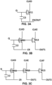
- FIGs. 3A through 3C show exemplary circuit diagrams of an output sub-circuit of the shift-register unit circuit according to some embodiments of the present disclosure not forming part of the claimed invention.
- the output sub-circuit 130 includes an output transistor M11 and an output capacitor C2.
- the output transistor M11 has a first terminal connected to a fourth clock-signal line CLKD, a second terminal connected to an output terminal CR/OUT, and a control terminal connected to the first node Q.
- the output capacitor C2 has a first terminal connected to the first node Q and a second terminal connected to the output terminal CR/OUT.
- the output capacitor C2 is configured to store and maintain the voltage level of the first node Q.
- the output transistor M11 When the voltage level of the first node Q is maintained at a high voltage level or turn-on voltage level, the output transistor M11 is turned on and output a signal from the fourth clock-signal line CLKD to the output terminal CR/OUT as an output signal.
- This output signal optionally is used as a driving signal for a pixel circuit, or optionally is used as a shift-register driving signal in a gate-driving circuit.
- the output sub-circuit 130 additionally includes two output terminals.
- the output sub-circuit 130 includes a first output transistor M11 and a second output transistor M13.
- the first output transistor M11 has a first terminal connected to the fourth clock-signal line CLKD, a second terminal connected to a first output terminal CR, and a control terminal connected to the first node Q.
- the second output transistor M13 has a first terminal connected to a fifth clock-signal line CLKE, a second terminal connected to a second output terminal OUT1, and a control terminal connected to the first node Q.
- an output signal outputted from the first output terminal CR can be used as a shift-register signal in a gate-driving circuit, while another output signal outputted from the second output terminal OUT1 can be used as a driving signal for driving a pixel circuit.
- the fourth clock-signal line CLKD and the fifth clock-signal line CLKE can be two different clock-signal lines or can be a same clock-signal line.
- the output sub-circuit 130 can includes multiple output terminals.
- the output sub-circuit 130 further includes a third output transistor M15 having a first terminal connected to a sixth clock-signal line CLKF, a second terminal connected to a third output terminal OUT2, and a control terminal connected to the first node Q.
- the sixth clock-signal line CLKF can be a same clock-signal line as the fourth clock-signal like CLKD or the fifth clock-signal line CLKF, or can be a different clock-signal line. It provides two different driving signals for a pixel circuit to enhance flexibility to drive the pixel circuit.
- the two output signals can be respectively used as driving signals for a scan transistor and a sense transistor.
- the two output signals can be respectively used as driving signals for a scan transistor and a sense transistor.
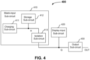
- FIG. 4 shows a block diagram of a shift-register unit circuit according to another embodiment of the present disclosure.
- the shift-register unit circuit 400 includes a blank-input sub-circuit 410, a display-input sub-circuit 420, and an output sub-circuit 430.
- the display-input sub-circuit 420 and the output sub-circuit 430 can be respective display-input sub-circuit 120 shown in FIG. 1 , FIG. 2A through FIG. 2E and output sub-circuit 130 shown in FIG. 3B through FIG. 3C .
- the blank-input sub-circuit 410 includes a charging sub-circuit 411, a storage sub-circuit 412, and an isolation sub-circuit 413.
- the charging sub-circuit 411 is configured to charge a blank-control node H based on a blank-input signal.
- the charging sub-circuit 411 receives the blank-input signal and provides a high-voltage blank-output-control signal or a blank-pull-up signal to the blank-control node H under control of the blank-input signal.
- the charging sub-circuit 411 is also configured, before an end of a blank period in one cycle of displaying one frame of image, to receive a first blank-reset signal and to reset the blank-control node H under control of the first blank-reset signal.
- the charging sub-circuit 411 is further configured to charge the blank-control node H based on a random input signal.
- the charging sub-circuit 411 receives a random input signal.
- a high-voltage blank-input signal can be inputted to the blank-control node H.
- the random input signal can be a random voltage pulse generated by a control unit circuit (not shown) such as a field programmable gate array (FPGA) or a microprocessor.
- the random input signal is an inputted voltage pulse in a random clock period during a display period in one cycle of displaying one frame of image.
- the storage sub-circuit 412 has one terminal connected to the blank-control node H and is configured to store a blank-control signal.
- the isolation sub-circuit 413 is configured to input the blank-output-control signal at the blank-control node H to the first node Q based on the blank-control signal stored at the storage sub-circuit 412.
- the isolation sub-circuit 413 is set between the first node Q and the blank-control node H and is used to prevent mutual interference between them. For example, when no need to output the blank-output-control signal, the isolation sub-circuit 413 can cut off the connection between the first node Q and the blank-control node H.
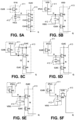
- FIG. 5A through FIG. 5H show various exemplary circuit diagrams of a blank-input sub-circuit of the shift-register unit circuit according to some embodiments of the present disclosure.
- the charging sub-circuit 411 includes a charging transistor M1 configured to charge the blank-control node H based on a blank-input signal from a blank-input terminal.
- the charging transistor M1 has a first terminal and/or control terminal connected to the blank-input terminal and a second terminal connected to the blank-control node H.
- the charging sub-circuit 411 is configured to input the blank-input signal to the blank-control node H, wherein figures 5B- 5H disclose embodiments not forming part of the claimed invention.
- the charging transistor M1 has a first terminal connected to the blank-input terminal STU1, a second terminal connected to the blank-control node H, and a control terminal connected to a second clock-signal line CLKB.
- the charging transistor M1 is turned on and allow a blank-input signal from the blank-input terminal STU1 to be inputted to the blank-control node H.
- the charging transistor M1 has its control terminal connected to its first terminal and commonly connected to the blank-input terminal STU1 and its second terminal connected to the blank-control node H.
- the charging transistor M1 is turned on to allow the turn-on voltage level of the blank-input signal to be passed to the blank-control node H.
- the charging sub-circuit 411 can be configured, under control of the blank-input signal, to input a blank-output-control signal at a turn-on voltage level to the blank-control node H.
- the charging transistor M1 has the first terminal connected to a high-voltage signal line VDD, the second terminal connected to the blank-control node H, and the control terminal connected to the blank-input terminal STU1.
- VDD high-voltage signal line
- the charging transistor M1 is turned on by a blank-input signal at the turn-on voltage level provided to the blank-input terminal STU1, a high-voltage signal from the VDD is passed as a blank-output-control signal to the blank-control node H.
- the charging sub-circuit 411 is configured to charge the blank-control node H based on a random input signal OE.
- the charging transistor M1 has a control terminal connected to a random-signal input terminal, a first terminal connected to an output terminal CR/OUT of a shift-register unit circuit, and a second terminal connected to the blank-control node H.
- the charging transistor M1 can connect its control terminal to a random signal input terminal and connect its first terminal to an output terminal CR ⁇ N-1> of a previous stage shift-register unit circuit in a same gate-driving circuit.
- the charging transistor M1 can connect its control terminal to an output terminal CR ⁇ N-1> of a previous stage shift-register unit circuit or an output terminal CR ⁇ N> of a current stage shift-register unit circuit, and connect its first terminal to a random signal input terminal.
- the charging sub-circuit 411 may be configured to input a blank-input signal to the blank-control node H based on a random input signal.
- a random signal input terminal in a shift-register unit circuit can randomly provide a high voltage signal during a display period in one cycle of displaying one frame of image.
- the charging transistor M1 under control of the random input signal at the high voltage level, is turned on.
- the high voltage signal can be inputted through M1 to the blank-control node H, i.e., to charge the blank-control node H.
- a shift-register unit circuit that is not outputting a high voltage level signal it is not going to charge the blank-control node H.
- the storage sub-circuit 412 includes a first capacitor C1 configured to store a blank-control signal.
- the first capacitor C1 has one terminal connected to the blank-control node H.
- the first capacitor C1 has a first terminal connected to the blank-control node H and a second terminal connected to a low voltage signal terminal VSS1 which inputs a turn-off voltage level signal.
- VSS1 low voltage signal terminal
- the charging sub-circuit 411 inputs a blank-output-control signal at the turn-on voltage level to the blank-control node, it also charges the first capacitor to maintain the voltage level at the blank-control node H to the turn-on voltage level.
- the first capacitor C1 has other ways of connection in the circuit in embodiments not forming part of the claimed invention.
- the first capacitor C1 has a first terminal connected to the blank-control node H and a second terminal connected to one terminal (e.g., a third clock-signal line CLKC) of the isolation sub-circuit 413.
- the first capacitor C1 has a first terminal connected to the blank-control node H and a second terminal connected to one terminal (e.g., a joint N connected between a first isolation transistor M3 and a second isolation transistor M4) of the isolation sub-circuit 413.
- the isolation sub-circuit 413 includes a first isolation transistor M3 and a second isolation transistor M4.
- the isolation sub-circuit 413 is configured to output the blank-output-control signal to the first node Q under control of the blank-control node H.
- the first isolation transistor M3 has a first terminal connected to the third clock-signal line CLKC, a second terminal connected to a first terminal of the second isolation transistor M4, and a control terminal connected to the blank-control node H.
- the second isolation transistor M4 has a second terminal connected to the first node Q and a control terminal connected to the third clock-signal line CLKC.
- the first isolation transistor M3 When the blank-control node H is maintained at a turn-on voltage level controlled by the storage sub-circuit 412, the first isolation transistor M3 is turned on by the turn-on voltage at the blank-control node H. If the third clock-signal line CLKC supplies a turn-on voltage level signal, the second isolation transistor M4 is turned on to allow the turn-on voltage level from the third clock-signal line CLKC to pass as a blank-output-control signal (or a blank-pull-up signal) to the first node Q.
- the first isolation transistor M3 has a first terminal connected to a high voltage signal line VDD.
- VDD high voltage signal line
- the first isolation transistor M3 is turned on. If the first clock-signal line CLKA supplies a turn-on voltage level signal to turn on the second isolation transistor M4, the turn-on voltage level from VDD can be passed as a blank-output-control signal (or a blank-pull-up signal) to the first node Q.
- FIG. 5A through FIG. 5H show a connection structure corresponding to each of odd stages shift-register unit circuits. If the second clock-signal line CLKB and the third clock-signal line CLKC in those circuits shown in FIG. 5A through FIG. 5H are interchanged, the corresponding connection structure is just fitted to each of even stages shift-register unit circuits.
- the isolation sub-circuit 413 is configured to output a turn-on voltage stored at the blank-control node H as the blank-output-control signal (or blank-pull-up signal) to the first node Q.
- the isolation sub-circuit 413 includes a first isolation transistor M3 having a first terminal connected to the blank-control node H, a second terminal connected to the first node Q, and a control terminal connected to the third clock-signal line CLKC.
- the first isolation transistor M3 When the third clock-signal line CLKC inputs a turn-on voltage level signal, the first isolation transistor M3 is turned on, and configured to input a blank-control signal at the turn-on voltage stored at the blank-control node H as the blank-output-control signal to the first node Q.
- the isolation sub-circuit 413 also includes a third isolation transistor M2 as shown in FIG. 5A .
- the third isolation transistor M2 is connected in series with the first isolation transistor M3 and the second isolation transistor M4.
- the third isolation transistor M2 has its control terminal connected to a first clock-signal line CLKA.
- the first clock-signal line provides a first clock signal for preventing a first node in a next stage shift-register unit circuit from being falsely written with a high voltage level to cause abnormal output due to a second clock signal from the second clock-signal line CLKB being at a high voltage level.
- the third isolation transistor M2 can be connected between M3 and M4.
- the third isolation transistor M2 can also be followed with M3 and M4 in series.
- the charging sub-circuit 411, the storage sub-circuit 412, and the isolation sub-circuit 413 can each have a plurality of different connection modes. Although only eight exemplary connections are illustrated in Figures 5A-5H , those skilled in the art will appreciate that the aforementioned charging sub-circuit 411, storage sub-circuit 412, and isolation sub-circuit 413 with arbitrary connection variations can be utilized in accordance with the principles of the present disclosure described above.
- FIG. 6 is a block diagram of a shift-register unit circuit according to yet another embodiment of the present disclosure.
- the shift-register unit circuit 600 includes a blank-input sub-circuit 410, a display-input sub-circuit 420, an output sub-circuit 430, a first control sub-circuit 440, a second control sub-circuit 450, a display-reset sub-circuit 460, and a blank-reset sub-circuit 470.
- the blank-input sub-circuit 410, the display-input sub-circuit 420, and the output sub-circuit 430 can be same one or variation of the blank-input sub-circuit 110/410 selected from those shown in FIG. 1 through FIG. 5H , or same one or variation of the display-input sub-circuit 120/420 thereof, or same one or variation of the output sub-circuit 130/430 thereof.
- the shift-register unit circuit 600 includes a first control sub-circuit 440 configured to control voltage level of a second node QB based on the first node Q. For example, when the first node Q is at a turn-on voltage level, the first control sub-circuit 440 can pull down the voltage level of the second node QB to a turn-off voltage level under control of the first node. In another example, when the first node is at a turn-off voltage level, the first control sub-circuit 440 is able to pull up the voltage level of the second node QB to a turn-on voltage level under control of the first node.
- the shift-register unit circuit 600 also includes a second control sub-circuit 450 configured to pull down the first node Q and the output terminal OUT to non-working voltage level under control of the second node QB. For example, when the output terminal OUT outputs no signal, it is configured to control the voltage level of the second node QB to pull down the first node Q and the output terminal to non-working voltage level so that noises at the output terminal of the shift-register unit circuit can be reduced.
- a second control sub-circuit 450 configured to pull down the first node Q and the output terminal OUT to non-working voltage level under control of the second node QB. For example, when the output terminal OUT outputs no signal, it is configured to control the voltage level of the second node QB to pull down the first node Q and the output terminal to non-working voltage level so that noises at the output terminal of the shift-register unit circuit can be reduced.
- the shift-register unit circuit 600 also includes a display-reset sub-circuit 460 configured to reset the first node Q under control of a display-reset signal.
- a display-reset sub-circuit 460 configured to reset the first node Q under control of a display-reset signal.
- the shift-register unit circuit 600 when it outputs a display-output signal in a display period of one cycle of displaying one frame of image, and right before an end of the display period, it is configured to receive the display-reset signal output by the display-reset sub-circuit 460 so as to pull down voltage level of the first node Q to a turn-off (low) voltage level.
- the shift-register unit circuit 600 also includes a blank-reset sub-circuit 470 configured to reset the first node Q and/or the output terminal OUT before an end of a blank period in one cycle of displaying one frame of image.
- a blank-reset sub-circuit 470 configured to reset the first node Q and/or the output terminal OUT before an end of a blank period in one cycle of displaying one frame of image.
- the shift-register unit circuit 600 outputs a blank-output signal during a blank period of the cycle, and right before an end of the blank period, it is configured to receive the blank-reset signal output by the blank-reset sub-circuit 470 so as to pull down a voltage level of the first node Q to a turn-off (low) voltage level.
- the blank-reset sub-circuit 470 is also configured to use the blank-reset sub-circuit 470 to pull down voltage level at the output terminal OUT to the turn-off (low) voltage level to reduce noises at the output terminal OUT of the shift-register unit circuit.
- one or more of the first control sub-circuit 440, the second control sub-circuit 450, the display-reset sub-circuit 460, and the blank-reset sub-circuit 470 can be selected to use or not in use depending on applications.
- the shift-register unit circuit of the present disclosure can achieve a function of controlling voltage level of a first node respectively by a blank-input sub-circuit and a display-input sub-circuit in different time periods of one cycle of displaying one frame of image.
- the shift-register unit circuit can achieve a function of using one output unit shared by the blank-input sub-circuit and the display-input sub-circuit to output a hybrid output signal.
- the shift-register unit circuit can control the voltage level of the first node during non-output time periods to reduce noise.
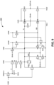
- FIG. 7 is an exemplary circuit diagram of a shift-register unit circuit according to a first embodiment of the present disclosure.
- the shift-register unit circuit 700 includes a blank-input sub-circuit 410, a display-input sub-circuit 420, and an output sub-circuit 430 substantially the same as those described herein. Additionally, the shift-register unit circuit 700 also includes a first control sub-circuit 440 including a first control transistor M7 with a control terminal and a first terminal commonly connected to a seventh clock-signal line CLKM and a second terminal connected to a second node QB.
- the seventh clock-signal line CLKM can provide a constant high-voltage (turn-on) signal.
- the first control sub-circuit 440 further includes a second control transistor M8 with a first terminal connected to the second node QB, a second terminal connected to a first signal line VGL1, and a control terminal connected to the first node Q.
- the first signal line VGL1 is optionally to input a low-voltage (turn-off) signal.
- the second control transistor M8 is turned on.
- the voltage level of the second node QB can be pulled down to a low voltage level.
- the second control transistor M8 is turned off.
- the high-voltage signal inputted to the seventh clock-signal line CLKM is passed to the second node QB, which pulls up the second node QB to a high voltage (turn-on) level.
- the seventh clock-signal line CLKM always supplies a high voltage signal during the operation of the shift-register unit circuit 700. Therefore, the first control transistor M7 is always in a conduction state, i.e., a turn-on state.
- the first control sub-circuit 440 also includes a third control transistor M10.
- the third control transistor M10 has a first terminal and a control terminal commonly connected to an eighth clock-signal line CLKN, and has a second terminal connected to the second node QB. As seen in FIG. 7 , the third control transistor M10 and the first control transistor M7 have a same structure in circuitry connection.
- the eighth clock-signal line inputs a low voltage signal.
- the first control transistor M7 is turned on while the third control transistor M10 is turned off.
- the eighth clock-signal line inputs a high voltage signal.
- the first control transistor M7 is turned off while the third control transistor M10 is turned on.
- the second control sub-circuit 450 includes a first pull-down transistor M9 with a first terminal connected to the first node Q, a second terminal connected to the first signal line VGL1, and a control terminal connected to the second node QB.
- the first signal line VGL1 is set to input a low-voltage turn-off signal.
- the second node QB is at a high voltage (turn-on) level
- the first pull-down transistor M9 is turned on to pull down a voltage level of the first node Q to a low voltage level.
- the second control sub-circuit 450 also includes a second pull-down transistor M12.
- the second pull-down transistor M12 has a first terminal connected to a first output terminal CR, a second terminal connected to the first signal line VGL1, and a control terminal connected to the second node QB. Again, the first signal line VGL1 is set to input a low voltage (turn-off) signal. When the second node is at a high voltage level, the second pull-down transistor M12 is turned on to pull down a voltage level of the first output terminal CR to a low voltage level.
- the second control sub-circuit further can include more pull-down transistors.
- the second control sub-circuit 450 includes a third pull-down transistor M14 having a first terminal connected to a second output terminal OUT, a second terminal connected to a second signal line VGL2, and a control terminal connected to the second node QB.
- the second signal line VGL2 is set to input a low voltage (turn-off) signal.
- the third pull-down transistor M14 is turned on to pull down the second output terminal OUT to a low voltage level.
- the display-reset sub-circuit 460 includes a display-reset transistor M6 having a first terminal connected to the first node Q, a second terminal connected to the first signal line VGL1, and a control terminal connected to a display-reset terminal STD2.
- the first signal line VGL1 is set to load a low voltage signal.
- the display-reset transistor M6 is turned on to pull down the first node Q to a low voltage level.
- the blank-reset sub-circuit 470 includes a first blank-reset transistor M15 having a first terminal connected to the first node Q, a second terminal connected to the first signal line VGL1, and a control terminal connected to a blank-reset terminal.
- the first signal line VGL1 is set to load a low voltage turn-off signal.
- the blank-reset terminal can provide a high-voltage turn-on signal to make the first blank-reset transistor being turned on and to pull down the first node Q to a low voltage level.
- the blank-reset sub-circuit 470 also includes a second blank-reset transistor (not shown in FIG.
- the second blank-reset transistor has a first terminal connected to a second clock-signal line CLKB, a second terminal connected to the first signal line VGL1, and a control terminal connected to the blank-reset terminal.
- the blank-reset terminal is connected to the second clock-signal line CLKB.
- a blank-reset signal and a second clock signal can be provided from a same signal line.
- the blank-reset signal can be provided by any signal lines shown in the figure or other separate signal line.
- the blank-reset terminal can be configured to be provided via a blank-reset control line TRST which can be configured to load a blank-reset signal before an end of one blank period of one cycle.
- This blank-reset signal is used to reset a voltage level of the first node Q so as to prevent generation of noise pulses at first node Q of other stages shift-register unit circuits cascaded in a same series of gate-driving circuit.
- first signal line VGL1 and the second signal line VGL2 shown in FIG. 7 can be a same signal line or two different signal lines.
- the signal lines can be arbitrarily set in the shift-register unit circuit in order to achieve proper operation or control of the transistors in the shift-register unit circuit.
- FIG. 8 shows an exemplary circuit diagram of a shift-register unit circuit according to a second embodiment of the present disclosure not forming part of the claimed invention.
- the shift-register unit circuit of the present disclosure it is possible to utilize a first capacitor C1 to maintain a voltage level at the blank-control node H and utilize a second capacitor C2 to maintain a voltage level at the first node Q.
- the first node Q and/or the blank-control node H are maintained at a turn-on voltage level, for some transistors having their first terminals connected to the first node Q and/or the blank-control node H and their second terminals connected to a signal line provided with a turn-off voltage level, there might be an issue of current leak due to the voltage difference between the first terminals and the respective second terminals even when their control terminals of the respective transistors is loaded with a turn-off signal.
- the current leak issue will cause the shift-register unit circuit performance degradation of maintaining voltage levels at the first node Q and/or the blank-control node H.
- the charging transistor M1 has a first terminal connected to a blank-input-signal line STU1, a second terminal connected to the blank-control node H.
- the charging transistor M1 can have current leak problem.
- the first node Q when the first node Q is set to a turn-on voltage level, the second signal line VGL2 is loaded with a low voltage signal, a current leak may occur at the transistor M6 and transistor M9.
- the shift-register unit circuit 800 includes an anti-leak sub-circuit 801.
- the anti-leak sub-circuit 801 can include a first anti-leak transistor M16 and one or more second anti-leak transistors M2, M6, M9. All the second anti-leak transistors (M2, M6, M9) have a first terminal connected to the first node Q, a second terminal connected to an anti-leak connection point OFF.
- the first anti-leak transistor M16 has its first terminal connected to a high-voltage signal line VDD and its second terminal connected to one terminal of all second anti-leak transistors (M2, M6, M9).
- the control terminal of M16 is connected to the first node Q.
- the first anti-leak transistor M16 is turned on to pass a high-voltage signal from the high-voltage signal line VDD to the first terminal of the second anti-leak transistor M2.
- Both the first terminal and the second terminal of the second anti-leak transistor M2 are set at high voltage level states, thereby preventing charges at the first node Q to leak through the second anti-leak transistor M2.
- the combination of the second anti-leak transistor M2 and the second isolation transistor M4 can achieve the same isolation function originally given by the isolation transistor as well as achieve a function of anti-leak.
- a combination of transistors M6 and M17 and another combination of transistors M9 and M18 also can achieve the functions of M6 and M9 in the corresponding shift-register unit circuit 700 and provide further an anti-leak function.
- FIG. 9 shows an exemplary circuit diagram of a shift-register unit circuit according to a third embodiment of the present disclosure.
- the second anti-leak transistor M2 in the shift-register unit circuit 900 has a control terminal connected to a first clock-signal line CLKA, not the third clock-signal line CLKC as shown in FIG. 8 .
- a first clock signal from the first clock-signal line CLKA is loaded with a low voltage level that is configured to be even lower than the turn-off voltage level provided in the third clock-signal line CLKC.
- the second isolation transistor M4 can have its control terminal configured to connect with the first clock-signal line CLKA.
- the second anti-leak transistor M2 can be configured to connect its control terminal to the third clock-signal line CLKC and the second isolation transistor M4 can be configured to connect its control terminal to the first clock-signal line CLKA to achieve a function of anti-leak in the shift-register unit circuit 900.
- FIG. 10 shows an exemplary circuit diagram of a shift-register unit circuit according to a fourth embodiment of the present disclosure not forming part of the claimed invention.
- the shift-register unit circuit 1000 can save an anti-leak transistor for the second isolation transistor M4, instead, the control terminal of the second isolation transistor M4 is connected to the first clock-signal line CLKA. Additionally, a first clock signal provided to the first clock-signal line CLKA is set to be lower than a third clock signal provided to the third clock-signal line CLKC. Under this configuration and voltage setting, it is able to prevent current leaking problem due to voltage rise induced by bootstrap effect at the first node Q.
- FIG. 11A through FIG. 11D show exemplary circuit diagrams of an anti-leak sub-circuit according to some embodiments of the present disclosure.
- a first anti-leak transistor M16 has a control terminal connected to an output terminal CR ⁇ N> or OUT ⁇ N> of a current-stage shift-register unit circuit.
- a first terminal of the first anti-leak transistor M16 is connected to a high voltage signal line VDD.
- a second terminal of the first anti-leak transistor M16 is connected to an anti-leak connection point OFF.
- a first anti-leak transistor M16 has a control terminal and a first terminal commonly connected to an output terminal CR ⁇ N> or OUT ⁇ N>.
- a second terminal of the first anti-leak transistor M16 is connected to an anti-leak connection point OFF.
- the first anti-leak transistor M16 shown in FIG. 11B and FIG. 11D can be turned on when the output sub-circuit has an output signal, then be able to prevent current leaking from the first node Q.
- the anti-leak sub-circuit shown in FIG. 11B and FIG. 11D can be used, when the first anti-leak transistor M16 is turned on by turn-on voltages at the output terminal CR ⁇ N> or OUT ⁇ N>, to prevent glitches in the output signal from being generated due to capacitance coupling in the circuit.
- FIG. 12 shows an exemplary circuit diagram of a shift-register unit circuit according to a fifth embodiment of the present d disclosure not forming part of the claimed invention.
- the shift-register unit circuit 1200 can also be configured to set an anti-leak circuitry structure in the charging sub-circuit.
- the shift-register unit circuit 1200 includes a first anti-leak sub-circuit 1201 including transistors M9_a, M10_a, M11_a, and M4_a. The functions of these transistors are similar to those transistors M6 and M9 in FIG. 10 .
- the first anti-leak transistor M16 shown in FIG. 10 is replaced by transistors M12_a and M12_b in FIG. 12 .
- the transistor M12_a has a control terminal connected to the first node Q, a first terminal connected to the high-voltage signal line VDD, and a second terminal connected to a first terminal and a control terminal of the transistor M12 b.
- the transistor M12 b also has a second terminal connected to an anti-leak connection point OFF.
- the shift-register unit circuit 1200 further includes a second anti-leak sub-circuit 1202 including a transistor M2_a, a transistor M2_b, and a transistor M1_b.
- the functions and connections of the transistors M2 a and M2 b are the same as the transistors M12 a and M12 b in the first anti-leak sub-circuit 1201.
- the transistor M1 b has same functions as transistors M9_a, M10_a, M11_a, and M4_a.
- the second anti-leak sub-circuit 1202 the current-leaking from the blank-control node H at high-voltage level via the charging transistor can be prevented.
- the anti-leak sub-circuit provided in the shift-register unit circuit of the present disclosure can prevent current-leaking due to existence of different voltage levels between the first node Q and the blank-control node H.
- the capacitors used in the shift-register unit circuit can be implemented directly with a stand-alone capacitor or can be parasitic capacitors associated with some transistors.
- FIG. 13 is a schematic block diagram of a gate-driving circuit according to a first embodiment of the present disclosure.
- the gate-driving circuit includes multiple shift-register unit circuit cascaded in multiple serial stages.
- each stage shift-register unit circuit can be substantially the same or a variation of circuitry structures of the shift-register unit circuits disclosed in FIG. 1 through FIG. 12 .
- an i-th stage shift-register unit circuit has a display input terminal STU2 and a blank-input terminal STU1, both being connected to an output terminal CR of a previous (i-1)-th stage shift-register unit circuit.
- the i-th stage shift-register unit circuit has an output terminal CR connected to a display-reset terminal STD2 of the previous (i-1)-th stage shift-register unit circuit.
- N is an integer greater than 2 and 1 ⁇ i ⁇ N.
- the first stage shift-register unit circuit has a display-input terminal STU2 connected directly to a display signal line and a blank-input terminal connected to a blank signal line.
- the N-th stage shift-register unit circuit has a display-reset terminal STD2 connected to a display-reset signal line.
- each stage shift-register unit circuit is connected to respective clock-signal lines and signal lines for providing all turn-on voltage signals or turn-off voltage signals just like those shown in FIG. 1 through FIG. 12 .
- FIG. 13 as a simplified schematic diagram does not show other signal lines connected to respective stages shift-register unit circuits.
- FIG. 14 is a schematic block diagram of a gate-driving circuit according to a second embodiment of the present disclosure not forming part of the claimed invention.
- the i-th stage shift-register unit circuit includes a blank-input terminal connected to an output terminal of the (i-1)-th stage shift-register unit circuit.
- the i-th stage shift-register unit circuit also includes a display-input terminal connected to an output terminal of the (i-2)-th stage shift-register unit circuit.
- the i-th stage shift-register unit circuit further includes a display-reset terminal connected to an output terminal of the (i+2)-th stage shift-register unit circuit.
- the first stage shift-register unit circuit has its blank-input terminal and display-input terminal respectively connected with a blank-input signal line and a first display-input signal line.
- the second stage shift-register unit circuit has it display-input terminal connected to a second display-input signal line.
- the (N-1)-th stage shift-register unit circuit has its display-reset terminal connected to a first display-reset signal line.
- the N-th stage shift-register unit circuit has its display-reset terminal connected to a first display-reset signal line.
- Each stage of the multi-stage cascaded shift-register unit circuits is connected to a first clock-signal line CLKA, a second clock-signal line CLKB, a third clock-signal line CLKC, and a respective one of fourth clock-signal lines CLKD_1, CLKD_2, CLKD_3, and CLKD_4.
- the odd-stage shift-register unit circuit and the even-stage shift-register unit circuit have their second clock-signal line CLKB and third clock-signal line CLKC being setup alternately in order.
- FIG. 14 is merely an example showing different clock-signal lines. There can be many structure variations in respective stages shift-register unit circuits which may respectively connect to different clock-signal lines depending on specific applications.
- FIG. 15 shows a timing diagram of driving a gate-driving circuit according to an embodiment of the present disclosure not forming part of the claimed invention.
- the timing diagram of FIG. 15 can be applied to drive the gate-driving circuit of FIG. 14 .
- the blank-input terminal STU1 and the display-input terminal STU2 all are inputted with an input signal STU.
- clock-signal lines CLKD_1, CLKD_2, CLKD_3, and CLKD_4 represent four fourth clock-signal lines connected respectively to a first, second, third, and fourth stage shift-register unit circuits.
- Q ⁇ 1> and Q ⁇ 2> represent voltages of a first node Q in respective first and second stage shift-register unit circuits.
- OUT ⁇ 1>, OUT ⁇ 2>, OUT ⁇ 3>, and OUT ⁇ 4> represent voltages at output terminals CR and OUT of respective first, second, third, and fourth stage shift-register unit circuits.
- one of a seventh clock-signal line CLKM and an eighth clock-signal line CLKN inputs a high-voltage turn-on signal while the other one inputs a low-voltage turn-off signal. Therefore, a corresponding second node QB is maintained at a high-voltage level and a corresponding first node Q is maintained at a low-voltage level.
- each of the second clock-signal like CLKB and the third clock-signal line CLKC inputs a high-voltage level turn-on signal.
- the first stage shift-register unit circuit receives a high-voltage signal as display-input from its display-input terminal STU2.
- the display-input sub-circuit of the shift-register unit circuit can output a display-pull-up signal to the first node Q based on the display-input signal (at the turn-on voltage level) and pull up the voltage level of the first node Q to a high voltage level.
- the output sub-circuit receives a high-voltage input signal from the fourth clock-signal CLKD_1 of the first stage shift-register unit circuit. Since output transistors M11 and M13 are turned on by the high voltage at the first node Q, the high-voltage input signal from the fourth clock-signal line can be outputted as output signal to the output terminals CR and OUT_1H through the output transistors M11 and M13.
- the second clock-signal line CLKB also inputs a high-voltage turn-on signal
- a charging transistor of the first stage shift-register unit circuit is turned on by the turn-on signal from the CLKB, and also can pass the high-voltage signal inputted from the input terminal STU to a corresponding blank-control node H to charge the node H.
- the second stage shift-register unit circuit For the second stage shift-register unit circuit, its second display-input terminal STU2_2 receives the high-voltage input signal STU as a display-input signal.
- the display-input sub-circuit of the second stage shift-register unit circuit outputs a display-pull-up signal to the first node Q based on the display-input signal to pull up the first node Q to a high voltage level. Then, the output sub-circuit of the second stage shift-register unit circuit receives a high-voltage input signal from the fourth clock-signal line CLKD_2.
- the high-voltage input signal from the fourth clock-signal line CLKD_2 can pass through the output transistors M11 and M13 to be output at the output terminals CR and OUT_1H.
- the charging transistor of the second stage shift-register unit circuit receives a blank-output signal from the first stage shift-register unit circuit.
- the odd-stage shift-register unit circuit and the even-stage shift-register unit circuit have their second clock-signal line CLKB and third clock-signal line CLKC being setup alternately in order.
- the third clock-signal line CLKC inputs a high-voltage level signal in the blank period.
- the blank-control node H of the second stage shift-register unit circuit is pulled up to a high voltage level. And so on, each stage shift-register unit circuit outputs a respective blanking-output signal like this.
- the fourth clock-signal line CLKD_2 that connects to the second stage shift-register unit circuit inputs a second clock signal having a same pulse width as a first clock signal inputted from the fourth clock-signal line CLKD_1 that connects to the first stage shift-register unit circuit.
- the second clock signal has a rising edge delayed by half of the pulse wide compared to the first clock signal.
- a display-input signal outputted by the second stage shift-register unit circuit is also delayed by half a pulse width than the display-input signal outputted by the first stage shift-register unit circuit.
- a display-output signal of the first stage shift-register unit circuit and a display-output signal of the second stage shift-register unit circuit have 50% pulse overlap.
- a display-output signal from the first stage shift-register unit circuit can be used as a display-input signal of the third stage shift-register unit circuit
- all odd stages shift-register unit circuits will output respective display-output signals based on that of the first stage shift-register unit circuit.
- all even stages shift-register unit circuits will output respective display-output signals based on that of the first stage shift-register unit circuit with 50% overlapping with that of display-output signals of respective previous odd stages shift-register unit circuits.
- the first clock-signal line CLKA and the third clock-signal line CLKC input high-voltage turn-on signals to use the blank-input sub-circuit to charge the first node Q.
- the fourth clock-signal line CLKD_1 connected with the first stage shift-register unit circuit inputs a high-voltage turn-on signal and controls the output sub-circuit to output a blank-output signal.
- the second clock-signal line CLKB After outputting the blank-output signal and before the end of the blank period, the second clock-signal line CLKB again inputs a high-voltage turn-on signal. Since at this time the blank-input terminals of all odd stages shift-register unit circuits are at a low-voltage level, the charging transistors of all odd stages shift-register unit circuits are turned on by the high voltage signal from the second clock-signal line CLKB to discharge the blank-control node H. Effectively, the blank-control node H is reset (to a low voltage level) before an end of the cycle of displaying one frame of image. This reduces the time of put the blank-control node H at the high-voltage level, avoiding the transistor performance degradation due to being in conduction state for too long.
- the third clock-signal line CLKC can be used to input a high voltage turn-on signal after outputting an blank-output signal and before the end of the blank period.
- the blank-input terminals of all even stages shift-register unit circuits are set to a low voltage level.
- the charging transistors of all even stage shift-register unit circuits are turned on by the high voltage turn-on signal from the third clock-signal line CLKC to discharge the blank-control node H through the respective charging transistors.
- the gate-driving circuit of FIG. 14 is configured to output display-output signals with 50% overlap pulse timing between two neighboring stages shift-register unit circuits.
- the gate-driving circuit of the present disclosure can also be configured to output display-output signals with other percentage of overlap in pulse timing depending on applications.
- the gate-driving circuit based on N-stages cascaded shift-register unit circuits can be divided to multiple groups.
- the gate-driving circuit includes m groups.
- Each group includes n shift-register unit circuits with each of them being those shift-register unit circuits described herein.
- the n shift-register unit circuits of each group are connected stage-by-stage to respective n shift-register unit circuits of a next group.
- an output terminal of a first shift-register unit circuit of a first group is connected to a display-input terminal of a first shift-register unit circuit of a second group (which can also be viewed as the (n+1)-th stage shift-register unit circuit of the N-stage cascaded shift-register unit circuits).
- An output terminal of a second shift-register unit circuit of the first group is connected to a display-input terminal of the second shift-register unit circuit of the second group, and so on.
- the gate-driving circuit is configured to have a display-output signal from each stage shift-register unit circuit to be overlapped with another display-output signal of a next stage shift-register unit circuit by 1/n pulse in time-domain.
- the display-output signals of the gate-driving circuit adopt odd-stage cascaded configuration alternately combined with even-stage cascaded configuration to achieve display-output signals from neighboring stages with 50% pulse overlap.
- the gate-driving circuit adopting 1, 4, 7, ... stage cascaded configuration alternately combined with 2, 5, 8, ... stage cascaded configuration plus 3, 6, 9, ... stage cascaded configuration, the display-output signals from neighboring stages will have 33% pulse overlap.
- other variations and modifications can be implemented to achieve different percentages of pulse overlapping for the display-output signals from neighboring stages shift-register unit circuits.
- the blank-input terminals of the N-stage cascaded shift-register unit circuits are also configured to be configured via cascaded connections among different stages.
- an output terminal of the first stage shift-register unit circuit is connected to a blank-input terminal of the second stage shift-register unit circuit.
- An output terminal of the second stage shift-register unit circuit is connected to a blank-input terminal of the third stage shift-register unit circuit, and so on.
- FIG. 16 is a schematic block diagram of a gate-driving circuit according to a third embodiment of the present disclosure not forming part of the claimed invention.
- N is a positive integer.
- the i-th stage shift-register unit circuit has a blank-input terminal connected to an output terminal of the (i-1)-th stage shift-register unit circuit.
- the i-th stage shift-register unit circuit has a display-input terminal connected to an output terminal of the (i-2)-th stage shift-register unit circuit.
- the i-th stage shift-register unit circuit has a display-reset terminal connected to an output terminal of the (i+3)-th stage shift-register unit circuit.
- the first stage shift-register unit circuit has a blank-input terminal and a display-input terminal respectively connected to a blank-input signal line and a first display-input signal line.
- the second stage shift-register unit circuit has a display-input terminal connected to a second display-input signal line.
- the (N-2)-th stage shift-register unit circuit has a display-reset terminal connected to a first display-reset signal line.
- the (N-1)-th stage shift-register unit circuit has a display-reset terminal connected to a second display-reset signal line.
- the N-th stage shift-register unit circuit has a display-reset terminal connected to a third display-reset signal line.
- the gate-driving circuit of FIG. 16 has some major differences versus the gate-driving circuit of FIG. 14 .
- the i-th stage shift-register unit circuit has an output terminal connected to a display-input terminal of (i+2)-th stage shift-register unit circuit.
- the (i+2)-th stage shift-register unit circuit has an output terminal connected to the display-reset terminal of the i-th stage shift-register unit circuit.
- the output terminal OUT of each shift-register unit circuit is to output a gate-driving signal for driving a pixel circuit.
- an output transistor M13 with large-volume id adopted therein Accordingly, in a display-reset period of one cycle of displaying one frame of image, the output terminal OUT may accumulate charges which can be reset through a display-reset transistor M14 with relatively large volume.
- the accumulated charges at the output terminal OUT can be discharged through output transistor M13 without need to be reset through the display-reset transistor M14.
- the display-reset transistor M14 can adopt a smaller volume transistor, further reducing the volume of each shift-register unit circuit. Additionally, because that the voltage level of the first node Q can be raised through a bootstrap effect when the output terminal of the output sub-circuit is at a high-voltage level, the current that flows through the output transistor M13 during discharging can be even larger, making the discharging process faster in the shift-register unit circuit according to some embodiments of the present disclosure.
- the present disclosure provides a display apparatus including a gate-driving circuit described herein.
- the display apparatus includes one selected from a smart phone, a tablet computer, a television, a displayer, a notebook computer, a digital-picture frame, a navigator, and any product of component having a display function.
- FIG. 17 shows a flow chart showing a method for driving a shift-register unit circuit according to an embodiment of the present disclosure.
- the driving method 1700 includes a step of 1701: in a control period or a first pull-up period, a display output-control signal is inputted through a display-input sub-circuit to a first node in the shift-register unit circuit. Additionally, the driving method 1700 also includes a step of 1702: in a first output period, a display-output signal is outputted through an output sub-circuit under control of the display output-control signal at the first node.
- the driving method 1700 includes a step of 1703: in a second control period or a second pull-up period, a blank output-control signal is inputted via an isolation sub-circuit based on a blank-control signal to the first node through a blank-input sub-circuit in the shift-register unit circuit. Furthermore, the driving method 1700 includes a step of 1704: in a second output period, a blank-output signal is outputted via the output sub-circuit under control of the blank-output-control signal at the first node. Moreover, the driving method 1700 includes a step of 1705: in a first blank-reset period, a blank-control node of the shift-register unit circuit is reset under control of a first blank-reset signal.
- the driving method 1700 also includes a step of 1702B: in a display-reset period, the first node in the shift-register unit circuit is reset to a low voltage level under control of a display-reset signal.
- the driving method 1700 also includes a step of 1703B: in the blank period, an anti-leak sub-circuit is to provide a working voltage level to maintain between the first node and the blank-control node.
- the driving method 1700 also includes a step of 1705B: in a first blank-reset period, the blank-control node in the shift-register unit circuit is reset to a low voltage level under control of a first blank-reset signal.
- the method is provided to reset the blank-input sub-circuit before an end of a blank period so that the time for transistors in the blank-input sub-circuit in a conduction state can be reduced, so can be transistor performance degradation due to long time stress.
Landscapes
- Engineering & Computer Science (AREA)
- Physics & Mathematics (AREA)
- Computer Hardware Design (AREA)
- General Physics & Mathematics (AREA)
- Theoretical Computer Science (AREA)
- Control Of Indicators Other Than Cathode Ray Tubes (AREA)
- Liquid Crystal Display Device Control (AREA)
- Shift Register Type Memory (AREA)
- Control Of El Displays (AREA)
Applications Claiming Priority (2)
| Application Number | Priority Date | Filing Date | Title |
|---|---|---|---|
| CN201810852379.7A CN109935200B (zh) | 2018-07-27 | 2018-07-27 | 移位寄存器单元、栅极驱动电路、显示装置以及驱动方法 |
| PCT/CN2019/093721 WO2020019936A1 (en) | 2018-07-27 | 2019-06-28 | Shift-register unit circuit, gate-driving circuit, display apparatus, and driving method |
Publications (3)
| Publication Number | Publication Date |
|---|---|
| EP3830817A1 EP3830817A1 (en) | 2021-06-09 |
| EP3830817A4 EP3830817A4 (en) | 2022-05-11 |
| EP3830817B1 true EP3830817B1 (en) | 2024-11-20 |
Family
ID=66984462
Family Applications (1)
| Application Number | Title | Priority Date | Filing Date |
|---|---|---|---|
| EP19839244.1A Active EP3830817B1 (en) | 2018-07-27 | 2019-06-28 | Shift-register unit circuit, gate-driving circuit, display apparatus, and driving method |
Country Status (5)
| Country | Link |
|---|---|
| US (4) | US11468810B2 (https=) |
| EP (1) | EP3830817B1 (https=) |
| JP (2) | JP7374170B2 (https=) |
| CN (2) | CN114822393B (https=) |
| WO (1) | WO2020019936A1 (https=) |
Families Citing this family (14)
| Publication number | Priority date | Publication date | Assignee | Title |
|---|---|---|---|---|
| CN109935208B (zh) * | 2018-02-14 | 2021-03-02 | 京东方科技集团股份有限公司 | 移位寄存器单元、栅极驱动电路、显示装置以及驱动方法 |
| CN114822393B (zh) * | 2018-07-27 | 2024-03-15 | 京东方科技集团股份有限公司 | 移位寄存器单元、栅极驱动电路、显示装置以及驱动方法 |
| CN109935204B (zh) * | 2019-01-18 | 2022-06-03 | 合肥京东方卓印科技有限公司 | 移位寄存器单元、栅极驱动电路、显示装置及驱动方法 |
| CN112447133B (zh) * | 2019-08-30 | 2022-05-20 | 京东方科技集团股份有限公司 | 移位寄存器及其驱动方法、栅极驱动电路、显示面板 |
| CN110534051A (zh) * | 2019-09-26 | 2019-12-03 | 京东方科技集团股份有限公司 | 移位寄存器单元、驱动方法、栅极驱动电路及显示装置 |
| CN111261116B (zh) * | 2020-04-02 | 2021-05-25 | 合肥京东方卓印科技有限公司 | 移位寄存器单元及其驱动方法、栅极驱动电路、显示装置 |
| CN112185297B (zh) * | 2020-10-26 | 2023-12-05 | 京东方科技集团股份有限公司 | 栅极驱动单元、栅极驱动方法,栅极驱动电路和显示装置 |
| US11837133B2 (en) * | 2021-01-28 | 2023-12-05 | Boe Technology Group Co., Ltd. | Gate driving circuit, method of driving gate driving circuit, and display panel |
| CN113112949B (zh) * | 2021-04-27 | 2023-06-30 | 武汉天马微电子有限公司 | 一种栅极驱动电路、显示面板、显示装置及驱动方法 |
| CN113781967B (zh) * | 2021-09-27 | 2023-01-24 | 合肥京东方卓印科技有限公司 | 移位寄存器单元及其驱动方法、栅极驱动电路和显示装置 |
| US12230340B2 (en) | 2021-11-30 | 2025-02-18 | Boe Technology Group Co., Ltd. | Shift register unit, gate driving circuit and display device |
| WO2023178701A1 (zh) * | 2022-03-25 | 2023-09-28 | 京东方科技集团股份有限公司 | 移位寄存器、扫描驱动电路及显示装置 |
| CN116229862B (zh) * | 2022-12-30 | 2026-03-31 | 惠科股份有限公司 | 电路驱动方法及显示装置 |
| KR20250052564A (ko) * | 2023-10-11 | 2025-04-21 | 삼성디스플레이 주식회사 | 게이트 구동부 및 이를 포함하는 표시 장치 |
Family Cites Families (28)
| Publication number | Priority date | Publication date | Assignee | Title |
|---|---|---|---|---|
| JP2004350058A (ja) | 2003-05-22 | 2004-12-09 | Handotai Rikougaku Kenkyu Center:Kk | 電源スイッチ回路 |
| JP4993544B2 (ja) | 2005-03-30 | 2012-08-08 | 三菱電機株式会社 | シフトレジスタ回路 |
| KR20100006063A (ko) * | 2008-07-08 | 2010-01-18 | 삼성전자주식회사 | 게이트 드라이버 및 이를 갖는 표시장치 |
| RU2532702C2 (ru) | 2009-11-13 | 2014-11-10 | Панасоник Интеллекчуал Проперти Корпорэйшн оф Америка | Способ кодирования, способ декодирования, кодер и декодер |
| WO2013042622A1 (ja) * | 2011-09-22 | 2013-03-28 | シャープ株式会社 | 表示装置およびその駆動方法 |
| KR102091485B1 (ko) * | 2013-12-30 | 2020-03-20 | 엘지디스플레이 주식회사 | 유기 발광 표시 장치 및 그의 구동 방법 |
| KR102128579B1 (ko) | 2014-01-21 | 2020-07-01 | 삼성디스플레이 주식회사 | 게이트 구동 회로 및 이를 구비한 표시 장치 |
| CN103943083B (zh) | 2014-03-27 | 2017-02-15 | 京东方科技集团股份有限公司 | 一种栅极驱动电路及其驱动方法、显示装置 |
| KR102268965B1 (ko) * | 2014-12-04 | 2021-06-24 | 엘지디스플레이 주식회사 | 게이트 쉬프트 레지스터 및 이를 이용한 표시 장치 |
| CN104464605B (zh) * | 2014-12-30 | 2017-12-08 | 上海中航光电子有限公司 | 一种移位寄存器及其驱动方法、栅极驱动电路及显示屏 |
| US9818338B2 (en) * | 2015-03-04 | 2017-11-14 | Texas Instruments Incorporated | Pre-charge driver for light emitting devices (LEDs) |
| CN104732940B (zh) | 2015-03-30 | 2017-03-15 | 深圳市华星光电技术有限公司 | Cmos栅极驱动电路 |
| CN104835476B (zh) * | 2015-06-08 | 2017-09-15 | 京东方科技集团股份有限公司 | 移位寄存器单元、栅极驱动电路及其驱动方法、阵列基板 |
| CN105118459B (zh) * | 2015-09-17 | 2017-09-26 | 深圳市华星光电技术有限公司 | 一种goa电路及液晶显示器 |
| KR102635475B1 (ko) * | 2015-12-29 | 2024-02-08 | 엘지디스플레이 주식회사 | 게이트 쉬프트 레지스터와 이를 포함한 유기발광 표시장치 및 그 구동방법 |
| CN105741742B (zh) | 2016-05-09 | 2019-05-14 | 京东方科技集团股份有限公司 | 一种移位寄存器单元、栅极驱动电路及其驱动方法 |
| CN106023943A (zh) * | 2016-08-02 | 2016-10-12 | 京东方科技集团股份有限公司 | 移位寄存器及其驱动方法、栅极驱动电路和显示装置 |
| KR102578838B1 (ko) * | 2016-09-30 | 2023-09-18 | 엘지디스플레이 주식회사 | 게이트 구동부 및 이를 포함하는 표시장치 |
| CN106486049B (zh) * | 2017-01-04 | 2017-10-31 | 京东方科技集团股份有限公司 | 移位寄存器单元、驱动方法、goa电路和显示装置 |
| CN106548747A (zh) * | 2017-02-06 | 2017-03-29 | 京东方科技集团股份有限公司 | 移位寄存器单元及其驱动方法、栅极驱动电路及显示装置 |
| CN106847221A (zh) * | 2017-03-20 | 2017-06-13 | 京东方科技集团股份有限公司 | 移位寄存器单元、栅极驱动电路以及驱动方法 |
| KR102338948B1 (ko) * | 2017-05-22 | 2021-12-14 | 엘지디스플레이 주식회사 | 게이트 쉬프트 레지스터와 이를 포함한 유기발광 표시장치 |
| CN107516505B (zh) * | 2017-10-19 | 2021-01-15 | 京东方科技集团股份有限公司 | 移位寄存器单元及其驱动方法、栅极驱动电路和显示面板 |
| CN108122529B (zh) * | 2018-01-25 | 2021-08-17 | 京东方科技集团股份有限公司 | 栅极驱动单元及其驱动方法和栅极驱动电路 |
| CN109935196B (zh) * | 2018-02-14 | 2020-12-01 | 京东方科技集团股份有限公司 | 移位寄存器单元、栅极驱动电路、显示装置以及驱动方法 |
| CN108281123B (zh) | 2018-03-30 | 2020-03-10 | 京东方科技集团股份有限公司 | 移位寄存器单元、栅极驱动电路、显示装置以及驱动方法 |
| CN114677965B (zh) | 2018-05-31 | 2023-12-26 | 京东方科技集团股份有限公司 | 移位寄存器单元、栅极驱动电路及显示装置 |
| CN114822393B (zh) * | 2018-07-27 | 2024-03-15 | 京东方科技集团股份有限公司 | 移位寄存器单元、栅极驱动电路、显示装置以及驱动方法 |
-
2018
- 2018-07-27 CN CN202210460044.7A patent/CN114822393B/zh active Active
- 2018-07-27 CN CN201810852379.7A patent/CN109935200B/zh active Active
-
2019
- 2019-06-28 EP EP19839244.1A patent/EP3830817B1/en active Active
- 2019-06-28 WO PCT/CN2019/093721 patent/WO2020019936A1/en not_active Ceased
- 2019-06-28 US US16/612,947 patent/US11468810B2/en active Active
- 2019-06-28 JP JP2021502420A patent/JP7374170B2/ja active Active
-
2022
- 2022-08-11 US US17/819,215 patent/US11769437B2/en active Active
-
2023
- 2023-08-20 US US18/452,552 patent/US12183237B2/en active Active
- 2023-10-24 JP JP2023182244A patent/JP7588696B2/ja active Active
-
2024
- 2024-10-23 US US18/924,166 patent/US20250046224A1/en active Pending
Also Published As
| Publication number | Publication date |
|---|---|
| US20220383792A1 (en) | 2022-12-01 |
| EP3830817A1 (en) | 2021-06-09 |
| US20210358366A1 (en) | 2021-11-18 |
| JP2024010076A (ja) | 2024-01-23 |
| CN109935200B (zh) | 2022-06-03 |
| US11468810B2 (en) | 2022-10-11 |
| US20230395010A1 (en) | 2023-12-07 |
| WO2020019936A1 (en) | 2020-01-30 |
| CN114822393B (zh) | 2024-03-15 |
| CN114822393A (zh) | 2022-07-29 |
| JP7588696B2 (ja) | 2024-11-22 |
| US11769437B2 (en) | 2023-09-26 |
| US20250046224A1 (en) | 2025-02-06 |
| JP7374170B2 (ja) | 2023-11-06 |
| CN109935200A (zh) | 2019-06-25 |
| EP3830817A4 (en) | 2022-05-11 |
| JP2021531500A (ja) | 2021-11-18 |
| US12183237B2 (en) | 2024-12-31 |
Similar Documents
| Publication | Publication Date | Title |
|---|---|---|
| EP3830817B1 (en) | Shift-register unit circuit, gate-driving circuit, display apparatus, and driving method | |
| US11769457B2 (en) | Shift register unit set, gate driving circuit and display apparatus | |
| US12518671B2 (en) | Shift register, gate driving circuit, display apparatus and driving method | |
| KR102551784B1 (ko) | 시프트 레지스터 유닛과 그 구동 방법, 게이트 구동 회로 및 디스플레이 디바이스 | |
| CN109935209B (zh) | 移位寄存器单元、栅极驱动电路、显示装置及驱动方法 | |
| CN109935199B (zh) | 移位寄存器单元、栅极驱动电路、显示装置及驱动方法 | |
| US12087198B2 (en) | Shift register, gate driving circuit, display apparatus and driving method | |
| CN112639947A (zh) | 移位寄存器单元及驱动方法、栅极驱动电路和显示装置 |
Legal Events
| Date | Code | Title | Description |
|---|---|---|---|
| STAA | Information on the status of an ep patent application or granted ep patent |
Free format text: STATUS: UNKNOWN |
|
| STAA | Information on the status of an ep patent application or granted ep patent |
Free format text: STATUS: THE INTERNATIONAL PUBLICATION HAS BEEN MADE |
|
| PUAI | Public reference made under article 153(3) epc to a published international application that has entered the european phase |
Free format text: ORIGINAL CODE: 0009012 |
|
| STAA | Information on the status of an ep patent application or granted ep patent |
Free format text: STATUS: REQUEST FOR EXAMINATION WAS MADE |
|
| 17P | Request for examination filed |
Effective date: 20200129 |
|
| AK | Designated contracting states |
Kind code of ref document: A1 Designated state(s): AL AT BE BG CH CY CZ DE DK EE ES FI FR GB GR HR HU IE IS IT LI LT LU LV MC MK MT NL NO PL PT RO RS SE SI SK SM TR |
|
| DAV | Request for validation of the european patent (deleted) | ||
| DAX | Request for extension of the european patent (deleted) | ||
| REG | Reference to a national code |
Ref country code: DE Ref legal event code: R079 Free format text: PREVIOUS MAIN CLASS: G09G0003320800 Ipc: G09G0003326600 Ref document number: 602019062341 Country of ref document: DE |
|
| A4 | Supplementary search report drawn up and despatched |
Effective date: 20220411 |
|
| RIC1 | Information provided on ipc code assigned before grant |
Ipc: G11C 19/28 20060101ALI20220405BHEP Ipc: G09G 3/3266 20160101AFI20220405BHEP |
|
| STAA | Information on the status of an ep patent application or granted ep patent |
Free format text: STATUS: EXAMINATION IS IN PROGRESS |
|
| 17Q | First examination report despatched |
Effective date: 20230123 |
|
| GRAP | Despatch of communication of intention to grant a patent |
Free format text: ORIGINAL CODE: EPIDOSNIGR1 |
|
| STAA | Information on the status of an ep patent application or granted ep patent |
Free format text: STATUS: GRANT OF PATENT IS INTENDED |
|
| INTG | Intention to grant announced |
Effective date: 20240726 |
|
| GRAS | Grant fee paid |
Free format text: ORIGINAL CODE: EPIDOSNIGR3 |
|
| GRAA | (expected) grant |
Free format text: ORIGINAL CODE: 0009210 |
|
| STAA | Information on the status of an ep patent application or granted ep patent |
Free format text: STATUS: THE PATENT HAS BEEN GRANTED |
|
| AK | Designated contracting states |
Kind code of ref document: B1 Designated state(s): AL AT BE BG CH CY CZ DE DK EE ES FI FR GB GR HR HU IE IS IT LI LT LU LV MC MK MT NL NO PL PT RO RS SE SI SK SM TR |
|
| REG | Reference to a national code |
Ref country code: GB Ref legal event code: FG4D |
|
| REG | Reference to a national code |
Ref country code: CH Ref legal event code: EP |
|
| REG | Reference to a national code |
Ref country code: DE Ref legal event code: R096 Ref document number: 602019062341 Country of ref document: DE |
|
| REG | Reference to a national code |
Ref country code: IE Ref legal event code: FG4D |
|
| REG | Reference to a national code |
Ref country code: LT Ref legal event code: MG9D |
|
| REG | Reference to a national code |
Ref country code: NL Ref legal event code: MP Effective date: 20241120 |
|
| PG25 | Lapsed in a contracting state [announced via postgrant information from national office to epo] |
Ref country code: PT Free format text: LAPSE BECAUSE OF FAILURE TO SUBMIT A TRANSLATION OF THE DESCRIPTION OR TO PAY THE FEE WITHIN THE PRESCRIBED TIME-LIMIT Effective date: 20250320 Ref country code: HR Free format text: LAPSE BECAUSE OF FAILURE TO SUBMIT A TRANSLATION OF THE DESCRIPTION OR TO PAY THE FEE WITHIN THE PRESCRIBED TIME-LIMIT Effective date: 20241120 Ref country code: IS Free format text: LAPSE BECAUSE OF FAILURE TO SUBMIT A TRANSLATION OF THE DESCRIPTION OR TO PAY THE FEE WITHIN THE PRESCRIBED TIME-LIMIT Effective date: 20250320 |
|
| PG25 | Lapsed in a contracting state [announced via postgrant information from national office to epo] |
Ref country code: NL Free format text: LAPSE BECAUSE OF FAILURE TO SUBMIT A TRANSLATION OF THE DESCRIPTION OR TO PAY THE FEE WITHIN THE PRESCRIBED TIME-LIMIT Effective date: 20241120 Ref country code: FI Free format text: LAPSE BECAUSE OF FAILURE TO SUBMIT A TRANSLATION OF THE DESCRIPTION OR TO PAY THE FEE WITHIN THE PRESCRIBED TIME-LIMIT Effective date: 20241120 |
|
| REG | Reference to a national code |
Ref country code: AT Ref legal event code: MK05 Ref document number: 1744326 Country of ref document: AT Kind code of ref document: T Effective date: 20241120 |
|
| PG25 | Lapsed in a contracting state [announced via postgrant information from national office to epo] |
Ref country code: BG Free format text: LAPSE BECAUSE OF FAILURE TO SUBMIT A TRANSLATION OF THE DESCRIPTION OR TO PAY THE FEE WITHIN THE PRESCRIBED TIME-LIMIT Effective date: 20241120 |
|
| PG25 | Lapsed in a contracting state [announced via postgrant information from national office to epo] |
Ref country code: ES Free format text: LAPSE BECAUSE OF FAILURE TO SUBMIT A TRANSLATION OF THE DESCRIPTION OR TO PAY THE FEE WITHIN THE PRESCRIBED TIME-LIMIT Effective date: 20241120 |
|
| PG25 | Lapsed in a contracting state [announced via postgrant information from national office to epo] |
Ref country code: NO Free format text: LAPSE BECAUSE OF FAILURE TO SUBMIT A TRANSLATION OF THE DESCRIPTION OR TO PAY THE FEE WITHIN THE PRESCRIBED TIME-LIMIT Effective date: 20250220 |
|
| PG25 | Lapsed in a contracting state [announced via postgrant information from national office to epo] |
Ref country code: GR Free format text: LAPSE BECAUSE OF FAILURE TO SUBMIT A TRANSLATION OF THE DESCRIPTION OR TO PAY THE FEE WITHIN THE PRESCRIBED TIME-LIMIT Effective date: 20250221 Ref country code: AT Free format text: LAPSE BECAUSE OF FAILURE TO SUBMIT A TRANSLATION OF THE DESCRIPTION OR TO PAY THE FEE WITHIN THE PRESCRIBED TIME-LIMIT Effective date: 20241120 Ref country code: LV Free format text: LAPSE BECAUSE OF FAILURE TO SUBMIT A TRANSLATION OF THE DESCRIPTION OR TO PAY THE FEE WITHIN THE PRESCRIBED TIME-LIMIT Effective date: 20241120 |
|
| PG25 | Lapsed in a contracting state [announced via postgrant information from national office to epo] |
Ref country code: PL Free format text: LAPSE BECAUSE OF FAILURE TO SUBMIT A TRANSLATION OF THE DESCRIPTION OR TO PAY THE FEE WITHIN THE PRESCRIBED TIME-LIMIT Effective date: 20241120 |
|
| PG25 | Lapsed in a contracting state [announced via postgrant information from national office to epo] |
Ref country code: RS Free format text: LAPSE BECAUSE OF FAILURE TO SUBMIT A TRANSLATION OF THE DESCRIPTION OR TO PAY THE FEE WITHIN THE PRESCRIBED TIME-LIMIT Effective date: 20250220 |
|
| PG25 | Lapsed in a contracting state [announced via postgrant information from national office to epo] |
Ref country code: SM Free format text: LAPSE BECAUSE OF FAILURE TO SUBMIT A TRANSLATION OF THE DESCRIPTION OR TO PAY THE FEE WITHIN THE PRESCRIBED TIME-LIMIT Effective date: 20241120 |
|
| PGFP | Annual fee paid to national office [announced via postgrant information from national office to epo] |
Ref country code: DE Payment date: 20250618 Year of fee payment: 7 |
|
| PG25 | Lapsed in a contracting state [announced via postgrant information from national office to epo] |
Ref country code: DK Free format text: LAPSE BECAUSE OF FAILURE TO SUBMIT A TRANSLATION OF THE DESCRIPTION OR TO PAY THE FEE WITHIN THE PRESCRIBED TIME-LIMIT Effective date: 20241120 |
|
| PGFP | Annual fee paid to national office [announced via postgrant information from national office to epo] |
Ref country code: GB Payment date: 20250617 Year of fee payment: 7 |
|
| PG25 | Lapsed in a contracting state [announced via postgrant information from national office to epo] |
Ref country code: EE Free format text: LAPSE BECAUSE OF FAILURE TO SUBMIT A TRANSLATION OF THE DESCRIPTION OR TO PAY THE FEE WITHIN THE PRESCRIBED TIME-LIMIT Effective date: 20241120 |
|
| PG25 | Lapsed in a contracting state [announced via postgrant information from national office to epo] |
Ref country code: RO Free format text: LAPSE BECAUSE OF FAILURE TO SUBMIT A TRANSLATION OF THE DESCRIPTION OR TO PAY THE FEE WITHIN THE PRESCRIBED TIME-LIMIT Effective date: 20241120 |
|
| PG25 | Lapsed in a contracting state [announced via postgrant information from national office to epo] |
Ref country code: SK Free format text: LAPSE BECAUSE OF FAILURE TO SUBMIT A TRANSLATION OF THE DESCRIPTION OR TO PAY THE FEE WITHIN THE PRESCRIBED TIME-LIMIT Effective date: 20241120 |
|
| PG25 | Lapsed in a contracting state [announced via postgrant information from national office to epo] |
Ref country code: CZ Free format text: LAPSE BECAUSE OF FAILURE TO SUBMIT A TRANSLATION OF THE DESCRIPTION OR TO PAY THE FEE WITHIN THE PRESCRIBED TIME-LIMIT Effective date: 20241120 |
|
| PG25 | Lapsed in a contracting state [announced via postgrant information from national office to epo] |
Ref country code: IT Free format text: LAPSE BECAUSE OF FAILURE TO SUBMIT A TRANSLATION OF THE DESCRIPTION OR TO PAY THE FEE WITHIN THE PRESCRIBED TIME-LIMIT Effective date: 20241120 |
|
| REG | Reference to a national code |
Ref country code: DE Ref legal event code: R097 Ref document number: 602019062341 Country of ref document: DE |
|
| PG25 | Lapsed in a contracting state [announced via postgrant information from national office to epo] |
Ref country code: SE Free format text: LAPSE BECAUSE OF FAILURE TO SUBMIT A TRANSLATION OF THE DESCRIPTION OR TO PAY THE FEE WITHIN THE PRESCRIBED TIME-LIMIT Effective date: 20241120 |
|
| PLBE | No opposition filed within time limit |
Free format text: ORIGINAL CODE: 0009261 |
|
| STAA | Information on the status of an ep patent application or granted ep patent |
Free format text: STATUS: NO OPPOSITION FILED WITHIN TIME LIMIT |
|
| 26N | No opposition filed |
Effective date: 20250821 |
|
| REG | Reference to a national code |
Ref country code: CH Ref legal event code: H13 Free format text: ST27 STATUS EVENT CODE: U-0-0-H10-H13 (AS PROVIDED BY THE NATIONAL OFFICE) Effective date: 20260127 |
|
| PG25 | Lapsed in a contracting state [announced via postgrant information from national office to epo] |
Ref country code: MC Free format text: LAPSE BECAUSE OF FAILURE TO SUBMIT A TRANSLATION OF THE DESCRIPTION OR TO PAY THE FEE WITHIN THE PRESCRIBED TIME-LIMIT Effective date: 20241120 |
|
| PG25 | Lapsed in a contracting state [announced via postgrant information from national office to epo] |
Ref country code: LU Free format text: LAPSE BECAUSE OF NON-PAYMENT OF DUE FEES Effective date: 20250628 |
|
| REG | Reference to a national code |
Ref country code: BE Ref legal event code: MM Effective date: 20250630 |
|
| PG25 | Lapsed in a contracting state [announced via postgrant information from national office to epo] |
Ref country code: IE Free format text: LAPSE BECAUSE OF NON-PAYMENT OF DUE FEES Effective date: 20250628 |
|
| PG25 | Lapsed in a contracting state [announced via postgrant information from national office to epo] |
Ref country code: BE Free format text: LAPSE BECAUSE OF NON-PAYMENT OF DUE FEES Effective date: 20250630 |
|
| PG25 | Lapsed in a contracting state [announced via postgrant information from national office to epo] |
Ref country code: FR Free format text: LAPSE BECAUSE OF NON-PAYMENT OF DUE FEES Effective date: 20250630 |