EP3819988B1 - Elektrisch leitende verbindung von leiterplatten - Google Patents
Elektrisch leitende verbindung von leiterplatten Download PDFInfo
- Publication number
- EP3819988B1 EP3819988B1 EP20201049.2A EP20201049A EP3819988B1 EP 3819988 B1 EP3819988 B1 EP 3819988B1 EP 20201049 A EP20201049 A EP 20201049A EP 3819988 B1 EP3819988 B1 EP 3819988B1
- Authority
- EP
- European Patent Office
- Prior art keywords
- circuit board
- connection
- printed circuit
- pin
- electrically conductive
- Prior art date
- Legal status (The legal status is an assumption and is not a legal conclusion. Google has not performed a legal analysis and makes no representation as to the accuracy of the status listed.)
- Active
Links
Images

Classifications
-
- H—ELECTRICITY
- H01—ELECTRIC ELEMENTS
- H01R—ELECTRICALLY-CONDUCTIVE CONNECTIONS; STRUCTURAL ASSOCIATIONS OF A PLURALITY OF MUTUALLY-INSULATED ELECTRICAL CONNECTING ELEMENTS; COUPLING DEVICES; CURRENT COLLECTORS
- H01R12/00—Structural associations of a plurality of mutually-insulated electrical connecting elements, specially adapted for printed circuits, e.g. printed circuit boards [PCB], flat or ribbon cables, or like generally planar structures, e.g. terminal strips, terminal blocks; Coupling devices specially adapted for printed circuits, flat or ribbon cables, or like generally planar structures; Terminals specially adapted for contact with, or insertion into, printed circuits, flat or ribbon cables, or like generally planar structures
- H01R12/50—Fixed connections
- H01R12/51—Fixed connections for rigid printed circuits or like structures
- H01R12/52—Fixed connections for rigid printed circuits or like structures connecting to other rigid printed circuits or like structures
- H01R12/523—Fixed connections for rigid printed circuits or like structures connecting to other rigid printed circuits or like structures by an interconnection through aligned holes in the boards or multilayer board
-
- H—ELECTRICITY
- H01—ELECTRIC ELEMENTS
- H01R—ELECTRICALLY-CONDUCTIVE CONNECTIONS; STRUCTURAL ASSOCIATIONS OF A PLURALITY OF MUTUALLY-INSULATED ELECTRICAL CONNECTING ELEMENTS; COUPLING DEVICES; CURRENT COLLECTORS
- H01R12/00—Structural associations of a plurality of mutually-insulated electrical connecting elements, specially adapted for printed circuits, e.g. printed circuit boards [PCB], flat or ribbon cables, or like generally planar structures, e.g. terminal strips, terminal blocks; Coupling devices specially adapted for printed circuits, flat or ribbon cables, or like generally planar structures; Terminals specially adapted for contact with, or insertion into, printed circuits, flat or ribbon cables, or like generally planar structures
- H01R12/50—Fixed connections
- H01R12/51—Fixed connections for rigid printed circuits or like structures
- H01R12/55—Fixed connections for rigid printed circuits or like structures characterised by the terminals
- H01R12/57—Fixed connections for rigid printed circuits or like structures characterised by the terminals surface mounting terminals
-
- H—ELECTRICITY
- H01—ELECTRIC ELEMENTS
- H01R—ELECTRICALLY-CONDUCTIVE CONNECTIONS; STRUCTURAL ASSOCIATIONS OF A PLURALITY OF MUTUALLY-INSULATED ELECTRICAL CONNECTING ELEMENTS; COUPLING DEVICES; CURRENT COLLECTORS
- H01R12/00—Structural associations of a plurality of mutually-insulated electrical connecting elements, specially adapted for printed circuits, e.g. printed circuit boards [PCB], flat or ribbon cables, or like generally planar structures, e.g. terminal strips, terminal blocks; Coupling devices specially adapted for printed circuits, flat or ribbon cables, or like generally planar structures; Terminals specially adapted for contact with, or insertion into, printed circuits, flat or ribbon cables, or like generally planar structures
- H01R12/50—Fixed connections
- H01R12/51—Fixed connections for rigid printed circuits or like structures
- H01R12/55—Fixed connections for rigid printed circuits or like structures characterised by the terminals
- H01R12/58—Fixed connections for rigid printed circuits or like structures characterised by the terminals terminals for insertion into holes
-
- H—ELECTRICITY
- H01—ELECTRIC ELEMENTS
- H01R—ELECTRICALLY-CONDUCTIVE CONNECTIONS; STRUCTURAL ASSOCIATIONS OF A PLURALITY OF MUTUALLY-INSULATED ELECTRICAL CONNECTING ELEMENTS; COUPLING DEVICES; CURRENT COLLECTORS
- H01R12/00—Structural associations of a plurality of mutually-insulated electrical connecting elements, specially adapted for printed circuits, e.g. printed circuit boards [PCB], flat or ribbon cables, or like generally planar structures, e.g. terminal strips, terminal blocks; Coupling devices specially adapted for printed circuits, flat or ribbon cables, or like generally planar structures; Terminals specially adapted for contact with, or insertion into, printed circuits, flat or ribbon cables, or like generally planar structures
- H01R12/50—Fixed connections
- H01R12/59—Fixed connections for flexible printed circuits, flat or ribbon cables or like structures
- H01R12/62—Fixed connections for flexible printed circuits, flat or ribbon cables or like structures connecting to rigid printed circuits or like structures
-
- H—ELECTRICITY
- H01—ELECTRIC ELEMENTS
- H01R—ELECTRICALLY-CONDUCTIVE CONNECTIONS; STRUCTURAL ASSOCIATIONS OF A PLURALITY OF MUTUALLY-INSULATED ELECTRICAL CONNECTING ELEMENTS; COUPLING DEVICES; CURRENT COLLECTORS
- H01R12/00—Structural associations of a plurality of mutually-insulated electrical connecting elements, specially adapted for printed circuits, e.g. printed circuit boards [PCB], flat or ribbon cables, or like generally planar structures, e.g. terminal strips, terminal blocks; Coupling devices specially adapted for printed circuits, flat or ribbon cables, or like generally planar structures; Terminals specially adapted for contact with, or insertion into, printed circuits, flat or ribbon cables, or like generally planar structures
- H01R12/50—Fixed connections
- H01R12/59—Fixed connections for flexible printed circuits, flat or ribbon cables or like structures
- H01R12/65—Fixed connections for flexible printed circuits, flat or ribbon cables or like structures characterised by the terminal
- H01R12/67—Fixed connections for flexible printed circuits, flat or ribbon cables or like structures characterised by the terminal insulation penetrating terminals
-
- H—ELECTRICITY
- H01—ELECTRIC ELEMENTS
- H01R—ELECTRICALLY-CONDUCTIVE CONNECTIONS; STRUCTURAL ASSOCIATIONS OF A PLURALITY OF MUTUALLY-INSULATED ELECTRICAL CONNECTING ELEMENTS; COUPLING DEVICES; CURRENT COLLECTORS
- H01R12/00—Structural associations of a plurality of mutually-insulated electrical connecting elements, specially adapted for printed circuits, e.g. printed circuit boards [PCB], flat or ribbon cables, or like generally planar structures, e.g. terminal strips, terminal blocks; Coupling devices specially adapted for printed circuits, flat or ribbon cables, or like generally planar structures; Terminals specially adapted for contact with, or insertion into, printed circuits, flat or ribbon cables, or like generally planar structures
- H01R12/50—Fixed connections
- H01R12/59—Fixed connections for flexible printed circuits, flat or ribbon cables or like structures
- H01R12/65—Fixed connections for flexible printed circuits, flat or ribbon cables or like structures characterised by the terminal
- H01R12/69—Fixed connections for flexible printed circuits, flat or ribbon cables or like structures characterised by the terminal deformable terminals, e.g. crimping terminals
-
- H—ELECTRICITY
- H01—ELECTRIC ELEMENTS
- H01R—ELECTRICALLY-CONDUCTIVE CONNECTIONS; STRUCTURAL ASSOCIATIONS OF A PLURALITY OF MUTUALLY-INSULATED ELECTRICAL CONNECTING ELEMENTS; COUPLING DEVICES; CURRENT COLLECTORS
- H01R43/00—Apparatus or processes specially adapted for manufacturing, assembling, maintaining, or repairing of line connectors or current collectors or for joining electric conductors
- H01R43/20—Apparatus or processes specially adapted for manufacturing, assembling, maintaining, or repairing of line connectors or current collectors or for joining electric conductors for assembling or disassembling contact members with insulating base, case or sleeve
- H01R43/205—Apparatus or processes specially adapted for manufacturing, assembling, maintaining, or repairing of line connectors or current collectors or for joining electric conductors for assembling or disassembling contact members with insulating base, case or sleeve with a panel or printed circuit board
-
- H—ELECTRICITY
- H05—ELECTRIC TECHNIQUES NOT OTHERWISE PROVIDED FOR
- H05K—PRINTED CIRCUITS; CASINGS OR CONSTRUCTIONAL DETAILS OF ELECTRIC APPARATUS; MANUFACTURE OF ASSEMBLAGES OF ELECTRICAL COMPONENTS
- H05K3/00—Apparatus or processes for manufacturing printed circuits
- H05K3/36—Assembling printed circuits with other printed circuits
- H05K3/361—Assembling flexible printed circuits with other printed circuits
-
- H—ELECTRICITY
- H05—ELECTRIC TECHNIQUES NOT OTHERWISE PROVIDED FOR
- H05K—PRINTED CIRCUITS; CASINGS OR CONSTRUCTIONAL DETAILS OF ELECTRIC APPARATUS; MANUFACTURE OF ASSEMBLAGES OF ELECTRICAL COMPONENTS
- H05K1/00—Printed circuits
- H05K1/02—Details
- H05K1/14—Structural association of two or more printed circuits
- H05K1/147—Structural association of two or more printed circuits at least one of the printed circuits being bent or folded, e.g. by using a flexible printed circuit
-
- H—ELECTRICITY
- H05—ELECTRIC TECHNIQUES NOT OTHERWISE PROVIDED FOR
- H05K—PRINTED CIRCUITS; CASINGS OR CONSTRUCTIONAL DETAILS OF ELECTRIC APPARATUS; MANUFACTURE OF ASSEMBLAGES OF ELECTRICAL COMPONENTS
- H05K1/00—Printed circuits
- H05K1/02—Details
- H05K1/14—Structural association of two or more printed circuits
- H05K1/148—Arrangements of two or more hingeably connected rigid printed circuit boards, i.e. connected by flexible means
-
- H—ELECTRICITY
- H05—ELECTRIC TECHNIQUES NOT OTHERWISE PROVIDED FOR
- H05K—PRINTED CIRCUITS; CASINGS OR CONSTRUCTIONAL DETAILS OF ELECTRIC APPARATUS; MANUFACTURE OF ASSEMBLAGES OF ELECTRICAL COMPONENTS
- H05K2201/00—Indexing scheme relating to printed circuits covered by H05K1/00
- H05K2201/10—Details of components or other objects attached to or integrated in a printed circuit board
- H05K2201/10227—Other objects, e.g. metallic pieces
- H05K2201/10295—Metallic connector elements partly mounted in a hole of the PCB
- H05K2201/10303—Pin-in-hole mounted pins
-
- H—ELECTRICITY
- H05—ELECTRIC TECHNIQUES NOT OTHERWISE PROVIDED FOR
- H05K—PRINTED CIRCUITS; CASINGS OR CONSTRUCTIONAL DETAILS OF ELECTRIC APPARATUS; MANUFACTURE OF ASSEMBLAGES OF ELECTRICAL COMPONENTS
- H05K2201/00—Indexing scheme relating to printed circuits covered by H05K1/00
- H05K2201/10—Details of components or other objects attached to or integrated in a printed circuit board
- H05K2201/10227—Other objects, e.g. metallic pieces
- H05K2201/1031—Surface mounted metallic connector elements
- H05K2201/10318—Surface mounted metallic pins
-
- H—ELECTRICITY
- H05—ELECTRIC TECHNIQUES NOT OTHERWISE PROVIDED FOR
- H05K—PRINTED CIRCUITS; CASINGS OR CONSTRUCTIONAL DETAILS OF ELECTRIC APPARATUS; MANUFACTURE OF ASSEMBLAGES OF ELECTRICAL COMPONENTS
- H05K2201/00—Indexing scheme relating to printed circuits covered by H05K1/00
- H05K2201/10—Details of components or other objects attached to or integrated in a printed circuit board
- H05K2201/10431—Details of mounted components
- H05K2201/1059—Connections made by press-fit insertion
Definitions
- the invention relates to an electrically conductive contact connection between a first and a second printed circuit board according to the preamble of claim 1.
- the invention relates to a method for producing an electrically conductive contact connection between a first printed circuit board and a second printed circuit board according to the preamble of claim 3.
- EP 0 664 576 A2 discloses a connecting element which is first connected to a first circuit board by forming and then to another circuit board by pressing.
- the object of the present invention is to provide an electrically conductive contact connection which is more cost-effective than the prior art and can be produced with less effort, and a method for producing the electrically conductive contact connection.
- the first printed circuit board comprises a connection pin in the region of the contact connection and the second printed circuit board comprises a through-hole in the region of the contact connection, wherein the connection pin of the first printed circuit board is formed at least partially from an electrically conductive material and is inserted through the through-hole of the second printed circuit board, wherein the The connecting pin is formed in a section projecting through the through-opening of the second printed circuit board beyond the second printed circuit board by a forming process, in particular a bending process or a riveting process, in such a way that a positive connection is formed between the first and the second printed circuit board.
- the contact connection according to the invention can be manufactured without requiring any additional soldering. Compared to a plug connection, the contact connection according to the invention requires little material expenditure.
- the connecting pin comprises in particular a cylindrical shape and is plastically deformable at least in a section protruding through the through-opening of the second printed circuit board, beyond the second printed circuit board.
- the terminal pin is made, for example, of metal and/or an alloy and/or partly of plastic in combination with an electrically conductive material.
- the connecting pin has been formed in the section protruding through the through-hole of the second circuit board, beyond the second circuit board, under the action of force by means of a suitable tool in such a way that the formed section partially holds outstandingly against the first circuit board.
- an inner wall of the through-hole of the second circuit board comprises an electrically conductive material.
- the connecting pin of the first circuit board which is inserted through the through-hole of the second circuit board, contacts the inner wall at least partially, preferably over its entire circumference, thereby forming an electrically conductive connection.
- connection pin is connected to the first circuit board using a pin-in-paste soldering process.
- the connection pin is guided through an opening, a so-called component hole, in the first circuit board and soldered to the first circuit board.
- the connection pin is soldered to the back of the first circuit board or, in the case of the pin-in-paste soldering process, to the opening in the first circuit board.
- solder paste is printed into the opening and the connection pin is then pushed through. When the solder paste melts, the liquid solder draws back into the opening and forms the soldered connection.
- the connection pin it would also be conceivable for the connection pin to include a prefabricated setting head in a section projecting beyond the first circuit board on the back of the first circuit board, so that the rivet connection is closed by reshaping the section projecting beyond the second circuit board.
- the pin is connected to the first circuit board using a surface-mounting technology (SMT) soldering process.
- SMT surface-mounting technology
- the pin is then soldered directly to the first circuit board using solderable pads.
- the first circuit board is a rigid circuit board
- the second circuit board is a flexible circuit board.
- the first circuit board comprises, for example, a glass fiber mat impregnated with epoxy resin, also known by the material identifier FR4, as a non-conductive carrier material.
- the second circuit board is, for example, a particularly thin circuit board based on polyimide films.
- Such circuit boards can advantageously be used in a space-saving manner, particularly by folding them into very tight structures, for example in lighting devices, and/or for connecting two rigid circuit boards, for example in lighting devices.
- connection pin of the first printed circuit board is at least partially formed from an electrically conductive material, characterized in that the connection pin of the first printed circuit board is inserted through the through-opening of the second printed circuit board, and then a section of the connection pin protruding through the through-opening of the second printed circuit board over the second printed circuit board is formed in a forming process, in particular a bending process or a riveting process, such that a positive connection is formed between the first and the second printed circuit board.
- the connecting pin is formed in the section protruding through the through-hole of the second circuit board, beyond the second circuit board, under the action of force by means of a suitable tool, in such a way that the formed section subsequently holds the second circuit board partially projecting against the first circuit board.
- the forming comprises, for example, a so-called upsetting of the connecting pin and/or the pre-forming of a rivet head, in particular by circular blows with the ball-head hammer, and/or the final forming of the rivet head, in particular by means of a rivet head setter.
- connection pin is connected to the first circuit board using a pin-in-paste soldering process.
- Fig. 1 shows an electrically conductive contact connection according to the invention according to a first preferred embodiment in a sectional view, which is designated in its entirety by the reference numeral 10.
- the contact connection 10 connects a first printed circuit board 12 to a second printed circuit board 14.
- the second printed circuit board 14 comprises a through-opening 16, and the first printed circuit board 12 comprises a terminal pin 18, which is inserted through the through-opening 16 of the second printed circuit board 14.
- the terminal pin 18 is formed at least partially from an electrically conductive material. According to the Figure 1 In the embodiment shown, the terminal pin 18 is mounted on a surface 20 of the first circuit board 12. According to the invention, the terminal pin 18 is connected to the surface 20 of the first circuit board 12 by means of an SMT (surface mounting technology) soldering process.
- SMT surface mounting technology
- An inner wall 22 of the through-hole 16 of the second circuit board 14 comprises an electrically conductive material.
- the connecting pin 18 contacts the inner wall 22 at least partially, preferably over its entire circumference, thereby forming an electrically conductive connection between the first circuit board 12 and the second circuit board 14.
- the connecting pin 18 is formed in a section 24 projecting through the through-hole 16 of the second circuit board 14 beyond the second circuit board 14 by a forming process, in particular a bending process or a riveting process, such that a positive connection is formed between the first and second circuit boards 12, 14.
- the formed section 24 holds the second circuit board 14 partially projecting against the first circuit board 12.
- the forming process is carried out under the application of force using a suitable tool.
- the forming process includes, for example, a so-called upsetting of the connecting pin 18 and/or the pre-forming of the section 24 in the shape of a rivet head, in particular by circular blows with a ball-head hammer, and/or the final forming of the section 24 in the shape of a rivet head, in particular using a rivet head setter.
- Figure 2 shows the contact connection 10 according to another embodiment in a sectional view.
- the connection pin 18 of the first circuit board is connected to the first circuit board 12 by means of a through-hole plating.
- the first circuit board 12 comprises an opening 26, a so-called component hole.
- the connection pin 18 is passed through the opening 26 of the first circuit board 12 and soldered to the first circuit board 12.
- the connection pin 18 is soldered to the first circuit board 12 in the opening 26 using a pin-in-paste soldering process.
- a solder paste is first printed into the opening 26 and then the connection pin 18 is pushed through. When the solder paste melts, the liquid solder withdraws into the opening 26 and forms the solder connection 28.
- the connection pin 18 it is also conceivable for the connection pin 18 to be soldered to a rear side 30 of the first circuit board 12.
- the connecting pin could comprise a prefabricated setting head in a section projecting beyond the first circuit board 12 on the rear side 30, so that the rivet connection is closed by reshaping the section 24 projecting beyond the second circuit board 14.
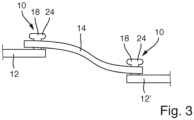
- Figure 3 shows a side view of several printed circuit boards 12, 14 connected to one another by contact connections 10 according to the invention.
- the first printed circuit board 12 is a rigid printed circuit board
- the second printed circuit board 14 is a flexible printed circuit board.
- a further rigid printed circuit board 12' is provided.
- the first printed circuit board 12 comprises, for example, a glass fiber mat impregnated with epoxy resin, which is also known by the material identifier FR4, as a non-conductive carrier material.
- the second printed circuit board 14 is, for example, a particularly thin printed circuit board based on polyimide films. According to the illustrated embodiment, the second printed circuit board 14 is provided for connecting the two rigid printed circuit boards 12, 12'.
- An LED printed circuit board comprises one or more LEDs, with multiple printed circuit boards being used, in particular, in lighting devices with multi-chamber reflectors and/or with multiple feed points.
Landscapes
- Engineering & Computer Science (AREA)
- Manufacturing & Machinery (AREA)
- Microelectronics & Electronic Packaging (AREA)
- Combinations Of Printed Boards (AREA)
- Coupling Device And Connection With Printed Circuit (AREA)
Description
- Die Erfindung betrifft eine elektrisch leitende Kontaktverbindung zwischen einer ersten und einer zweiten Leiterplatte gemäß dem Oberbegriff des Anspruchs 1.
- Ferner betrifft die Erfindung ein Verfahren zum Herstellen einer elektrisch leitenden Kontaktverbindung zwischen einer ersten Leiterplatte und einer zweiten Leiterplatte gemäß dem Oberbegriff des Anspruchs 3.
- Elektrisch leitende Kontaktverbindungen zwischen Bauteilen, beispielsweise Leiterplatten, sind aus dem Stand der Technik bekannt. Aus der
DE 41 32 995 A1 ist es beispielsweise bekannt Kontakte einer starren Leiterplatte mit Kontakten einer flexiblen Leiterplatte zu verlöten. Ferner ist es beispielsweise bekannt zwei Leiterplatten, insbesondere einer starre und eine flexible Leiterplatte, über sogenannte Steckverbinderleisten und Leiterplattenbuchsen, Stift- oder Buchsenleisten, die auf den Leiterplatten montiert sind, miteinander zu verbinden. Ferner sind aus derUS 3,980,367 A ,JP H08 213068 A EP 2 107 642 A2 Verbindungen mit den Merkmalen des Oberbegriffs des Anspruchs 1 bekannt, bei denen ein Verbindungselement zunächst gleichzeitig durch Öffnungen in zwei oder mehr Leiterplatten hindurchgeführt wird und anschließend durch Umformen des Verbindungselements eine Verbindung hergestellt wird. -
EP 0 664 576 A2 offenbart eine Verbindungselement, das zunächst durch Umformen mit einer ersten Leiterplatte und anschließend durch Einpressen mit einer weiteren Leiterplatte verbunden wird. - Aufgabe der vorliegenden Erfindung ist es eine gegenüber dem Stand der Technik kostengünstigere, mit einem geringeren Aufwand herstellbare elektrisch leitende Kontaktverbindung und ein Verfahren zum Herstellen der elektrisch leitenden Kontaktverbindung anzugeben.
- Erfindungsgemäß wird vorgeschlagen, dass die erste Leiterplatte im Bereich der Kontaktverbindung einen Anschlussstift umfasst und die zweite Leiterplatte im Bereich der Kontaktverbindung eine Durchstecköffnung umfasst, wobei der Anschlussstift der ersten Leiterplatte wenigstens teilweise aus einem elektrisch leitfähigen Material ausgebildet ist und durch die Durchstecköffnung der zweiten Leiterplatte hindurch gesteckt ist, wobei der Anschlussstift in einem durch die Durchstecköffnung der zweiten Leiterplatte über die zweite Leiterplatte herausragenden Abschnitt durch einen Umformvorgang, insbesondere einen Biegevorgang oder einen Nietvorgang, derart umgeformt ist, dass zwischen der ersten und der zweiten Leiterplatte eine formschlüssige Verbindung ausgebildet ist.
- Die erfindungsgemäße Kontaktverbindung ist, ohne einen weiteren Lötvorgang zu erfordern, herstellbar. Im Vergleich zu einer Steckverbindung erfordert die erfindungsgemäße Kontaktverbindung wenig Materialaufwand.
- Der Anschlussstift umfasst insbesondere eine zylindrische Form und ist wenigstens in einem durch die Durchstecköffnung der zweiten Leiterplatte, über die zweite Leiterplatte herausragenden, Abschnitt plastisch verformbar.
- Der Anschlussstift ist beispielsweise aus Metall und/oder einer Legierung und/oder teilweise aus Kunststoff in Kombination mit einem elektrisch leitfähigen Material hergestellt.
- Der Anschlussstift ist in dem durch die Durchstecköffnung der zweiten Leiterplatte, über die zweite Leiterplatte herausragenden, Abschnitt, unter Krafteinwirkung mittels einem geeigneten Werkzeug, derart umgeformt worden, dass der umgeformte Abschnitt die zweite Leiterplatte teilweise überragend gegen die erste Leiterplatte hält.
- Vorteilhafterweise umfasst eine Innenwandung der Durchstecköffnung der zweiten Leiterplatte ein elektrisch leitfähiges Material. Der, durch die Durchtrittsöffnung der zweiten Leiterplatte, hindurchgesteckte Anschlussstift der ersten Leiterplatte kontaktiert die Innenwandung zumindest teilweise, vorzugsweise vollumfänglich, so dass dadurch eine elektrisch leitende Verbindung ausgebildet ist.
- Der Anschlussstift ist mit der ersten Leiterplatte mittels eines Pin-in-Paste-Lötverfahrens, verbunden. Der Anschlussstift ist durch eine Öffnung, ein sogenanntes Bestückungsloch, in der ersten Leiterplatte geführt und mit der ersten Leiterplatte verlötet. Beispielsweise ist der Anschlussstift auf einer Rückseite der ersten Leiterplatte oder im Falle des Pin-in-Paste-Lötverfahrens in der Öffnung mit der ersten Leiterplatte verlötet. Beim Pin-in-Paste-Lötverfahren wird Lotpaste in die Öffnung gedruckt und anschließend der Anschlussstift hindurchgesteckt. Beim Aufschmelzen der Lotpaste zieht sich das flüssige Lot in die Öffnung zurück und bildet die Lötverbindung aus. Ebenfalls wäre es denkbar, dass der Anschlussstift in einem die erste Leiterplatte, auf der Rückseite der ersten Leiterplatte, überragenden Abschnitt einen vorgefertigten Setzkopf umfasst, so dass die Nietverbindung durch Umformen des über die zweite Leiterplatte herausragenden, Abschnitt geschlossen wird.
- Alternativ ist der Anschlussstift mit der ersten Leiterplatte mittels eines SMT-, Surface-Mounting-Technologie, Lötverfahrens, verbunden. Der Anschlussstift ist dann mittels lötfähiger Anschlussflächen direkt auf die erste Leiterplatte gelötet.
- Die erste Leiterplatte ist eine starre Leiterplatte und die zweite Leiterplatte ist eine flexible Leiterplatte. Die erste Leiterplatte umfasst beispielsweise als nichtleitendes Trägermaterial eine mit Epoxidharz getränkte Glasfasermatte, auch unter der Materialkennung FR4 bekannt. Die zweite Leiterplatte ist beispielsweise eine, insbesondere dünne, Leiterplatte auf Basis von Polyimid-Folien. Solche Leiterplatten können vorteilhafterweise platzsparend, insbesondere durch Falten in engsten Strukturen, beispielsweise in Beleuchtungseinrichtungen, und/oder zum Verbinden von zwei starren Leiterplatten, beispielsweise in Beleuchtungseinrichtungen, verwendet werden.
- Weitere bevorzugte Ausführungsformen beziehen sich auf ein Verfahren zum Herstellen einer elektrisch leitenden Kontaktverbindung zwischen einer ersten Leiterplatte und einer zweiten Leiterplatte, wobei die erste Leiterplatte im Bereich der Kontaktverbindung einen Anschlussstift umfasst und die zweite Leiterpatte im Bereich der Kontaktverbindung eine Durchstecköffnung umfasst, wobei der Anschlussstift der ersten Leiterplatte wenigstens teilweise aus einem elektrisch leitfähigen Material ausgebildet ist, dadurch gekennzeichnet, dass der Anschlussstift der ersten Leiterplatte durch die Durchstecköffnung der zweiten Leiterplatte hindurch gesteckt wird, und anschließend ein durch die Durchstecköffnung der zweiten Leiterplatte über die zweite Leiterplatte herausragender Abschnitt des Anschlussstifts in einem Umformvorgang, insbesondere einem Biegevorgang oder einem Nietvorgang, derart umgeformt wird, dass zwischen der ersten und der zweiten Leiterplatte eine formschlüssige Verbindung ausgebildet wird.
- Der Anschlussstift wird in dem Umformvorgang in dem durch die Durchstecköffnung der zweiten Leiterplatte, über die zweite Leiterplatte herausragenden, Abschnitt, unter Krafteinwirkung mittels einem geeigneten Werkzeug, derart umgeformt, dass der umgeformte Abschnitt anschließend die zweite Leiterplatte teilweise überragend gegen die erste Leiterplatte hält.
- Das Umformen umfasst beispielsweise ein sogenanntes Anstauchen des Anschlussstiftes und/oder das Vorformen eines Nietkopfs, insbesondere durch kreisende Schläge mit dem Kugelkopfhammer, und/oder das endgültige Formen des Nietkopfs, insbesondere mittels eines Nietkopfsetzers.
- Der Anschlussstift wird in einem vorhergehenden Schritt mit der ersten Leiterplatte mittels eines Pin-in-Paste Lötverfahrens, verbunden.
- Alternativ wird der Anschlussstift in einem vorhergehenden Schritt mit der ersten Leiterplattem mittels eines SMT-, Surface-Mounting-Technologie-, Lötverfahren, verbunden. Ausführungsbeispiele der Erfindung sind in den Zeichnungen dargestellt und werden in der nachfolgenden Beschreibung näher erläutert. Dabei bezeichnen gleiche Bezugszeichen in verschiedenen Figuren jeweils gleiche oder zumindest ihrer Funktion nach vergleichbare Elemente. Es zeigen, jeweils in schematischer Form:
- Fig. 1
- eine erfindungsgemäße elektrisch leitende Kontaktverbindung gemäß einer ersten bevorzugten Ausführungsform;
- Fig. 2
- eine erfindungsgemäße elektrisch leitende Kontaktverbindung gemäß einer weiteren bevorzugten Ausführungsform, und
- Fig. 3
- mit erfindungsgemäßen Kontaktverbindungen miteinander verbundene Leiterplatten.
-
Fig. 1 zeigt eine erfindungsgemäße elektrisch leitende Kontaktverbindung gemäß einer ersten bevorzugten Ausführungsform in einer Schnittansicht, die in ihrer Gesamtheit mit dem Bezugszeichen 10 bezeichnet ist. Die Kontaktverbindung 10 verbindet eine erste Leiterplatte 12 mit einer zweiten Leiterplatte 14. Die zweite Leiterplatte 14 umfasst eine Durchstecköffnung 16 und die erste Leiterpatte 12 umfasst einen Anschlussstift 18, der durch die Durchstecköffnung 16 der zweiten Leiterplatte 14 hindurch gesteckt ist. - Der Anschlussstift 18 ist wenigstens teilweise aus einem elektrisch leitfähigen Material ausgebildet. Gemäß der in
Figur 1 dargestellten Ausführungsform ist der Anschlussstift 18 auf einer Oberfläche 20 der ersten Leiterplatte 12 montiert. Erfindungsgemäß ist der Anschlussstift 18 mittels eines SMT-, Surface-Mounting-Technologie, Lötverfahrens, mit der Oberfläche 20 der ersten Leiterplatte 12 verbunden. - Eine Innenwandung 22 der Durchstecköffnung 16 der zweiten Leiterplatte 14 umfasst ein elektrisch leitfähiges Material. Der Anschlussstift 18 kontaktiert die Innenwandung 22 zumindest teilweise, vorzugsweise vollumfänglich, so dass dadurch eine elektrisch leitende Verbindung ausgebildet ist, zwischen der ersten Leiterplatte 12 und der zweiten Leiterplatte 14 ausgebildet ist.
- Der Anschlussstift 18 ist in einem durch die Durchstecköffnung 16 der zweiten Leiterplatte 14 über die zweite Leiterplatte 14 herausragenden Abschnitt 24 durch einen Umformvorgang, insbesondere einen Biegevorgang oder einen Nietvorgang, derart umgeformt, dass zwischen der ersten und der zweiten Leiterplatte 12, 14 eine formschlüssige Verbindung ausgebildet ist. Der umgeformte Abschnitt 24 hält die zweite Leiterplatte 14 teilweise überragend gegen die erste Leiterplatte 12.
- Das Umformen erfolgt unter Krafteinwirkung mittels einem geeigneten Werkzeug. Das Umformen umfasst beispielsweise ein sogenanntes Anstauchen des Anschlussstiftes 18 und/oder das Vorformen der Abschnitts 24 in Form eines Nietkopfs, insbesondere durch kreisende Schläge mit dem Kugelkopfhammer, und/oder das endgültige Formen des Abschnitts 24 in Form eines Nietkopfs, insbesondere mittels eines Nietkopfsetzers.
-
Figur 2 zeigt die Kontaktverbindung 10 gemäß einer weiteren Ausführungsform in einer Schnittansicht. Der Anschlussstift 18 der ersten Leiterplatte ist mit der ersten Leiterplatte 12 mittels Durchkontaktierung verbunden. - Die erste Leiterplatte 12 umfasst dazu eine Öffnung 26, ein sogenanntes Bestückungsloch. Der Anschlussstift 18 ist durch die Öffnung 26 der ersten Leiterplatte 12 durchgeführt und mit der ersten Leiterplatte 12 verlötet. Gemäß der Erfindung ist der Anschlussstift 18 mittels eines Pin-in-Paste-Lötverfahrens in der Öffnung 26 mit der ersten Leiterplatte 12 verlötet. Dazu wird zunächst eine Lotpaste in die Öffnung 26 gedruckt und anschließend der Anschlussstift 18 hindurchgesteckt. Beim Aufschmelzen der Lotpaste zieht sich das flüssige Lot in die Öffnung 26 zurück und bildet die Lötverbindung 28 aus. Gemäß einer nicht dargestellten Ausführungsform ist es auch denkbar, dass der Anschlussstift 18 auf einer Rückseite 30 der ersten Leiterplatte 12 verlötet ist.
- Ebenfalls wäre es denkbar, dass der Anschlussstift in einem die erste Leiterplatte 12 auf der Rückseite 30 überragenden Abschnitt einen vorgefertigten Setzkopf umfasst, so dass die Nietverbindung durch Umformen des über die zweite Leiterplatte 14 herausragenden Abschnitt 24 geschlossen wird.
-
Figur 3 zeigt mehrere mit erfindungsgemäßen Kontaktverbindungen 10 miteinander verbundene Leiterplatten 12, 14 in einer Ansicht von der Seite. Die erste Leiterplatte 12 eine starre Leiterplatte und die zweite Leiterplatte 14 ist eine flexible Leiterplatte. Ferner ist eine weitere, starre Leiterplatte 12' vorgesehen. Die erste Leiterplatte 12 umfasst beispielsweise als nichtleitendes Trägermaterial eine mit Epoxidharz getränkte Glasfasermatte, welches auch unter der Materialkennung FR4 bekannt ist. Die zweite Leiterplatte 14 ist beispielsweise eine, insbesondere dünne, Leiterplatte auf Basis von Polyimid-Folien. Gemäß der dargestellten Ausführungsform ist die zweite Leiterplatte 14 zum Verbinden der zwei starren Leiterplatten 12, 12', vorgesehen. Eine solche Verwendung ist beispielsweise in Beleuchtungseinrichtungen, insbesondere zum Verbinden von LED-Leiterplatten, denkbar. Eine LED-Leiterplatte umfasst dabei eine oder mehrere LEDs, wobei mehrere Leiterplatten insbesondere bei Beleuchtungseinrichtungen mit Mehrkammerreflektoren oder/oder mit mehreren Einspeisepunkten verwendet werden.
Claims (3)
- Elektrisch leitende Kontaktverbindung (10) zwischen einer ersten und einer zweiten Leiterplatte (12, 14), umfassend die erste und die zweite Leiterplatte und einen Anschlussstift (18), wobei die erste Leiterplatte (12) eine starre Leiterplatte und die zweite Leiterplatte (14) eine flexible Leiterplatte ist, wobei die erste Leiterplatte (12) im Bereich der Kontaktverbindung (10) den Anschlussstift (18) umfasst und die zweite Leiterpatte (14) im Bereich der Kontaktverbindung (10) eine Durchstecköffnung (16) umfasst, wobei der Anschlussstift (18) der ersten Leiterplatte (12) wenigstens teilweise aus einem elektrisch leitfähigen Material ausgebildet ist und durch die Durchstecköffnung (16) der zweiten Leiterplatte (14) hindurch gesteckt ist, wobei der Anschlussstift (18) in einem durch die Durchstecköffnung (16) der zweiten Leiterplatte (14) über die zweite Leiterplatte (14) herausragenden Abschnitt (24) durch einen Umformvorgang, insbesondere einen Biegevorgang oder einen Nietvorgang, derart umgeformt ist, dass zwischen der ersten und der zweiten Leiterplatte (12, 14) eine formschlüssige Verbindung ausgebildet ist, dadurch gekennzeichnet, dass der Anschlussstift (18) mit der ersten Leiterplatte (12) mittels eines Pin-in-Paste-Lötverfahrens, oder mittels eines SMT-, Surface-Mounting-Technologie, Lötverfahrens, verbunden ist.
- Kontaktverbindung (10) nach Anspruch 1, dadurch gekennzeichnet, dass eine Innenwandung (22) der Durchstecköffnung (16) der zweiten Leiterplatte (14) ein elektrisch leitfähiges Material umfasst.
- Verfahren zum Herstellen einer elektrisch leitenden Kontaktverbindung (10) zwischen einer ersten Leiterplatte (12) und einer zweiten Leiterplatte (14) umfassend die erste und die zweite Leiterplatte (12, 14) und einen Anschlussstift (18), wobei die erste Leiterplatte (12) eine starre Leiterplatte und die zweite Leiterplatte (14) eine flexible Leiterplatte ist, wobei die erste Leiterplatte (12) im Bereich der Kontaktverbindung (10) den Anschlussstift (18) umfasst und die zweite Leiterplatte (14) im Bereich der Kontaktverbindung (10) eine Durchstecköffnung (16) umfasst, wobei der Anschlussstift (18) der ersten Leiterplatte (12) wenigstens teilweise aus einem elektrisch leitfähigen Material ausgebildet ist, wobei der Anschlussstift (18) der ersten Leiterplatte (12) durch die Durchstecköffnung (16) der zweiten Leiterplatte (14) hindurch gesteckt wird, und anschließend ein durch die Durchstecköffnung (16) der zweiten Leiterplatte (14) über die zweite Leiterplatte (14) herausragender Abschnitt (24) des Anschlussstifts (18) in einem Umformvorgang, insbesondere einem Biegevorgang oder einem Nietvorgang, derart umgeformt wird, dass zwischen der ersten und der zweiten Leiterplatte (12, 14) eine formschlüssige Verbindung ausgebildet wird, dadurch gekennzeichnet, dass der Anschlussstift (18) in einem vorhergehenden Schritt mit der ersten Leiterplatte (12) mittels eines Pin-in-Paste Lötverfahrens, oder dass der Anschlussstift (18) in einem vorhergehenden Schritt mit der ersten Leiterplatte (12) mittels eines SMT-, Surface-Mounting-Technologie-, Lötverfahrens, verbunden wird.
Applications Claiming Priority (1)
| Application Number | Priority Date | Filing Date | Title |
|---|---|---|---|
| DE102019129719.2A DE102019129719A1 (de) | 2019-11-05 | 2019-11-05 | Elektrisch leitende Verbindung von Leiterplatten |
Publications (2)
| Publication Number | Publication Date |
|---|---|
| EP3819988A1 EP3819988A1 (de) | 2021-05-12 |
| EP3819988B1 true EP3819988B1 (de) | 2025-04-23 |
Family
ID=72840289
Family Applications (1)
| Application Number | Title | Priority Date | Filing Date |
|---|---|---|---|
| EP20201049.2A Active EP3819988B1 (de) | 2019-11-05 | 2020-10-09 | Elektrisch leitende verbindung von leiterplatten |
Country Status (3)
| Country | Link |
|---|---|
| EP (1) | EP3819988B1 (de) |
| CN (1) | CN112787119B (de) |
| DE (1) | DE102019129719A1 (de) |
Families Citing this family (2)
| Publication number | Priority date | Publication date | Assignee | Title |
|---|---|---|---|---|
| CN115066092B (zh) * | 2021-10-09 | 2023-03-24 | 荣耀终端有限公司 | 电路板组件、制造方法及电子设备 |
| DE102022120904A1 (de) | 2022-08-18 | 2024-02-29 | Bayerische Motoren Werke Aktiengesellschaft | Elektrische Kontaktverbindung, elektrischer Mehrfachanschluss für ein Fahrzeug sowie ein Fahrzeug |
Citations (3)
| Publication number | Priority date | Publication date | Assignee | Title |
|---|---|---|---|---|
| DE2624330A1 (de) * | 1976-05-31 | 1977-12-15 | Siemens Ag | Anordnung zur durchkontaktierung zweier auf unterschiedlichen seiten eines schaltungstraegers liegender leiterbahnen |
| DE60209408T2 (de) * | 2001-08-13 | 2006-09-21 | Autosplice, Inc., San Diego | Lötkugelkontakt und Leiterplatte mit solchem Kontakt |
| DE202007002940U1 (de) * | 2007-02-28 | 2007-04-26 | Patent-Treuhand-Gesellschaft für elektrische Glühlampen mbH | Elektronisches Bauteil und elektrischer Schaltungsträger |
Family Cites Families (15)
| Publication number | Priority date | Publication date | Assignee | Title |
|---|---|---|---|---|
| US3980367A (en) * | 1975-03-19 | 1976-09-14 | Sealectro Corporation | Electrical connector for joining conductors attached to printed circuit boards |
| GB2031763B (en) * | 1978-10-16 | 1982-07-28 | Ultra Electronic Controls Ltd | Connections between a flexible circuit board and a rigid member |
| DE4132995A1 (de) * | 1991-10-04 | 1993-04-08 | Bodenseewerk Geraetetech | Verfahren zur herstellung elektrisch leitender verbindungen an leiterplatten |
| US5548486A (en) * | 1994-01-21 | 1996-08-20 | International Business Machines Corporation | Pinned module |
| JPH08213068A (ja) * | 1995-02-09 | 1996-08-20 | Fujikura Ltd | フレキシブルプリント基板とテープ電線との接続方法 |
| DE29706016U1 (de) * | 1997-04-04 | 1998-08-06 | TELBUS Gesellschaft für elektronische Kommunikations-Systeme mbH, 85391 Allershausen | Elektronisches Gerät, insbesondere Chipkarte mit Nietverbindung |
| DE102004058691A1 (de) * | 2004-12-06 | 2006-06-14 | Robert Bosch Gmbh | Anordung einer elektrischen Verbindung und Verfahren zur Herstellung derselben |
| CN101238244B (zh) * | 2005-01-24 | 2011-03-30 | 株式会社昭和 | 采用阳极电解氧化处理的结晶性氧化钛被膜的制造方法 |
| US7448923B2 (en) * | 2006-09-14 | 2008-11-11 | Harshad K Uka | Connection for flex circuit and rigid circuit board |
| DE102007008109B4 (de) * | 2007-02-19 | 2022-10-27 | Osram Gmbh | Trägerplattenanordnung |
| EP2107642A3 (de) * | 2008-04-04 | 2011-04-20 | Amphenol-Tuchel Electronics GmbH | Verbindungsanordnung und Verfahren zur Kontaktierung von leitfähigen textilen Halbzeugen |
| JP5142386B2 (ja) * | 2008-08-06 | 2013-02-13 | 日本航空電子工業株式会社 | コネクタ |
| DE102011084326A1 (de) * | 2011-10-12 | 2013-04-18 | Osram Opto Semiconductors Gmbh | Flexible Leiterplatte zur elektrischen Kontaktierung und mechanischen Befestigung einer Lampe in einer Leuchte |
| DE102016002821A1 (de) * | 2016-03-05 | 2017-09-07 | Wabco Gmbh | Schaltkreis einer elektronischen Steuereinheit |
| DE102016218788A1 (de) * | 2016-09-29 | 2018-03-29 | Zf Friedrichshafen Ag | Leiterplattenverbindung |
-
2019
- 2019-11-05 DE DE102019129719.2A patent/DE102019129719A1/de active Pending
-
2020
- 2020-10-09 EP EP20201049.2A patent/EP3819988B1/de active Active
- 2020-11-04 CN CN202011214076.6A patent/CN112787119B/zh active Active
Patent Citations (3)
| Publication number | Priority date | Publication date | Assignee | Title |
|---|---|---|---|---|
| DE2624330A1 (de) * | 1976-05-31 | 1977-12-15 | Siemens Ag | Anordnung zur durchkontaktierung zweier auf unterschiedlichen seiten eines schaltungstraegers liegender leiterbahnen |
| DE60209408T2 (de) * | 2001-08-13 | 2006-09-21 | Autosplice, Inc., San Diego | Lötkugelkontakt und Leiterplatte mit solchem Kontakt |
| DE202007002940U1 (de) * | 2007-02-28 | 2007-04-26 | Patent-Treuhand-Gesellschaft für elektrische Glühlampen mbH | Elektronisches Bauteil und elektrischer Schaltungsträger |
Also Published As
| Publication number | Publication date |
|---|---|
| DE102019129719A1 (de) | 2021-05-06 |
| EP3819988A1 (de) | 2021-05-12 |
| CN112787119A (zh) | 2021-05-11 |
| CN112787119B (zh) | 2026-02-13 |
Similar Documents
| Publication | Publication Date | Title |
|---|---|---|
| DE69113679T2 (de) | Verfahren und Bauteil zum Montieren von Bauelementen auf einer Leiterplatte. | |
| EP0941020A2 (de) | Leiterplatte mit SMD-Bauelementen | |
| DE102009058825A1 (de) | Kontaktvorrichtung zum Befestigen an einer Leiterplatte, Verfahren zum Befestigen einer Kontaktvorrichtung an einer Leiterplatte und Leiterplatte | |
| DE102017105134B4 (de) | Montagehilfe zum Montieren von elektrischen Bauteilen auf einer Leiterplatte und Verfahren zum Montieren von elektrischen Bauteilen auf einer Leiterplatte | |
| EP3819989B1 (de) | Elektrisch leitende verbindung von leiterplatten | |
| WO2015165946A1 (de) | Elektrische verbindungsanordnung für die elektrische verbindung von leiterplatten untereinander mittels lötfreier einpresskontaktierung | |
| DE102017125505A1 (de) | Steckerbuchse für Leiterplatinen | |
| EP3819988A1 (de) | Elektrisch leitende verbindung von leiterplatten | |
| DE202010013758U1 (de) | Einlötkontaktanordnung | |
| DE102008017828A1 (de) | Verbindungsverfahren und verbundene Einheit | |
| DE102007005877B4 (de) | Verbindungssystem für Leiterplatten | |
| DE102004049575B4 (de) | Elektrisches Anschlusselement und Verfahren zum Anschließen eines Leiterkabels | |
| DE102007005824B4 (de) | Verbindungselement für eine doppelseitige Leiterplatte | |
| EP2109186B1 (de) | Verfahren zur Herstellung einer elektrischen Verbindung zwischen einer Stromschiene und einer Leiterplatte | |
| WO2016000909A1 (de) | Leiterplattenverbindungselement | |
| DE102005058089A1 (de) | Verfahren zum Einsetzen eines Steckteils in eine durchgängige Anschlußbohrung und Herstellen einer hochfesten elektrisch leitenden Verbindung | |
| DE102012112546A1 (de) | Verfahren zur Herstellung von mischbestückten Leiterplatten | |
| DE10254161B4 (de) | Gasgenerator-Erdungsvorrichtung und Verfahren zu ihrer Herstellung | |
| EP4205239A1 (de) | Elektrische kontaktanordnung sowie leiterplattenanordnung und verfahren zu deren herstellung | |
| EP1645013B1 (de) | Bauteil für eine leiterplatte | |
| EP1659837B1 (de) | Kontaktierung eines Bauelementes auf einem Stanzgitter | |
| DE10023967C2 (de) | Kontaktelement für geschirmte Kabel oder Leitungen | |
| DE102022203680B3 (de) | Verbindungsvorrichtung und Verfahren zum Herstellen einer Verbindungsvorrichtung | |
| EP2187719A1 (de) | Verbindungsträger für Lötstifte | |
| DE102004031133B3 (de) | Flachsteckkontakt, insbesondere für Kfz-Motor- oder Getriebesteuerungen und Verfahren zu seiner Herstellung |
Legal Events
| Date | Code | Title | Description |
|---|---|---|---|
| PUAI | Public reference made under article 153(3) epc to a published international application that has entered the european phase |
Free format text: ORIGINAL CODE: 0009012 |
|
| STAA | Information on the status of an ep patent application or granted ep patent |
Free format text: STATUS: THE APPLICATION HAS BEEN PUBLISHED |
|
| AK | Designated contracting states |
Kind code of ref document: A1 Designated state(s): AL AT BE BG CH CY CZ DE DK EE ES FI FR GB GR HR HU IE IS IT LI LT LU LV MC MK MT NL NO PL PT RO RS SE SI SK SM TR |
|
| STAA | Information on the status of an ep patent application or granted ep patent |
Free format text: STATUS: REQUEST FOR EXAMINATION WAS MADE |
|
| 17P | Request for examination filed |
Effective date: 20211102 |
|
| RBV | Designated contracting states (corrected) |
Designated state(s): AL AT BE BG CH CY CZ DE DK EE ES FI FR GB GR HR HU IE IS IT LI LT LU LV MC MK MT NL NO PL PT RO RS SE SI SK SM TR |
|
| STAA | Information on the status of an ep patent application or granted ep patent |
Free format text: STATUS: EXAMINATION IS IN PROGRESS |
|
| 17Q | First examination report despatched |
Effective date: 20230217 |
|
| GRAP | Despatch of communication of intention to grant a patent |
Free format text: ORIGINAL CODE: EPIDOSNIGR1 |
|
| STAA | Information on the status of an ep patent application or granted ep patent |
Free format text: STATUS: GRANT OF PATENT IS INTENDED |
|
| INTG | Intention to grant announced |
Effective date: 20241210 |
|
| GRAS | Grant fee paid |
Free format text: ORIGINAL CODE: EPIDOSNIGR3 |
|
| GRAA | (expected) grant |
Free format text: ORIGINAL CODE: 0009210 |
|
| STAA | Information on the status of an ep patent application or granted ep patent |
Free format text: STATUS: THE PATENT HAS BEEN GRANTED |
|
| RAP3 | Party data changed (applicant data changed or rights of an application transferred) |
Owner name: MARELLI GERMANY GMBH |
|
| P01 | Opt-out of the competence of the unified patent court (upc) registered |
Free format text: CASE NUMBER: APP_10730/2025 Effective date: 20250304 |
|
| AK | Designated contracting states |
Kind code of ref document: B1 Designated state(s): AL AT BE BG CH CY CZ DE DK EE ES FI FR GB GR HR HU IE IS IT LI LT LU LV MC MK MT NL NO PL PT RO RS SE SI SK SM TR |
|
| REG | Reference to a national code |
Ref country code: GB Ref legal event code: FG4D Free format text: NOT ENGLISH |
|
| REG | Reference to a national code |
Ref country code: CH Ref legal event code: EP |
|
| REG | Reference to a national code |
Ref country code: DE Ref legal event code: R096 Ref document number: 502020010880 Country of ref document: DE |
|
| REG | Reference to a national code |
Ref country code: IE Ref legal event code: FG4D Free format text: LANGUAGE OF EP DOCUMENT: GERMAN |
|
| REG | Reference to a national code |
Ref country code: NL Ref legal event code: MP Effective date: 20250423 |
|
| PG25 | Lapsed in a contracting state [announced via postgrant information from national office to epo] |
Ref country code: NL Free format text: LAPSE BECAUSE OF FAILURE TO SUBMIT A TRANSLATION OF THE DESCRIPTION OR TO PAY THE FEE WITHIN THE PRESCRIBED TIME-LIMIT Effective date: 20250423 |
|
| PG25 | Lapsed in a contracting state [announced via postgrant information from national office to epo] |
Ref country code: PT Free format text: LAPSE BECAUSE OF FAILURE TO SUBMIT A TRANSLATION OF THE DESCRIPTION OR TO PAY THE FEE WITHIN THE PRESCRIBED TIME-LIMIT Effective date: 20250825 Ref country code: ES Free format text: LAPSE BECAUSE OF FAILURE TO SUBMIT A TRANSLATION OF THE DESCRIPTION OR TO PAY THE FEE WITHIN THE PRESCRIBED TIME-LIMIT Effective date: 20250423 Ref country code: FI Free format text: LAPSE BECAUSE OF FAILURE TO SUBMIT A TRANSLATION OF THE DESCRIPTION OR TO PAY THE FEE WITHIN THE PRESCRIBED TIME-LIMIT Effective date: 20250423 |
|
| REG | Reference to a national code |
Ref country code: LT Ref legal event code: MG9D |
|
| PG25 | Lapsed in a contracting state [announced via postgrant information from national office to epo] |
Ref country code: GR Free format text: LAPSE BECAUSE OF FAILURE TO SUBMIT A TRANSLATION OF THE DESCRIPTION OR TO PAY THE FEE WITHIN THE PRESCRIBED TIME-LIMIT Effective date: 20250724 Ref country code: NO Free format text: LAPSE BECAUSE OF FAILURE TO SUBMIT A TRANSLATION OF THE DESCRIPTION OR TO PAY THE FEE WITHIN THE PRESCRIBED TIME-LIMIT Effective date: 20250723 |
|
| PG25 | Lapsed in a contracting state [announced via postgrant information from national office to epo] |
Ref country code: PL Free format text: LAPSE BECAUSE OF FAILURE TO SUBMIT A TRANSLATION OF THE DESCRIPTION OR TO PAY THE FEE WITHIN THE PRESCRIBED TIME-LIMIT Effective date: 20250423 |
|
| PG25 | Lapsed in a contracting state [announced via postgrant information from national office to epo] |
Ref country code: BG Free format text: LAPSE BECAUSE OF FAILURE TO SUBMIT A TRANSLATION OF THE DESCRIPTION OR TO PAY THE FEE WITHIN THE PRESCRIBED TIME-LIMIT Effective date: 20250423 |
|
| PG25 | Lapsed in a contracting state [announced via postgrant information from national office to epo] |
Ref country code: HR Free format text: LAPSE BECAUSE OF FAILURE TO SUBMIT A TRANSLATION OF THE DESCRIPTION OR TO PAY THE FEE WITHIN THE PRESCRIBED TIME-LIMIT Effective date: 20250423 |
|
| PG25 | Lapsed in a contracting state [announced via postgrant information from national office to epo] |
Ref country code: RS Free format text: LAPSE BECAUSE OF FAILURE TO SUBMIT A TRANSLATION OF THE DESCRIPTION OR TO PAY THE FEE WITHIN THE PRESCRIBED TIME-LIMIT Effective date: 20250723 |
|
| PG25 | Lapsed in a contracting state [announced via postgrant information from national office to epo] |
Ref country code: IS Free format text: LAPSE BECAUSE OF FAILURE TO SUBMIT A TRANSLATION OF THE DESCRIPTION OR TO PAY THE FEE WITHIN THE PRESCRIBED TIME-LIMIT Effective date: 20250823 |
|
| PG25 | Lapsed in a contracting state [announced via postgrant information from national office to epo] |
Ref country code: LV Free format text: LAPSE BECAUSE OF FAILURE TO SUBMIT A TRANSLATION OF THE DESCRIPTION OR TO PAY THE FEE WITHIN THE PRESCRIBED TIME-LIMIT Effective date: 20250423 |
|
| PGFP | Annual fee paid to national office [announced via postgrant information from national office to epo] |
Ref country code: DE Payment date: 20250923 Year of fee payment: 6 |
|
| PG25 | Lapsed in a contracting state [announced via postgrant information from national office to epo] |
Ref country code: DK Free format text: LAPSE BECAUSE OF FAILURE TO SUBMIT A TRANSLATION OF THE DESCRIPTION OR TO PAY THE FEE WITHIN THE PRESCRIBED TIME-LIMIT Effective date: 20250423 Ref country code: SM Free format text: LAPSE BECAUSE OF FAILURE TO SUBMIT A TRANSLATION OF THE DESCRIPTION OR TO PAY THE FEE WITHIN THE PRESCRIBED TIME-LIMIT Effective date: 20250423 |
|
| PG25 | Lapsed in a contracting state [announced via postgrant information from national office to epo] |
Ref country code: CZ Free format text: LAPSE BECAUSE OF FAILURE TO SUBMIT A TRANSLATION OF THE DESCRIPTION OR TO PAY THE FEE WITHIN THE PRESCRIBED TIME-LIMIT Effective date: 20250423 |
|
| PG25 | Lapsed in a contracting state [announced via postgrant information from national office to epo] |
Ref country code: EE Free format text: LAPSE BECAUSE OF FAILURE TO SUBMIT A TRANSLATION OF THE DESCRIPTION OR TO PAY THE FEE WITHIN THE PRESCRIBED TIME-LIMIT Effective date: 20250423 |
|
| REG | Reference to a national code |
Ref country code: DE Ref legal event code: R097 Ref document number: 502020010880 Country of ref document: DE |
|
| PG25 | Lapsed in a contracting state [announced via postgrant information from national office to epo] |
Ref country code: RO Free format text: LAPSE BECAUSE OF FAILURE TO SUBMIT A TRANSLATION OF THE DESCRIPTION OR TO PAY THE FEE WITHIN THE PRESCRIBED TIME-LIMIT Effective date: 20250423 Ref country code: SK Free format text: LAPSE BECAUSE OF FAILURE TO SUBMIT A TRANSLATION OF THE DESCRIPTION OR TO PAY THE FEE WITHIN THE PRESCRIBED TIME-LIMIT Effective date: 20250423 |
|
| PG25 | Lapsed in a contracting state [announced via postgrant information from national office to epo] |
Ref country code: IT Free format text: LAPSE BECAUSE OF FAILURE TO SUBMIT A TRANSLATION OF THE DESCRIPTION OR TO PAY THE FEE WITHIN THE PRESCRIBED TIME-LIMIT Effective date: 20250423 |
|
| PLBE | No opposition filed within time limit |
Free format text: ORIGINAL CODE: 0009261 |
|
| STAA | Information on the status of an ep patent application or granted ep patent |
Free format text: STATUS: NO OPPOSITION FILED WITHIN TIME LIMIT |
|
| REG | Reference to a national code |
Ref country code: CH Ref legal event code: L10 Free format text: ST27 STATUS EVENT CODE: U-0-0-L10-L00 (AS PROVIDED BY THE NATIONAL OFFICE) Effective date: 20260304 |
|
| 26N | No opposition filed |
Effective date: 20260126 |