EP3799111B1 - Inspection device and temperature control method - Google Patents
Inspection device and temperature control method Download PDFInfo
- Publication number
- EP3799111B1 EP3799111B1 EP19807713.3A EP19807713A EP3799111B1 EP 3799111 B1 EP3799111 B1 EP 3799111B1 EP 19807713 A EP19807713 A EP 19807713A EP 3799111 B1 EP3799111 B1 EP 3799111B1
- Authority
- EP
- European Patent Office
- Prior art keywords
- electronic device
- inspection
- temperature
- refrigerant
- placement table
- Prior art date
- Legal status (The legal status is an assumption and is not a legal conclusion. Google has not performed a legal analysis and makes no representation as to the accuracy of the status listed.)
- Active
Links
- 238000007689 inspection Methods 0.000 title claims description 189
- 238000000034 method Methods 0.000 title claims description 29
- 239000003507 refrigerant Substances 0.000 claims description 82
- 239000000758 substrate Substances 0.000 claims description 71
- 238000010521 absorption reaction Methods 0.000 claims description 42
- 230000007704 transition Effects 0.000 claims description 35
- 238000010438 heat treatment Methods 0.000 claims description 33
- 230000007246 mechanism Effects 0.000 claims description 27
- 239000000523 sample Substances 0.000 description 18
- 238000012360 testing method Methods 0.000 description 15
- 238000005259 measurement Methods 0.000 description 10
- 230000001276 controlling effect Effects 0.000 description 9
- 230000001105 regulatory effect Effects 0.000 description 9
- 230000004308 accommodation Effects 0.000 description 8
- 238000001816 cooling Methods 0.000 description 7
- 230000008569 process Effects 0.000 description 6
- 230000001965 increasing effect Effects 0.000 description 5
- 239000004065 semiconductor Substances 0.000 description 5
- XLYOFNOQVPJJNP-UHFFFAOYSA-N water Substances O XLYOFNOQVPJJNP-UHFFFAOYSA-N 0.000 description 5
- 230000008859 change Effects 0.000 description 4
- 238000004806 packaging method and process Methods 0.000 description 4
- 238000012545 processing Methods 0.000 description 4
- NBVXSUQYWXRMNV-UHFFFAOYSA-N fluoromethane Chemical compound FC NBVXSUQYWXRMNV-UHFFFAOYSA-N 0.000 description 3
- 238000004519 manufacturing process Methods 0.000 description 3
- 230000007547 defect Effects 0.000 description 2
- 238000010586 diagram Methods 0.000 description 2
- 230000003028 elevating effect Effects 0.000 description 2
- 239000000463 material Substances 0.000 description 2
- 238000012546 transfer Methods 0.000 description 2
- 239000004925 Acrylic resin Substances 0.000 description 1
- 229920000178 Acrylic resin Polymers 0.000 description 1
- XUIMIQQOPSSXEZ-UHFFFAOYSA-N Silicon Chemical compound [Si] XUIMIQQOPSSXEZ-UHFFFAOYSA-N 0.000 description 1
- 230000002159 abnormal effect Effects 0.000 description 1
- 238000000137 annealing Methods 0.000 description 1
- 230000008901 benefit Effects 0.000 description 1
- 238000009529 body temperature measurement Methods 0.000 description 1
- 239000002826 coolant Substances 0.000 description 1
- 238000012937 correction Methods 0.000 description 1
- 230000003247 decreasing effect Effects 0.000 description 1
- 230000002950 deficient Effects 0.000 description 1
- 230000001419 dependent effect Effects 0.000 description 1
- 238000007599 discharging Methods 0.000 description 1
- 230000000694 effects Effects 0.000 description 1
- 238000005530 etching Methods 0.000 description 1
- 230000020169 heat generation Effects 0.000 description 1
- 230000010354 integration Effects 0.000 description 1
- 239000007788 liquid Substances 0.000 description 1
- 239000004973 liquid crystal related substance Substances 0.000 description 1
- 230000007257 malfunction Effects 0.000 description 1
- 229920003229 poly(methyl methacrylate) Polymers 0.000 description 1
- 239000004417 polycarbonate Substances 0.000 description 1
- 229920000515 polycarbonate Polymers 0.000 description 1
- 239000004926 polymethyl methacrylate Substances 0.000 description 1
- 239000004800 polyvinyl chloride Substances 0.000 description 1
- 229920000915 polyvinyl chloride Polymers 0.000 description 1
- 239000010453 quartz Substances 0.000 description 1
- 230000009467 reduction Effects 0.000 description 1
- 230000004044 response Effects 0.000 description 1
- 230000004043 responsiveness Effects 0.000 description 1
- 229910052710 silicon Inorganic materials 0.000 description 1
- 239000010703 silicon Substances 0.000 description 1
- VYPSYNLAJGMNEJ-UHFFFAOYSA-N silicon dioxide Inorganic materials O=[Si]=O VYPSYNLAJGMNEJ-UHFFFAOYSA-N 0.000 description 1
- 230000001131 transforming effect Effects 0.000 description 1
Images


Classifications
-
- G—PHYSICS
- G01—MEASURING; TESTING
- G01R—MEASURING ELECTRIC VARIABLES; MEASURING MAGNETIC VARIABLES
- G01R31/00—Arrangements for testing electric properties; Arrangements for locating electric faults; Arrangements for electrical testing characterised by what is being tested not provided for elsewhere
- G01R31/28—Testing of electronic circuits, e.g. by signal tracer
- G01R31/2851—Testing of integrated circuits [IC]
- G01R31/2855—Environmental, reliability or burn-in testing
- G01R31/2872—Environmental, reliability or burn-in testing related to electrical or environmental aspects, e.g. temperature, humidity, vibration, nuclear radiation
- G01R31/2874—Environmental, reliability or burn-in testing related to electrical or environmental aspects, e.g. temperature, humidity, vibration, nuclear radiation related to temperature
-
- G—PHYSICS
- G01—MEASURING; TESTING
- G01R—MEASURING ELECTRIC VARIABLES; MEASURING MAGNETIC VARIABLES
- G01R31/00—Arrangements for testing electric properties; Arrangements for locating electric faults; Arrangements for electrical testing characterised by what is being tested not provided for elsewhere
- G01R31/28—Testing of electronic circuits, e.g. by signal tracer
- G01R31/2851—Testing of integrated circuits [IC]
- G01R31/2855—Environmental, reliability or burn-in testing
- G01R31/286—External aspects, e.g. related to chambers, contacting devices or handlers
- G01R31/2862—Chambers or ovens; Tanks
-
- G—PHYSICS
- G01—MEASURING; TESTING
- G01R—MEASURING ELECTRIC VARIABLES; MEASURING MAGNETIC VARIABLES
- G01R31/00—Arrangements for testing electric properties; Arrangements for locating electric faults; Arrangements for electrical testing characterised by what is being tested not provided for elsewhere
- G01R31/28—Testing of electronic circuits, e.g. by signal tracer
- G01R31/2851—Testing of integrated circuits [IC]
- G01R31/2855—Environmental, reliability or burn-in testing
- G01R31/286—External aspects, e.g. related to chambers, contacting devices or handlers
- G01R31/2868—Complete testing stations; systems; procedures; software aspects
-
- G—PHYSICS
- G01—MEASURING; TESTING
- G01R—MEASURING ELECTRIC VARIABLES; MEASURING MAGNETIC VARIABLES
- G01R31/00—Arrangements for testing electric properties; Arrangements for locating electric faults; Arrangements for electrical testing characterised by what is being tested not provided for elsewhere
- G01R31/28—Testing of electronic circuits, e.g. by signal tracer
- G01R31/2851—Testing of integrated circuits [IC]
- G01R31/2855—Environmental, reliability or burn-in testing
- G01R31/2872—Environmental, reliability or burn-in testing related to electrical or environmental aspects, e.g. temperature, humidity, vibration, nuclear radiation
- G01R31/2879—Environmental, reliability or burn-in testing related to electrical or environmental aspects, e.g. temperature, humidity, vibration, nuclear radiation related to electrical aspects, e.g. to voltage or current supply or stimuli or to electrical loads
Definitions
- the present disclosure relates to an inspection apparatus and a temperature control method.
- Japanese laid-open publication No. 10-135315 discloses an inspection apparatus that performs electrical inspection of a semiconductor wafer on which an IC chip is formed under various temperature conditions in consideration of climatic conditions in which the IC chip is used.
- the inspection apparatus disclosed in Japanese laid-open publication No. 10-135315 includes a placement table on which the semiconductor wafer is placed, and a heater that heats the placement table. A gas flow path to which low-temperature air that cools the placement table is supplied is formed in the placement table.
- the device for regulating a temperature of a substrate within a chamber of a substrate processing apparatus includes a mounting stand, a substrate elevating mechanism, a first temperature regulating unit, a second temperature regulating unit, and a light transmitting window.
- the mounting stand is configured to mount the substrate thereon and includes a temperature regulating medium flow path formed therein.
- the substrate elevating mechanism is configured to move the substrate up and down between a first position and a second position.
- the first temperature regulating unit is configured to supply a temperature regulating medium to the flow path and configured to regulate the temperature of the substrate to a first temperature in the first position.
- the second temperature regulating unit is installed below the mounting stand and configured to regulate the substrate to a second temperature by emitting light toward the substrate in the second position and heating the substrate.
- the light transmitting window is configured to transmit the light emitted from the second temperature regulating unit.
- the apparatus includes a processing chamber for accommodating a wafer, heating sources including LEDs and facing the surface of the wafer to irradiate light on the wafer, light-transmitting members arranged in alignment with the heating sources to transmit the light emitted from the LEDs, cooling members supporting the light-transmitting members at opposite side to the processing chamber to make direct contact with the heating sources and made of a material of high thermal conductivity, and a cooling mechanism for cooling the cooling members with a coolant.
- the technique according to the present disclosure provides some embodiments of an inspection apparatus for an electronic device, and a temperature control method in the inspection apparatus, which are capable of suppressing an increase in cost of the electronic device.
- An aspect of the present disclosure is an inspecting apparatus comprising the combination of features of independent claim 1.
- Another aspect of the present disclosure is a temperature control method using an inspecting apparatus, the method comprising the combination of features of independent claim 3. Preferred embodiments are defined in dependent claims.
- an inspection apparatus for an electronic device and a temperature control method in the inspection apparatus, which are capable of suppressing an increase in cost of the electronic device.
- the inspection apparatus disclosed in Japanese laid-open publication No. 10-135315 includes a placement table on which a semiconductor wafer is mounted, and a heater that heats the placement table, and a gas flow path to which low-temperature air that cools the placement table is supplied is formed in the placement table.
- a voltage to be applied to the electronic device during inspection to be smaller than a relatively high mounting voltage to be applied in the mounting environment, it is possible to avoid the application of a thermal load to other adjacent electronic devices.
- a defect that occurs at the time of applying the mounting voltage before packaging of the electronic device resulting in a problem that the yield after the packaging is reduced and the cost is increased.
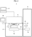
- FIGS. 1 and 2 are a perspective view and a front view, respectively, illustrating an outline of the configuration of the inspection apparatus 1 according to the present embodiment.
- FIG. 2 in order to show elements included in an accommodation chamber and a loader, which will be described later, of the inspection apparatus 1 of FIG. 1 , a portion thereof is shown in cross section.
- the inspection apparatus 1 inspects the electric characteristics of each of a plurality of electronic devices (see reference numeral D in FIG. 3 to be described later) formed on a substrate W. As illustrated in FIGS. 1 and 2 , the inspection apparatus 1 includes an accommodation chamber 2 for storing the wafer at the time of inspection, a loader 3 disposed adjacent to the accommodation chamber 2, and a tester 4 disposed to cover an upper portion of the accommodation chamber.
- the accommodation chamber 2 is a housing having an internal hollow, and has a stage 10 on which the substrate W to be inspected is placed.
- the stage 10 holds the substrate W by suction so that the position of the substrate W with respect to the stage 10 is not deviated.
- the stage 10 is configured to be movable in the horizontal direction and the vertical direction. With this configuration, the relative position between a probe card 11 to be described later and the substrate W is adjusted so that an electrode on the surface of the substrate W can be brought into contact with probes 11a of the probe card 11.
- the probe card 11 is disposed above the stage 10 inside the accommodation chamber 2 so as to face the stage 10.
- the probe card 11 has the probes 11a as contact terminals that are in electrical contact with electrodes or the like of electronic devices installed on the substrate W.
- the probe card 11 is connected to the tester 4 via an interface 12.
- each probe 11a contacts the electrode of each of the electronic devices on the substrate W, each probe 11a supplies electric power from the tester 4 to the electronic device via the interface 12, or transmits a signal from the electronic device to the tester 4 via the interface 12.
- the loader 3 takes out the substrate W accommodated in an FOUP (not shown), which is a transfer container, and transfers the same to the stage 10 inside the accommodation chamber 2. In addition, the loader 3 receives, from the stage 10, the substrate W for which the electrical characteristics of the electronic device D have been inspected, and stores the same in the FOUP.
- FOUP a transfer container
- the loader 3 has a controller 13 that performs various controls such as temperature control of the electronic device to be inspected, and a potential difference measurement unit 14 that measures a potential difference in a potential difference generation circuit (not shown) of each electronic device.
- the potential difference generation circuit is, for example, a diode, a transistor, or a resistor.
- the potential difference measurement unit 14 is connected to the interface 12 via a wiring 15 and acquires a potential difference between two probes 11a in contact with two electrodes corresponding to the potential difference generation circuit.
- the potential difference measurement unit 14 transmits information on the acquired potential difference to the controller 13.
- a connection structure of each probe 11a and the wiring 15 in the interface 12 will be described later.
- the controller 13 which is also referred to as a base unit, is connected to the stage 10 via a wiring 16 and controls a flow control valve that adjusts a flow rate of a refrigerant to be supplied to a light irradiation mechanism 40 (to be described later) and the placement table 30 (to be described later) based on the potential difference information.
- the controller 13 and the potential difference measurement unit 14 may be provided inside the accommodation chamber 2, and the potential difference measurement unit 14 may be provided in the probe card 11.
- the tester 4 has a test board (not shown) that reproduces a portion of a circuit configuration of a motherboard on which the electronic devices are mounted.
- the test board is connected to a tester computer 17 which determines a quality of the electronic device based on a signal from the respective electronic device.
- circuit configurations of a plurality of types of motherboards can be reproduced by replacing the test board.
- the inspection apparatus 1 includes a user interface 18 for displaying information to a user and for inputting an instruction from the user.
- the user interface 18 includes, for example, an input part such as a touch panel, a keyboard, or the like, and a display part such as a liquid crystal display or the like.
- the tester computer 17 transmits data to the test board connected to the electronic device via each probe 11a when inspecting the electrical characteristics of the electronic device. Then, the tester computer 17 determines whether or not the transmitted data has been correctly processed by the test board, based on an electric signal from the test board.
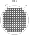
- FIG. 3 is a plan view schematically illustrating the configuration of the substrate W.
- the plurality of electronic devices D is formed the surface of the substrate W at predetermined intervals as illustrated in FIG. 3 .
- Electrodes E are formed on the electronic devices D, that is, on the surface of the substrate W.
- the electrodes E are electrically connected to circuit elements inside the electronic devices D, respectively. By applying a voltage to the electrodes E, a current can be flowed to the circuit elements inside the electronic devices D.
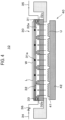
- FIG. 4 is a cross-sectional view schematically illustrating an upper configuration of the stage 10
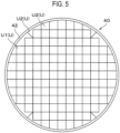
- FIG. 5 is a plan view schematically illustrating a configuration of the light irradiation mechanism 40 to be described later.
- the stage 10 has the placement table 30 and the light irradiation mechanism 40 in the order from the upper portion of the stage 10.
- the placement table 30 is a table on which the substrate W is placed.
- the light irradiation mechanism 40 irradiates a lid member 31 (to be described later) of the placement table 30 with light, thereby heating the substrate W and thus heating the electronic devices D formed on the substrate W.
- the placement table 30 has the lid member 31 provided on a placement side on which the substrate W is placed, that is, an upper side of the placement table 30, and a bottomed member 32 on a side of the placement table opposite to the substrate placement side of the placement table, that is, a lower side of the placement table 30.
- the lid member 31 and the bottomed member 32 are in contact with each other via an O-ring 33.
- the lid member 31 is formed in a disc shape and is made of, for example, SiC.
- SiC has high thermal conductivity and Young's modulus and also has high absorption efficiency for light from the light irradiation mechanism 40. Therefore, by forming the lid member 31 with SiC, it is possible to efficiently heat/cool the substrate W placed on the lid member 31 when the lid member 31 is heated/cooled. In addition, by forming the lid member 31 with SiC, it is possible to prevent the lid member 31 from being cracked. Further, it is possible to efficiently heat the lid member 31, that is, the substrate W, with the light from the light irradiation mechanism 40. Moreover, since a green sheet method or the like can be used for SiC, the workability is high and the manufacturing cost of the inspection apparatus 1 can be reduced.
- Suction holes (not shown) by which the substrate W is vacuum-suctioned are formed on the upper surface of the lid member 31. Further, a plurality of temperature sensors 31a is embedded in the lid member 31 at positions spaced apart from each other in a plan view.
- the bottomed member 32 is formed in a disk shape having substantially the same diameter as the lid member 31 and is formed of a light-transmissive member that transmits the light from the light irradiation mechanism 40.
- a light-transmissive member that transmits the light from the light irradiation mechanism 40.
- the light from the light irradiation mechanism 40 is near-infrared light
- polycarbonate, quartz, polyvinyl chloride, acrylic resin, or glass may be used as the light-transmissive member. Further, since it is easy to process and mold these materials, the manufacturing cost of the inspection apparatus 1 can be reduced.
- a groove for flowing refrigerant into the placement table 30 is formed on the upper surface of the bottomed member 32.
- the groove is covered with the lid member 31 to form a refrigerant flow path 32a.
- the placement table 30 has the refrigerant flow path 32a formed therein by the lid member 31 and the bottomed member 32.
- a supply port 32b and a discharge port 32c which communicate with the refrigerant flow path 32a, are formed on the side of the bottomed member 32.
- the supply port 32b is connected to a refrigerant pipe 34 for supplying the refrigerant to the refrigerant flow path 32a
- the discharge port 32c is connected to a discharge pipe 35 for discharging the refrigerant from the refrigerant flow path 32a.
- a flow rate control valve 36 that controls a flow rate of the refrigerant to be supplied to the refrigerant flow path 32a is provided in the refrigerant pipe 34.
- water which is a light-permeable liquid
- a pump (not shown) provided outside the inspection apparatus 1.
- the operation of the flow rate control valve 36 and the like for adjusting the flow rate of the refrigerant is controlled by the controller 13.
- a fluorocarbon refrigerant may be used as the refrigerant.
- the light irradiation mechanism 40 is disposed so as to face the surface of the placement table 30 opposite to the placement side of the substrate W, namely so as to face the lower surface of the bottomed member 32.
- the light irradiation mechanism 40 has a plurality of LEDs 41 provided to be oriented to the substrate W. Specifically, the light irradiation mechanism 40 has a plurality of LED units U in which the plurality of LEDs 41 is unitized, and has a base 42 having a surface on which the LED units U are mounted.
- the LED units U of the light irradiation mechanism 40 have units U1 each having a square shape in a plan view, which are arranged in the same number as the electronic devices D ( see FIG. 3 ) formed on the substrate W, and units U2 each having a non-rectangular shape in a plan view, which cover outer peripheries of the units U1. Further, the LED units U cover substantially the entire surface of the base 42 with the units U1 and U2 described above. Accordingly, at least the entire portion of the lid member 31 on which the substrate W is placed can be irradiated with light from the LEDs 41 of the LED units U.
- Each LED 41 irradiates the substrate W with light.
- each LED 41 emits near-infrared light.
- the light emitted from the LED 41 (hereinafter also referred to as "LED light") passes through the bottomed member 32 of the placement table 30, which is formed of a light-transmissive member.
- the light that has passed through the bottomed member 32 passes through the refrigerant that flows through the refrigerant flow path 32a of the placement table 30 and is capable of transmitting the light, and then is incident on the lid member 31.
- the light irradiation mechanism 40 the LED light incident on the lid member 31 on which the substrate W is placed in the placement table 30 is controlled on the basis of LED unit U. Therefore, the light irradiation mechanism 40 may irradiate only an arbitrary portion of the lid member 31 with the LED light, or may make the intensity of the irradiated light different between the arbitrary portion and the other portions.
- the inspection apparatus 1 controls such that the temperature of the electronic device D as inspection objects formed on the substrate W on the placement table 30 becomes constant at a target temperature by the heating by the light from the light irradiation mechanism 40 and the heat absorption by the refrigerant flowing through the refrigerant flow path 32a. For this temperature control, the inspection apparatus 1 measures the temperature of the electronic device D.
- FIG. 6 is a view schematically illustrating a configuration of a temperature measurement circuit of the electronic device D in the inspection apparatus 1.
- each probe 11a is connected to the tester 4 by a plurality of wirings 20 arranged on the interface 12.
- a relay 21 is provided on each of two wirings 20 that connect two probes 11a, which are in contact with two electrodes E of the potential difference generation circuit (for example, a diode) in the electronic device D, and the tester 4, among the wirings 20.
- Each relay 21 is configured to be able to switch and transmit the potential of each electrode E to either the tester 4 or the potential difference measurement unit 14. For example, each relay 21 transmits the potential of each electrode E to the potential difference measurement unit 14 at a predetermined timing after a mounting voltage is applied to each electrode E when inspecting the electrical characteristics of the electronic device D. It is known that in the above potential difference generation circuit, a potential difference generated when a predetermined current flows is different depending on the temperature. Therefore, the temperature of the electronic device D can be measured in real time during the inspection based on the potential difference of the potential difference generation circuit in the electronic device D, that is, the potential difference between the two electrodes E (probes 11a) of the potential difference generation circuit.
- the potential difference measurement unit 14 acquires the potential difference of the potential difference generation circuit in the electronic device D based on the potential of each electrode E transmitted from each relay 21, and further transmits the acquired potential difference to the controller 13.
- the controller 13 measures the temperature of the electronic device D based on the transmitted potential difference and the temperature characteristic of the potential difference of the potential difference generation circuit.
- the method of measuring the temperature of the electronic device D is not limited to the above, but any other methods may be used as long as the temperature of the electronic device D can be measured.
- FIG. 7 is a block diagram schematically illustrating an outline of the configuration of the controller 13.
- the controller 13 is composed of, for example, a computer, and has a program storage part (not shown).
- the program storage part stores programs and the like for controlling various processes such as the temperature control process and the like of the electronic device D in the inspection apparatus 1.
- the programs may be recorded in, for example, a computer-readable storage medium, and may be installed on the controller 13 from the storage medium.
- the controller 13 includes a storage part 13a, a temperature information acquisition part 13b, a temperature calculation part 13c, a heating controller 13d, a heat absorption controller 13e, and another temperature information acquisition part 13f.
- the storage part 13a stores the target temperature of the electronic device D, the temperature of the refrigerant, the maximum light output of the LED 41, and the like.
- the temperature of the refrigerant is determined in advance from, for example, the target temperature of the electronic device D, the maximum output of the LED 41, and the like.
- the storage part 13a also stores information on the temperature characteristics of the potential difference of the potential difference generation circuit in the electronic device D. Further, the storage part 13a stores calculation results of the temperature calculation part 13c and the like.
- the temperature information acquisition part 13b acquires, from the potential difference measurement part 14, the information on the potential difference of the above-mentioned potential difference generation circuit in the electronic device D as information on the temperature of the electronic device D as an inspection object at each time point during the inspection and until the end of the inspection.
- the temperature calculation part 13c calculates the temperature of the electronic device D based on the information on the potential difference of the potential difference generation circuit of the electronic device D as an inspection object, which is acquired by the temperature information acquisition part 13b at each time point during the inspection and until the end of the inspection, and the information on the temperature characteristic of the potential difference of the potential difference generation circuit.
- the temperature of the electronic device D calculated at each time point until the end of the inspection is stored in the storage part 13a for each inspection. That is, the transition of the temperature of the electronic device D is stored in the storage part 13a for each inspection.
- the heating controller 13d controls the light output from the LED 41 to control the heating of the electronic device D by the light from the LED 41.
- the heating controller 13d controls the light output from the LED 41 at the time of inspection by a closed loop control (for example, PID control) based on the temperature of the electronic device D as a current inspection object.
- the heating controller 13d determines the operation amount of the LED 41 at each point until the end of the inspection so that the temperature of the electronic device D as a current inspection object becomes constant at the target temperature. More specifically, the heating controller 13d calculates, for example, a deviation between the temperature of the electronic device D as an inspection object, which is calculated by the temperature calculation part 13c, and the target temperature of the electronic device D, which is stored in the storage part 13a.
- the heating controller 13d calculates/determines the operation amount of the LED 41 corresponding to the electronic device D as an inspection object from the deviation by the PID operation. Based on the calculated/determined operation amount, the heating controller 13d adjusts the light output of the corresponding LED 41. As a result, the heating of the electronic device D as an inspection object by the light from the LED 41 is controlled.
- the operation amount of the LED 41 calculated/determined at each time from the start of the inspection to the end of the inspection is converted into, for example, a heating amount (Q L ) by the light output from the LED 41 and stored in the storage part 13a for each inspection. That is, a transition of the heating amount (Q L ) by the light output from the LED 41 is stored in the storage part 13a for each inspection.
- the heat absorption controller 13e controls the flow rate of the refrigerant flowing through the refrigerant flow path 32a of the placement table 30. Based on a transition (profile) of a temperature (T D ) of the electronic device D in the inspection up to the n-th time, the heat absorption controller 13e estimates a transition of power (P E,n+1 ) applied from the tester 4 to the electronic device D at an (n+1)-th inspection. That is, based on the transition of the temperature (T D ) of the electronic device D in the past inspection, the heat absorption controller 13e estimates a transition of power (P E ) applied from the tester 4 to the electronic device D at the next inspection.
- the reason for estimating the transition of power (P E ) applied from the tester 4 to the electronic device D at the next inspection in this way is as follows. That is, the inspection includes a plurality of tests, powers applied to the electronic device D are different for each test, and the order of the tests may be changed by an operator of the inspection apparatus 1. This is because information on the test order and type is not transmitted to the controller 13. If the information on the test order and type is transmitted from the tester 4 to the controller 13, the inspection apparatus 1 can discriminate the test order and type to make a determination on the power transition without estimating.
- the heat absorption controller 13e controls the flow rate of the refrigerant flowing through the refrigerant flow path 32a of the placement table 30 at the time of the (n+1)-th inspection by an open loop control based on the estimated (n+1)-th transition of power (P E,n+1 ). Specifically, the opening degree of the flow rate control valve 36 at each time until the end of the inspection in the inspection up to the (n+1)-th time is calculated/determined based on the estimated (n+1)-th transition of power (P E,n+1 ). Then, the heat absorption controller 13e adjusts the flow rate of the refrigerant flowing through the refrigerant flow path 32a of the placement table 30 based on the calculated/determined opening degree of the flow rate control valve 36. As a result, the heat absorption of the electronic device D as an inspection object by the refrigerant is controlled.
- a range in which the temperature of the electronic device D can be adjusted to the target temperature by heating with the LED 41 is determined by the maximum output of the LED 41 and the density of the LED 41, but there are cases where the LED 41 having a small maximum output or a low density is used. Even in this case, as described above, by controlling the heat absorption based on the transition of power (P E ) at the time of the next inspection estimated from the past inspection, the temperature of the electronic device D can be adjusted to the target temperature by heating with the LED 41.
- the opening degree of the flow rate control valve 36 calculated/determined as described above at each time point until the end of the inspection is converted into, for example, the heat absorption amount (Q R ) by the refrigerant and stored in the storage part 13a for each inspection. That is, the transition of the heat absorption amount (Q R ) by the refrigerant is stored in the storage part 13a for each inspection.
- Another temperature information acquisition part 13f of the controller 13 acquires information on the temperature of the placement table 30, specifically, information on the temperature of the lid member 31, from the temperature sensor 31a.
- the power (P E,n ) applied from the tester 4 to the electronic device D at each time point of the n-th inspection, which is the past inspection, is proportional to the heat quantity (Q E,n ) radiated to the electronic device D by the power (P E,n ) at each time point of the n-th inspection.
- the heat quantity (Q ⁇ T,n ) that causes a temperature change ⁇ T in the electronic device D at each time point of the n-th inspection can be expressed by the following equation (1).
- Q ⁇ T , n Q L ,n ⁇ Q R , n + Q E ,n
- Q L,n represents the heating amount of the electronic device D as an inspection object by the light output from the LED 41 at each time point of the n-th inspection.
- Q R,n represents the heat absorption amount from the electronic device D as an inspection object by the refrigerant at each time point of the n-th inspection
- Q E,n represents the heat quantity radiated to the electronic device D by the power from the tester 4 at each time point of the n-th inspection.
- the temperature of the electronic device D at each time point is stored in the storage part 13a for each inspection.
- the heat quantity (Q ⁇ T ) that causes the temperature change ( ⁇ T) in the electronic device D at each time point can be calculated from the temperature of the electronic device D at each time point.
- the heating amount (Q L ) by the LED 41 at each time point and the heat absorption amount (Q R ) by the refrigerant at each time point are stored in the storage part 13a.
- the heat absorption controller 13e calculates the heat quantity (Q E,n ) radiated to the electronic device D by the power from the tester 4 at each time point of the n-th inspection.
- the power (P E ) from the tester 4 to the electronic device D is proportional to the heat quantity (Q E ) radiated to the electronic device D by the power (P E ). Therefore, the calculation of the heat quantity (Q E,n ) by the power from the tester 4 at each time point of the n-th inspection means that the power (P E,n ) applied from the tester 4 to the electronic device D can be calculated at each time point of the n-th inspection.
- the power to the electronic device D calculated at each time point until the end of the inspection is stored in the storage part 13a for each inspection.
- the heat absorption controller 13e estimates the power (P E,n+1 ) from the tester 4 to the electronic device D in the (n+1)-th inspection. That is, the transition of the power in the (n+1)-th inspection is estimated.
- the successive least squares method is used for the estimation.
- weighting can be increased for the calculation result of the power to the electronic device D in the new inspection and weighting can be decreased for the calculation result in the old inspection, so that more accurate estimation can be performed.
- the average value of the power from the tester 4 to the electronic device D in the inspection from a first inspection to a predetermined number of times of inspection may be calculated at each time point until the end of the inspection. Then, for the m-th (m>predetermined number of times) inspection, the power (P E,m ) from the tester 4 to the electronic device D in the inspection is estimated by the successive least squares method using the average value as an initial value.
- the heat absorption controller 13e controls, for example, the flow rate of the refrigerant flowing through the refrigerant flow path 32a of the placement table 30 to a predetermined flow rate.
- the predetermined number of times is, for example, the number of times the inspection of all the electronic devices D provided on the first substrate W is completed, or the number of times the inspection of all the substrates W of one lot is completed.
- the inspection may be terminated halfway before all the tests included in the inspection are completed. For example, when the temperature of the electronic device D as an inspection object is abnormal in the test before the last test included in the inspection, the inspection is ended halfway.
- P E transition of power
- the substrate W is taken out from the FOUP of the loader 3 and is transferred to and placed on the stage 10.
- the stage 10 is moved to a predetermined position.
- the potential difference measurement unit 14 acquires the potential difference of the above-mentioned potential difference generation circuit in the electronic device D as an inspection object. Then, assuming that the temperature of the lid member 31, which is made uniform in the plane, substantially matches the temperature of the electronic device D as an inspection object, the potential difference is calibrated, i.e., information on the temperature characteristics of the potential difference is corrected. The steps up to the correction are performed for each substrate W, for example.
- the stage 10 is moved, and the probe 11a installed above the stage 10 comes into contact with the electrode E of the electronic device D as an inspection object on the substrate W.
- a signal for inspection is input to the probe 11a.
- the inspection of the electronic device D is started.
- the temperature of the electronic device D as an inspection object is calculated from the information on the potential difference generated in the potential difference generation circuit of the electronic device D.
- the heating controller 13d controls the light output from the LED 41 of the LED unit U corresponding to the electronic device D by the closed loop control based on the temperature.
- the heat absorption controller 13e controls the flow rate of the refrigerant flowing through the refrigerant flow path 32a of the placement table 30 by the method described above.
- the steps after the calibration of the potential difference of the potential difference generation circuit in the electronic device D are repeated until the inspection of all the electronic devices D provided on the substrate W is completed.
- the transition of the temperature of the electronic device D as an inspection object, the transition of the heating amount by the light output from the LED 41, and the transition of the heat absorption amount of the refrigerant are stored in the storage part 13a for each inspection.
- the substrate W is returned to the FOUP of the loader 3, a subsequent substrate W is transferred to the stage 10. Thereafter, the above-described steps are executed until the inspection of all the substrates W is completed.
- the inspection apparatus 1 that inspects the electronic device D includes the placement table 30 on which the substrate W on which the electronic device D is provided is mounted, the placement table 30 being formed of the light-transmissive member on the side of the placement table opposite to the substrate placement side of the placement table and having therein the refrigerant flow path 32a through which the refrigerant capable of transmitting light flows, the light irradiation mechanism 40 that is disposed so as to face the surface of the side of the placement table 30 opposite to the substrate placement side of the placement table and has the plurality of LEDs 41 directed to the substrate W, and the controller 13 that controls the heat absorption by the refrigerant flowing through the refrigerant flow path 32a and the heating by the light from the LEDs 41 to control the temperature of the electronic device D as an inspection object, wherein the controller 13 includes the temperature information acquisition part 13b that acquires the information on the temperature of the electronic device D as an inspection object, the heating controller 13d that performs the control of the heating of the electronic device D as an
- the inspection apparatus 1 has the placement table 30 and the light irradiation mechanism 40 as described above, it is possible to cause the LED light from each LED 41 to reach the lid member 31 of the placement table 30 through the refrigerant or the like. Further, the light irradiation mechanism 40 can locally irradiate the lid member 31 with the LED light by the LED 41. If there is a configuration for controlling the heat absorption by the refrigerant, it may be conceivable to control the temperature of the electronic device D only by controlling the heat absorption by the refrigerant without depending on the control of the LED light. On the other hand, in the present embodiment, not only the heat absorption by the refrigerant but also the control by the LED light is performed to control the temperature of the electronic device D.
- the temperature of the electronic device D as an inspection object is controlled as described above, it is not necessary to use the LED 41 having a large maximum output or increase the density of the LED 41.
- the LED 41 having a large maximum output is expensive, and the cost increases if the density of the LED 41 is increased.
- the light irradiation mechanism 40 can locally change the intensity of light with which the lid member 31 is irradiated by each LED unit U. Therefore, it is possible to locally change the irradiation state of the lid member 31 with the LED light while cooling the lid member 31 entirely by the refrigerant in the placement table 30, and thus to set the heating state of the electronic device D as an inspection object to be different from other electronic devices. That is, it is possible to inspect the electronic device D as an inspection object while controlling both the temperature of the electronic device D as an inspection object and the temperature of the other electronic devices D on the substrate W.
- the heat absorption controller 13e controls the opening degree of the flow rate control valve 36 provided in the refrigerant pipe 34 that communicates with the refrigerant flow path 32a to adjust the flow rate of the refrigerant flowing through the refrigerant flow path 32a, and controls the heat absorption from the electronic device D as an inspection object by the refrigerant. Therefore, the responsiveness is higher than in a case where the heat absorption is controlled by adjusting the temperature of the refrigerant.
- the heat absorption controller 13e uses the successive least squares method to estimate the transition of the power applied to the electronic device D at the next inspection based on the transition of the temperature of the electronic device D in the past inspection. Therefore, the transition of the power can be accurately estimated. Further, since the heat absorption amount can be adjusted in advance based on the estimated value of the power applied to the electronic device D, the temperature control in a region where the controllability of the LED 41 is good becomes possible.
- water is used as the refrigerant that is required to absorb heat. Therefore, the heat absorption by the refrigerant can be carried out at a higher speed than in a case where a fluorocarbon refrigerant is used.
- the fluorocarbon refrigerant can also be used to control the temperature in a wider range.
- the temperature response characteristic is high.
Landscapes
- Engineering & Computer Science (AREA)
- Environmental & Geological Engineering (AREA)
- Physics & Mathematics (AREA)
- General Physics & Mathematics (AREA)
- Computer Hardware Design (AREA)
- Microelectronics & Electronic Packaging (AREA)
- General Engineering & Computer Science (AREA)
- Toxicology (AREA)
- Health & Medical Sciences (AREA)
- Testing Of Individual Semiconductor Devices (AREA)
- Testing Or Measuring Of Semiconductors Or The Like (AREA)
- Control Of Temperature (AREA)
- Sampling And Sample Adjustment (AREA)
Applications Claiming Priority (2)
| Application Number | Priority Date | Filing Date | Title |
|---|---|---|---|
| JP2018098705A JP7042158B2 (ja) | 2018-05-23 | 2018-05-23 | 検査装置及び温度制御方法 |
| PCT/JP2019/018537 WO2019225332A1 (ja) | 2018-05-23 | 2019-05-09 | 検査装置及び温度制御方法 |
Publications (3)
| Publication Number | Publication Date |
|---|---|
| EP3799111A1 EP3799111A1 (en) | 2021-03-31 |
| EP3799111A4 EP3799111A4 (en) | 2022-03-16 |
| EP3799111B1 true EP3799111B1 (en) | 2024-05-01 |
Family
ID=68617283
Family Applications (1)
| Application Number | Title | Priority Date | Filing Date |
|---|---|---|---|
| EP19807713.3A Active EP3799111B1 (en) | 2018-05-23 | 2019-05-09 | Inspection device and temperature control method |
Country Status (7)
| Country | Link |
|---|---|
| US (1) | US11385280B2 (ja) |
| EP (1) | EP3799111B1 (ja) |
| JP (1) | JP7042158B2 (ja) |
| KR (1) | KR102424608B1 (ja) |
| CN (1) | CN112119487A (ja) |
| TW (1) | TWI779195B (ja) |
| WO (1) | WO2019225332A1 (ja) |
Families Citing this family (6)
| Publication number | Priority date | Publication date | Assignee | Title |
|---|---|---|---|---|
| JP7380062B2 (ja) * | 2019-10-18 | 2023-11-15 | 富士電機株式会社 | 半導体モジュール |
| US11626184B2 (en) * | 2020-05-04 | 2023-04-11 | Nanya Technology Corporation | Apparatus for testing semiconductor device and method of testing thereof |
| TW202221306A (zh) * | 2020-07-29 | 2022-06-01 | 日商東京威力科創股份有限公司 | 基板處理裝置、及基板處理方法 |
| JP7449814B2 (ja) | 2020-08-12 | 2024-03-14 | 東京エレクトロン株式会社 | 検査方法及び検査装置 |
| JP2022092972A (ja) * | 2020-12-11 | 2022-06-23 | 東京エレクトロン株式会社 | 加熱装置及びledの制御方法 |
| CN116626475B (zh) * | 2023-07-20 | 2023-10-17 | 弘润半导体(苏州)有限公司 | 一种用于集成电路芯片的封装测试装置 |
Family Cites Families (17)
| Publication number | Priority date | Publication date | Assignee | Title |
|---|---|---|---|---|
| US5715051A (en) * | 1996-10-21 | 1998-02-03 | Medar, Inc. | Method and system for detecting defects in optically transmissive coatings formed on optical media substrates |
| JPH10135315A (ja) | 1996-10-29 | 1998-05-22 | Tokyo Electron Ltd | 試料載置台の温度制御装置及び検査装置 |
| JP2000340501A (ja) | 1999-04-07 | 2000-12-08 | Applied Materials Inc | 基板を熱処理する装置及び方法 |
| JP4659328B2 (ja) | 2002-10-21 | 2011-03-30 | 東京エレクトロン株式会社 | 被検査体を温度制御するプローブ装置 |
| KR100875527B1 (ko) * | 2003-08-18 | 2008-12-23 | 가부시키가이샤 아드반테스트 | 온도 제어 장치 및 온도 제어 방법 |
| JP5138253B2 (ja) * | 2006-09-05 | 2013-02-06 | 東京エレクトロン株式会社 | アニール装置 |
| US7860379B2 (en) * | 2007-01-15 | 2010-12-28 | Applied Materials, Inc. | Temperature measurement and control of wafer support in thermal processing chamber |
| JP5172615B2 (ja) | 2008-11-12 | 2013-03-27 | Ckd株式会社 | 温度制御装置 |
| JP4959669B2 (ja) * | 2008-12-05 | 2012-06-27 | 東京エレクトロン株式会社 | プローブ装置 |
| KR101125645B1 (ko) * | 2010-03-02 | 2012-03-27 | (주) 예스티 | 반도체 및 엘이디 웨이퍼 온도 제어 장치 |
| JP5732941B2 (ja) * | 2011-03-16 | 2015-06-10 | 東京エレクトロン株式会社 | プラズマエッチング装置及びプラズマエッチング方法 |
| JP5786487B2 (ja) * | 2011-06-22 | 2015-09-30 | 東京エレクトロン株式会社 | 熱処理装置及び熱処理方法 |
| JP2015056624A (ja) * | 2013-09-13 | 2015-03-23 | 東京エレクトロン株式会社 | 基板温調装置およびそれを用いた基板処理装置 |
| JP6423660B2 (ja) * | 2014-09-09 | 2018-11-14 | 東京エレクトロン株式会社 | ウエハ検査装置における検査用圧力設定値決定方法 |
| US20170032983A1 (en) * | 2015-07-29 | 2017-02-02 | Tokyo Electron Limited | Substrate processing apparatus, substrate processing method, maintenance method of substrate processing apparatus, and storage medium |
| US11221358B2 (en) * | 2017-03-21 | 2022-01-11 | Tokyo Electron Limited | Placement stand and electronic device inspecting apparatus |
| US11169204B2 (en) * | 2018-11-29 | 2021-11-09 | Tokyo Electron Limited | Temperature control device, temperature control method, and inspection apparatus |
-
2018
- 2018-05-23 JP JP2018098705A patent/JP7042158B2/ja active Active
-
2019
- 2019-05-09 WO PCT/JP2019/018537 patent/WO2019225332A1/ja unknown
- 2019-05-09 CN CN201980032631.2A patent/CN112119487A/zh active Pending
- 2019-05-09 KR KR1020207035759A patent/KR102424608B1/ko active IP Right Grant
- 2019-05-09 EP EP19807713.3A patent/EP3799111B1/en active Active
- 2019-05-09 US US17/056,524 patent/US11385280B2/en active Active
- 2019-05-20 TW TW108117261A patent/TWI779195B/zh active
Also Published As
| Publication number | Publication date |
|---|---|
| TW202013539A (zh) | 2020-04-01 |
| EP3799111A1 (en) | 2021-03-31 |
| KR20210010511A (ko) | 2021-01-27 |
| JP7042158B2 (ja) | 2022-03-25 |
| US20210208194A1 (en) | 2021-07-08 |
| EP3799111A4 (en) | 2022-03-16 |
| US11385280B2 (en) | 2022-07-12 |
| CN112119487A (zh) | 2020-12-22 |
| WO2019225332A1 (ja) | 2019-11-28 |
| TWI779195B (zh) | 2022-10-01 |
| KR102424608B1 (ko) | 2022-07-25 |
| JP2019204871A (ja) | 2019-11-28 |
Similar Documents
| Publication | Publication Date | Title |
|---|---|---|
| EP3799111B1 (en) | Inspection device and temperature control method | |
| US11340283B2 (en) | Testing device | |
| EP3550313B1 (en) | Electronic device inspecting apparatus | |
| US20080238466A1 (en) | Temperature sensing and prediction in ic sockets | |
| US11796400B2 (en) | Lifetime estimating system and method for heating source, and inspection apparatus | |
| US11221358B2 (en) | Placement stand and electronic device inspecting apparatus | |
| EP3882644B1 (en) | Substrate support, test device, and method of adjusting temperature of substrate support | |
| JP7449814B2 (ja) | 検査方法及び検査装置 | |
| KR102660269B1 (ko) | 가열 장치 및 led의 제어 방법 | |
| US20220128624A1 (en) | Placement table, testing device, and testing method | |
| KR100950701B1 (ko) | 메모리 모듈 실장 테스터용 가열장치 및 이를 이용한메모리 모듈 가열방법 |
Legal Events
| Date | Code | Title | Description |
|---|---|---|---|
| STAA | Information on the status of an ep patent application or granted ep patent |
Free format text: STATUS: THE INTERNATIONAL PUBLICATION HAS BEEN MADE |
|
| STAA | Information on the status of an ep patent application or granted ep patent |
Free format text: STATUS: THE INTERNATIONAL PUBLICATION HAS BEEN MADE |
|
| PUAI | Public reference made under article 153(3) epc to a published international application that has entered the european phase |
Free format text: ORIGINAL CODE: 0009012 |
|
| STAA | Information on the status of an ep patent application or granted ep patent |
Free format text: STATUS: REQUEST FOR EXAMINATION WAS MADE |
|
| 17P | Request for examination filed |
Effective date: 20201221 |
|
| AK | Designated contracting states |
Kind code of ref document: A1 Designated state(s): AL AT BE BG CH CY CZ DE DK EE ES FI FR GB GR HR HU IE IS IT LI LT LU LV MC MK MT NL NO PL PT RO RS SE SI SK SM TR |
|
| AX | Request for extension of the european patent |
Extension state: BA ME |
|
| DAV | Request for validation of the european patent (deleted) | ||
| DAX | Request for extension of the european patent (deleted) | ||
| A4 | Supplementary search report drawn up and despatched |
Effective date: 20220211 |
|
| RIC1 | Information provided on ipc code assigned before grant |
Ipc: G01R 31/28 20060101ALI20220207BHEP Ipc: H01L 21/66 20060101AFI20220207BHEP |
|
| GRAP | Despatch of communication of intention to grant a patent |
Free format text: ORIGINAL CODE: EPIDOSNIGR1 |
|
| STAA | Information on the status of an ep patent application or granted ep patent |
Free format text: STATUS: GRANT OF PATENT IS INTENDED |
|
| RIC1 | Information provided on ipc code assigned before grant |
Ipc: G01R 31/28 20060101ALI20231113BHEP Ipc: H01L 21/66 20060101AFI20231113BHEP |
|
| INTG | Intention to grant announced |
Effective date: 20231207 |
|
| GRAS | Grant fee paid |
Free format text: ORIGINAL CODE: EPIDOSNIGR3 |
|
| GRAA | (expected) grant |
Free format text: ORIGINAL CODE: 0009210 |
|
| STAA | Information on the status of an ep patent application or granted ep patent |
Free format text: STATUS: THE PATENT HAS BEEN GRANTED |
|
| AK | Designated contracting states |
Kind code of ref document: B1 Designated state(s): AL AT BE BG CH CY CZ DE DK EE ES FI FR GB GR HR HU IE IS IT LI LT LU LV MC MK MT NL NO PL PT RO RS SE SI SK SM TR |
|
| REG | Reference to a national code |
Ref country code: GB Ref legal event code: FG4D |
|
| REG | Reference to a national code |
Ref country code: CH Ref legal event code: EP |
|
| REG | Reference to a national code |
Ref country code: IE Ref legal event code: FG4D |
|
| REG | Reference to a national code |
Ref country code: DE Ref legal event code: R096 Ref document number: 602019051540 Country of ref document: DE |