EP3796551A1 - Elektronische schaltung zur frequenzverdreifachung, insbesondere für hochfrequenzanwendungen im millimeterwellenbereich - Google Patents
Elektronische schaltung zur frequenzverdreifachung, insbesondere für hochfrequenzanwendungen im millimeterwellenbereich Download PDFInfo
- Publication number
- EP3796551A1 EP3796551A1 EP20196153.9A EP20196153A EP3796551A1 EP 3796551 A1 EP3796551 A1 EP 3796551A1 EP 20196153 A EP20196153 A EP 20196153A EP 3796551 A1 EP3796551 A1 EP 3796551A1
- Authority
- EP
- European Patent Office
- Prior art keywords
- input
- coupled
- transistor
- circuit
- fraction
- Prior art date
- Legal status (The legal status is an assumption and is not a legal conclusion. Google has not performed a legal analysis and makes no representation as to the accuracy of the status listed.)
- Granted
Links
Images


Classifications
-
- H—ELECTRICITY
- H03—ELECTRONIC CIRCUITRY
- H03K—PULSE TECHNIQUE
- H03K5/00—Manipulating of pulses not covered by one of the other main groups of this subclass
- H03K5/00006—Changing the frequency
-
- H—ELECTRICITY
- H03—ELECTRONIC CIRCUITRY
- H03B—GENERATION OF OSCILLATIONS, DIRECTLY OR BY FREQUENCY-CHANGING, BY CIRCUITS EMPLOYING ACTIVE ELEMENTS WHICH OPERATE IN A NON-SWITCHING MANNER; GENERATION OF NOISE BY SUCH CIRCUITS
- H03B19/00—Generation of oscillations by non-regenerative frequency multiplication or division of a signal from a separate source
- H03B19/06—Generation of oscillations by non-regenerative frequency multiplication or division of a signal from a separate source by means of discharge device or semiconductor device with more than two electrodes
- H03B19/14—Generation of oscillations by non-regenerative frequency multiplication or division of a signal from a separate source by means of discharge device or semiconductor device with more than two electrodes by means of a semiconductor device
-
- H—ELECTRICITY
- H03—ELECTRONIC CIRCUITRY
- H03K—PULSE TECHNIQUE
- H03K17/00—Electronic switching or gating, i.e. not by contact-making and –breaking
- H03K17/51—Electronic switching or gating, i.e. not by contact-making and –breaking characterised by the components used
- H03K17/56—Electronic switching or gating, i.e. not by contact-making and –breaking characterised by the components used by the use, as active elements, of semiconductor devices
- H03K17/60—Electronic switching or gating, i.e. not by contact-making and –breaking characterised by the components used by the use, as active elements, of semiconductor devices the devices being bipolar transistors
Definitions
- the present invention relates to an electronic circuit for tripling frequency, in particular for radiofrequency applications in the millimeter wave range.
- a more promising approach consists in providing a PLL in a lower range (e.g., in the 10-20 GHz range), where the silicon VCO features the best figure of merit, followed by a frequency multiplier chain.
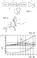
- Figure 1 shows a typical frequency multiplier system 1 for obtaining a multiplication by 6, for example for obtaining a 60GHz voltage from a 10 GHz source.
- a low-frequency voltage generator 2 supplies an input voltage Vin at a base frequency f 0 , e.g. at 10 GHz, to a frequency tripler 3, which generates an intermediate voltage V1 at a triple frequency (3f 0 ).
- the intermediate voltage V1 is available at a first output O1 through a first buffer 4 and fed to a frequency doubler 5 that generates an output voltage Vo at output frequency 6f 0 .
- the output voltage Vo is made available at a second output O2 through a second buffer 6.
- the frequency multiplier system 1 has to provide a good suppression of the driving signal and of undesired harmonics in order not to impair the transceiver performance.
- the first stage frequency tripler 3
- the first stage features the highest suppression, because its spurious tones are shifted close to the final LO frequencies by the intermodulation of the cascaded stages.
- this issue is more critical for odd-order multipliers, because even-order multipliers (here, the frequency doubler 5) may exploit push-push transistors for suppression of signal components at undesired frequencies.
- Odd-order multipliers such as the frequency tripler 3 of the frequency multiplier system 1, typically comprise a transistor with low conduction angle (e.g., class-C biased transistor) that generates a harmonic-rich current and the desired component is selected with a band-pass filter or an injection-locked oscillator.
- a transistor with low conduction angle e.g., class-C biased transistor
- FIG. 2 shows the basic structure of a class-C tripler circuit, indicated by 10.
- the transistor 11 has an emitter terminal E grounded, and a collector terminal C coupled to an output terminal 14 and to a supply voltage V cc through an LC resonant circuit 15 tuned at 3f 0 .
- the class-C tripler circuit 10 conducts a current Io whose harmonic content is set by the conduction angle ⁇ determined by the bias voltage Vb and shown in the simulations of Figures 3A and 3B .
- Figure 3A shows the plot of the output current density Jo (output current Io normalized to the area A of the transistor 11) for the fundamental (If0), the third harmonic (I3f0) and the fifth harmonic (I5f0).
- the total harmonic rejection ratio HRR is dominated by the fundamental Jf0, i.e. the leakage of the driving signal, which is always larger than the normalized third harmonic J3f0.
- the amplitude of normalized third harmonic J3f0 is maximized (point M in Figure 3A ), but the fundamental Jf0 is still 9 dB larger than the third harmonic J3f0 (as also visible in Figure 3B ).
- Even dimensioning the LC resonant circuit 15 to maximize suppression while compromising bandwidth, the class-C tripler circuit 10 has a very poor suppression, that cannot be increased over 20 dB.
- Class-C tripler circuits may be improved, in principle, by using a more complex filter topology or by cascading multiple filtering stages, but at the cost of a high design complexity, big area, bandwidth limitation and higher consumption.
- injection-locked oscillator solution (see, e.g., N. Mazor et al., "A high suppression frequency tripler for 60-GHz transceivers," in 2015 IEEE MTT-S International Microwave Symposium, 2015, pp. 1-4 ), although providing a better suppression (up to about 30dB), does not satisfactorily solve the problem.
- WO 2015/042814 A discloses a wideband injection locked frequency multiplier that uses higher-order LC tanks and that suffers of low total harmonic rejection ratio HRR.
- an aim of the invention is to provide a frequency tripler that overcomes the drawbacks of the prior art and in particular remarkably improves the suppression of the driving signal frequency at the output.
- Figure 4 shows a tripler circuit 20 that allows to obtain a high suppression of undesired harmonics.
- Figure 4 shows the structure of the tripler circuit 20 that has a trans-characteristics approximating the above polynomial trans-characteristics f(V in ), as discussed later on.
- the tripler circuit 20 comprises a first and a second pair of transistors, cross-coupled to each other.
- the first pair of transistors comprises a first and a second transistor Q1, Q2, here of the bipolar NPN-type
- the second pair of transistors comprises a third and a fourth transistor Q3, Q4, here also of the bipolar NPN-type.
- Transistors Q1-Q4 have same parameters, in particular same emitter area.
- the first and second transistors Q1, Q2 have emitter terminals coupled to each other and to a common node 21, base terminals coupled to a first and, respectively, a second input node 22, 23 and collector terminals coupled to a first and, respectively, a second output node 24, 25 supplying a first and, respectively, a second single-ended current I o- and I o+ .
- the third and fourth transistor Q3, Q4 have emitter terminals coupled to each other and to the common node 21, base terminals coupled to a third and, respectively, a fourth input node 27, 28, and collector terminals coupled to the second and, respectively, the first output node 25, 24.
- a biasing current source 26, configured to generate bias current Ib, is coupled between the common node 21 and ground.
- the first and the second input nodes 22, 23 receive each a fraction equal to 1/2 of the input voltage V in , in counter-phase, both reduced by a DC voltage (offset voltage V os ).
- the third and the fourth input nodes 27, 28 receive each an attenuation ⁇ /2 of the input voltage, in counter-phase, the attenuation ⁇ being selected so that, during operation, at low values of the input voltage V in and considering also the offset voltage V os , the first pair of transistors Q1, Q2 is still off, while the second pair of transistors Q3, Q4 are on, as discussed in detail below.
- the trans-characteristic of the tripler circuit 20 of Figure 4 is shown by curve A plotted in Figure 5 with dotted line as normalized output current I on versus normalized input voltage V in /A.
- Figure 5 shows also the ideal trans-characteristic (1) with continuous line B.
- the normalized output current I on is the differential current I o+ - I o+ , normalized with respect to its maximum amplitude (equal to I b ).
- V in ⁇ 2 V os 1 ⁇ ⁇
- the value of the offset voltage V os is obtained as a linear function of the amplitude A of the input voltage V in , based on condition (5).
- a non-optimal value of the attenuation ⁇ may be set, and the envelope detector operates as an open loop able to compensate and maintain the linear desired relationship of condition (5).
- Figure 6 shows a tripler circuit, indicated by 30, comprising the tripler 20 of figure 5 and an envelope detector.
- an input transformer T1 has a primary winding 31 coupled between a first and a second circuit input 32, 33 and a secondary winding 35 coupled between the input nodes 22, 23 of the tripler circuit 20.
- the secondary winding 35 has a central tap 36 connected to a first output 37 of an envelope detector 38 and set at a first biasing voltage Vb1.
- a voltage divider 40 of capacitive type is coupled between the input nodes 22, 23 of the tripler circuit 20 and comprises a first branch 41 and a second branch 42.
- the first branch 41 of the voltage divider 40 comprises a first capacitor 45, a first resistor 46, a second resistor 47 and a second capacitor 48 connected in series.
- the first and second capacitors 45, 48 have same capacitance C1; the first and second resistors 46, 47 have same resistance R.
- the first branch 41 has a central tap between the first and second resistors 46, 47 coupled to a second output 50 of the envelope detector 38, which generates a second biasing voltage Vb2.
- the first branch 41 also has a first intermediate node 51 between the first capacitor 45 and the first resistor 46 and a second intermediate node 52 between the second resistor 47 and the second capacitor 48.
- the voltage difference Vb2-Vb1 forms the offset voltage V os of the tripler 20 of Figure 5 .
- the second branch 42 of the voltage divider 40 comprises a third capacitor 54 coupled between the first and second intermediate nodes 51, 52.
- the third capacitor 54 has a capacitance C2.
- First and second intermediate nodes 51, 52 are also coupled to the third and, respectively, the fourth input node 27, 28 of the tripler circuit 20.
- the first and second input nodes 22, 23 of the tripler circuit 20 are also coupled to a first, respectively a second input 55, 56 of the envelope detector 38 through respective capacitors 57, 58.
- the tripler circuit 30 also comprises an output transformer T2 having a primary winding 61 coupled between the first and second output nods 24, 25 of the tripler 20 and a secondary winding 62 coupled between a first and second circuit outputs 64, 65; and an LC network 66 formed by a shunt capacitor 67 and a tail inductor 68 is coupled between the common node 21 of the tripler 20 and ground.
- the first and second circuit outputs 64, 65 may be connected to an output buffer similar to the first buffer 4 of frequency multiplier system 1 of figure 1 and/or to a frequency multiplier such as the frequency doubler 5 of the frequency multiplier system 1 of figure 1 .
- the first transformer T1 operates for line adaptation (as a balun transformer) and generates a differential signal (corresponding to input voltage V in of Figure 4 and thus identified with the same reference) directly applied on the first and second input nodes 22, 23 of the tripler circuit 20 (and thus on the base terminals of the first and second transistors Q1, Q2).
- the differential signal V in is reduced by the attenuation ⁇ by the capacitive divider 40 and applied to the third and fourth input nodes 27, 28 of the tripler circuit 20 (and thus on the base terminals of the third and fourth transistors Q3, Q4).
- the tail inductor 68 resonates with shunt equivalent capacitance existing at the common node 21 and the shunt capacitance 67 is sized sufficiently large to act as an AC-short at the operating frequency of common node 21, which is 2f0.
- LC network 66 allows the shunt parasitic capacitances at common node 21 to charge-discharge at high frequency using the current being exchanged with the tail inductor 68, hence not to lag behind the base voltages of the input transistors Q1-Q4 when operating at high input frequency.
- Figure 7 shows an exemplary implementation of envelope detector 38, generating the offset voltage V os that satisfies condition (5).
- envelope detector 38 comprises an input differential pair 70 formed by a fifth and a sixth transistor Q5 and Q6 and driven by the input voltage V in .
- a current source 71 generating a second reference current 2I REF , twice the reference current I REF , is coupled to the emitter terminals of the fifth and sixth transistors Q5 and Q6 and to an averaging RC filter 72.
- the averaging filter RC 72 includes an averaging resistor 73 having resistance R E and is coupled to a first voltage generating network 75.
- First voltage generating network 75 comprises a first current generating branch 76 and a first current mirroring branch 77.
- First current generating branch 76 includes a first current source 80 generating reference current I REF and a transistor Q7; first current mirroring branch 77 includes a transistor Q8 that is base-coupled to transistor Q7 of the first current generating branch 76, has a collector terminal forming first output 37 of the envelope detector 38 and generates the first biasing voltage Vb1.
- a second voltage generating network 81 having the same basic structure of the first voltage generating network 75, has coupled transistors Q9 and Q10 and generates the second biasing voltage Vb2 at a collector of transistor Q9 coupled to the second output 50 of the envelope detector 38.
- the second voltage generating network 81 also includes a second current source 82 generating the reference current I REF .
- a supply voltage V CC is applied to the collector terminals of the fifth and sixth transistors Q5 and Q6 and to supply nodes of the first and second voltage generating networks 75, 81.
- Supply voltage V CC is also applied to a central tap of the second transformer T2.
- All transistors Q5-Q10 in the envelope detector 38 share a same bias voltage V CM .
- MOSFET transistors M1, M2 in the first voltage generating network 75 mirror current I REF + I RE into a first output resistor 85 (coupled to the first output 37 of the envelope detector 38) with resistance R1, while MOSFET transistors M3, M4 in the second voltage generating network 81 mirror current I REF into a second output resistor 86 with resistance R2 (coupled to the second output 50 of the envelope detector 38).
- Vb 1 V CC ⁇ I REF + I RE ⁇ R 1
- Vb 2 V CC ⁇ I REF ⁇ R 2.
- the ratio R1/R E is designed such that V os satisfies condition (5), thus allowing to maintain good suppression of the fundamental frequency component independently from the amplitude of the input signal.
- Figure 8 shows the plot of the output power P 3f0 measured at 3f0 when the input power P in is swept at 12.5 GHz and the plot of the sum P sum of the output powers P f0 (measured at f 0 ) and P 5f0 (measured at 5f 0 ) obtained with the frequency tripler 20.
- the output power P 3f0 is higher than the sum power P sum of about 40 dBm in almost the entire input power range and in any case never lower than 36 dBm.
- the improvement of the tripler circuit 20 with respect to a conventional tripler using class-C operating transistors is also visible from Figure 9 , showing the output spectrum obtainable with the present frequency tripler 20 (curve Tr1_3f0), the undesired output spectrum at f 0 obtainable with a conventional tripler using class-C operating transistors (curve Tr2_f0) and the undesired output spectrum at f 0 obtainable with the present frequency tripler 20 (curve Tr1_f0).
- curve Tr1_f0 is 20 dB lower than curve Tr2_f0 and 40 dB lower than curve Tr1_3f0.
- the present tripler circuit is able to suppress undesired fundamental and harmonics in a much better way than with conventional circuits.
- the present tripler circuit operates at low power compared with conventional designs exploiting class-C transistors and filters.
- Figure 6 shows a circuit including means for generating the voltages applied to the control terminals of transistors Q1-Q4, these voltage sources may be integrated in a separate chip and belong on a separate circuit.
Landscapes
- Physics & Mathematics (AREA)
- Nonlinear Science (AREA)
- Amplifiers (AREA)
- Transmitters (AREA)
- Superheterodyne Receivers (AREA)
Applications Claiming Priority (1)
| Application Number | Priority Date | Filing Date | Title |
|---|---|---|---|
| IT102019000016871A IT201900016871A1 (it) | 2019-09-20 | 2019-09-20 | Circuito elettronico per triplicare la frequenza, in particolare per applicazioni in radiofrequenza nell'intervallo delle onde millimetriche |
Publications (2)
| Publication Number | Publication Date |
|---|---|
| EP3796551A1 true EP3796551A1 (de) | 2021-03-24 |
| EP3796551B1 EP3796551B1 (de) | 2023-11-08 |
Family
ID=69173329
Family Applications (1)
| Application Number | Title | Priority Date | Filing Date |
|---|---|---|---|
| EP20196153.9A Active EP3796551B1 (de) | 2019-09-20 | 2020-09-15 | Elektronische schaltung zur frequenzverdreifachung, insbesondere für hochfrequenzanwendungen im millimeterwellenbereich |
Country Status (4)
| Country | Link |
|---|---|
| US (2) | US11271552B2 (de) |
| EP (1) | EP3796551B1 (de) |
| CN (2) | CN112542994B (de) |
| IT (1) | IT201900016871A1 (de) |
Cited By (1)
| Publication number | Priority date | Publication date | Assignee | Title |
|---|---|---|---|---|
| US11601090B1 (en) | 2021-08-31 | 2023-03-07 | Intrinsix Corp. | Radio frequency tripler systems and methods thereof |
Families Citing this family (1)
| Publication number | Priority date | Publication date | Assignee | Title |
|---|---|---|---|---|
| CN115270896B (zh) * | 2022-09-28 | 2023-04-07 | 西华大学 | 一种用于识别航空发动机主轴承松动故障的智能诊断方法 |
Citations (2)
| Publication number | Priority date | Publication date | Assignee | Title |
|---|---|---|---|---|
| GB2283347A (en) * | 1993-10-29 | 1995-05-03 | Nec Corp | Analogue multiplier |
| WO2015042814A1 (en) | 2013-09-25 | 2015-04-02 | Huawei Technologies Co., Ltd. | Wideband injection locked frequency multipliers, oscillators and dividers using higher order lc resonant tank |
Family Cites Families (12)
| Publication number | Priority date | Publication date | Assignee | Title |
|---|---|---|---|---|
| JP3037004B2 (ja) * | 1992-12-08 | 2000-04-24 | 日本電気株式会社 | マルチプライヤ |
| CA2111945C (en) * | 1992-12-21 | 1997-12-09 | Katsuji Kimura | Analog multiplier using an octotail cell or a quadritail cell |
| US5552734A (en) * | 1993-10-27 | 1996-09-03 | Nec Corporation | Local oscillator frequency multiplier and mixing circuit comprising a squaring circuit |
| JP2541495B2 (ja) * | 1993-12-15 | 1996-10-09 | 日本電気株式会社 | Agc付き周波数逓倍・ミキサ回路 |
| JPH1093399A (ja) * | 1996-09-19 | 1998-04-10 | Toshiba Corp | 注入同期リング発振器 |
| US7759988B2 (en) * | 2007-12-21 | 2010-07-20 | Autoliv Asp, Inc. | Frequency multiplier |
| US8330506B2 (en) * | 2008-11-24 | 2012-12-11 | Freescale Semiconductor, Inc. | Frequency multiplier circuit |
| TWI422143B (zh) * | 2010-01-29 | 2014-01-01 | Univ Nat Chiao Tung | 一種倍頻裝置與其操作方法 |
| US8786330B1 (en) * | 2013-03-12 | 2014-07-22 | Infineon Technologies Ag | System and method for a frequency doubler |
| CN103475310B (zh) * | 2013-09-21 | 2017-01-11 | 复旦大学 | 一种低功耗注入锁定三倍频器 |
| CN103731103B (zh) * | 2014-01-17 | 2016-08-17 | 东南大学 | 一种全差分微波毫米波倍频器 |
| TWI563800B (en) * | 2015-03-19 | 2016-12-21 | Univ Nat Chunghsing | Divide-by-3 injection locked frequency divider implemented by cascoded cross-coupled transistors |
-
2019
- 2019-09-20 IT IT102019000016871A patent/IT201900016871A1/it unknown
-
2020
- 2020-09-15 EP EP20196153.9A patent/EP3796551B1/de active Active
- 2020-09-18 US US17/025,288 patent/US11271552B2/en active Active
- 2020-09-21 CN CN202010997959.2A patent/CN112542994B/zh active Active
- 2020-09-21 CN CN202410758984.3A patent/CN118539872A/zh active Pending
-
2022
- 2022-01-17 US US17/577,292 patent/US11658646B2/en active Active
Patent Citations (2)
| Publication number | Priority date | Publication date | Assignee | Title |
|---|---|---|---|---|
| GB2283347A (en) * | 1993-10-29 | 1995-05-03 | Nec Corp | Analogue multiplier |
| WO2015042814A1 (en) | 2013-09-25 | 2015-04-02 | Huawei Technologies Co., Ltd. | Wideband injection locked frequency multipliers, oscillators and dividers using higher order lc resonant tank |
Non-Patent Citations (1)
| Title |
|---|
| N. MAZOR ET AL.: "A high suppression frequency tripler for 60-GHz transceivers", 2015 IEEE MTT-S INTERNATIONAL MICROWAVE SYMPOSIUM, 2015, pages 1 - 4, XP033181292, DOI: 10.1109/MWSYM.2015.7166840 |
Cited By (1)
| Publication number | Priority date | Publication date | Assignee | Title |
|---|---|---|---|---|
| US11601090B1 (en) | 2021-08-31 | 2023-03-07 | Intrinsix Corp. | Radio frequency tripler systems and methods thereof |
Also Published As
| Publication number | Publication date |
|---|---|
| US20210091757A1 (en) | 2021-03-25 |
| EP3796551B1 (de) | 2023-11-08 |
| CN112542994B (zh) | 2024-06-25 |
| US20220140822A1 (en) | 2022-05-05 |
| US11658646B2 (en) | 2023-05-23 |
| US11271552B2 (en) | 2022-03-08 |
| CN118539872A (zh) | 2024-08-23 |
| IT201900016871A1 (it) | 2021-03-20 |
| CN112542994A (zh) | 2021-03-23 |
Similar Documents
| Publication | Publication Date | Title |
|---|---|---|
| CN100479323C (zh) | 振荡器、通信装置 | |
| US7545229B2 (en) | Tunable frequency, low phase noise and low thermal drift oscillator | |
| US10454419B2 (en) | Hybrid resonator based voltage controlled oscillator (VCO) | |
| EP3577756B1 (de) | Breitbandfrequenz-tripler | |
| US20120249250A1 (en) | Quadrature Voltage Controlled Oscillator | |
| US11632090B1 (en) | Push-push frequency doubling scheme and circuit based on complementary transistors | |
| US9537447B2 (en) | System and method for a voltage controlled oscillator | |
| US11658646B2 (en) | Electronic circuit for tripling frequency | |
| US8198945B2 (en) | Quadrature oscillator with high linearity | |
| US9099957B2 (en) | Voltage-controlled oscillators and related systems | |
| US8219054B2 (en) | Oscillating circuit and radio communication apparatus | |
| US6842081B2 (en) | Dual frequency voltage controlled oscillator circuit | |
| US20190229675A1 (en) | Multi-Stage Sub-THz Frequency Generator Incorporating Injection Locking | |
| US9106179B2 (en) | Voltage-controlled oscillators and related systems | |
| CN111342774A (zh) | 一种基于c类振荡器拓扑的双核压控振荡器 | |
| Al-Eryani et al. | Wideband 148–188 GHz push-push VCO using variable inductance and capacitance | |
| Kozhuharov et al. | A W-and G-band MMIC source using InP HBT technology | |
| Jamal et al. | A low-power K-band Colpitts VCO with 30% tuning range in a 130 nm SiGe BiCMOS technology | |
| US11239797B1 (en) | Regenerative frequency doubler | |
| Liu et al. | 64 to 86 GHz VCO utilizing push-push frequency doubling in a 80 GHz f T SiGe HBT technology | |
| JP2002217727A (ja) | 注入同期発振器、発振器、およびそれらを用いた高周波通信装置 | |
| Kusumanchi et al. | A 17 GHz Output PLL-Based Frequency Doubler with-60dBc Fundamental Spur | |
| Heydari | 10 Millimeter-Wave Frequency Synthesis Based on Frequency Multiplications | |
| Sachdev et al. | An Universal Microwave Solid State Local Oscillator | |
| Zhang et al. | Reconfigurable up-converter with image rejection |
Legal Events
| Date | Code | Title | Description |
|---|---|---|---|
| PUAI | Public reference made under article 153(3) epc to a published international application that has entered the european phase |
Free format text: ORIGINAL CODE: 0009012 |
|
| STAA | Information on the status of an ep patent application or granted ep patent |
Free format text: STATUS: THE APPLICATION HAS BEEN PUBLISHED |
|
| AK | Designated contracting states |
Kind code of ref document: A1 Designated state(s): AL AT BE BG CH CY CZ DE DK EE ES FI FR GB GR HR HU IE IS IT LI LT LU LV MC MK MT NL NO PL PT RO RS SE SI SK SM TR |
|
| AX | Request for extension of the european patent |
Extension state: BA ME |
|
| STAA | Information on the status of an ep patent application or granted ep patent |
Free format text: STATUS: REQUEST FOR EXAMINATION WAS MADE |
|
| 17P | Request for examination filed |
Effective date: 20210922 |
|
| RBV | Designated contracting states (corrected) |
Designated state(s): AL AT BE BG CH CY CZ DE DK EE ES FI FR GB GR HR HU IE IS IT LI LT LU LV MC MK MT NL NO PL PT RO RS SE SI SK SM TR |
|
| GRAP | Despatch of communication of intention to grant a patent |
Free format text: ORIGINAL CODE: EPIDOSNIGR1 |
|
| STAA | Information on the status of an ep patent application or granted ep patent |
Free format text: STATUS: GRANT OF PATENT IS INTENDED |
|
| INTG | Intention to grant announced |
Effective date: 20230601 |
|
| GRAS | Grant fee paid |
Free format text: ORIGINAL CODE: EPIDOSNIGR3 |
|
| GRAA | (expected) grant |
Free format text: ORIGINAL CODE: 0009210 |
|
| STAA | Information on the status of an ep patent application or granted ep patent |
Free format text: STATUS: THE PATENT HAS BEEN GRANTED |
|
| AK | Designated contracting states |
Kind code of ref document: B1 Designated state(s): AL AT BE BG CH CY CZ DE DK EE ES FI FR GB GR HR HU IE IS IT LI LT LU LV MC MK MT NL NO PL PT RO RS SE SI SK SM TR |
|
| REG | Reference to a national code |
Ref country code: GB Ref legal event code: FG4D |
|
| REG | Reference to a national code |
Ref country code: CH Ref legal event code: EP |
|
| REG | Reference to a national code |
Ref country code: DE Ref legal event code: R096 Ref document number: 602020020614 Country of ref document: DE |
|
| REG | Reference to a national code |
Ref country code: IE Ref legal event code: FG4D |
|
| REG | Reference to a national code |
Ref country code: LT Ref legal event code: MG9D |
|
| REG | Reference to a national code |
Ref country code: NL Ref legal event code: MP Effective date: 20231108 |
|
| PG25 | Lapsed in a contracting state [announced via postgrant information from national office to epo] |
Ref country code: GR Free format text: LAPSE BECAUSE OF FAILURE TO SUBMIT A TRANSLATION OF THE DESCRIPTION OR TO PAY THE FEE WITHIN THE PRESCRIBED TIME-LIMIT Effective date: 20240209 |
|
| PG25 | Lapsed in a contracting state [announced via postgrant information from national office to epo] |
Ref country code: IS Free format text: LAPSE BECAUSE OF FAILURE TO SUBMIT A TRANSLATION OF THE DESCRIPTION OR TO PAY THE FEE WITHIN THE PRESCRIBED TIME-LIMIT Effective date: 20240308 |
|
| PG25 | Lapsed in a contracting state [announced via postgrant information from national office to epo] |
Ref country code: LT Free format text: LAPSE BECAUSE OF FAILURE TO SUBMIT A TRANSLATION OF THE DESCRIPTION OR TO PAY THE FEE WITHIN THE PRESCRIBED TIME-LIMIT Effective date: 20231108 |
|
| REG | Reference to a national code |
Ref country code: AT Ref legal event code: MK05 Ref document number: 1630538 Country of ref document: AT Kind code of ref document: T Effective date: 20231108 |
|
| PG25 | Lapsed in a contracting state [announced via postgrant information from national office to epo] |
Ref country code: NL Free format text: LAPSE BECAUSE OF FAILURE TO SUBMIT A TRANSLATION OF THE DESCRIPTION OR TO PAY THE FEE WITHIN THE PRESCRIBED TIME-LIMIT Effective date: 20231108 |
|
| PG25 | Lapsed in a contracting state [announced via postgrant information from national office to epo] |
Ref country code: AT Free format text: LAPSE BECAUSE OF FAILURE TO SUBMIT A TRANSLATION OF THE DESCRIPTION OR TO PAY THE FEE WITHIN THE PRESCRIBED TIME-LIMIT Effective date: 20231108 |
|
| PG25 | Lapsed in a contracting state [announced via postgrant information from national office to epo] |
Ref country code: ES Free format text: LAPSE BECAUSE OF FAILURE TO SUBMIT A TRANSLATION OF THE DESCRIPTION OR TO PAY THE FEE WITHIN THE PRESCRIBED TIME-LIMIT Effective date: 20231108 |
|
| PG25 | Lapsed in a contracting state [announced via postgrant information from national office to epo] |
Ref country code: NL Free format text: LAPSE BECAUSE OF FAILURE TO SUBMIT A TRANSLATION OF THE DESCRIPTION OR TO PAY THE FEE WITHIN THE PRESCRIBED TIME-LIMIT Effective date: 20231108 Ref country code: LT Free format text: LAPSE BECAUSE OF FAILURE TO SUBMIT A TRANSLATION OF THE DESCRIPTION OR TO PAY THE FEE WITHIN THE PRESCRIBED TIME-LIMIT Effective date: 20231108 Ref country code: IS Free format text: LAPSE BECAUSE OF FAILURE TO SUBMIT A TRANSLATION OF THE DESCRIPTION OR TO PAY THE FEE WITHIN THE PRESCRIBED TIME-LIMIT Effective date: 20240308 Ref country code: GR Free format text: LAPSE BECAUSE OF FAILURE TO SUBMIT A TRANSLATION OF THE DESCRIPTION OR TO PAY THE FEE WITHIN THE PRESCRIBED TIME-LIMIT Effective date: 20240209 Ref country code: ES Free format text: LAPSE BECAUSE OF FAILURE TO SUBMIT A TRANSLATION OF THE DESCRIPTION OR TO PAY THE FEE WITHIN THE PRESCRIBED TIME-LIMIT Effective date: 20231108 Ref country code: BG Free format text: LAPSE BECAUSE OF FAILURE TO SUBMIT A TRANSLATION OF THE DESCRIPTION OR TO PAY THE FEE WITHIN THE PRESCRIBED TIME-LIMIT Effective date: 20240208 Ref country code: AT Free format text: LAPSE BECAUSE OF FAILURE TO SUBMIT A TRANSLATION OF THE DESCRIPTION OR TO PAY THE FEE WITHIN THE PRESCRIBED TIME-LIMIT Effective date: 20231108 Ref country code: PT Free format text: LAPSE BECAUSE OF FAILURE TO SUBMIT A TRANSLATION OF THE DESCRIPTION OR TO PAY THE FEE WITHIN THE PRESCRIBED TIME-LIMIT Effective date: 20240308 |
|
| PG25 | Lapsed in a contracting state [announced via postgrant information from national office to epo] |
Ref country code: SE Free format text: LAPSE BECAUSE OF FAILURE TO SUBMIT A TRANSLATION OF THE DESCRIPTION OR TO PAY THE FEE WITHIN THE PRESCRIBED TIME-LIMIT Effective date: 20231108 Ref country code: RS Free format text: LAPSE BECAUSE OF FAILURE TO SUBMIT A TRANSLATION OF THE DESCRIPTION OR TO PAY THE FEE WITHIN THE PRESCRIBED TIME-LIMIT Effective date: 20231108 Ref country code: PL Free format text: LAPSE BECAUSE OF FAILURE TO SUBMIT A TRANSLATION OF THE DESCRIPTION OR TO PAY THE FEE WITHIN THE PRESCRIBED TIME-LIMIT Effective date: 20231108 Ref country code: NO Free format text: LAPSE BECAUSE OF FAILURE TO SUBMIT A TRANSLATION OF THE DESCRIPTION OR TO PAY THE FEE WITHIN THE PRESCRIBED TIME-LIMIT Effective date: 20240208 Ref country code: LV Free format text: LAPSE BECAUSE OF FAILURE TO SUBMIT A TRANSLATION OF THE DESCRIPTION OR TO PAY THE FEE WITHIN THE PRESCRIBED TIME-LIMIT Effective date: 20231108 Ref country code: HR Free format text: LAPSE BECAUSE OF FAILURE TO SUBMIT A TRANSLATION OF THE DESCRIPTION OR TO PAY THE FEE WITHIN THE PRESCRIBED TIME-LIMIT Effective date: 20231108 |
|
| PG25 | Lapsed in a contracting state [announced via postgrant information from national office to epo] |
Ref country code: DK Free format text: LAPSE BECAUSE OF FAILURE TO SUBMIT A TRANSLATION OF THE DESCRIPTION OR TO PAY THE FEE WITHIN THE PRESCRIBED TIME-LIMIT Effective date: 20231108 |
|
| PG25 | Lapsed in a contracting state [announced via postgrant information from national office to epo] |
Ref country code: CZ Free format text: LAPSE BECAUSE OF FAILURE TO SUBMIT A TRANSLATION OF THE DESCRIPTION OR TO PAY THE FEE WITHIN THE PRESCRIBED TIME-LIMIT Effective date: 20231108 |
|
| PG25 | Lapsed in a contracting state [announced via postgrant information from national office to epo] |
Ref country code: SK Free format text: LAPSE BECAUSE OF FAILURE TO SUBMIT A TRANSLATION OF THE DESCRIPTION OR TO PAY THE FEE WITHIN THE PRESCRIBED TIME-LIMIT Effective date: 20231108 |
|
| PG25 | Lapsed in a contracting state [announced via postgrant information from national office to epo] |
Ref country code: SM Free format text: LAPSE BECAUSE OF FAILURE TO SUBMIT A TRANSLATION OF THE DESCRIPTION OR TO PAY THE FEE WITHIN THE PRESCRIBED TIME-LIMIT Effective date: 20231108 Ref country code: SK Free format text: LAPSE BECAUSE OF FAILURE TO SUBMIT A TRANSLATION OF THE DESCRIPTION OR TO PAY THE FEE WITHIN THE PRESCRIBED TIME-LIMIT Effective date: 20231108 Ref country code: RO Free format text: LAPSE BECAUSE OF FAILURE TO SUBMIT A TRANSLATION OF THE DESCRIPTION OR TO PAY THE FEE WITHIN THE PRESCRIBED TIME-LIMIT Effective date: 20231108 Ref country code: IT Free format text: LAPSE BECAUSE OF FAILURE TO SUBMIT A TRANSLATION OF THE DESCRIPTION OR TO PAY THE FEE WITHIN THE PRESCRIBED TIME-LIMIT Effective date: 20231108 Ref country code: EE Free format text: LAPSE BECAUSE OF FAILURE TO SUBMIT A TRANSLATION OF THE DESCRIPTION OR TO PAY THE FEE WITHIN THE PRESCRIBED TIME-LIMIT Effective date: 20231108 Ref country code: DK Free format text: LAPSE BECAUSE OF FAILURE TO SUBMIT A TRANSLATION OF THE DESCRIPTION OR TO PAY THE FEE WITHIN THE PRESCRIBED TIME-LIMIT Effective date: 20231108 Ref country code: CZ Free format text: LAPSE BECAUSE OF FAILURE TO SUBMIT A TRANSLATION OF THE DESCRIPTION OR TO PAY THE FEE WITHIN THE PRESCRIBED TIME-LIMIT Effective date: 20231108 |
|
| REG | Reference to a national code |
Ref country code: DE Ref legal event code: R097 Ref document number: 602020020614 Country of ref document: DE |
|
| PLBE | No opposition filed within time limit |
Free format text: ORIGINAL CODE: 0009261 |
|
| STAA | Information on the status of an ep patent application or granted ep patent |
Free format text: STATUS: NO OPPOSITION FILED WITHIN TIME LIMIT |
|
| 26N | No opposition filed |
Effective date: 20240809 |
|
| PG25 | Lapsed in a contracting state [announced via postgrant information from national office to epo] |
Ref country code: SI Free format text: LAPSE BECAUSE OF FAILURE TO SUBMIT A TRANSLATION OF THE DESCRIPTION OR TO PAY THE FEE WITHIN THE PRESCRIBED TIME-LIMIT Effective date: 20231108 |
|
| PG25 | Lapsed in a contracting state [announced via postgrant information from national office to epo] |
Ref country code: SI Free format text: LAPSE BECAUSE OF FAILURE TO SUBMIT A TRANSLATION OF THE DESCRIPTION OR TO PAY THE FEE WITHIN THE PRESCRIBED TIME-LIMIT Effective date: 20231108 |
|
| PG25 | Lapsed in a contracting state [announced via postgrant information from national office to epo] |
Ref country code: MC Free format text: LAPSE BECAUSE OF FAILURE TO SUBMIT A TRANSLATION OF THE DESCRIPTION OR TO PAY THE FEE WITHIN THE PRESCRIBED TIME-LIMIT Effective date: 20231108 |
|
| REG | Reference to a national code |
Ref country code: CH Ref legal event code: PL |
|
| PG25 | Lapsed in a contracting state [announced via postgrant information from national office to epo] |
Ref country code: LU Free format text: LAPSE BECAUSE OF NON-PAYMENT OF DUE FEES Effective date: 20240915 |
|
| GBPC | Gb: european patent ceased through non-payment of renewal fee |
Effective date: 20240915 |
|
| PG25 | Lapsed in a contracting state [announced via postgrant information from national office to epo] |
Ref country code: GB Free format text: LAPSE BECAUSE OF NON-PAYMENT OF DUE FEES Effective date: 20240915 |
|
| REG | Reference to a national code |
Ref country code: BE Ref legal event code: MM Effective date: 20240930 |
|
| PG25 | Lapsed in a contracting state [announced via postgrant information from national office to epo] |
Ref country code: BE Free format text: LAPSE BECAUSE OF NON-PAYMENT OF DUE FEES Effective date: 20240930 |
|
| PG25 | Lapsed in a contracting state [announced via postgrant information from national office to epo] |
Ref country code: FR Free format text: LAPSE BECAUSE OF NON-PAYMENT OF DUE FEES Effective date: 20240930 |
|
| PG25 | Lapsed in a contracting state [announced via postgrant information from national office to epo] |
Ref country code: CH Free format text: LAPSE BECAUSE OF NON-PAYMENT OF DUE FEES Effective date: 20240930 |
|
| PG25 | Lapsed in a contracting state [announced via postgrant information from national office to epo] |
Ref country code: IE Free format text: LAPSE BECAUSE OF NON-PAYMENT OF DUE FEES Effective date: 20240915 |
|
| PG25 | Lapsed in a contracting state [announced via postgrant information from national office to epo] |
Ref country code: FI Free format text: LAPSE BECAUSE OF FAILURE TO SUBMIT A TRANSLATION OF THE DESCRIPTION OR TO PAY THE FEE WITHIN THE PRESCRIBED TIME-LIMIT Effective date: 20231108 |
|
| PGFP | Annual fee paid to national office [announced via postgrant information from national office to epo] |
Ref country code: DE Payment date: 20250820 Year of fee payment: 6 |
|
| PG25 | Lapsed in a contracting state [announced via postgrant information from national office to epo] |
Ref country code: CY Free format text: LAPSE BECAUSE OF FAILURE TO SUBMIT A TRANSLATION OF THE DESCRIPTION OR TO PAY THE FEE WITHIN THE PRESCRIBED TIME-LIMIT; INVALID AB INITIO Effective date: 20200915 |
|
| PG25 | Lapsed in a contracting state [announced via postgrant information from national office to epo] |
Ref country code: HU Free format text: LAPSE BECAUSE OF FAILURE TO SUBMIT A TRANSLATION OF THE DESCRIPTION OR TO PAY THE FEE WITHIN THE PRESCRIBED TIME-LIMIT; INVALID AB INITIO Effective date: 20200915 |