EP3787134A1 - Optisches halbleiterbauelement und verfahren zur steuerung davon - Google Patents
Optisches halbleiterbauelement und verfahren zur steuerung davon Download PDFInfo
- Publication number
- EP3787134A1 EP3787134A1 EP19792161.2A EP19792161A EP3787134A1 EP 3787134 A1 EP3787134 A1 EP 3787134A1 EP 19792161 A EP19792161 A EP 19792161A EP 3787134 A1 EP3787134 A1 EP 3787134A1
- Authority
- EP
- European Patent Office
- Prior art keywords
- light beam
- etalon
- semiconductor device
- optical path
- tunable laser
- Prior art date
- Legal status (The legal status is an assumption and is not a legal conclusion. Google has not performed a legal analysis and makes no representation as to the accuracy of the status listed.)
- Withdrawn
Links
Images


Classifications
-
- H—ELECTRICITY
- H01—ELECTRIC ELEMENTS
- H01S—DEVICES USING THE PROCESS OF LIGHT AMPLIFICATION BY STIMULATED EMISSION OF RADIATION [LASER] TO AMPLIFY OR GENERATE LIGHT; DEVICES USING STIMULATED EMISSION OF ELECTROMAGNETIC RADIATION IN WAVE RANGES OTHER THAN OPTICAL
- H01S5/00—Semiconductor lasers
- H01S5/02—Structural details or components not essential to laser action
- H01S5/022—Mountings; Housings
- H01S5/0239—Combinations of electrical or optical elements
-
- H—ELECTRICITY
- H01—ELECTRIC ELEMENTS
- H01S—DEVICES USING THE PROCESS OF LIGHT AMPLIFICATION BY STIMULATED EMISSION OF RADIATION [LASER] TO AMPLIFY OR GENERATE LIGHT; DEVICES USING STIMULATED EMISSION OF ELECTROMAGNETIC RADIATION IN WAVE RANGES OTHER THAN OPTICAL
- H01S5/00—Semiconductor lasers
- H01S5/06—Arrangements for controlling the laser output parameters, e.g. by operating on the active medium
- H01S5/068—Stabilisation of laser output parameters
- H01S5/0683—Stabilisation of laser output parameters by monitoring the optical output parameters
- H01S5/0687—Stabilising the frequency of the laser
-
- H—ELECTRICITY
- H01—ELECTRIC ELEMENTS
- H01S—DEVICES USING THE PROCESS OF LIGHT AMPLIFICATION BY STIMULATED EMISSION OF RADIATION [LASER] TO AMPLIFY OR GENERATE LIGHT; DEVICES USING STIMULATED EMISSION OF ELECTROMAGNETIC RADIATION IN WAVE RANGES OTHER THAN OPTICAL
- H01S5/00—Semiconductor lasers
- H01S5/005—Optical components external to the laser cavity, specially adapted therefor, e.g. for homogenisation or merging of the beams or for manipulating laser pulses, e.g. pulse shaping
- H01S5/0071—Optical components external to the laser cavity, specially adapted therefor, e.g. for homogenisation or merging of the beams or for manipulating laser pulses, e.g. pulse shaping for beam steering, e.g. using a mirror outside the cavity to change the beam direction
-
- H—ELECTRICITY
- H01—ELECTRIC ELEMENTS
- H01S—DEVICES USING THE PROCESS OF LIGHT AMPLIFICATION BY STIMULATED EMISSION OF RADIATION [LASER] TO AMPLIFY OR GENERATE LIGHT; DEVICES USING STIMULATED EMISSION OF ELECTROMAGNETIC RADIATION IN WAVE RANGES OTHER THAN OPTICAL
- H01S5/00—Semiconductor lasers
- H01S5/10—Construction or shape of the optical resonator, e.g. extended or external cavity, coupled cavities, bent-guide, varying width, thickness or composition of the active region
- H01S5/14—External cavity lasers
- H01S5/141—External cavity lasers using a wavelength selective device, e.g. a grating or etalon
-
- H—ELECTRICITY
- H01—ELECTRIC ELEMENTS
- H01S—DEVICES USING THE PROCESS OF LIGHT AMPLIFICATION BY STIMULATED EMISSION OF RADIATION [LASER] TO AMPLIFY OR GENERATE LIGHT; DEVICES USING STIMULATED EMISSION OF ELECTROMAGNETIC RADIATION IN WAVE RANGES OTHER THAN OPTICAL
- H01S5/00—Semiconductor lasers
- H01S5/02—Structural details or components not essential to laser action
- H01S5/022—Mountings; Housings
- H01S5/02208—Mountings; Housings characterised by the shape of the housings
-
- H—ELECTRICITY
- H01—ELECTRIC ELEMENTS
- H01S—DEVICES USING THE PROCESS OF LIGHT AMPLIFICATION BY STIMULATED EMISSION OF RADIATION [LASER] TO AMPLIFY OR GENERATE LIGHT; DEVICES USING STIMULATED EMISSION OF ELECTROMAGNETIC RADIATION IN WAVE RANGES OTHER THAN OPTICAL
- H01S5/00—Semiconductor lasers
- H01S5/02—Structural details or components not essential to laser action
- H01S5/022—Mountings; Housings
- H01S5/023—Mount members, e.g. sub-mount members
- H01S5/02325—Mechanically integrated components on mount members or optical micro-benches
-
- H—ELECTRICITY
- H01—ELECTRIC ELEMENTS
- H01S—DEVICES USING THE PROCESS OF LIGHT AMPLIFICATION BY STIMULATED EMISSION OF RADIATION [LASER] TO AMPLIFY OR GENERATE LIGHT; DEVICES USING STIMULATED EMISSION OF ELECTROMAGNETIC RADIATION IN WAVE RANGES OTHER THAN OPTICAL
- H01S5/00—Semiconductor lasers
- H01S5/02—Structural details or components not essential to laser action
- H01S5/024—Arrangements for thermal management
- H01S5/02407—Active cooling, e.g. the laser temperature is controlled by a thermo-electric cooler or water cooling
- H01S5/02415—Active cooling, e.g. the laser temperature is controlled by a thermo-electric cooler or water cooling by using a thermo-electric cooler [TEC], e.g. Peltier element
-
- H—ELECTRICITY
- H01—ELECTRIC ELEMENTS
- H01S—DEVICES USING THE PROCESS OF LIGHT AMPLIFICATION BY STIMULATED EMISSION OF RADIATION [LASER] TO AMPLIFY OR GENERATE LIGHT; DEVICES USING STIMULATED EMISSION OF ELECTROMAGNETIC RADIATION IN WAVE RANGES OTHER THAN OPTICAL
- H01S5/00—Semiconductor lasers
- H01S5/02—Structural details or components not essential to laser action
- H01S5/024—Arrangements for thermal management
- H01S5/02438—Characterized by cooling of elements other than the laser chip, e.g. an optical element being part of an external cavity or a collimating lens
-
- H—ELECTRICITY
- H01—ELECTRIC ELEMENTS
- H01S—DEVICES USING THE PROCESS OF LIGHT AMPLIFICATION BY STIMULATED EMISSION OF RADIATION [LASER] TO AMPLIFY OR GENERATE LIGHT; DEVICES USING STIMULATED EMISSION OF ELECTROMAGNETIC RADIATION IN WAVE RANGES OTHER THAN OPTICAL
- H01S5/00—Semiconductor lasers
- H01S5/02—Structural details or components not essential to laser action
- H01S5/026—Monolithically integrated components, e.g. waveguides, monitoring photo-detectors, drivers
- H01S5/0261—Non-optical elements, e.g. laser driver components, heaters
-
- H—ELECTRICITY
- H01—ELECTRIC ELEMENTS
- H01S—DEVICES USING THE PROCESS OF LIGHT AMPLIFICATION BY STIMULATED EMISSION OF RADIATION [LASER] TO AMPLIFY OR GENERATE LIGHT; DEVICES USING STIMULATED EMISSION OF ELECTROMAGNETIC RADIATION IN WAVE RANGES OTHER THAN OPTICAL
- H01S5/00—Semiconductor lasers
- H01S5/06—Arrangements for controlling the laser output parameters, e.g. by operating on the active medium
- H01S5/0617—Arrangements for controlling the laser output parameters, e.g. by operating on the active medium using memorised or pre-programmed laser characteristics
-
- H—ELECTRICITY
- H01—ELECTRIC ELEMENTS
- H01S—DEVICES USING THE PROCESS OF LIGHT AMPLIFICATION BY STIMULATED EMISSION OF RADIATION [LASER] TO AMPLIFY OR GENERATE LIGHT; DEVICES USING STIMULATED EMISSION OF ELECTROMAGNETIC RADIATION IN WAVE RANGES OTHER THAN OPTICAL
- H01S5/00—Semiconductor lasers
- H01S5/06—Arrangements for controlling the laser output parameters, e.g. by operating on the active medium
- H01S5/068—Stabilisation of laser output parameters
- H01S5/0683—Stabilisation of laser output parameters by monitoring the optical output parameters
Definitions
- the present disclosure relates to an optical semiconductor device and a control method of the same.
- An optical semiconductor device in accordance with the present disclosure includes: a wavelength tunable laser element; a beam splitter that splits an outgoing beam of the wavelength tunable laser element into a first light beam and a second light beam parallel to each other, and outputs the first light beam and the second light beam; and an etalon that transmits the first light beam and the second light beam, wherein an optical path length to the first light beam of the etalon is different from an optical path length to the second light beam of the etalon.
- a control method of an optical semiconductor device in accordance with the present disclosure is a control method of an optical semiconductor device, the optical semiconductor device including a wavelength tunable laser element, a beam splitter that splits an outgoing beam of the wavelength tunable laser element into a first light beam and a second light beam parallel to each other and outputs the first light beam and the second light beam, an etalon that transmits the first light beam and the second light beam, a first detection unit that receives the first light beam that has passed through the etalon, a second detection unit that receives a second light beam that has passed through the etalon, and a third detection unit that receives another second light beam before passing through the etalon, wherein an optical path length to the first light beam of the etalon is different from an optical path length to the second light beam of the etalon, and the control method includes: a step of driving the wavelength tunable laser element in a driving condition corresponding to a target wavelength of the outgoing beam of the wavelength tunable laser element,
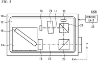
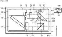
- FIG. 1A is a plan view illustrating an optical semiconductor device 100 in accordance with a first embodiment.
- the chain lines represent light beams.
- the X direction and the Y direction are at right angles to each other.
- the optical semiconductor device 100 includes a package 10, a thermoelectric cooler (TEC) 12, a carrier 14, a wavelength tunable laser element 16, a lens holder 18, beam splitters 20 and 22, an etalon 24, and light receiving elements 26, 28, and 30.
- TEC thermoelectric cooler
- the lens holder 18 is located at the negative X side of the output end of the wavelength tunable laser element 16, and the beam splitter 20 is located at the negative X side of the lens holder 18.
- the beam splitter 22 is located at the positive Y side of the beam splitter 20, and the light receiving element 30 is located at the positive Y side of the beam splitter 22.
- the etalon 24 is located at the positive X side of the beam splitter 22.
- the light receiving elements 26 and 28 are located at the positive X side of the etalon 24, and are arranged along the Y direction.
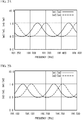
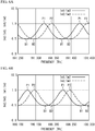
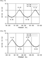
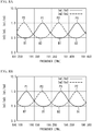
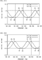
- FIG. 2A and FIG. 2B illustrate the transmission characteristics of the etalon 24.
- the transmission characteristics of the etalon 24 are determined by the optical path length of the light beam in the etalon 24 (the resonator length of the etalon 24), the refractive index of the etalon 24, and the incidence angle of the light beam.
- the optical path length of the light beam in the etalon 24 the resonator length of the etalon 24
- the refractive index of the etalon 24 the incidence angle of the light beam.
- desired transmission characteristics as illustrated in FIG. 2A and FIG. 2B Prior to description of the transmission characteristics in the first embodiment, comparative examples will be described.
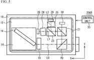
- FIG. 3 is a plan view illustrating an optical semiconductor device 100R in accordance with a first comparative example.
- a beam splitter 21 is located at the positive Y side of the beam splitter 20, and has one reflecting surface.
- the light receiving element 30 is located at the positive Y side of the beam splitter 20, and receives the light beam transmitted through the beam splitter 20.
- the etalon 24 and the light receiving element 26 are located at the positive X side of the beam splitter 21, and the light beam L1 enters the etalon 24.
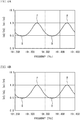
- the thickness (the optical path length) of the part through which the light beam L2 is transmitted of the etalon 24 is 0.97 mm + 0.14 ⁇ m, and is greater than 0.97 mm, which is the thickness of the part through which the light beam L1 is transmitted of the etalon 24, by 0.14 ⁇ m.
- This structure allows the transmission characteristic of the etalon 24 to the light beam L1 (corresponding to Im1/Im3) and the transmission characteristic of the etalon 24 to the light beam L2 (corresponding to Im2/Im3) to be adjusted to those illustrated in FIG. 2A and FIG. 2B .
- the ratio Im1/Im3 and the ratio Im2/Im3 have the same period, and are shifted from each other by approximately one-quarter period.
- the ratio Im2/Im3 exhibits a monotonic increase or a monotonic decrease.
- the wavelength is controlled using the ratio Im2/Im3.
- the ratio Im1/Im3 exhibits a monotonic increase or a monotonic decrease.
- the wavelength is controlled using the ratio Im1/Im3.
- the control unit 35 determines whether the temperature obtained from a temperature sensor (not illustrated) is within a setting range (step S28).
- the setting range is a predetermined range centered on the target temperatures of the wavelength tunable laser element 16 and the etalon.
- the control unit 35 changes the electric current value supplied to the TEC 12 so that the temperature TH becomes within the setting range.
- the control unit 35 executes the AFC and the APC in parallel. First, the AFC will be described.
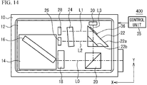
- the light beam L1 and the light beam L2 are nonparallel, and the incidence angle of the light beam L1 to the etalon 24 and the incidence angle of the light beam L2 to the etalon 24 are different from each other.
- the etalon 24 has a uniform thickness, but the incidence angles differ.
- the optical path length of the light beam L1 is different from the optical path length of the light beam L2.
- the transmission characteristic of the etalon 24 to the light beam L1 is different from the transmission characteristic of the etalon 24 to the light beam L2.
- the production tolerance and the variation in assembly can be reduced, and stable wavelength control is possible.
- the light beam L1 of which the polarization state has changed by reflection by the polarization reflector 36 enters the etalon 24.
- the polarization state of the light beam L1 is different from the polarization state of the light beam L2.
- the refractive index to the light beam L1 of the etalon 24 is different from the refractive index to the light beam L2.
- the beam splitter 42 Since the beam splitter 42 has different refractive indexes to the light beams having the polarization states different from each other, the emission direction of the light beam L1 and the emission direction of the light beam L2 are different from each other. Thus, as illustrated in FIG. 1B , the emission direction of the light beam L1 and the emission direction of the light beam L2 differ from each other by the angle ⁇ . Thus, the optical path (a first optical path) of the light beam L1 in the etalon 44 and the optical path (a second optical path) of the light beam L2 in the etalon 44 have optical path lengths different from each other. The incident directions in which the light beams L1 and L2 enter the beam splitter 42 are also different from each other.
- the variable polarizer 40 and the beam splitter 42 are located at the negative X side (the side toward which the laser beam is emitted) of the wavelength tunable laser element 16.
- the etalon 44 is located closer to the wavelength tunable laser element 16 than the variable polarizer 40 and the beam splitter 42 along the X-axis.
- the laser beam is emitted in the negative X direction from the wavelength tunable laser element 16, and propagates from the beam splitter 20 to the etalon 44 in the positive X direction.
- the optical semiconductor device 500 can be reduced in size.
Landscapes
- Physics & Mathematics (AREA)
- Condensed Matter Physics & Semiconductors (AREA)
- General Physics & Mathematics (AREA)
- Electromagnetism (AREA)
- Optics & Photonics (AREA)
- Semiconductor Lasers (AREA)
Applications Claiming Priority (3)
| Application Number | Priority Date | Filing Date | Title |
|---|---|---|---|
| JP2018085695 | 2018-04-26 | ||
| JP2019005113 | 2019-01-16 | ||
| PCT/JP2019/017263 WO2019208575A1 (ja) | 2018-04-26 | 2019-04-23 | 光半導体装置およびその制御方法 |
Publications (2)
| Publication Number | Publication Date |
|---|---|
| EP3787134A1 true EP3787134A1 (de) | 2021-03-03 |
| EP3787134A4 EP3787134A4 (de) | 2022-01-19 |
Family
ID=68294526
Family Applications (1)
| Application Number | Title | Priority Date | Filing Date |
|---|---|---|---|
| EP19792161.2A Withdrawn EP3787134A4 (de) | 2018-04-26 | 2019-04-23 | Optisches halbleiterbauelement und verfahren zur steuerung davon |
Country Status (5)
| Country | Link |
|---|---|
| US (1) | US11984699B2 (de) |
| EP (1) | EP3787134A4 (de) |
| JP (1) | JP7338938B2 (de) |
| CN (1) | CN112042067A (de) |
| WO (1) | WO2019208575A1 (de) |
Families Citing this family (1)
| Publication number | Priority date | Publication date | Assignee | Title |
|---|---|---|---|---|
| WO2024095424A1 (ja) * | 2022-11-02 | 2024-05-10 | 三菱電機株式会社 | 波長ロッカー及び波長ロッカー内蔵型波長可変光源 |
Family Cites Families (14)
| Publication number | Priority date | Publication date | Assignee | Title |
|---|---|---|---|---|
| DE19743493C2 (de) * | 1997-10-01 | 2001-02-22 | Mueller Wirts Thomas | Verfahren und Vorrichtung zur Laserfrequenzmessung und -Stabilisierung |
| US6233263B1 (en) * | 1999-06-04 | 2001-05-15 | Bandwidth9 | Monitoring and control assembly for wavelength stabilized optical system |
| US6822979B2 (en) * | 2001-07-06 | 2004-11-23 | Intel Corporation | External cavity laser with continuous tuning of grid generator |
| US6940879B2 (en) * | 2002-12-06 | 2005-09-06 | New Focus, Inc. | External cavity laser with dispersion compensation for mode-hop-free tuning |
| EP1432088A1 (de) * | 2002-12-19 | 2004-06-23 | Agilent Technologies, Inc. - a Delaware corporation - | Wellenlängenstabilisierung für eine Halbleiterlaserdiode |
| TW594364B (en) * | 2003-07-23 | 2004-06-21 | Delta Electronics Inc | Wavelength stabilizing apparatus and control method |
| US7327472B2 (en) * | 2004-07-23 | 2008-02-05 | Nusensors, Inc. | High temperature, minimally invasive optical sensing modules |
| US20060050747A1 (en) * | 2004-09-08 | 2006-03-09 | Trutna William R Jr | Frequency-tunable light sources and methods of generating frequency-tunable light |
| US7420686B2 (en) * | 2006-02-23 | 2008-09-02 | Picarro, Inc. | Wavelength measurement method based on combination of two signals in quadrature |
| US7633624B1 (en) * | 2006-11-06 | 2009-12-15 | Itt Manufacturing Enterprises, Inc. | Self compensating cube corner interferometer |
| JP2010034114A (ja) | 2008-07-25 | 2010-02-12 | Mitsubishi Electric Corp | レーザ装置、レーザモジュールおよび波長多重光通信システム |
| JP2014165384A (ja) * | 2013-02-26 | 2014-09-08 | Furukawa Electric Co Ltd:The | 半導体レーザモジュール |
| JP6176784B2 (ja) | 2013-09-19 | 2017-08-09 | 住友電気工業株式会社 | 波長制御システムおよび波長制御方法 |
| US10050405B2 (en) | 2016-04-19 | 2018-08-14 | Lumentum Operations Llc | Wavelength locker using multiple feedback curves to wavelength lock a beam |
-
2019
- 2019-04-23 US US17/049,512 patent/US11984699B2/en active Active
- 2019-04-23 CN CN201980027980.5A patent/CN112042067A/zh active Pending
- 2019-04-23 WO PCT/JP2019/017263 patent/WO2019208575A1/ja not_active Ceased
- 2019-04-23 JP JP2020515489A patent/JP7338938B2/ja active Active
- 2019-04-23 EP EP19792161.2A patent/EP3787134A4/de not_active Withdrawn
Also Published As
| Publication number | Publication date |
|---|---|
| EP3787134A4 (de) | 2022-01-19 |
| CN112042067A (zh) | 2020-12-04 |
| JPWO2019208575A1 (ja) | 2021-04-30 |
| WO2019208575A1 (ja) | 2019-10-31 |
| US20210242658A1 (en) | 2021-08-05 |
| JP7338938B2 (ja) | 2023-09-05 |
| US11984699B2 (en) | 2024-05-14 |
Similar Documents
| Publication | Publication Date | Title |
|---|---|---|
| US5418802A (en) | Frequency tunable waveguide extended cavity laser | |
| CN100511879C (zh) | 可调谐激光器、光模块及它们的控制方法 | |
| US6205159B1 (en) | Discrete wavelength liquid crystal tuned external cavity diode laser | |
| EP1601071B1 (de) | Wellenlängenabstimmbare Laservorrichtung | |
| US20020054614A1 (en) | Wavelength discretely tunable semiconductor laser | |
| WO2011120246A1 (zh) | 可调谐激光器 | |
| WO2011134177A1 (zh) | 可调谐激光器 | |
| US7701983B2 (en) | Tunable resonator, tunable light source using the same, and method for tuning wavelength of multiple resonator | |
| US20130163621A1 (en) | External cavity tunable laser module | |
| US5956356A (en) | Monitoring wavelength of laser devices | |
| JP2012119482A (ja) | 波長可変レーザ装置およびその制御方法 | |
| US20050276303A1 (en) | External Cavity Laser | |
| US20210036489A1 (en) | Narrow linewidth external cavity laser and optical module | |
| EP3787134A1 (de) | Optisches halbleiterbauelement und verfahren zur steuerung davon | |
| CN112397993A (zh) | 一种窄线宽外腔激光器及光模块 | |
| JP2002303904A (ja) | 光波長変換装置およびその調整方法 | |
| US11705692B2 (en) | Laser side mode suppression ratio control | |
| JP5333238B2 (ja) | 波長可変レーザ装置及びその波長切替方法 | |
| WO2019117044A1 (ja) | 光モジュール | |
| JPH11233894A (ja) | 波長可変外部共振器型レーザ | |
| US7283302B2 (en) | Wavelength filter and wavelength monitor device | |
| US20070041081A1 (en) | High performance compact external cavity laser( ecl) for telecomm applications | |
| JP2019106442A (ja) | 光モジュール | |
| JP2009016702A (ja) | 複屈折フィルタおよび固体レーザ装置 | |
| JPH06175175A (ja) | 第二高調波発生装置 |
Legal Events
| Date | Code | Title | Description |
|---|---|---|---|
| STAA | Information on the status of an ep patent application or granted ep patent |
Free format text: STATUS: THE INTERNATIONAL PUBLICATION HAS BEEN MADE |
|
| PUAI | Public reference made under article 153(3) epc to a published international application that has entered the european phase |
Free format text: ORIGINAL CODE: 0009012 |
|
| STAA | Information on the status of an ep patent application or granted ep patent |
Free format text: STATUS: REQUEST FOR EXAMINATION WAS MADE |
|
| 17P | Request for examination filed |
Effective date: 20201020 |
|
| AK | Designated contracting states |
Kind code of ref document: A1 Designated state(s): AL AT BE BG CH CY CZ DE DK EE ES FI FR GB GR HR HU IE IS IT LI LT LU LV MC MK MT NL NO PL PT RO RS SE SI SK SM TR |
|
| AX | Request for extension of the european patent |
Extension state: BA ME |
|
| DAV | Request for validation of the european patent (deleted) | ||
| DAX | Request for extension of the european patent (deleted) | ||
| A4 | Supplementary search report drawn up and despatched |
Effective date: 20211217 |
|
| RIC1 | Information provided on ipc code assigned before grant |
Ipc: H01S 5/024 20060101ALN20211213BHEP Ipc: H01S 5/022 20210101ALN20211213BHEP Ipc: H01S 5/0687 20060101AFI20211213BHEP |
|
| STAA | Information on the status of an ep patent application or granted ep patent |
Free format text: STATUS: THE APPLICATION IS DEEMED TO BE WITHDRAWN |
|
| 18D | Application deemed to be withdrawn |
Effective date: 20220723 |