EP3768465B1 - Verfahren zur herstellung eines fahrzeugbauteils aus glas - Google Patents
Verfahren zur herstellung eines fahrzeugbauteils aus glas Download PDFInfo
- Publication number
- EP3768465B1 EP3768465B1 EP19712053.8A EP19712053A EP3768465B1 EP 3768465 B1 EP3768465 B1 EP 3768465B1 EP 19712053 A EP19712053 A EP 19712053A EP 3768465 B1 EP3768465 B1 EP 3768465B1
- Authority
- EP
- European Patent Office
- Prior art keywords
- lead
- production method
- solder
- free solder
- block
- Prior art date
- Legal status (The legal status is an assumption and is not a legal conclusion. Google has not performed a legal analysis and makes no representation as to the accuracy of the status listed.)
- Active
Links
Images


Classifications
-
- B—PERFORMING OPERATIONS; TRANSPORTING
- B23—MACHINE TOOLS; METAL-WORKING NOT OTHERWISE PROVIDED FOR
- B23K—SOLDERING OR UNSOLDERING; WELDING; CLADDING OR PLATING BY SOLDERING OR WELDING; CUTTING BY APPLYING HEAT LOCALLY, e.g. FLAME CUTTING; WORKING BY LASER BEAM
- B23K1/00—Soldering, e.g. brazing, or unsoldering
- B23K1/0008—Soldering, e.g. brazing, or unsoldering specially adapted for particular articles or work
-
- B—PERFORMING OPERATIONS; TRANSPORTING
- B22—CASTING; POWDER METALLURGY
- B22F—WORKING METALLIC POWDER; MANUFACTURE OF ARTICLES FROM METALLIC POWDER; MAKING METALLIC POWDER; APPARATUS OR DEVICES SPECIALLY ADAPTED FOR METALLIC POWDER
- B22F7/00—Manufacture of composite layers, workpieces, or articles, comprising metallic powder, by sintering the powder, with or without compacting wherein at least one part is obtained by sintering or compression
- B22F7/06—Manufacture of composite layers, workpieces, or articles, comprising metallic powder, by sintering the powder, with or without compacting wherein at least one part is obtained by sintering or compression of composite workpieces or articles from parts, e.g. to form tipped tools
- B22F7/08—Manufacture of composite layers, workpieces, or articles, comprising metallic powder, by sintering the powder, with or without compacting wherein at least one part is obtained by sintering or compression of composite workpieces or articles from parts, e.g. to form tipped tools with one or more parts not made from powder
-
- B—PERFORMING OPERATIONS; TRANSPORTING
- B23—MACHINE TOOLS; METAL-WORKING NOT OTHERWISE PROVIDED FOR
- B23K—SOLDERING OR UNSOLDERING; WELDING; CLADDING OR PLATING BY SOLDERING OR WELDING; CUTTING BY APPLYING HEAT LOCALLY, e.g. FLAME CUTTING; WORKING BY LASER BEAM
- B23K35/00—Rods, electrodes, materials, or media, for use in soldering, welding, or cutting
- B23K35/02—Rods, electrodes, materials, or media, for use in soldering, welding, or cutting characterised by mechanical features, e.g. shape
- B23K35/0222—Rods, electrodes, materials, or media, for use in soldering, welding, or cutting characterised by mechanical features, e.g. shape for use in soldering, brazing
- B23K35/0244—Powders, particles or spheres; Preforms made therefrom
- B23K35/025—Pastes, creams, slurries
-
- B—PERFORMING OPERATIONS; TRANSPORTING
- B23—MACHINE TOOLS; METAL-WORKING NOT OTHERWISE PROVIDED FOR
- B23K—SOLDERING OR UNSOLDERING; WELDING; CLADDING OR PLATING BY SOLDERING OR WELDING; CUTTING BY APPLYING HEAT LOCALLY, e.g. FLAME CUTTING; WORKING BY LASER BEAM
- B23K35/00—Rods, electrodes, materials, or media, for use in soldering, welding, or cutting
- B23K35/22—Rods, electrodes, materials, or media, for use in soldering, welding, or cutting characterised by the composition or nature of the material
- B23K35/24—Selection of soldering or welding materials proper
- B23K35/26—Selection of soldering or welding materials proper with the principal constituent melting at less than 400 degrees C
- B23K35/262—Sn as the principal constituent
-
- B—PERFORMING OPERATIONS; TRANSPORTING
- B23—MACHINE TOOLS; METAL-WORKING NOT OTHERWISE PROVIDED FOR
- B23K—SOLDERING OR UNSOLDERING; WELDING; CLADDING OR PLATING BY SOLDERING OR WELDING; CUTTING BY APPLYING HEAT LOCALLY, e.g. FLAME CUTTING; WORKING BY LASER BEAM
- B23K35/00—Rods, electrodes, materials, or media, for use in soldering, welding, or cutting
- B23K35/22—Rods, electrodes, materials, or media, for use in soldering, welding, or cutting characterised by the composition or nature of the material
- B23K35/24—Selection of soldering or welding materials proper
- B23K35/30—Selection of soldering or welding materials proper with the principal constituent melting at less than 1550 degrees C
- B23K35/3006—Ag as the principal constituent
-
- C—CHEMISTRY; METALLURGY
- C22—METALLURGY; FERROUS OR NON-FERROUS ALLOYS; TREATMENT OF ALLOYS OR NON-FERROUS METALS
- C22C—ALLOYS
- C22C13/00—Alloys based on tin
-
- C—CHEMISTRY; METALLURGY
- C22—METALLURGY; FERROUS OR NON-FERROUS ALLOYS; TREATMENT OF ALLOYS OR NON-FERROUS METALS
- C22C—ALLOYS
- C22C19/00—Alloys based on nickel or cobalt
- C22C19/03—Alloys based on nickel or cobalt based on nickel
-
- H—ELECTRICITY
- H01—ELECTRIC ELEMENTS
- H01R—ELECTRICALLY-CONDUCTIVE CONNECTIONS; STRUCTURAL ASSOCIATIONS OF A PLURALITY OF MUTUALLY-INSULATED ELECTRICAL CONNECTING ELEMENTS; COUPLING DEVICES; CURRENT COLLECTORS
- H01R12/00—Structural associations of a plurality of mutually-insulated electrical connecting elements, specially adapted for printed circuits, e.g. printed circuit boards [PCB], flat or ribbon cables, or like generally planar structures, e.g. terminal strips, terminal blocks; Coupling devices specially adapted for printed circuits, flat or ribbon cables, or like generally planar structures; Terminals specially adapted for contact with, or insertion into, printed circuits, flat or ribbon cables, or like generally planar structures
- H01R12/50—Fixed connections
- H01R12/51—Fixed connections for rigid printed circuits or like structures
- H01R12/53—Fixed connections for rigid printed circuits or like structures connecting to cables except for flat or ribbon cables
-
- H—ELECTRICITY
- H01—ELECTRIC ELEMENTS
- H01R—ELECTRICALLY-CONDUCTIVE CONNECTIONS; STRUCTURAL ASSOCIATIONS OF A PLURALITY OF MUTUALLY-INSULATED ELECTRICAL CONNECTING ELEMENTS; COUPLING DEVICES; CURRENT COLLECTORS
- H01R12/00—Structural associations of a plurality of mutually-insulated electrical connecting elements, specially adapted for printed circuits, e.g. printed circuit boards [PCB], flat or ribbon cables, or like generally planar structures, e.g. terminal strips, terminal blocks; Coupling devices specially adapted for printed circuits, flat or ribbon cables, or like generally planar structures; Terminals specially adapted for contact with, or insertion into, printed circuits, flat or ribbon cables, or like generally planar structures
- H01R12/50—Fixed connections
- H01R12/51—Fixed connections for rigid printed circuits or like structures
- H01R12/55—Fixed connections for rigid printed circuits or like structures characterised by the terminals
- H01R12/57—Fixed connections for rigid printed circuits or like structures characterised by the terminals surface mounting terminals
-
- H—ELECTRICITY
- H01—ELECTRIC ELEMENTS
- H01R—ELECTRICALLY-CONDUCTIVE CONNECTIONS; STRUCTURAL ASSOCIATIONS OF A PLURALITY OF MUTUALLY-INSULATED ELECTRICAL CONNECTING ELEMENTS; COUPLING DEVICES; CURRENT COLLECTORS
- H01R4/00—Electrically-conductive connections between two or more conductive members in direct contact, i.e. touching one another; Means for effecting or maintaining such contact; Electrically-conductive connections having two or more spaced connecting locations for conductors and using contact members penetrating insulation
- H01R4/58—Electrically-conductive connections between two or more conductive members in direct contact, i.e. touching one another; Means for effecting or maintaining such contact; Electrically-conductive connections having two or more spaced connecting locations for conductors and using contact members penetrating insulation characterised by the form or material of the contacting members
- H01R4/62—Connections between conductors of different materials; Connections between or with aluminium or steel-core aluminium conductors
- H01R4/625—Soldered or welded connections
-
- H—ELECTRICITY
- H01—ELECTRIC ELEMENTS
- H01R—ELECTRICALLY-CONDUCTIVE CONNECTIONS; STRUCTURAL ASSOCIATIONS OF A PLURALITY OF MUTUALLY-INSULATED ELECTRICAL CONNECTING ELEMENTS; COUPLING DEVICES; CURRENT COLLECTORS
- H01R43/00—Apparatus or processes specially adapted for manufacturing, assembling, maintaining, or repairing of line connectors or current collectors or for joining electric conductors
- H01R43/02—Apparatus or processes specially adapted for manufacturing, assembling, maintaining, or repairing of line connectors or current collectors or for joining electric conductors for soldered or welded connections
-
- H—ELECTRICITY
- H05—ELECTRIC TECHNIQUES NOT OTHERWISE PROVIDED FOR
- H05B—ELECTRIC HEATING; ELECTRIC LIGHT SOURCES NOT OTHERWISE PROVIDED FOR; CIRCUIT ARRANGEMENTS FOR ELECTRIC LIGHT SOURCES, IN GENERAL
- H05B3/00—Ohmic-resistance heating
- H05B3/84—Heating arrangements specially adapted for transparent or reflecting areas, e.g. for demisting or de-icing windows, mirrors or vehicle windshields
-
- H—ELECTRICITY
- H01—ELECTRIC ELEMENTS
- H01Q—ANTENNAS, i.e. RADIO AERIALS
- H01Q1/00—Details of, or arrangements associated with, antennas
- H01Q1/12—Supports; Mounting means
- H01Q1/1271—Supports; Mounting means for mounting on windscreens
- H01Q1/1278—Supports; Mounting means for mounting on windscreens in association with heating wires or layers
-
- H—ELECTRICITY
- H01—ELECTRIC ELEMENTS
- H01Q—ANTENNAS, i.e. RADIO AERIALS
- H01Q1/00—Details of, or arrangements associated with, antennas
- H01Q1/36—Structural form of radiating elements, e.g. cone, spiral, umbrella; Particular materials used therewith
- H01Q1/364—Structural form of radiating elements, e.g. cone, spiral, umbrella; Particular materials used therewith using a particular conducting material, e.g. superconductor
-
- H—ELECTRICITY
- H01—ELECTRIC ELEMENTS
- H01R—ELECTRICALLY-CONDUCTIVE CONNECTIONS; STRUCTURAL ASSOCIATIONS OF A PLURALITY OF MUTUALLY-INSULATED ELECTRICAL CONNECTING ELEMENTS; COUPLING DEVICES; CURRENT COLLECTORS
- H01R4/00—Electrically-conductive connections between two or more conductive members in direct contact, i.e. touching one another; Means for effecting or maintaining such contact; Electrically-conductive connections having two or more spaced connecting locations for conductors and using contact members penetrating insulation
- H01R4/02—Soldered or welded connections
- H01R4/023—Soldered or welded connections between cables or wires and terminals
- H01R4/024—Soldered or welded connections between cables or wires and terminals comprising preapplied solder
-
- H—ELECTRICITY
- H05—ELECTRIC TECHNIQUES NOT OTHERWISE PROVIDED FOR
- H05B—ELECTRIC HEATING; ELECTRIC LIGHT SOURCES NOT OTHERWISE PROVIDED FOR; CIRCUIT ARRANGEMENTS FOR ELECTRIC LIGHT SOURCES, IN GENERAL
- H05B2203/00—Aspects relating to Ohmic resistive heating covered by group H05B3/00
- H05B2203/016—Heaters using particular connecting means
-
- H—ELECTRICITY
- H05—ELECTRIC TECHNIQUES NOT OTHERWISE PROVIDED FOR
- H05B—ELECTRIC HEATING; ELECTRIC LIGHT SOURCES NOT OTHERWISE PROVIDED FOR; CIRCUIT ARRANGEMENTS FOR ELECTRIC LIGHT SOURCES, IN GENERAL
- H05B2203/00—Aspects relating to Ohmic resistive heating covered by group H05B3/00
- H05B2203/017—Manufacturing methods or apparatus for heaters
Definitions
- the invention relates to a vehicle glass assembly comprising a glass substrate layer, an electrically conductive layer over the glass substrate layer, and a harness connected to the conductive layer via a lead-free solder.
- a vehicle glass assembly comprising a glass substrate layer, an electrically conductive layer applied over the window glass, and a harness connected to the conductive layer has been used as a vehicle glass window.
- the harness has been connected to the conductive layer by soldering the conductive layer and an electrical connector of the harness with a lead-containing solder, the End of Life Vehicles Directive 2000/53/EC urges the use of lead-free solders instead.
- solders have led to difficulties in compensating mechanical stresses between the glass substrate layer and the electrical connector, resulting in the occurrence of cracks in the vehicle glass assembly.
- the mechanical stress may be affected by a junction structure consisting of the solder, the conductive layer and electrical connector.
- US Patent Application Publications 2015/0236431 and 2015/0264800 disclose glass assemblies having a glass substrate layer and an electrical connection using a connection element made of chromium-containing steel.
- the connection element has a region which is crimped about a wire cable and connected to the conductive layer, over the glass substrate layer, using lead-free solder.
- US Patent Application Publications 2015/0236431 and 2015/0264800 assume that the shape and the material of the connection element are of critical significance with regard to avoiding mechanical stress due to thermal history.
- the connector made of chromium-containing steel seems to match thermal expansion between the glass substrate layer and the connector better than a copper-based connector, resulting in a reduction of mechanical stress.
- the connector made of chromium-containing steel might bring less mechanical stress than a copper-based connector, the factors to reduce the occurrence of cracks in the window glass are still unclear.
- Fig. 1 is a schematic view of an embodiment of vehicle glass assembly made by the present invention.
- Fig. 2 shows the cross-section of Fig. 1 at X-Y.
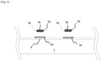
- a vehicle glass assembly 1 comprises a glass substrate layer 2, an optional coloured ceramic band 6 sintered on a peripheral portion of the glass substrate layer 2, an electrically conductive layer 3 which comprises a connecting terminal 3a and an electrically conductive wire pattern 3b sintered on the glass substrate layer 2 and/or on the coloured ceramic band 6, a lead-free solder layer 4 on the conductive layer 3, and a harness 5 which comprises a connector 5a made of a metal plate, metal wire 5b such as copper wire, and an envelope or sheath 5c covering the metal wire.
- a solder connection is formed between the connector 5a and the electrically conductive layer 3 via the lead-free solder layer 4.
- Figs. 3 and 4 relate to steps (A), (B) and (C), and details are described
- the vehicle glass assembly 1 is produced by a production method comprising:
- the amount of lead-free solder is smaller than 4.5 mg, it becomes difficult to achieve enough soldered area at the connecting terminal 3a, resulting in a weaker solder connection.
- the amount is larger than 13 mg, the compensation of mechanical stresses between the glass substrate layer 2 and the connector 5a may be inadequate, resulting in the occurrence of cracks in the glass substrate layer 2, the conductive layer 3, and/or in the coloured ceramic band 6.
- the amount may typically be between 4.5 mg and 11 mg, preferably between 4.5 mg and 10 mg.
- the vehicle glass assembly 1 comes to comprise solder connection in which all lead-free solder is disposed between the flat portions 5d and the connecting terminal 3a. Further, the vehicle glass assembly 1 may comprise solder connection in which all lead-free solders recess from all edges of the flat portion 5d, in order that the lead-free solder is certainly not spilled out from the space.
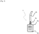
- Fig. 3 is a schematic view showing a harness in the state after step (A).
- the block 4p made of lead-free solder is soldered onto the flat portion 5d of the connector 5a.
- the flat portion 5d is made of metal plate; preferably in general the entire connector may be made of a single metal plate.
- the connector 5a is disposed at the terminal of the metal wire 5b, and the metal wire 5b is connected to at least the flat portion 5d.
- the metal wire 5b may be crimped with the connector 5a that is preferably a B-crimp.
- the metal wire 5b - which in practice may be a bundle of plural wires - is typically covered with the envelope or sheath 5c which may be made of e.g. PVC, PE, rubber material, fluororesin or the like. It is generally to be connected to apparatus such as an amplifier, audio equipment, radio equipment, a television, a navigation system, or the like.
- the area of the flat portion 5d may typically be between 10 mm 2 and 15 mm 2 . If the area is smaller than 10 mm 2 the solder connection may become weak. On the other hand, the more the area is larger than about 15 mm 2 , the more mechanical stress tend to be transferred to the glass substrate layer 2 (due to brittleness of the lead-free solder and differential thermal expansion coefficients among the glass substrate layer 2, the lead-free solder layer 4 and the connector 3a). In the light of these factors, the area may desirably be between 10 mm 2 and 15 mm 2 , more preferably between 11 mm 2 and 14 mm 2
- the thickness of the metal plate may also affect the melting process of the block 4p in step (C).
- the thicker the metal plate the more heating energy is required when the melting process is carried out and this may lead to more mechanical stress in the solder connection.
- the less thick the metal plate the more difficult the connector 3a is for handling and manufacture.
- the thickness of the metal plate may preferably be between 0.2 mm and 0.4 mm, more preferably between 0.25 mm and 0.35 mm, still more preferably about 0.3 mm.
- the shape of the flat portion 5d may be a rectangle, a square, oval or circle etc.
- the material of the metal plate there can be mentioned Cu or Cu alloy, Fe alloy comprising Ni or Cr such as INVAR 48 (FeNi48, consisting of 48% nickel in iron alloy). Among these materials, Fe alloy is preferable, and INVAR 48 is the most preferable.
- step (A) the lead-free solder is soldered onto the flat connector portion 5d to form the block 4p.
- the volume of the block 4p may typically be between 0.6 mm 3 and 1.4 mm 3 . If the volume is smaller than 0.6 mm 3 , the solder connection may sometimes become weak. On the other hand, if the volume is larger than 1.4 mm 3 , the compensation of mechanical stresses between the glass substrate layer 2 and the connector 5a may sometimes be inadequate, resulting in the occurrence of cracks in the glass substrate layer 2, the conductive layer 3, and/or in the coloured ceramic band 6.
- the thickness of the block 4p may also affect the quality of the lead-free solder layer 4. If there is a limited amount of the lead-free solder, an inappropriate thickness of the block 4p may result in an inhomogeneous layer 4 with porosity which may cause mechanical stress in the glass substrate layer 2. Considering these factors, the thickness may typically be between 0.2 mm and 0.4 mm, preferably between 0.2 mm and 0.35 mm.
- the lead-free solder contains tin as a major component.
- lead-free solder there can be mentioned Sn-Ag based solder, Sn-Ag-Cu based solder and the like.
- the content of Sn may be e.g. 95 mass% to 99 mass%, preferably 96 mass% to 98 mass%.
- the content of Ag may be e.g. 1 mass% to 5 mass%, preferably 2 mass% to 4 mass%.
- the content of Cu may be e.g. 0 mass% to 1.5 mass%, preferably 0.1 mass% to 1 mass%.
- Fig. 4 is a cross-sectional view showing the harness and a glass substrate layer before step (C); the cross-sectional view is at X-Y of Fig. 1 .
- the glass substrate layer 2 comprising the conductive layer 3 is provided.
- the glass substrate layer optionally comprises the coloured ceramic band 6 between the glass substrate layer 2 and the conductive layer 3.
- the glass substrate layer 2 preferably has a curved shape, obtainable e.g. by a known process of bending a flat glass sheet.
- the glass substrate layer 2 may be a non-tempered glass, a thermally tempered glass, a chemically tempered glass or a laminated glass. In the laminated glass, the two glasses are preferably non-tempered glasses.
- the glass substrate layer 2 is a laminated glass comprising two or more non-tempered glasses (i.e. all glasses are non-tempered glasses) and the conductive layer 3 is a hot printed wire.
- soda-lime silicate glass as defined by ISO16293-1 can be used as the material of the glass substrate layer 2.
- the soda-lime silicate glass may comprise a colorant such as iron oxide and cobalt oxide, whereby to present a colour such as pale green, dark green, pale gray, dark gray, pale blue or dark blue.
- the coloured ceramic band 6 is of a coloured ceramic composition preferably comprising an inorganic heat-resisting pigment and a glass frit that has a lower softening temperature than that of the glass substrate layer 2.
- a peripheral band is well-known, and is sometimes called a frit layer, ceramic band or paint band.
- the coloured ceramic band 6 is used to overlie an adhesion area between the vehicle glass assembly 1 and a body flange of a vehicle. It can improve weather resistance of the adhesion area and/or make it invisible by covering it, so that black is preferable as the colour of the coloured ceramic band layer 6.
- the thickness of the coloured ceramic band may be e.g. 5 ⁇ m to 25 ⁇ m, preferably 5 ⁇ m to 15 ⁇ m.
- the coloured ceramic band 6 can be obtained for example by the following process. That is, a ceramic paste comprising the inorganic heat-resisting pigment, a glass frit and organic solvent is applied on the peripheral portion of the glass substrate layer 2 by a screen printing method or the like, and then heated, thereby volatilizing the organic solvent. Subsequently, the composition comprising the inorganic heat-resisting pigment and glass frit is sintered on the glass substrate layer thereby forming the coloured ceramic band 6.
- the inorganic heat-resisting pigment is mixed in the colour ceramic to give a desired color.
- the grain diameter of the inorganic heat-resisting pigment may be e.g. 0.1 ⁇ m to 10 ⁇ m, preferably 0.2 ⁇ m to 5 ⁇ m, expressed as a D50 value.
- the inorganic heat-resisting pigment known ones can be used.
- black pigments there can be mentioned copper-chromium complex oxide, iron-manganese complex oxide, cobalt-iron-manganese complex oxide, copper-chromium-manganese complex oxide, magnetite and the like.
- blue pigment there can be mentioned cobalt blue, chromium green, cobalt-zinc-nickel-titanium complex oxide, cobalt-aluminum-chromium complex oxide and the like.
- white pigment e.g. titanium white, zinc oxide and the like
- red pigment e.g. rouge and the like
- yellow pigment e.g. titanium yellow, titanium-barium-nickel complex oxide, titanium-antimony-nickel complex oxide, titanium-antimony-chromium complex oxide and the like
- other pigments in line with the skilled person's knowledge.
- the glass frit is fused through a heating process to form the coloured ceramic band 6.
- the glass frit usual ones can be used.
- the glass frit there can be mentioned borosilicate glass, boron-zinc-silicate glass, bismuth-based glass and the like.
- a softening temperature of the glass frit may be a lower temperature, for example, 300-600°C, preferably 350-580°C, than a bending and forming temperature of the glass substrate layer 2.
- the grain diameter of the glass frit may be 0.1 ⁇ m to 10 ⁇ m, preferably 0.2 ⁇ m to 5 ⁇ m, further preferably 1 ⁇ m to 4 ⁇ m (determined as D50).
- the content of the glass material made of the glass frit may be 60 mass% to 80 mass%.
- the coloured ceramic band 6 can be also obtained through other methods besides the above-mentioned process.
- Such other processes there can be mentioned a digital printing process.
- the conductive layer 3, preferably sintered on the glass substrate layer 2 and/or on the coloured ceramic band 6, comprises the electrically conductive wire pattern 3b and the connecting terminal 3a.
- the conductive layer 3 preferably comprises silver metal (silver or silver alloy) and a glass frit which may be selected from those exemplified above.
- the thickness of the electrically conductive layer 3 may be e.g. 3 ⁇ m to 20 ⁇ m, preferably 5 ⁇ m to 15 ⁇ m, more preferably 12 ⁇ m to 17 ⁇ m.
- the conductive layer 3 can be obtained through the following process. That is, a silver paste comprising the silver metal, the glass frit and an organic solvent is applied on the glass substrate layer 2, or on coated and dried ceramic colour paste by screen printing method and the like, and then is heated, thereby volatilizing the organic solvent. Subsequently, the composition comprising the silver metal and the glass frit is sintered on the glass substrate layer 2 or coloured ceramic band 6, thereby forming the electrically conductive layer 3. As is well-known, the conductive layer 3 can be used as a printed hot-wire such as a defogger and defroster, or as an antenna.
- the grain diameter of the silver metal may be e.g. 0.1 ⁇ m to 10 ⁇ m, preferably 0.2 ⁇ m to 7 ⁇ m (determined as D50).
- the content of the silver metal may be e.g. 65 mass% to 99 mass%, preferably 75 mass% to 98 mass%.
- the conductive layer 3 can be also obtained by other methods besides the above-mentioned process. As an example of such other processes, there can be mentioned a digital printing process.
- step (C) the desired vehicle glass assembly 1 is obtained.
- step (C) the block 4p is sandwiched between the flat portion 5d and the connecting terminal 3a, and then the block 4p is melted and may be pressed therebetween to form a solder connection between the connector 5a and the connecting terminal 3a, forming the lead-free solder layer 4.
- the lead-free solver layer 4 may be thinner than the block 4p in thickness.
- the block 4p may be heated up from a melting temperature of the lead-free solder to 50°C above the melting temperature.
- the reflow process may be carried out using a soldering iron or electrical heating of the connector 5a. It is preferable that the reflow process is carried out through the electrical heating of the connector 5a.
- the thickness of the lead-free solder layer 4 is desirably between 0.1 mm and 0.3 mm. If the thickness is more than 0.3 mm, a difference of thermal expansion behavior between the glass substrate layer 2 and the solder layer 4 may cause mechanical stress at an interface of the glass substrate layer 2 or the electrically conductive layer 3 during the melting process, or while using the window glass 1 fitted in a vehicle. The mechanical stress may enhance a risk of permanent tensile stress in the glass substrate layer 2, resulting in crack generation in the glass substrate layer 2. On the other hand, if the thickness is less than 0.1 mm it may enhance a risk of a generation of hot spots at the solder layer during the reflow process. The generation of hot spots may result in a residual stress in the glass substrate layer 2, which then causes cracking in the glass substrate layer 2.
- the thickness of the lead-free solder layer 4 is preferably between 0.15 mm and 0.25 mm.
- a base test specimen was provided.
- the specimen comprises a non-tempered glass substrate layer 2 with 3 mm thickness and made of a soda-lime silicate glass defined by ISO16293-1, and a conductive layer 3 comprising an electrically conductive wire pattern 3b and a connecting terminal 3a as shown in Figures 1 , 2 and 4 .
- the shape and area of the connecting terminal 3a was, respectively, a rectangle and 15 mm 2 . This corresponds to step (B) of the method.
- a harness 5 comprising a connector 5a, metal (copper) wire 5b and a PVC sheath 5c covering the wire 5b was provided as shown in Figures 1 to 4 .
- the connector 5a was made of Invar 48 (FeNi48 alloy) metal plate with 0.3 mm thickness, and was a B-crimp clamping the metal wire 5b.
- the connector 5a had a flat portion 5d of rectangular shape and 11.25 mm 2 area.
- a lead-free solder made of Sn (96.5 mass%)-Ag (3.0 mass%)-Cu (0.5 mass%) was soldered onto the flat portion 5d to form block 4p.
- the 4p on the flat portion 5d was away from all edges of the flat portions 5d.
- the soldered amount was 7.5 mg, and the volume and thickness of the block 4p were respectively 1.012 mm 3 and 0.2 mm. This corresponds to step (A) of the method.
- the block 4p was placed on the connecting terminal 3a so as to be sandwiched between the flat portion 5d and the connecting terminal 3a.
- the connecting terminal 3a was electrically heated so that block 4p is melted to form a solder connection between the connector and the connecting terminal. This corresponds to step (C) of the method.
- step (C) the lead-free solder did not spill out a space between the flat portions 5d and the connecting terminal 3a.
- the soldered specimen was taken to be the vehicle glass assembly 1.
- Example 1 The procedure of Example 1 was repeated with the exception that the amount of lead-free solder was 8.8 mg, and the volume and thickness of the block 4p were respectively 1.196 mm 3 and 0.2 mm. No cracks were observed in the glass substrate layer 2 for any of the samples in the heat cycle tests.
- Example 1 The procedure of Example 1 was repeated with the exception that the amount of lead-free solder was 4.8 mg, and the volume and thickness of the block 4p were respectively 0.65 mm 3 and 0.2 mm. No cracks were observed in the glass substrate layer 2 for any of the samples in the heat cycle tests.
- Example 1 The procedure of Example 1 was repeated with the exception that the amount of lead-free solder was 32.5 mg, and the volume and thickness of the block 4p were respectively 4.4 mm 3 and 0.5 mm. In the heat cycle tests cracking was observed for 7 out of 10 samples in this comparative example.
- Example 1 The procedure of Example 1 was repeated with the exception that the amount of lead-free solder was 14 mg, and the volume and thickness of the block 4p were respectively 1.9 mm 3 and 0.2 mm. Cracking was observed for 4 out of 10 of samples in this comparative example.
Landscapes
- Engineering & Computer Science (AREA)
- Mechanical Engineering (AREA)
- Chemical & Material Sciences (AREA)
- Materials Engineering (AREA)
- Metallurgy (AREA)
- Organic Chemistry (AREA)
- Manufacturing & Machinery (AREA)
- Composite Materials (AREA)
- Connections Effected By Soldering, Adhesion, Or Permanent Deformation (AREA)
- Glass Compositions (AREA)
Claims (15)
- Verfahren zur Herstellung einer Fahrzeugglasanordnung, umfassend:(A) Bereitstellen eines Kabelbaums (5), der Folgendes umfasst:einen Metalldraht (5b),einen Verbinder (5a) an einem Anschlusspunkt des Metalldrahts (5b), umfassend einen flachen Abschnitt (5d), der aus einer Metallplatte besteht, undeinen Block (4p) aus bleifreiem Lötmittel, das Zinn als Hauptkomponente enthält, der auf dem flachen Abschnitt (5d) des Verbinders (5a) angelötet ist;(B) Bereitstellen einer Glassubstratschicht (2), über der eine leitfähige Schicht (3), umfassend ein elektrisch leitfähiges Drahtmuster (3b) und einen Verbindungsanschluss (3a), ausgebildet ist;(C) sandwichartiges Anordnen des Blocks (4p) zwischen dem flachen Abschnitt (5d) des Verbinders und des Verbindungsanschlusses (3a) der leitfähigen Schicht (3) und dann Schmelzen des Blocks, um eine bleifreie Lötmittelschicht (4) als eine Lötverbindung zwischen dem Verbinder (5a) und dem Verbindungsanschluss (3a) auszubilden;wobeidie Menge des bleifreien Lötmittels zwischen 4,5 mg und 13 mg beträgt,der Lötblock (4p) auf dem flachen Abschnitt (5d) von allen Rändern des flachen Abschnitts (5d) beabstandet ist unddas gesamte bleifreie Lötmittel der Lötschicht (4) in der Lötverbindung zwischen dem flachen Abschnitt (5d) und dem Verbindungsanschluss (3a) angeordnet ist.
- Herstellungsverfahren nach Anspruch 1, wobei die Menge des bleifreien Lötmittels zwischen 4,5 mg und 10 mg beträgt.
- Herstellungsverfahren nach Anspruch 1 oder 2, wobei die Fläche des flachen Abschnitts (5d) zwischen 10 mm2 und 15 mm2 beträgt.
- Herstellungsverfahren nach Anspruch 1, 2 oder 3, wobei die Dicke der Metallplatte zwischen 0,2 mm und 0,4 mm beträgt.
- Herstellungsverfahren nach einem der Ansprüche 1 bis 4, wobei der Verbinder (5a) ein B-Crimp ist, der an den Metalldraht (5b) geklemmt ist.
- Herstellungsverfahren nach einem der Ansprüche 1 bis 5, wobei das Volumen des Blocks (4p) zwischen 0,6 mm3 und 1,4 mm3 beträgt.
- Herstellungsverfahren nach einem der Ansprüche 1 bis 6, wobei die Dicke des Blocks (4p) zwischen 0,2 mm und 0,4 mm beträgt.
- Herstellungsverfahren nach einem der Ansprüche 1 bis 7, wobei die leitfähige Schicht (3) ein gedruckter Hitzdraht ist und die Glassubstratschicht (2) aus nichtgetempertem Glas besteht.
- Herstellungsverfahren nach einem der Ansprüche 1 bis 8, wobei das gesamte bleifreie Lötmittel in der Lötverbindung von allen Rändern des flachen Abschnitts (5d) vertieft ist.
- Herstellungsverfahren nach einem der Ansprüche 1 bis 9, wobei die Metallplatte aus Cu, einer Cu-Legierung oder einer Fe-Legierung, umfassend Ni oder Cr, besteht.
- Herstellungsverfahren nach einem der Ansprüche 1 bis 10, wobei das bleifreie Lötmittel ein Lötmittel auf Sn-Ag-Basis oder ein Lötmittel auf Sn-Ag-Cu-Basis ist.
- Herstellungsverfahren nach Anspruch 11, wobei das bleifreie Lötmittel 95 bis 99 Massen-% Sn, 1 bis 5 Massen-% Ag und 0 bis 1,5 Massen-% Cu besteht.
- Herstellungsverfahren nach einem der Ansprüche 1 bis 12, wobei die bleifreie Lötschicht (4) dünner ist als der Block (4p).
- Herstellungsverfahren nach einem der Ansprüche 1 bis 13, wobei der Block (4p) in Schritt (C) unter Verwendung eines Löteisens oder durch elektrisches Erhitzen des Verbinders (5a) geschmolzen wird.
- Herstellungsverfahren nach einem der Ansprüche 1 bis 14, wobei die bleifreie Lötmittelschicht (4) in der Lötverbindung eine Dicke zwischen 0,1 mm und 0,3 mm aufweist.
Applications Claiming Priority (2)
| Application Number | Priority Date | Filing Date | Title |
|---|---|---|---|
| GBGB1804622.7A GB201804622D0 (en) | 2018-03-22 | 2018-03-22 | Method of producing a vehicle glass assembly |
| PCT/JP2019/007427 WO2019181395A1 (en) | 2018-03-22 | 2019-02-27 | Method of producing a vehicle glass assembly |
Publications (2)
| Publication Number | Publication Date |
|---|---|
| EP3768465A1 EP3768465A1 (de) | 2021-01-27 |
| EP3768465B1 true EP3768465B1 (de) | 2024-10-16 |
Family
ID=62067931
Family Applications (1)
| Application Number | Title | Priority Date | Filing Date |
|---|---|---|---|
| EP19712053.8A Active EP3768465B1 (de) | 2018-03-22 | 2019-02-27 | Verfahren zur herstellung eines fahrzeugbauteils aus glas |
Country Status (6)
| Country | Link |
|---|---|
| US (1) | US12128493B2 (de) |
| EP (1) | EP3768465B1 (de) |
| JP (1) | JP7289846B2 (de) |
| CN (1) | CN111886108B (de) |
| GB (1) | GB201804622D0 (de) |
| WO (1) | WO2019181395A1 (de) |
Families Citing this family (2)
| Publication number | Priority date | Publication date | Assignee | Title |
|---|---|---|---|---|
| GB201804622D0 (en) * | 2018-03-22 | 2018-05-09 | Central Glass Co Ltd | Method of producing a vehicle glass assembly |
| GB201804624D0 (en) * | 2018-03-22 | 2018-05-09 | Central Glass Co Ltd | Method of producing a vehicle glass assembly |
Family Cites Families (63)
| Publication number | Priority date | Publication date | Assignee | Title |
|---|---|---|---|---|
| US2644066A (en) * | 1951-07-05 | 1953-06-30 | Blue Ridge Glass Corp | Electrical connector for resistance elements on glass plates |
| LU34357A1 (de) * | 1955-05-11 | |||
| US3813519A (en) * | 1964-11-09 | 1974-05-28 | Saint Gobain | Electrically heated glass window |
| FR2509947A1 (fr) * | 1981-07-15 | 1983-01-21 | Saint Gobain Vitrage | Vitrage chauffant electrique |
| US4634041A (en) * | 1984-06-29 | 1987-01-06 | International Business Machines Corporation | Process for bonding current carrying elements to a substrate in an electronic system, and structures thereof |
| JPS63302594A (ja) * | 1987-06-03 | 1988-12-09 | Hitachi Ltd | 厚膜導体電極の形成方法 |
| US4877176A (en) * | 1987-11-25 | 1989-10-31 | Northern Telecom Limited | Soldering pins into printed circuit boards |
| US5110761A (en) * | 1988-09-09 | 1992-05-05 | Motorola, Inc. | Formed top contact for non-flat semiconductor devices |
| US5011066A (en) * | 1990-07-27 | 1991-04-30 | Motorola, Inc. | Enhanced collapse solder interconnection |
| US5172852A (en) * | 1992-05-01 | 1992-12-22 | Motorola, Inc. | Soldering method |
| DE9310699U1 (de) * | 1993-07-17 | 1993-09-02 | Richard Hirschmann Gmbh & Co, 73728 Esslingen | Kontaktelement |
| DE4439645C1 (de) * | 1994-11-07 | 1996-04-11 | Sekurit Saint Gobain Deutsch | Stromanschlußelement für eine heizbare Autoglasscheibe |
| US5879206A (en) * | 1997-11-05 | 1999-03-09 | Ford Global Technologies, Inc. | Terminal connector capable of attachment to a metallic surface |
| DE19750073A1 (de) * | 1997-11-12 | 1999-05-20 | Bosch Gmbh Robert | Schaltungsträgerplatte |
| US6316736B1 (en) * | 1998-06-08 | 2001-11-13 | Visteon Global Technologies, Inc. | Anti-bridging solder ball collection zones |
| US6169253B1 (en) * | 1998-06-08 | 2001-01-02 | Visteon Global Technologies, Inc. | Solder resist window configurations for solder paste overprinting |
| US6406636B1 (en) * | 1999-06-02 | 2002-06-18 | Megasense, Inc. | Methods for wafer to wafer bonding using microstructures |
| DE10002777C1 (de) * | 2000-01-22 | 2001-08-09 | Saint Gobain Sekurit D Gmbh | Kontaktierung einer Scheibe mit elektrischen Funktionen |
| CN1177512C (zh) | 2000-01-25 | 2004-11-24 | 意大利维特洛公司 | 带电路的窗用玻璃及其制造方法 |
| US6730848B1 (en) * | 2001-06-29 | 2004-05-04 | Antaya Technologies Corporation | Techniques for connecting a lead to a conductor |
| US6961505B2 (en) * | 2001-12-25 | 2005-11-01 | Yamaha Corporation | Metal holder, optical component composite body and manufacturing method |
| JP2004189023A (ja) * | 2002-12-09 | 2004-07-08 | Asahi Glass Co Ltd | 自動車用窓ガラスの端子及びその取付け方法 |
| US7159756B2 (en) * | 2003-08-29 | 2007-01-09 | Ppg Industries Ohio, Inc. | Method of soldering and solder compositions |
| US7416106B1 (en) * | 2003-09-29 | 2008-08-26 | Emc Corporation | Techniques for creating optimized pad geometries for soldering |
| JP4502690B2 (ja) * | 2004-04-13 | 2010-07-14 | 富士通株式会社 | 実装基板 |
| US7658001B1 (en) * | 2005-04-14 | 2010-02-09 | Hutchinson Technology Incorporated | Electrical connector for disk drive suspension assembly and method of non-contact solder attachment of same |
| DE102006017675A1 (de) * | 2006-04-12 | 2007-10-18 | Pilkington Automotive Deutschland Gmbh | Glasscheibe mit elektrischem Funktionselement mit durch Lötverbindung befestigten Anschlußdrähten und Verfahren zum Herstellen elektrischer Anschlüsse |
| DE102007059818B3 (de) * | 2007-12-11 | 2009-04-09 | Saint-Gobain Sekurit Deutschland Gmbh & Co. Kg | Fensterscheibe mit einem elektrischen Flachanschlusselement |
| TWI341224B (en) * | 2008-04-03 | 2011-05-01 | Chimei Innolux Corp | Solder bonding structure and solder bonding method thereof |
| DE102009006856A1 (de) | 2009-01-30 | 2010-08-19 | Saint-Gobain Sekurit Deutschland Gmbh & Co. Kg | Scheibe mit mindestens einem integrierten Leuchtfeld |
| US8210422B2 (en) * | 2009-09-30 | 2012-07-03 | Apple Inc. | Solder containment brackets |
| EP2367399A1 (de) | 2010-03-02 | 2011-09-21 | Saint-Gobain Glass France | Scheibe mit einem elektrischen Anschlusselement |
| EP2408260A1 (de) * | 2010-07-13 | 2012-01-18 | Saint-Gobain Glass France | Glasscheibe mit einem elektrischen Anschlusselement |
| JP5886419B2 (ja) * | 2011-05-10 | 2016-03-16 | サン−ゴバン グラス フランスSaint−Gobain Glass France | 電気的な接続素子を備えているガラス板 |
| PL3751960T3 (pl) * | 2011-05-10 | 2022-06-27 | Saint-Gobain Glass France | Szyba z elektrycznym elementem przyłączeniowym |
| TWI558039B (zh) * | 2012-06-06 | 2016-11-11 | 法國聖戈本玻璃公司 | 帶有電連接元件之板、製造彼之方法、及彼之用途 |
| US9837727B2 (en) | 2012-09-14 | 2017-12-05 | Saint-Gobain Glass France | Pane having an electrical connection element |
| MX346392B (es) * | 2012-09-14 | 2017-03-16 | Saint Gobain | Cristal con un elemento de conexión eléctrica. |
| MX344768B (es) * | 2012-11-21 | 2017-01-06 | Saint Gobain | Cristal con elemento de conexion electrica y placas compensadoras. |
| WO2015023921A1 (en) * | 2013-08-16 | 2015-02-19 | Agc Automotive Americas R&D, Inc. | Window assembly with casing for solder joint |
| FR3017332B1 (fr) | 2014-02-10 | 2016-02-19 | Saint Gobain | Vitrage lumineux avec isolateur optique. |
| US9536851B2 (en) | 2014-09-05 | 2017-01-03 | Infineon Technologies Ag | Preform structure for soldering a semiconductor chip arrangement, a method for forming a preform structure for a semiconductor chip arrangement, and a method for soldering a semiconductor chip arrangement |
| ES2811953T3 (es) * | 2014-10-03 | 2021-03-15 | Nippon Steel Corp | Pieza estampada en caliente que tiene una junta soldada y método de fabricación para la pieza estampada en caliente |
| EP3235340B1 (de) * | 2014-12-16 | 2020-07-15 | Saint-Gobain Glass France | Scheibe mit einem elektrischen anschlusselement und einem flexiblen anschlusskabel |
| DE102015107309A1 (de) * | 2015-05-11 | 2016-11-17 | Newfrey Llc | Fügebauteil und Fügeverfahren |
| JP6725971B2 (ja) * | 2015-07-14 | 2020-07-22 | 日本板硝子株式会社 | ガラス板モジュール |
| KR102087075B1 (ko) * | 2016-05-10 | 2020-03-11 | 쌩-고벵 글래스 프랑스 | 납땜 인두용 납땜 선단부 |
| FR3054403B1 (fr) * | 2016-07-22 | 2019-10-18 | Saint-Gobain Glass France | Vitrage avec element electriquement conducteur et sa connexion electrique |
| FR3054771B1 (fr) * | 2016-07-27 | 2020-11-06 | Saint Gobain | Vitrage muni d'un dispositif conducteur electrique avec zones de soudure ameliorees |
| WO2018158574A1 (en) * | 2017-03-02 | 2018-09-07 | Pilkington Group Limited | Window assembly having a terminal connector |
| CN109500510A (zh) * | 2017-09-14 | 2019-03-22 | 株式会社田村制作所 | 无铅软钎料合金、电子电路基板和电子控制装置 |
| CN111226499B (zh) * | 2017-10-23 | 2022-11-18 | 伊利诺斯工具制品有限公司 | 用于印制导体的高瓦数无焊柔性连接器 |
| WO2019092947A1 (ja) * | 2017-11-07 | 2019-05-16 | セントラル硝子株式会社 | 車両窓用ガラスアッセンブリー |
| KR102480461B1 (ko) * | 2017-11-30 | 2022-12-21 | 쌩-고벵 글래스 프랑스 | 차량용 창유리의 터미널 솔더링 장치 및 방법 |
| GB201804624D0 (en) * | 2018-03-22 | 2018-05-09 | Central Glass Co Ltd | Method of producing a vehicle glass assembly |
| GB201804622D0 (en) * | 2018-03-22 | 2018-05-09 | Central Glass Co Ltd | Method of producing a vehicle glass assembly |
| US11246189B2 (en) * | 2018-05-21 | 2022-02-08 | Magna Mirrors Of America, Inc. | Vehicular window assembly with magnetic connector |
| WO2019235266A1 (ja) * | 2018-06-05 | 2019-12-12 | Agc株式会社 | 端子付き車両用窓ガラス |
| WO2020050120A1 (ja) * | 2018-09-07 | 2020-03-12 | セントラル硝子株式会社 | 車両窓用ガラスアッセンブリー |
| US20220045467A1 (en) * | 2018-12-12 | 2022-02-10 | Connlaoth MulHolland | Soldering Block for LED Tape Light |
| CN109648222A (zh) * | 2019-01-21 | 2019-04-19 | 上海莜玮汽车零部件有限公司 | 一种无铅焊料合金及其应用 |
| WO2022039020A1 (ja) * | 2020-08-19 | 2022-02-24 | Agc株式会社 | 車両用窓ガラス |
| US20230084191A1 (en) * | 2021-09-16 | 2023-03-16 | Magna Mirrors Of America, Inc. | Vehicular rear slider window assembly with electrical connection to movable panel heater grid |
-
2018
- 2018-03-22 GB GBGB1804622.7A patent/GB201804622D0/en not_active Ceased
-
2019
- 2019-02-27 US US16/981,777 patent/US12128493B2/en active Active
- 2019-02-27 JP JP2020548838A patent/JP7289846B2/ja active Active
- 2019-02-27 CN CN201980020827.XA patent/CN111886108B/zh active Active
- 2019-02-27 EP EP19712053.8A patent/EP3768465B1/de active Active
- 2019-02-27 WO PCT/JP2019/007427 patent/WO2019181395A1/en not_active Ceased
Also Published As
| Publication number | Publication date |
|---|---|
| US20210121968A1 (en) | 2021-04-29 |
| JP2021517715A (ja) | 2021-07-26 |
| CN111886108B (zh) | 2022-02-08 |
| US12128493B2 (en) | 2024-10-29 |
| EP3768465A1 (de) | 2021-01-27 |
| WO2019181395A1 (en) | 2019-09-26 |
| GB201804622D0 (en) | 2018-05-09 |
| CN111886108A (zh) | 2020-11-03 |
| JP7289846B2 (ja) | 2023-06-12 |
Similar Documents
| Publication | Publication Date | Title |
|---|---|---|
| US12144071B2 (en) | Vehicle window glass with electrical connector soldered by lead-free solder | |
| US10297929B2 (en) | Pane having an electrical connection element | |
| EP2664503B1 (de) | Verfahren zur herstellung von einer fensterscheibe für fahrzeuge | |
| CN104620673A (zh) | 具有电连接元件的窗玻璃 | |
| US20190174582A1 (en) | Glazing equipped with an electrically conductive device with improved soldering zones | |
| EP3768465B1 (de) | Verfahren zur herstellung eines fahrzeugbauteils aus glas | |
| US10512169B2 (en) | Glazing equipped with an electrically conductive device possessing an improved resistance to temperature cycling tests | |
| EP3768464B1 (de) | Verfahren zur herstellung eines fahrzeugbauteils aus glas | |
| US20210315061A1 (en) | Vehicle window glass assembly | |
| US20210184374A1 (en) | Electrical crimp connector with a tail | |
| WO2025254638A1 (en) | A pane for a vehicle having a connection element comprising a solder material layer | |
| TR2024007152A1 (tr) | Bi̇r bağlanti elemanina sahi̇p bi̇r araç i̇çi̇n bi̇r panel |
Legal Events
| Date | Code | Title | Description |
|---|---|---|---|
| STAA | Information on the status of an ep patent application or granted ep patent |
Free format text: STATUS: UNKNOWN |
|
| STAA | Information on the status of an ep patent application or granted ep patent |
Free format text: STATUS: THE INTERNATIONAL PUBLICATION HAS BEEN MADE |
|
| PUAI | Public reference made under article 153(3) epc to a published international application that has entered the european phase |
Free format text: ORIGINAL CODE: 0009012 |
|
| STAA | Information on the status of an ep patent application or granted ep patent |
Free format text: STATUS: REQUEST FOR EXAMINATION WAS MADE |
|
| 17P | Request for examination filed |
Effective date: 20201021 |
|
| AK | Designated contracting states |
Kind code of ref document: A1 Designated state(s): AL AT BE BG CH CY CZ DE DK EE ES FI FR GB GR HR HU IE IS IT LI LT LU LV MC MK MT NL NO PL PT RO RS SE SI SK SM TR |
|
| AX | Request for extension of the european patent |
Extension state: BA ME |
|
| DAV | Request for validation of the european patent (deleted) | ||
| DAX | Request for extension of the european patent (deleted) | ||
| REG | Reference to a national code |
Ref country code: DE Ref legal event code: R079 Free format text: PREVIOUS MAIN CLASS: B23K0035260000 Ipc: H01Q0001120000 Ref document number: 602019060439 Country of ref document: DE |
|
| GRAP | Despatch of communication of intention to grant a patent |
Free format text: ORIGINAL CODE: EPIDOSNIGR1 |
|
| STAA | Information on the status of an ep patent application or granted ep patent |
Free format text: STATUS: GRANT OF PATENT IS INTENDED |
|
| RIC1 | Information provided on ipc code assigned before grant |
Ipc: H01R 4/02 20060101ALI20240425BHEP Ipc: C22C 13/00 20060101ALI20240425BHEP Ipc: B23K 35/26 20060101ALI20240425BHEP Ipc: H01R 12/57 20110101ALI20240425BHEP Ipc: C22C 19/03 20060101ALI20240425BHEP Ipc: B23K 35/30 20060101ALI20240425BHEP Ipc: B23K 35/02 20060101ALI20240425BHEP Ipc: B22F 7/08 20060101ALI20240425BHEP Ipc: H05B 3/84 20060101ALI20240425BHEP Ipc: H01Q 1/12 20060101AFI20240425BHEP |
|
| INTG | Intention to grant announced |
Effective date: 20240515 |
|
| GRAS | Grant fee paid |
Free format text: ORIGINAL CODE: EPIDOSNIGR3 |
|
| GRAA | (expected) grant |
Free format text: ORIGINAL CODE: 0009210 |
|
| STAA | Information on the status of an ep patent application or granted ep patent |
Free format text: STATUS: THE PATENT HAS BEEN GRANTED |
|
| AK | Designated contracting states |
Kind code of ref document: B1 Designated state(s): AL AT BE BG CH CY CZ DE DK EE ES FI FR GB GR HR HU IE IS IT LI LT LU LV MC MK MT NL NO PL PT RO RS SE SI SK SM TR |
|
| REG | Reference to a national code |
Ref country code: GB Ref legal event code: FG4D |
|
| REG | Reference to a national code |
Ref country code: CH Ref legal event code: EP |
|
| REG | Reference to a national code |
Ref country code: IE Ref legal event code: FG4D |
|
| REG | Reference to a national code |
Ref country code: DE Ref legal event code: R096 Ref document number: 602019060439 Country of ref document: DE |
|
| REG | Reference to a national code |
Ref country code: LT Ref legal event code: MG9D |
|
| REG | Reference to a national code |
Ref country code: NL Ref legal event code: MP Effective date: 20241016 |
|
| REG | Reference to a national code |
Ref country code: AT Ref legal event code: MK05 Ref document number: 1733709 Country of ref document: AT Kind code of ref document: T Effective date: 20241016 |
|
| PG25 | Lapsed in a contracting state [announced via postgrant information from national office to epo] |
Ref country code: NL Free format text: LAPSE BECAUSE OF FAILURE TO SUBMIT A TRANSLATION OF THE DESCRIPTION OR TO PAY THE FEE WITHIN THE PRESCRIBED TIME-LIMIT Effective date: 20241016 |
|
| PGFP | Annual fee paid to national office [announced via postgrant information from national office to epo] |
Ref country code: LU Payment date: 20250227 Year of fee payment: 7 |
|
| PG25 | Lapsed in a contracting state [announced via postgrant information from national office to epo] |
Ref country code: NL Free format text: LAPSE BECAUSE OF FAILURE TO SUBMIT A TRANSLATION OF THE DESCRIPTION OR TO PAY THE FEE WITHIN THE PRESCRIBED TIME-LIMIT Effective date: 20241016 |
|
| PG25 | Lapsed in a contracting state [announced via postgrant information from national office to epo] |
Ref country code: HR Free format text: LAPSE BECAUSE OF FAILURE TO SUBMIT A TRANSLATION OF THE DESCRIPTION OR TO PAY THE FEE WITHIN THE PRESCRIBED TIME-LIMIT Effective date: 20241016 Ref country code: PT Free format text: LAPSE BECAUSE OF FAILURE TO SUBMIT A TRANSLATION OF THE DESCRIPTION OR TO PAY THE FEE WITHIN THE PRESCRIBED TIME-LIMIT Effective date: 20250217 Ref country code: IS Free format text: LAPSE BECAUSE OF FAILURE TO SUBMIT A TRANSLATION OF THE DESCRIPTION OR TO PAY THE FEE WITHIN THE PRESCRIBED TIME-LIMIT Effective date: 20250216 |
|
| PGFP | Annual fee paid to national office [announced via postgrant information from national office to epo] |
Ref country code: DE Payment date: 20250226 Year of fee payment: 7 |
|
| PG25 | Lapsed in a contracting state [announced via postgrant information from national office to epo] |
Ref country code: FI Free format text: LAPSE BECAUSE OF FAILURE TO SUBMIT A TRANSLATION OF THE DESCRIPTION OR TO PAY THE FEE WITHIN THE PRESCRIBED TIME-LIMIT Effective date: 20241016 |
|
| PG25 | Lapsed in a contracting state [announced via postgrant information from national office to epo] |
Ref country code: BG Free format text: LAPSE BECAUSE OF FAILURE TO SUBMIT A TRANSLATION OF THE DESCRIPTION OR TO PAY THE FEE WITHIN THE PRESCRIBED TIME-LIMIT Effective date: 20241016 |
|
| PG25 | Lapsed in a contracting state [announced via postgrant information from national office to epo] |
Ref country code: ES Free format text: LAPSE BECAUSE OF FAILURE TO SUBMIT A TRANSLATION OF THE DESCRIPTION OR TO PAY THE FEE WITHIN THE PRESCRIBED TIME-LIMIT Effective date: 20241016 |
|
| PG25 | Lapsed in a contracting state [announced via postgrant information from national office to epo] |
Ref country code: NO Free format text: LAPSE BECAUSE OF FAILURE TO SUBMIT A TRANSLATION OF THE DESCRIPTION OR TO PAY THE FEE WITHIN THE PRESCRIBED TIME-LIMIT Effective date: 20250116 |
|
| PG25 | Lapsed in a contracting state [announced via postgrant information from national office to epo] |
Ref country code: GR Free format text: LAPSE BECAUSE OF FAILURE TO SUBMIT A TRANSLATION OF THE DESCRIPTION OR TO PAY THE FEE WITHIN THE PRESCRIBED TIME-LIMIT Effective date: 20250117 Ref country code: LV Free format text: LAPSE BECAUSE OF FAILURE TO SUBMIT A TRANSLATION OF THE DESCRIPTION OR TO PAY THE FEE WITHIN THE PRESCRIBED TIME-LIMIT Effective date: 20241016 Ref country code: AT Free format text: LAPSE BECAUSE OF FAILURE TO SUBMIT A TRANSLATION OF THE DESCRIPTION OR TO PAY THE FEE WITHIN THE PRESCRIBED TIME-LIMIT Effective date: 20241016 |
|
| PG25 | Lapsed in a contracting state [announced via postgrant information from national office to epo] |
Ref country code: PL Free format text: LAPSE BECAUSE OF FAILURE TO SUBMIT A TRANSLATION OF THE DESCRIPTION OR TO PAY THE FEE WITHIN THE PRESCRIBED TIME-LIMIT Effective date: 20241016 |
|
| PGFP | Annual fee paid to national office [announced via postgrant information from national office to epo] |
Ref country code: FR Payment date: 20250225 Year of fee payment: 7 |
|
| PG25 | Lapsed in a contracting state [announced via postgrant information from national office to epo] |
Ref country code: RS Free format text: LAPSE BECAUSE OF FAILURE TO SUBMIT A TRANSLATION OF THE DESCRIPTION OR TO PAY THE FEE WITHIN THE PRESCRIBED TIME-LIMIT Effective date: 20250116 |
|
| PG25 | Lapsed in a contracting state [announced via postgrant information from national office to epo] |
Ref country code: SM Free format text: LAPSE BECAUSE OF FAILURE TO SUBMIT A TRANSLATION OF THE DESCRIPTION OR TO PAY THE FEE WITHIN THE PRESCRIBED TIME-LIMIT Effective date: 20241016 |
|
| PG25 | Lapsed in a contracting state [announced via postgrant information from national office to epo] |
Ref country code: DK Free format text: LAPSE BECAUSE OF FAILURE TO SUBMIT A TRANSLATION OF THE DESCRIPTION OR TO PAY THE FEE WITHIN THE PRESCRIBED TIME-LIMIT Effective date: 20241016 |
|
| REG | Reference to a national code |
Ref country code: DE Ref legal event code: R097 Ref document number: 602019060439 Country of ref document: DE |
|
| PG25 | Lapsed in a contracting state [announced via postgrant information from national office to epo] |
Ref country code: EE Free format text: LAPSE BECAUSE OF FAILURE TO SUBMIT A TRANSLATION OF THE DESCRIPTION OR TO PAY THE FEE WITHIN THE PRESCRIBED TIME-LIMIT Effective date: 20241016 |
|
| PG25 | Lapsed in a contracting state [announced via postgrant information from national office to epo] |
Ref country code: RO Free format text: LAPSE BECAUSE OF FAILURE TO SUBMIT A TRANSLATION OF THE DESCRIPTION OR TO PAY THE FEE WITHIN THE PRESCRIBED TIME-LIMIT Effective date: 20241016 |
|
| PG25 | Lapsed in a contracting state [announced via postgrant information from national office to epo] |
Ref country code: SK Free format text: LAPSE BECAUSE OF FAILURE TO SUBMIT A TRANSLATION OF THE DESCRIPTION OR TO PAY THE FEE WITHIN THE PRESCRIBED TIME-LIMIT Effective date: 20241016 |
|
| PG25 | Lapsed in a contracting state [announced via postgrant information from national office to epo] |
Ref country code: CZ Free format text: LAPSE BECAUSE OF FAILURE TO SUBMIT A TRANSLATION OF THE DESCRIPTION OR TO PAY THE FEE WITHIN THE PRESCRIBED TIME-LIMIT Effective date: 20241016 |
|
| PG25 | Lapsed in a contracting state [announced via postgrant information from national office to epo] |
Ref country code: IT Free format text: LAPSE BECAUSE OF FAILURE TO SUBMIT A TRANSLATION OF THE DESCRIPTION OR TO PAY THE FEE WITHIN THE PRESCRIBED TIME-LIMIT Effective date: 20241016 |
|
| PLBE | No opposition filed within time limit |
Free format text: ORIGINAL CODE: 0009261 |
|
| STAA | Information on the status of an ep patent application or granted ep patent |
Free format text: STATUS: NO OPPOSITION FILED WITHIN TIME LIMIT |
|
| PG25 | Lapsed in a contracting state [announced via postgrant information from national office to epo] |
Ref country code: SE Free format text: LAPSE BECAUSE OF FAILURE TO SUBMIT A TRANSLATION OF THE DESCRIPTION OR TO PAY THE FEE WITHIN THE PRESCRIBED TIME-LIMIT Effective date: 20241016 |
|
| PG25 | Lapsed in a contracting state [announced via postgrant information from national office to epo] |
Ref country code: MC Free format text: LAPSE BECAUSE OF FAILURE TO SUBMIT A TRANSLATION OF THE DESCRIPTION OR TO PAY THE FEE WITHIN THE PRESCRIBED TIME-LIMIT Effective date: 20241016 |
|
| 26N | No opposition filed |
Effective date: 20250717 |
|
| REG | Reference to a national code |
Ref country code: CH Ref legal event code: PL |
|
| PG25 | Lapsed in a contracting state [announced via postgrant information from national office to epo] |
Ref country code: CH Free format text: LAPSE BECAUSE OF NON-PAYMENT OF DUE FEES Effective date: 20250228 |
|
| GBPC | Gb: european patent ceased through non-payment of renewal fee |
Effective date: 20250227 |