EP3767446B1 - Berührungsstruktur und herstellungsverfahren dafür, berührungsvorrichtung und berührungspositionierungsverfahren - Google Patents
Berührungsstruktur und herstellungsverfahren dafür, berührungsvorrichtung und berührungspositionierungsverfahren Download PDFInfo
- Publication number
- EP3767446B1 EP3767446B1 EP18897867.0A EP18897867A EP3767446B1 EP 3767446 B1 EP3767446 B1 EP 3767446B1 EP 18897867 A EP18897867 A EP 18897867A EP 3767446 B1 EP3767446 B1 EP 3767446B1
- Authority
- EP
- European Patent Office
- Prior art keywords
- touch
- electrode
- touch electrode
- units
- trace
- Prior art date
- Legal status (The legal status is an assumption and is not a legal conclusion. Google has not performed a legal analysis and makes no representation as to the accuracy of the status listed.)
- Active
Links
Images




Classifications
-
- G—PHYSICS
- G06—COMPUTING OR CALCULATING; COUNTING
- G06F—ELECTRIC DIGITAL DATA PROCESSING
- G06F3/00—Input arrangements for transferring data to be processed into a form capable of being handled by the computer; Output arrangements for transferring data from processing unit to output unit, e.g. interface arrangements
- G06F3/01—Input arrangements or combined input and output arrangements for interaction between user and computer
- G06F3/03—Arrangements for converting the position or the displacement of a member into a coded form
- G06F3/041—Digitisers, e.g. for touch screens or touch pads, characterised by the transducing means
- G06F3/044—Digitisers, e.g. for touch screens or touch pads, characterised by the transducing means by capacitive means
- G06F3/0446—Digitisers, e.g. for touch screens or touch pads, characterised by the transducing means by capacitive means using a grid-like structure of electrodes in at least two directions, e.g. using row and column electrodes
-
- G—PHYSICS
- G06—COMPUTING OR CALCULATING; COUNTING
- G06F—ELECTRIC DIGITAL DATA PROCESSING
- G06F3/00—Input arrangements for transferring data to be processed into a form capable of being handled by the computer; Output arrangements for transferring data from processing unit to output unit, e.g. interface arrangements
- G06F3/01—Input arrangements or combined input and output arrangements for interaction between user and computer
- G06F3/03—Arrangements for converting the position or the displacement of a member into a coded form
- G06F3/041—Digitisers, e.g. for touch screens or touch pads, characterised by the transducing means
- G06F3/0416—Control or interface arrangements specially adapted for digitisers
- G06F3/04164—Connections between sensors and controllers, e.g. routing lines between electrodes and connection pads
-
- G—PHYSICS
- G06—COMPUTING OR CALCULATING; COUNTING
- G06F—ELECTRIC DIGITAL DATA PROCESSING
- G06F3/00—Input arrangements for transferring data to be processed into a form capable of being handled by the computer; Output arrangements for transferring data from processing unit to output unit, e.g. interface arrangements
- G06F3/01—Input arrangements or combined input and output arrangements for interaction between user and computer
- G06F3/03—Arrangements for converting the position or the displacement of a member into a coded form
- G06F3/041—Digitisers, e.g. for touch screens or touch pads, characterised by the transducing means
- G06F3/044—Digitisers, e.g. for touch screens or touch pads, characterised by the transducing means by capacitive means
-
- G—PHYSICS
- G06—COMPUTING OR CALCULATING; COUNTING
- G06F—ELECTRIC DIGITAL DATA PROCESSING
- G06F3/00—Input arrangements for transferring data to be processed into a form capable of being handled by the computer; Output arrangements for transferring data from processing unit to output unit, e.g. interface arrangements
- G06F3/01—Input arrangements or combined input and output arrangements for interaction between user and computer
- G06F3/03—Arrangements for converting the position or the displacement of a member into a coded form
- G06F3/041—Digitisers, e.g. for touch screens or touch pads, characterised by the transducing means
- G06F3/0416—Control or interface arrangements specially adapted for digitisers
- G06F3/04166—Details of scanning methods, e.g. sampling time, grouping of sub areas or time sharing with display driving
-
- G—PHYSICS
- G06—COMPUTING OR CALCULATING; COUNTING
- G06F—ELECTRIC DIGITAL DATA PROCESSING
- G06F3/00—Input arrangements for transferring data to be processed into a form capable of being handled by the computer; Output arrangements for transferring data from processing unit to output unit, e.g. interface arrangements
- G06F3/01—Input arrangements or combined input and output arrangements for interaction between user and computer
- G06F3/03—Arrangements for converting the position or the displacement of a member into a coded form
- G06F3/041—Digitisers, e.g. for touch screens or touch pads, characterised by the transducing means
- G06F3/044—Digitisers, e.g. for touch screens or touch pads, characterised by the transducing means by capacitive means
- G06F3/0443—Digitisers, e.g. for touch screens or touch pads, characterised by the transducing means by capacitive means using a single layer of sensing electrodes
-
- G—PHYSICS
- G06—COMPUTING OR CALCULATING; COUNTING
- G06F—ELECTRIC DIGITAL DATA PROCESSING
- G06F3/00—Input arrangements for transferring data to be processed into a form capable of being handled by the computer; Output arrangements for transferring data from processing unit to output unit, e.g. interface arrangements
- G06F3/01—Input arrangements or combined input and output arrangements for interaction between user and computer
- G06F3/03—Arrangements for converting the position or the displacement of a member into a coded form
- G06F3/041—Digitisers, e.g. for touch screens or touch pads, characterised by the transducing means
- G06F3/044—Digitisers, e.g. for touch screens or touch pads, characterised by the transducing means by capacitive means
- G06F3/0445—Digitisers, e.g. for touch screens or touch pads, characterised by the transducing means by capacitive means using two or more layers of sensing electrodes, e.g. using two layers of electrodes separated by a dielectric layer
-
- G—PHYSICS
- G06—COMPUTING OR CALCULATING; COUNTING
- G06F—ELECTRIC DIGITAL DATA PROCESSING
- G06F2203/00—Indexing scheme relating to G06F3/00 - G06F3/048
- G06F2203/041—Indexing scheme relating to G06F3/041 - G06F3/045
- G06F2203/04103—Manufacturing, i.e. details related to manufacturing processes specially suited for touch sensitive devices
-
- G—PHYSICS
- G06—COMPUTING OR CALCULATING; COUNTING
- G06F—ELECTRIC DIGITAL DATA PROCESSING
- G06F2203/00—Indexing scheme relating to G06F3/00 - G06F3/048
- G06F2203/041—Indexing scheme relating to G06F3/041 - G06F3/045
- G06F2203/04104—Multi-touch detection in digitiser, i.e. details about the simultaneous detection of a plurality of touching locations, e.g. multiple fingers or pen and finger
-
- G—PHYSICS
- G06—COMPUTING OR CALCULATING; COUNTING
- G06F—ELECTRIC DIGITAL DATA PROCESSING
- G06F2203/00—Indexing scheme relating to G06F3/00 - G06F3/048
- G06F2203/041—Indexing scheme relating to G06F3/041 - G06F3/045
- G06F2203/04112—Electrode mesh in capacitive digitiser: electrode for touch sensing is formed of a mesh of very fine, normally metallic, interconnected lines that are almost invisible to see. This provides a quite large but transparent electrode surface, without need for ITO or similar transparent conductive material
Definitions
- Embodiments of the present disclosure relate to a touch structure, a method of manufacturing the touch structure, a touch device, and a method for determining a touch position.
- Touch technologies include single touch technology and multi-touch technology. Upon each touch, single touch can be used to identify only one touch point, and multi-touch technology can be used to identify at least two touch points simultaneously.
- Capacitive touch technology is widely used due to its high sensitivity, long life, and high light transmittance.
- the capacitive touch technology may be divided into touch technology using the mutual-capacitance principle and touch technology using the self-capacitance principle.
- touch sensing technology using the self-capacitance principle has higher accuracy and higher signal-to-noise ratio.
- CN206312114U relates to a touch-sensitive screen and suspension touch assembly thereof.
- the touch -sensitive screen includes a suspension touch assembly and a flexible circuit board.
- the suspension touch assembly includes a touch sensing layer that includes a plurality of mutual spaced electrode pieces, each electrode piece is connected with an end of an electrode wire.
- the suspension touch assembly further includes a first shielding layer that can effectively shield the signal interference caused by the coupling capacitance between touch sensing layer and other regions in order to improve touch sensitivity.
- US20150193064 discloses a touch electrode structure and a fabricating method thereof, a capacitive touch device and a touch display device to improve the touch linearity and the report rate of the capacitive touch device.
- the touch electrode structure comprises a plurality of electrode assemblies and a plurality of electrode pins for connecting a touch circuit.
- Each electrode assembly comprises two electrodes which are disposed at the same layer, insulated from each other and cross with each other complementarily, and each electrode comprises at least two sub-electrodes which are in mutual electrical connection with each other.
- the sub-electrodes of different electrodes of each electrode assembly are spaced apart from each other one by one, and each electrode is connected with an electrode pin.
- US20170108971 provides in embodiments an OLED substrate, a display device, a wearable device, a driving method and a compensation circuit.
- the OLED substrate comprises: a base substrate and at least one electrode located on the base substrate, the at least one electrode acting as a cathode in a display stage and the at least one electrode acting as a touch electrode in a touch stage, wherein, each of the electrode comprises two triangular sub-electrodes isolated from each other.
- the touch structure may be realized by using the self-capacitance principle.
- the present disclosure provides a touch structure, a method of manufacturing the touch structure, a touch device including the touch structure, and a method for determining a touch position by using the touch structure.
- the touch structure includes one or more first touch units that are periodically arranged and a plurality of first traces.
- the first touch unit includes a first touch electrode and a second touch electrode, the first touch electrode and the second touch electrode are adjacent to each other and are insulated from each other.
- the first touch electrode and the second touch electrode are both self-capacitance electrodes.
- the first trace includes a first sub-trace and a second sub-trace. Touch driving signals are respectively applied to the first touch electrode through the first sub-trace and the second touch electrode through the second sub-trace and respective sensing signals are detected. In this way, the multi-touch can be realized by using the self-capacitance principle.
- the first touch electrode and the second touch electrode being adjacent to each other means that no other touch electrode is disposed between the first touch electrode and the second touch electrode.
- the first touch electrode and the second touch electrode are a first wedge-shaped touch electrode and a second wedge-shaped touch electrode, respectively.
- the wedge shape includes a thick end and a thin end, the width of the wedge shape gradually increases from the thin end to the thick end.
- the wedge-shaped touch electrode means that the profile of the planar shape of the touch electrode is wedge-shaped, that is, the shape of the orthographic projection of the first touch electrode on the carrier substrate on which the first touch electrode is located is wedge-shaped, and the shape of the orthographic projection of the second touch electrode on the carrier substrate on which the second touch electrode is located is wedge-shaped.
- the first touch electrode and the second touch electrode each include a thin end and a thick end, the thin end and the thick end are arranged opposite to each other. The width of each of the first touch electrode and the second touch electrode gradually increases from its thin end to its thick end.
- the wedge shape described above may be triangular, or trapezoidal or any other shapes similar with triangular or trapezoidal, as long as the width of the wedge shape gradually increases from the thin end to the thick end.
- the wedge shape may be a right-angled triangle, an isosceles triangle, an equilateral triangle, a non-isosceles right-angled triangle, a right-angled trapezoid, an isosceles trapezoid, a right-angled triangle having a serrated hypotenuse, a sector or a non-isosceles right-angled trapezoid.
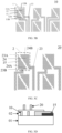
- the touch structure includes one or more first touch units 1 (e.g., the plurality of first touch units 1 are arranged in a plurality of rows and columns).
- the first touch unit 1 includes a first touch electrode 11 and a second touch electrode 12 that are adjacent to each other and insulated from each other.
- Each of the first touch electrode 11 and the second touch electrode 12 is self-capacitance electrode and includes a thin end (see 11A and 12A) and a thick end (see 11B and 12B) that are arranged opposite to each other.
- the touch structure further includes a first trace 13.
- the first trace 13 includes a first sub-trace 131 and a second sub-trace 132.
- the first touch electrode 11 is coupled with the first sub-trace 131
- the second touch electrode 12 is coupled with the second sub-trace 132, thus, the first touch electrode 11 and the second touch electrode 12 are coupled to a touch detection circuit (not illustrated) through the first sub-trace 131 and the second sub-trace 132, respectively.
- the touch structure further includes a plurality of electrode pins 16 coupled to the plurality of first traces 13 for connecting the respective first traces to the touch detection circuit.
- FIG. 1D is a schematic cross-sectional view of the touch structure illustrated in FIG. 1A .
- the cut line is the a-a' line illustrated in FIG. 1A .
- the touch structure further includes a black frame.
- the electrode lead 16 is located in an area where the black frame 15 is located to avoid being viewed by a user, which affects the appearance.
- first touch electrode layers 10 are a grid-like structure formed of metal.
- the first touch electrode 11 and the second touch electrode 12 are located in the same layer (see the first touch electrode layer 10) (the first touch electrode 11 and the second touch electrode 12 are located side by side on the carrier substrate 01 (see FIG. 1D )).
- the materials of the first touch electrode 11 and the second touch electrode 12 are the same.
- the first touch electrode 11 and the second touch electrode 12 may be formed by patterning a same film, which simplifies the manufacturing process of the touch structure.
- the patterning process is a photolithography process including exposure, development, and etching steps.
- the planar shapes of the first touch electrode 11 and the second touch electrode 12 are substantially the same and an edge of the first touch electrode and an edge of the second touch electrode that are closed to each other are substantially parallel to each other.
- the planar shape of the first touch electrode 11 and the second touch electrode 12 substantially have the same size and the same profiles, and each is substantially a right-angled triangle, so the areas of the first touch electrode 11 and the second touch electrodes 12 are substantially equal to each other. Because the edge of the first touch electrode 11 and the edge of the second touch electrode 12 that are closed to each other (i.e., the adjacent edges of the two) are substantially parallel, the planar shapes of the first touch electrode 11 and the second touch electrode 12 are complementary. This facilitates the determination of a touch position by using the first touch electrodes 11 and second touch electrode 12 and helps to increase the touch sensitivity and avoid erroneous determination.
- the touch structure includes a plurality of the first touch units 1 arranged in a plurality of rows and columns
- the thin ends 11A of a plurality of the first touch electrodes 11 located in the same row have the same orientation and are oriented toward the side facing away from the black frame 15
- the thin ends 12A of a plurality of the second touch electrodes 12 located in the same row have the same orientation and are oriented toward a side facing the black frame 15
- the second touch electrode 12 in the left first touch unit 1 has an edge adjacent to an edge of the first touch electrode 11 in the right first touch unit 1, and the two adjacent edges are substantially parallel to each other.
- the thin end of the first touch electrode 11 is close to the thick end of the second touch electrode 12, and the thick end of the first touch electrode 11 is close to the thin end of the second touch electrode 12.
- Such an arrangement helps to achieve a complementation between the planar shapes of the first touch electrode 11 and the second touch electrode 12.
- the planar shape of the first touch unit formed by complementing the first touch electrode 11 and the second touch unit 12 are substantially rectangle.
- the two right-angled sides of the touch electrode 11 and the second touch electrode 12 are both oriented outwardly and the oblique sides of the first touch electrode 11 and the second touch electrode 12 are parallel to each other.
- first touch electrodes 11 and the second touch electrodes 12 are complementary to each other and the arrangement of the plurality of first touch units 1 as illustrated in Fig. 1A are described for illustrative purposes only.
- the touch structure illustrated in FIG. 1A includes two rows and three columns of the first touch units 1. In the row direction, a gap is between every two adjacent first touch units 1, and the widths of the gaps are the same or not.
- the first sub-trace 131 and the second sub-trace 132 respectively coupled to the first touch electrode 11 and the second touch electrode 12 of the leftmost first touch unit 1 in the first row are located in a first gap, and the first sub-trace 131 coupled to the first touch electrode 11 of the middle first touch unit 1 in first row is also located in the first gap.
- the first gap is a gap between the leftmost first touch unit and the middle first touch unit in the second row.
- the first sub-trace 131 and the second sub-trace 132 respectively coupled to the first touch electrode 11 and the second touch electrode 12 of the rightmost first touch unit 1 in the first row, and the second sub-trace 132 coupled to the second touch electrode 12 of the middle first touch unit 1 in first row are located in a second gap.
- the second gap is a gap between the rightmost first touch unit and the middle first touch unit in the second row.
- the other three sides does not have a frame.
- the three-side frameless multi-point touch can be realized.
- Fig. 1B is a schematic top view of another touch structure according to the present disclosure.
- the planar shapes of the first touch electrode 11 and the second touch electrode 12 are substantially the same in shape and are both substantially right-angled triangles, and the longer right-angled sides of the first touch electrode 11 and the second touch electrode 12 are close to each other and substantially parallel to each other.
- the planar shapes of the first touch electrode 11 and the second touch electrode 12 have the substantially same profile and the substantially same size, so the areas of the first touch electrode 11 and the second touch electrode 12 are substantially equal to each other.
- the planar shapes of the first touch electrode 11 and the second touch electrode 12 are complementary. This facilitates the determination of a touch position by using the first touch electrodes 11 and second touch electrode 12 and helps to increase the touch sensitivity and avoid erroneous determination.
- the touch structure includes the plurality of the first touch units 1 arranged in a plurality of rows and columns
- the thin ends 11A of the plurality of the first touch electrodes 11 located in the same row have the same orientation and are oriented toward the side facing away from the black frame 15
- the thin ends 12A of the plurality of the second touch electrodes 12 located in the same row have the same orientation and are oriented toward a side facing the black frame 15
- the second touch electrode 12 in the left first touch unit 1 has an edge adjacent to an edge of the first touch electrode 11 in the right first touch unit 1, and the two adjacent edges are substantially parallel to each other.
- the thin end of the first touch electrode 11 is close to the thick end of the second touch electrode 12, and the thick end of the first touch electrode 11 is close to the thin end of the second touch electrode 12.
- Such an arrangement helps to achieve a mutual matching between the planar shapes of the first touch electrode 11 and the second touch electrode 12.
- the planar shape of the first touch unit formed by complementing the first touch electrode 11 and the second touch unit 12 is parallelogram.
- the right-angled sides of the touch electrode 11 and the second touch electrode 12 in the same first touch unit 1 are both oriented inwardly, the longer right-angled sides of the touch electrode 11 and the second touch electrode 12 are parallel to each other, and the oblique sides of the first touch electrode 11 and the second touch electrode 12 are oriented outwardly.
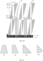
- Fig. 1C is a schematic top view of a first touch electrode or a second touch electrode according to the present disclosure.
- the profile of the shape of the first touch electrode or the second touch electrode seen from the top may be trapezoid (including an isosceles trapezoid (1) and a right-angled trapezoid (2)), a triangle (3), or a sector (4). It can be understood that the sides of each shape may include a concave-convex structure.
- the oblique side of the triangle (3) in FIG. 1C is serrated.
- the radius angle of the sector is 60 degrees or less.
- the principle of determining a touch position by using the touch structure will be described below with reference to Fig. 2A and Fig. 2B .
- the direction in which the shortest distance from the thin end to the thick end of each touch electrode is referred to as an extended length direction of the touch electrode, and the direction perpendicular to the extended length direction is referred to as a width direction of the touch electrode.
- the profiles of the shapes of the first touch electrode and the second touch electrode seen from the top are triangle.
- the touch electrode is divided into n regions (region 1, region 2 ..., region n) whose areas changes sequentially, and the n regions are substantially equal in size in the extended length direction.
- the extended length of the touch electrode can be divided according to the width of the thick end of the touch electrode (see W0 in Fig. 2A ).
- the size of the divided n regions along the extended length direction is substantially equal to W0, and for both the first touch electrode 11 and the second touch electrode 12, the ratio of the extended length L to the width W0 of the thick end is greater than or equal to n and less than n+1. That is, the ratio is in a range of [n, n+1), where n is a positive integer. For example, n is greater than or equal to 2. It can be understood that when the first touch electrode and the second touch electrode each seen from the top is in shape of a triangle, the width W0 of the thick end is the length of the shortest side of the triangle, and the extended length is the height corresponding to the shortest side of the triangle.
- the width W0 of the thick end is the length of the lower bottom side of the trapezoid
- the extended length is the height of the trapezoid.
- the width W0 of the thick end is the length of an arc corresponding to the sector
- the extended length is the radius of the circle where the sector is located.
- the areas of the region 1 to the region n is successively increased. Because the areas of the region 1 to the region n are different from one another, the amount of change in signals (i.e., the amount of change in self-capacitance) in the different regions due to the touch are different from one another. Therefore, the regions 1 to n correspond to n ranges in which the amount of change in signal is successively increased.
- a touch object for example, a user's finger
- the signals of the first touch electrode 11 and the second touch electrode 12 that are closest to the touch object are changed, and the touched position can be calculated according to the range where the amount of change in signals of the first touch electrode 11 and the second touch electrode 12 is located.
- the single touch can simultaneously cause three or more signals on the first touch electrodes 11 and the second touch electrodes 12 to change.
- the first touch electrode 11 and the second touch electrode 12 that are touched have thick ends and thin ends (for example, the first touch electrode 11 and the second touch electrode 12 are in shape of a wedge shape)
- the first touch electrode 11 and/or the second touch electrode 12 that is touched can be determined according to the amount of change in self-capacitance. An accurate detection of the touch position can be achieved according to which region of the touched first touch electrode 11 and/or the touched second electrode 12 is touched.
- a single touch simultaneously causes the signals of an electrode 1, an electrode 2 and an electrode 3 to change.
- the electrode 2 and the electrode 3 we know that a region 1 of the electrode 1 is touched, a region n of the electrode 2 is touched, and a region n of the electrode 3 is touched, and the touch position can be determined.
- it may be any one or two of the electrode 1, the electrode 2, and the electrode 3 that are touched.
- the principle of determining the touch position includes: in the case where no touch occurs, inputting a driving signal to the first touch electrodes and the second touch electrodes in each of the first touch units in the touch structure first, and then scanning the sensing signals of each of the first touch electrodes and each of the second touch electrodes to obtain basic signals; dividing each of the first touch electrodes and each of the second touch electrodes into n regions along the extended length direction thereof (as illustrated in FIG.
- the signal variation ranges corresponding to the amount of change in signals of the n regions that is, obtaining n ranges; after that, detecting all the first touch electrodes and the second touch electrodes whose signals are changed to obtain the touched electrodes, (for example, the signals of the electrode 1, the electrode 2 and the electrode 3 in FIG. 2B are changed while the signals of the other electrodes are not changed, and thus the electrode 1, the electrode 2 and the electrode 3 are touched electrodes); finally, determining the touch position according to the positional relationship among the plurality of touched electrodes and the amount of change in signal of each touched electrode (for example, it can be determined that the region 1 of the electrode 1, the region n of the electrode 2, and the region n of the electrode 3 in FIG. 2B are touched and thus the touch position can be determined (see position of the solid circle in Fig. 2B ).
- a single touch causes changes in signals of the plurality of the first touch electrodes and/or changes in signals of the second touch electrodes.
- the touch position can be determined by analyzing the change in signals of the plurality of first touch electrodes and/or the changes in signals of second touch electrodes.
- the first touch electrodes and/or the second touch electrodes with changed signals and corresponding to the different positions are different, and therefore these positions can be accurately determined. That is, multi-touch can be realized.
- the touch position can still be determined by analyzing the signal variation range in which the amount of change in signal of the touch electrode is located.
- the touch position can be determined by performing a single touch to cause changes in signals of the plurality of first touch electrodes and/or changes in signals of second touch electrodes.
- the contact area between the finger and the touch structure is about 5 mm*5 mm (millimeter).
- the width W0 of the thick end of the touch electrode may be set to be greater than or equal to 4 mm and less than or equal to 8 mm.
- the size of each of the first touch units 1 in the row direction is approximately from 4 mm to 8 mm.
- the distance between the first touch electrode and the second touch electrode that are adjacent is not too long.
- a gap 14 is provided between the first touch electrode 11 and the second touch electrode 12 (for example, the gap is filled with an insulating material), and the width of the gap 14 (see w in FIG. 1A ) is less than or equal to 30 ⁇ m (micrometers).
- the width of the gap 14 is, for example, greater than or equal to 5 ⁇ m, which is limited by the precision of the photolithography process itself.
- the interior of the profiles of the planar shapes of the first touch electrode 11 and the second touch electrode 12 are in a grid shape.
- Using a wedge-shaped touch electrode that is in a grid shape as a whole helps to increase the transmittance of the touch structure.
- the materials of the first touch electrode 11 and the second touch electrode 12 are both metal. Due to the good ductility of the metal, the use of the first touch electrode 11 and the second touch electrode 12 that are in a grid shape and made of a metal makes the touch structure suitable for use in a flexible touch device (for example, a flexible touch display device).
- the carrier substrate 01 is a transparent flexible substrate for use in a flexible touch device.
- the first touch electrode 11 and the second touch electrode 12 may be made of material comprising at least one of aluminum, aluminum alloy, copper, copper alloy, ferrum, zirconium, or titanium.
- the first touch electrode 11 and the second touch electrode 12 each include a plurality of wires intersecting one another to form a grid shape, the grid shape has a plurality of closed hollow portions.
- the wires constituting the grid pattern are inclined with respect to the row direction and the column direction.
- each of the first traces 13 is a grid shape, and the hollow portion in the grid shape allow the first traces 13 to be less visible to the user.
- the first trace 13 is made of a metal material.
- the first trace 13 may be made of material comprising aluminum, aluminum alloy, copper, copper alloy, ferrum, zirconium, or titanium.
- the first trace 13, the first touch electrode 11 and the second touch electrode 12 are located in the same layer 10 and are made of the same material, and thus the first trace 13, the first touch electrode 11 and the second touch electrode 12 may be formed by the same patterning process using the same film, which simplifies the manufacturing process and reduces the production cost.
- a plurality of electrode pins 16 are located on the same side of the touch area surrounded by the plurality of first touch units 1 (see the side on which the black frame 15 is disposed in FIG. 1A ).
- the plurality of first traces 13 are extended in the touch area and leaves the touch area from the side of the touch area same as the electrode pins 16 so as to electrically connect to the electrode pins 16. That is, each of the first traces 13 includes a first end coupled to the corresponding first touch electrode or the second touch electrode, a second end coupled to the electrode pin 16, and an extending portion between the first end and the second end.
- the extending portion is extended within the touch areas and is coupled to the electrode pin 16 after leaving from the side of the touch area same as the black frame 15 (the side is the length direction side of the black frame 15) .
- a three-sided frameless structure for example, a flexible three-sided frameless multi-touch screen
- the electrode pins 16 are made of a metal material.
- the electrode pins 16, the first traces 13, the first touch electrodes 11, and the second touch electrodes 12 are all formed from the same metal layer by using the same patterning process so as to simplify the fabrication process and reduce the production cost.
- the inventor of the present application noticed that if the touch structure is used to recognize the touch of the active pen, the size of the touch unit needs to be reduced to about 4 mm to obtain higher touch sensitivity. However, this may result in a wider frame.
- At least one embodiment of the present disclosure further provides another touch structure including two touch electrode layers to achieve higher sensitivity.
- the touch structure can recognize the touch of the active pen.
- the traces in the two touch electrode layers it is possible to achieve a narrow frame or a three-sided borderless structure while achieving higher sensitivity. Description will be made below with reference to Figs. 3A to 3D .
- the touch structure includes the first touch unit 1, and further includes a second touch unit 2.
- the second touch unit 2 includes a third touch electrode 27 and a fourth touch electrode 24 that are adjacent to each other and insulated from each other.
- Both the third touch electrode 27 and the fourth touch electrode 24 are self-capacitance electrodes and include a thin end and a thick end that are arranged opposite to each other.
- the touch structure further includes a plurality of second traces 23 and a plurality of electrode pins 26 respectively coupled to the second traces 23.
- the plurality of second traces 23 include a third sub-trace 231 and a fourth sub-trace 232.
- the third touch electrode 27 is coupled to the third sub-trace 231
- the fourth touch electrode 24 is coupled to the fourth sub-trace 232, thus, the third touch electrode 27 and the fourth touch electrode 24 are coupled to the touch detection circuit through the respective second trace and the respective electrode pin 26.
- the second touch unit 2 and the first touch unit 1 are located in different layers, that is, the second touch unit 2 and the first touch unit 1 are formed of films on different layers.
- the first touch electrode 11 and the second touch electrode 12 in the first touch unit 1 are located in the first touch electrode layer 10
- the third touch electrode 27 and the fourth touch electrode 24 in the second touch unit 2 are located in the second touch electrode layer 20.
- the first touch electrode layer 10 is covered by an insulating layer (e.g., a transparent insulating layer) 02
- the second touch electrode layer 20 is located on a side of the insulating layer 02 away from the first touch electrode layer 10.
- the second touch unit 2 is located at a position corresponding to the gap between the two adj acent first touch units 1 in the row direction. That is, the orthographic projection of the second touch unit 2 on the carrier substrate 01 is located between the orthographic projections, on the carrier substrate 01, of the two first touch units 1 adjacent to each other in the row direction.
- the sizes of the first touch unit 1 and of the second touch unit 2 both in the row direction and in the column direction are in a range from 4 mm to 5 mm, for example, in a range from 4 mm to 4.5 mm.
- the distance between the two first touch units 1 adjacent to each other is also in a range from 4 mm to 5 mm.
- the design illustrated in FIG. 3A to FIG. 3D is adopted.
- the touch position can be determined by the second touch unit 2 located between the two adjacent first touch units 1, because the first touch unit 1 and the second touch unit 2 are complementary with each other. Therefore, the design can effectively increase the touch sensitivity, and thus the touch object can be recognized by the touch units when the touch object touches any point in the touch area. Due to the complementation between the electrode layer 10 and the electrode layer 20, the signal change in any function area of the display screen can be effectively recognized at the time of touch.
- the manner in which the first touch unit 1 and the second touch unit 2 are located in different touch electrode layers allows the size of each of the first touch unit 1 and each of the second touch units 2 to be designed to be smaller, so that the touch of the active pen can be recognized.
- the manner in which the first touch unit 1 and the second touch unit 2 are located in different touch electrode layers allows the distance between the two first touch units adjacent to each other to be relatively large (for example, from 4 mm to 5 mm), and allows the distance between the two second touch units adjacent to each other to be relatively large (for example, from 4 mm to 5 mm).
- the first trace 13 and the second traces 23 can be arranged in different layers rather than being sequentially arranged on the same layer.
- the width of the first traces 13 and the width of the second traces 23 can be larger, which effectively reduces the impedance.
- the planar shape, the material, and the size of the third touch electrode 27 and the fourth touch electrode 24 may be configured by referring to those of the first touch electrode 11 and the second touch electrode 12, and the repeated description is omitted.
- the planar shape for example, the second trace 23 is a grid shape
- the position for example, the second trace is extended within the touch area and leaves the touch area from the side of the touch area same as the black frame 15
- other parameters of the second trace 23 may be configured by referring to those of the first trace 13, and the repeated description is omitted.
- the first touch electrode 11, the second touch electrode 12, the third touch electrode 27, and the fourth touch electrodes 24 are all made of metal, and both the first traces 13 and the second traces 23 are extended within the touch area and leave the touch area from the side of the touch area close to the electrode pin 16, 26, so as to electrically connect the touch detection circuit.
- a flexible three-sided frameless multi-touch screen for determining the touch of the active pen can be realized.
- the present disclosure further provides a touch device including the touch structure provided by any of the above embodiments.
- the touch device can be an add-on touch display device, an on-cell touch display device, or an in-cell touch display device.
- the touch device may be a liquid crystal touch panel, an electronic paper, an OLED (Organic Light-Emitting Diode) touch panel, a mobile phone, a tablet computer, a television, a display, a notebook computer, a digital photo frame, a navigator and any product or component with touch function.
- OLED Organic Light-Emitting Diode
- the present disclosure further provides a method for manufacturing a touch structure.
- the touch structures illustrated in FIGS 3A to 3D are taken as an example.
- the manufacturing method includes: forming the first touch electrode layer 10.
- the first touch electrode layer 10 includes the first touch unit 1 and the plurality of first traces 13.
- the first touch unit 1 includes the first touch electrode 11 and the second touch electrode that are adjacent to each other and insulated from each other.
- Both the first touch electrode 11 and the second touch electrode 12 are self-capacitance electrodes and include the thin end (see 11A and 12A) and the thick end (see 11B and 12B) that are arranged opposite to each other. Additionally, the first touch electrode 11 and the second touch electrode 12 are coupled to the first sub-trace 131 and the second sub-trace 132, respectively.
- the manufacturing method provided by at least one embodiment of the present disclosure includes the following steps S11 to S12.
- Step S11 forming the black frame 15 on the carrier substrate 01, as illustrated in FIG. 1D .
- the carrier substrate 01 is a transparent flexible substrate.
- Step S12 forming a metal layer on the carrier substrate 01, and performing a patterning process (for example, a photolithography process) on the metal layer by using a photomask to form the first touch electrode layer 10, as illustrated in FIGS. 1A and 1D .
- a patterning process for example, a photolithography process
- the first touch electrode layer 10 includes the first touch electrode 11, the second touch electrode 12, the first trace 13, and the electrode pin 16.
- the main bodies of the first touch electrode 11 and of the second touch electrode 12 are in a grid shape.
- the manufacturing method provided by the present disclosure may be used to simultaneously fabricate a plurality of touch structures at a time.
- the manufacturing method further includes the step S13: cutting a mother board obtained after completing the step S12 into a plurality of sub-boards, each of the sub-boards includes the touch structure.
- Tthe manufacturing method provided by the present disclosure further includes, after completing the above step S13, electrically connecting a flexible printed circuit board (FPC) which is coupled to the touch detection circuit (e.g., an integrated circuit) to the electrode pins 16 on the carrier substrate 01.
- FPC flexible printed circuit board
- a single-layer (i.e., only one layer of touch electrode layer) multi-touch screen with a narrow frame, or a three-sided frameless single-layer multi-touch screen can be obtained.
- the manufacturing method further includes: forming the second touch electrode layer 20.
- the second touch electrode layer 20 includes the second touch unit 2 and the plurality of the second traces 23.
- the second touch unit includes the third touch electrode 27 and the fourth touch electrode 24 that are adjacent to each other and insulated from each other.
- the third touch electrode 27 and the fourth touch electrode 24 are both self-capacitance electrodes and both include the thin end and the thick end that are arranged opposite to each other.
- the third touch electrode 27 and the fourth touch electrode 24 are respectively coupled with the third sub-trace 231 and the fourth sub-trace 232.
- the second touch unit 2 is located at a position corresponding to the gap between two adjacent first touch units 1.
- the manufacturing method provided by at least one embodiment of the present disclosure includes the following steps S21 to S24.
- Step S11 forming the black frame 15 on the carrier substrate 01, as illustrated in FIG. 3D .
- the carrier substrate 01 is a transparent flexible substrate.
- Step S22 forming a first metal layer on the carrier substrate 01, and performing a patterning process (for example, a photolithography process) on the first metal layer by using a first photomask to form the first touch electrode layer 10, as illustrated in FIGS. 3A and 3B .
- a patterning process for example, a photolithography process
- the first touch electrode layer 10 includes the first touch electrode 11, the second touch electrode 12, the first trace 13, and the electrode pin 16.
- the main bodies of the first touch electrode 11 and of the second touch electrode 12 are in a grid shape.
- Step S23 forming the insulating layer 02 covering the first touch electrode layer 10 by using a second photomask, and the insulating layer 02 does not cover the area where the black frame 15 is located (i.e., the bonding area).
- the insulating layer 02 is a transparent insulating layer.
- the insulating layer 02 covers the entire touch area.
- Step S24 forming a second metal layer on the insulating layer 02, and performing a patterning process (for example, a photolithography process) on the second metal layer by using a third photomask to form the second touch electrode as illustrated in FIG. 3A and FIG. 3C .
- a patterning process for example, a photolithography process
- the second touch electrode layer 20 includes the third touch electrode 27, the fourth touch electrode 24, the second trace 23, and the electrode pin 26, and the third touch electrode 27 and the fourth touch electrode 24 are in a grid shape as a whole.
- the manufacturing method provided by at least one embodiment of the present disclosure may be used to simultaneously fabricate a plurality of touch structures at a time.
- the manufacturing method further includes the step S25: cutting a mother board obtained after completing the step S24 into a plurality of sub-boards, each of the sub-boards includes the touch structure.
- the manufacturing method provided by at least one embodiment of the present disclosure further includes, after completing the above step S25, electrically connecting a flexible printed circuit board (FPC) which is coupled to the touch detection circuit (e.g., an integrated circuit) to the electrode pins 16 and 26 on the carrier substrate 01.
- FPC flexible printed circuit board
- a double-layer multi-point touch screen with narrow frame, or a three-sided frameless double-layer multi-point touch screen can be realized.
- FIG. 4 is flowchart of a method for determining a touch position. As illustrated in FIG. 4 , the method for determining a touch position includes step S41 and step S42.
- Step S41 determining the touched electrode, according to the amount of change in self-capacitances of the first touch electrode and of the second touch electrode included in the first touch unit.
- the basic signal is detected through the first trace.
- the change in the self-capacitance of the first touch electrode and the change in the self-capacitance of the second touch electrode can be determined by comparing the detection signals of the first touch electrode and/or the second touch electrode with the basic signal respectively, and thus the touched electrode is determined.
- the driving signal is input to all the first touch electrodes and all the second touch electrodes in the touch structure first, and then the sensing signal of each of the first touch electrodes and each of the second touch is scanned to obtain the basic signal.
- Step S42 determining the touch position, according to the amount of change in self-capacitance of each region of the touched electrode.
- the touched electrode has the thick end and the thin end the touched electrode is in shape of a wedge shape
- the amount of change in self-capacitance of the different regions of the touched electrode are different when the different regions are touched.
- FIG. 5 is a flowchart of a method for determining a touch position according to at least one embodiment of the present disclosure. As illustrated in FIG. 5 , the touch positioning method includes step S51 and step S52.
- Step S51 determining the touched electrode, according to the amount of change in self-capacitances of the first touch electrode and of the second touch electrode included in the first touch unit and the amount of change in self-capacitances of the third touch electrode and of the fourth touch electrode included in the second touch unit.
- the basic signal is detected through the first trace and the second trace; in the case that at least one of the first touch electrode, the second touch electrode, the third touch electrode, and the fourth touch electrode is touched, the change in the self-capacitance of the first touch electrode, the change in the self-capacitance of the second touch electrode, the change in the self-capacitance of the third touch electrode, and the change in the self-capacitance of the fourth touch electrode can be determined by comparing the detection signals of the first touch electrode, the second touch electrode, the third touch electrode, and the fourth touch electrode with the basic signal respectively, and thus the touched electrode is determined.
- the driving signal is input to all the first touch electrodes, all the second touch electrodes, all the third touch electrodes, and all the fourth touch electrodes in the touch structure first, and then the sensing signals of each of the first touch electrodes, each of the second touch electrodes, each of the third touch electrodes, and each of the fourth touch electrodes are scanned to obtain a basic signal.
- Step S52 determining the touch position according to the amount of change in self-capacitance of each region of the touched electrode.
- the touched electrode has the thick end and the thin end (the touched electrode is in shape of a wedge shape), the amount of change in self-capacitance of the different regions of the touched electrode are different when the different regions are touched.
- the amount of change in self-capacitance of each region of the touched electrode it is possible to determine which region of the touched electrode is touched so as to determine the touched position.
- the method for determining a touch position includes: in the case that no touch occurs, inputting a driving signal to all the touch electrodes in the touch structure and then scanning the sensing signals of each of the touch electrodes to obtain the basic signals; dividing each of the touch electrodes into n regions along the extended length direction thereof (as illustrated in FIG. 2A ) and determining the signal variation ranges respectively corresponding to the n regions, that is, obtaining n ranges; after that, detecting all the touch electrodes whose signals are changed to obtain the touched electrodes (the signals of the electrode 1, the electrode 2 and the electrode 3 in FIG.
- the embodiment of the present disclosure provides a touch structure and a method for manufacturing the touch structure, a touch device, a method for determining a touch position.
- the touch structure includes a first touch unit and a first trace.
- the first touch unit includes a first touch electrode and a second touch electrode that are both self-capacitance electrodes and both have a thin end and a thick end that are arranged opposite to each other.
- the first touch electrode and the second touch electrode are coupled to different first traces.
- the touch structure can realize multi-touch, for example, realizing a flexible three-sided frameless multi-point touch screen.
- a touch structure with a higher sensitivity can be realized, for example, a flexible three-sided frameless multi-touch screen that can recognize a touch position of an active pen is realized.
- the touch structure and the method for manufacturing the touch structure, the touch device and the method for determining a touch position provided by the embodiment of the present disclosure may be mutually referenced.
Landscapes
- Engineering & Computer Science (AREA)
- General Engineering & Computer Science (AREA)
- Theoretical Computer Science (AREA)
- Human Computer Interaction (AREA)
- Physics & Mathematics (AREA)
- General Physics & Mathematics (AREA)
- Computer Networks & Wireless Communication (AREA)
- Position Input By Displaying (AREA)
- Switches That Are Operated By Magnetic Or Electric Fields (AREA)
Claims (10)
- Berührungsstruktur zur Bestimmung einer Berührungsposition, umfassend:eine Vielzahl von ersten Berührungseinheiten (1), die in einer Reihe angeordnet sind, wobei jede der ersten Berührungseinheiten (1) eine erste Berührungselektrode (11) und eine zweite Berührungselektrode (12) umfasst, wobei die erste Berührungselektrode (11) und die zweite Berührungselektrode (12) einander benachbart und voneinander isoliert sind, und die erste Berührungselektrode (11) und die zweite Berührungselektrode (12) beide Eigenkapazitätselektroden sind und beide ein schmales Ende (11A, 11B) und ein breites Ende (12A, 12B) umfassen, die einander gegenüber angeordnet sind;einen ersten Leiterbahnsatz (13), der eine Vielzahl von ersten Leiterbahnen (131) und eine Vielzahl von zweiten Leiterbahnen (132) umfasst,wobei eine erste Leiterbahn (131) mit einer ersten Berührungselektrode (11) gekoppelt ist und eine zweite Leiterbahn (132) mit einer zweiten Berührungselektrode (12) gekoppelt ist, wobei die erste Berührungselektrode und die zweite Berührungselektrode die Form eines Keils aufweisen, dadurch gekennzeichnet, dass die Berührungsstruktur weiterhin umfasst:eine Vielzahl von zweiten Berührungseinheiten (2), die in einer Reihe angeordnet sind, wobei jede der zweiten Berührungseinheiten (2) eine dritte Berührungselektrode (27) und eine vierte Berührungselektrode (24) umfasst, wobei die dritte Berührungselektrode (27) und die vierte Berührungselektrode (24) einander benachbart und voneinander isoliert sind, und die dritte Berührungselektrode (27) und die vierte Berührungselektrode (24) beide Eigenkapazitätselektroden sind und beide ein schmales Ende (23A, 24A) und ein breites Ende (23B, 24B) umfassen, die einander gegenüber angeordnet sind; undeinen zweiten Leiterbahnsatz (23), der eine Vielzahl von dritten Leiterbahnen (231) und eine Vielzahl von vierten Leiterbahnen (232) umfasst,wobei eine dritte Leiterbahn (231) mit einer dritten Berührungselektrode (27) gekoppelt ist und eine vierte Leiterbahn (232) mit einer vierten Berührungselektrode (24) gekoppelt ist,wobei die zweiten Berührungseinheiten (2) in einer Schicht angeordnet sind, die sich von den ersten Berührungseinheiten (1) unterscheidet, und die zweiten Berührungseinheiten (2) an einer Position angeordnet sind, die einer Lücke zwischen den ersten Berührungseinheiten (1) entspricht, die in einer Reihenrichtung benachbart sind.
- Berührungsstruktur nach Anspruch 1, wobei das Verhältnis einer ausgedehnten Länge (L) der ersten Berührungselektrode (11) von dem schmalen Ende (11A) zu dem breiten Ende (11B) zu einer Breite (W0) des breiten Endes (11B) in einem Bereich von n bis n+1 liegt, und ein Verhältnis einer ausgedehnten Länge der zweiten Berührungselektrode (12) von dem schmalen Ende (12A) zu dem breiten Ende (12B) zu einer Breite des breiten Endes (12B) in einem Bereich von n bis n+1 liegt, wobei n eine positive ganze Zahl ist, wobei die Richtung, in der der kürzeste Abstand von dem schmalen Ende (11A) zu dem breiten Ende (11B) jeder Berührungselektrode (11) eine ausgedehnte Längenrichtung der Berührungselektrode (11) ist.
- Berührungsstruktur nach Anspruch 1 oder 2, wobei die Berührungsstruktur eine Vielzahl von ersten Berührungseinheiten (1) umfasst und die Vielzahl von ersten Berührungseinheiten (1) in einem Array angeordnet sind.
- Berührungsstruktur nach Anspruch 3, wobei die schmalen Enden (11A) einer Vielzahl der ersten Berührungselektroden (11), angeordnet in einer gleichen Reihe, eine gleiche Ausrichtung aufweisen, und die schmalen Enden (12A) einer Vielzahl der zweiten Berührungselektroden (12), angeordnet in einer gleichen Reihe, eine gleiche Ausrichtung aufweisen.
- Berührungssteuerungsstruktur nach Anspruch 4, wobei bei zwei ersten Berührungseinheiten (1), die einander benachbart und in derselben Reihe angeordnet sind, eine Kante der zweiten Berührungselektrode (12) in einer der zwei ersten Berührungseinheiten (1) an eine Kante der ersten Berührungselektrode (11) in der anderen der zwei ersten Berührungseinheiten (1) angrenzt und zwei benachbarte Kanten parallel zueinander sind.
- Berührungsstruktur nach einem der Ansprüche 3 bis 5, weiterhin umfassend: eine Vielzahl von Elektrodenstiften (16), die so konfiguriert sind, dass sie mit einer Vielzahl der ersten Verdrahtungen (13) gekoppelt sind, wobei die Vielzahl von Elektrodenstiften (16) sich auf einer Seite einer Berührungsfläche befinden, die der Vielzahl erster Berührungseinheiten (1) entspricht, und die Vielzahl der ersten Verdrahtungen (13) so konfiguriert sind, dass sie sich innerhalb der Berührungsfläche erstrecken und die Berührungsfläche von der Seite der Berührungsfläche verlassen, die der Vielzahl von Elektrodenstiften (16) entspricht.
- Berührungsvorrichtung, die die Berührungsstruktur nach einem der Ansprüche 1 bis 6 umfasst.
- Verfahren zur Herstellung einer Berührungsstruktur zur Bestimmung einer Berührungsposition, umfassend:Bilden einer ersten Berührungselektrodenschicht (10), wobei die erste Berührungselektrodenschicht (10) eine Vielzahl von ersten Berührungseinheiten (1) und einen ersten Leiterbahnsatz (13) umfasst, jede der ersten Berührungseinheiten (1) eine erste Berührungselektrode (11) und eine zweite Berührungselektrode (12) umfasst, die aneinander angrenzen und voneinander isoliert sind, die erste Berührungselektrode (11) und die zweite Berührungselektrode (12) beide Eigenkapazitätselektroden sind und beide ein schmales Ende (11A, 11B) und ein breites Ende (12A, 12B) umfassen, die einander gegenüberliegend angeordnet sind, der erste Leiterbahnsatz (13) eine Vielzahl von ersten Leiterbahnen (131) und eine Vielzahl von zweiten Leiterbahnen (132) umfasst, eine erste Leiterbahn (131) mit einer ersten Berührungselektrode (11) gekoppelt ist, und eine zweite Leiterbahn (132) mit einer zweiten Berührungselektrode (12) gekoppelt ist, wobei die erste Berührungselektrode und die zweite Berührungselektrode die Form eines Keils aufweisen,dadurch gekennzeichnet, dass das Verfahren weiterhin umfasst:Bilden einer zweiten Berührungselektrodenschicht (20), wobei die zweite Berührungselektrodenschicht (20) eine Vielzahl von zweiten Berührungseinheiten (2) und einen zweiten Leiterbahnsatz (23) umfasst,jede der zweiten Berührungseinheiten (2) eine dritte Berührungselektrode (27) und eine vierte Berührungselektrode (24) umfasst, die aneinander angrenzen und voneinander isoliert sind, die dritte Berührungselektrode (27) und die vierte Berührungselektrode (24) beide Eigenkapazitätselektroden sind und beide ein schmales Ende (23A, 24A) und ein breites Ende (23B, 24B) umfassen, die einander gegenüberliegend angeordnet sind, der zweite Leiterbahnsatz (23) eine Vielzahl von dritten Leiterbahnen (231) und eine Vielzahl von vierten Leiterbahnen (232) umfasst, eine dritte Leiterbahn (231) mit einer dritten Berührungselektrode (27) gekoppelt ist, eine vierte Leiterbahn (232) mit einer vierten Berührungselektrode (24) gekoppelt ist; die zweiten Berührungseinheiten (2) in einer Schicht (20) angeordnet sind, die sich von den ersten Berührungseinheiten (1) unterscheidet, und die zweiten Berührungseinheiten (2) an einer Position angeordnet sind, die einer Lücke zwischen den ersten Berührungseinheiten (1) entspricht, die in einer Reihenrichtung benachbart sind.
- Verfahren zur Bestimmung einer Berührungsposition unter Verwendung der Berührungsstruktur nach einem der Ansprüche 1 bis 8, umfassend:Bestimmen (S41) einer Elektrode, die berührt wird, gemäß einem Änderungsbetrag einer Eigenkapazität von jeder der ersten Berührungselektrode (11) in der ersten Berührungseinheit (1) und einem Änderungsbetrag einer Eigenkapazität von jeder der zweiten Berührungselektrode (12) in der ersten Berührungseinheit (1);Bestimmen einer Berührungsposition gemäß dem Änderungsbetrag der Eigenkapazität von jeder Region (Region 1, 2, ..., n) der Elektrode, die berührt wird (S42).
- Verfahren zur Bestimmung einer Berührungsposition unter Verwendung der Berührungsstruktur nach Anspruch 1, umfassend:Bestimmen (S51) einer Elektrode, die berührt wird, gemäß einem Änderungsbetrag einer Eigenkapazität von jeder der ersten Berührungselektrode (11) in der ersten Berührungseinheit (1) und einem Änderungsbetrag einer Eigenkapazität von jeder der zweiten Berührungselektrode (12) in der ersten Berührungseinheit (1) und einem Änderungsbetrag einer Eigenkapazität von jeder der dritten Berührungselektrode (27) in der zweiten Berührungseinheit (2) und einem Änderungsbetrag der vierten Berührungselektrode (24) in der zweiten Berührungseinheit (2);Bestimmen (S52) einer Berührungsposition gemäß dem Änderungsbetrag der Eigenkapazität von jeder Region (Region 1, 2, ..., n) der Elektrode, die berührt wird.
Applications Claiming Priority (2)
| Application Number | Priority Date | Filing Date | Title |
|---|---|---|---|
| CN201810204720.8A CN110275647B (zh) | 2018-03-13 | 2018-03-13 | 触控结构及其制作方法、触控装置和触摸定位方法 |
| PCT/CN2018/116225 WO2019174295A1 (zh) | 2018-03-13 | 2018-11-19 | 触控结构及其制作方法、触控装置和触摸定位方法 |
Publications (3)
| Publication Number | Publication Date |
|---|---|
| EP3767446A1 EP3767446A1 (de) | 2021-01-20 |
| EP3767446A4 EP3767446A4 (de) | 2021-12-08 |
| EP3767446B1 true EP3767446B1 (de) | 2024-02-21 |
Family
ID=67907297
Family Applications (1)
| Application Number | Title | Priority Date | Filing Date |
|---|---|---|---|
| EP18897867.0A Active EP3767446B1 (de) | 2018-03-13 | 2018-11-19 | Berührungsstruktur und herstellungsverfahren dafür, berührungsvorrichtung und berührungspositionierungsverfahren |
Country Status (4)
| Country | Link |
|---|---|
| US (1) | US11543925B2 (de) |
| EP (1) | EP3767446B1 (de) |
| CN (1) | CN110275647B (de) |
| WO (1) | WO2019174295A1 (de) |
Families Citing this family (3)
| Publication number | Priority date | Publication date | Assignee | Title |
|---|---|---|---|---|
| CN111427475B (zh) * | 2020-03-26 | 2022-09-02 | 京东方科技集团股份有限公司 | 触控模组、触控显示屏及触控显示屏的制造方法 |
| US11449183B1 (en) * | 2021-06-17 | 2022-09-20 | Sharp Display Technology Corporation | Touch panel sensor with optimal electrode separation for improved performance |
| KR20240000683A (ko) * | 2022-06-23 | 2024-01-03 | 삼성디스플레이 주식회사 | 표시장치 |
Family Cites Families (15)
| Publication number | Priority date | Publication date | Assignee | Title |
|---|---|---|---|---|
| US6297811B1 (en) * | 1999-06-02 | 2001-10-02 | Elo Touchsystems, Inc. | Projective capacitive touchscreen |
| US20130154996A1 (en) * | 2011-12-16 | 2013-06-20 | Matthew Trend | Touch Sensor Including Mutual Capacitance Electrodes and Self-Capacitance Electrodes |
| US8829926B2 (en) * | 2012-11-19 | 2014-09-09 | Zrro Technologies (2009) Ltd. | Transparent proximity sensor |
| CN103268179B (zh) * | 2013-05-02 | 2016-05-25 | 京东方科技集团股份有限公司 | 触控电极及制作方法、电容式触控装置和触摸显示装置 |
| CN203224862U (zh) * | 2013-05-02 | 2013-10-02 | 京东方科技集团股份有限公司 | 触控电极结构、电容式触控装置和触摸显示装置 |
| CN203643988U (zh) * | 2013-09-13 | 2014-06-11 | 敦泰科技有限公司 | 电容式触摸显示装置 |
| JP2015106240A (ja) * | 2013-11-29 | 2015-06-08 | 富士フイルム株式会社 | 導電性フイルム及びタッチパネル |
| TWI507959B (zh) * | 2014-03-14 | 2015-11-11 | Mstar Semiconductor Inc | 配合自容式觸控面板之校正裝置及校正方法 |
| CN104503653B (zh) * | 2015-01-26 | 2017-04-19 | 京东方科技集团股份有限公司 | 一种自电容触摸屏和显示装置 |
| CN205353969U (zh) * | 2015-07-10 | 2016-06-29 | 宸鸿科技(厦门)有限公司 | 一种具有压力侦测的触控总成 |
| CN105278748A (zh) | 2015-10-19 | 2016-01-27 | 京东方科技集团股份有限公司 | 一种oled基板、显示装置、可穿戴设备、驱动方法以及补偿电路 |
| US10162994B2 (en) * | 2016-01-15 | 2018-12-25 | Raydium Semiconductor Corporation | Capacitive fingerprint sensing apparatus |
| CN106502466B (zh) * | 2016-10-28 | 2020-04-14 | 上海天马有机发光显示技术有限公司 | 一种触控装置、电子设备以及制作方法 |
| CN206312114U (zh) * | 2016-10-31 | 2017-07-07 | 南昌欧菲光科技有限公司 | 触摸屏及其悬浮触控组件 |
| CN206388155U (zh) * | 2016-11-28 | 2017-08-08 | 北京集创北方科技股份有限公司 | 触摸感应装置 |
-
2018
- 2018-03-13 CN CN201810204720.8A patent/CN110275647B/zh active Active
- 2018-11-19 EP EP18897867.0A patent/EP3767446B1/de active Active
- 2018-11-19 US US16/477,588 patent/US11543925B2/en active Active
- 2018-11-19 WO PCT/CN2018/116225 patent/WO2019174295A1/zh not_active Ceased
Also Published As
| Publication number | Publication date |
|---|---|
| WO2019174295A1 (zh) | 2019-09-19 |
| US11543925B2 (en) | 2023-01-03 |
| EP3767446A4 (de) | 2021-12-08 |
| CN110275647B (zh) | 2021-01-12 |
| CN110275647A (zh) | 2019-09-24 |
| US20210405812A1 (en) | 2021-12-30 |
| EP3767446A1 (de) | 2021-01-20 |
Similar Documents
| Publication | Publication Date | Title |
|---|---|---|
| EP2770409B1 (de) | Berührungsbildschirm und Herstellungsverfahren dafür | |
| US8557508B2 (en) | Method of fabricating capacitive touch panel | |
| KR102028157B1 (ko) | 플렉서블 터치 스크린 패널 이를 구비한 플렉서블 표시장치 | |
| KR101530794B1 (ko) | 3d 터치 제어 액정 렌즈 격자, 그 제조 방법, 및 3d 터치 제어 디스플레이 장치 | |
| KR101330779B1 (ko) | 터치 패널의 전극 구조, 그 방법 및 터치 패널 | |
| US20120299868A1 (en) | High Noise Immunity and High Spatial Resolution Mutual Capacitive Touch Panel | |
| US20160274703A1 (en) | Conductive sheet, capacitive touch panel, and display device | |
| US20140347319A1 (en) | Touch panel | |
| EP3686717A1 (de) | Berührungstafel und herstellungsverfahren dafür und berührungsanzeigetafel | |
| KR20160099791A (ko) | 터치 패널 및 이를 포함하는 표시 장치 | |
| EP3767446B1 (de) | Berührungsstruktur und herstellungsverfahren dafür, berührungsvorrichtung und berührungspositionierungsverfahren | |
| KR20120080390A (ko) | 터치 스크린 패널 | |
| US20150062449A1 (en) | Touch panel | |
| JP5472858B2 (ja) | タッチスイッチ | |
| US11775125B2 (en) | Touch electrode structure, touch screen and touch display device | |
| JP2015122046A (ja) | タッチパネル及びその製造方法、並びにタッチスクリーン装置 | |
| KR102245826B1 (ko) | 플렉서블 터치 스크린 패널 이를 구비한 플렉서블 표시장치 | |
| CN105912176A (zh) | 一种触控电极结构、触摸屏及显示装置 | |
| EP3640776A1 (de) | Berührungsbildschirm und verfahren zur herstellung davon, berührungsanzeigevorrichtung | |
| KR102281616B1 (ko) | 터치 스크린 패널 및 터치 스크린 패널 제조 방법 | |
| KR101293165B1 (ko) | 접촉 감지 패널 | |
| TWI554934B (zh) | 觸控面板 | |
| JP7394328B2 (ja) | タッチセンサ | |
| JP2012018516A (ja) | 入力装置 | |
| US10503333B2 (en) | Touch panel |
Legal Events
| Date | Code | Title | Description |
|---|---|---|---|
| STAA | Information on the status of an ep patent application or granted ep patent |
Free format text: STATUS: UNKNOWN |
|
| STAA | Information on the status of an ep patent application or granted ep patent |
Free format text: STATUS: THE INTERNATIONAL PUBLICATION HAS BEEN MADE |
|
| PUAI | Public reference made under article 153(3) epc to a published international application that has entered the european phase |
Free format text: ORIGINAL CODE: 0009012 |
|
| STAA | Information on the status of an ep patent application or granted ep patent |
Free format text: STATUS: REQUEST FOR EXAMINATION WAS MADE |
|
| 17P | Request for examination filed |
Effective date: 20190710 |
|
| AK | Designated contracting states |
Kind code of ref document: A1 Designated state(s): AL AT BE BG CH CY CZ DE DK EE ES FI FR GB GR HR HU IE IS IT LI LT LU LV MC MK MT NL NO PL PT RO RS SE SI SK SM TR |
|
| AX | Request for extension of the european patent |
Extension state: BA ME |
|
| DAV | Request for validation of the european patent (deleted) | ||
| DAX | Request for extension of the european patent (deleted) | ||
| A4 | Supplementary search report drawn up and despatched |
Effective date: 20211109 |
|
| RIC1 | Information provided on ipc code assigned before grant |
Ipc: G06F 3/041 20060101ALI20211103BHEP Ipc: G06F 3/044 20060101AFI20211103BHEP |
|
| STAA | Information on the status of an ep patent application or granted ep patent |
Free format text: STATUS: EXAMINATION IS IN PROGRESS |
|
| 17Q | First examination report despatched |
Effective date: 20220613 |
|
| GRAP | Despatch of communication of intention to grant a patent |
Free format text: ORIGINAL CODE: EPIDOSNIGR1 |
|
| STAA | Information on the status of an ep patent application or granted ep patent |
Free format text: STATUS: GRANT OF PATENT IS INTENDED |
|
| INTG | Intention to grant announced |
Effective date: 20231011 |
|
| GRAS | Grant fee paid |
Free format text: ORIGINAL CODE: EPIDOSNIGR3 |
|
| GRAA | (expected) grant |
Free format text: ORIGINAL CODE: 0009210 |
|
| STAA | Information on the status of an ep patent application or granted ep patent |
Free format text: STATUS: THE PATENT HAS BEEN GRANTED |
|
| AK | Designated contracting states |
Kind code of ref document: B1 Designated state(s): AL AT BE BG CH CY CZ DE DK EE ES FI FR GB GR HR HU IE IS IT LI LT LU LV MC MK MT NL NO PL PT RO RS SE SI SK SM TR |
|
| REG | Reference to a national code |
Ref country code: GB Ref legal event code: FG4D |
|
| REG | Reference to a national code |
Ref country code: CH Ref legal event code: EP |
|
| REG | Reference to a national code |
Ref country code: DE Ref legal event code: R096 Ref document number: 602018065698 Country of ref document: DE |
|
| REG | Reference to a national code |
Ref country code: IE Ref legal event code: FG4D |
|
| REG | Reference to a national code |
Ref country code: LT Ref legal event code: MG9D |
|
| REG | Reference to a national code |
Ref country code: NL Ref legal event code: MP Effective date: 20240221 |
|
| PG25 | Lapsed in a contracting state [announced via postgrant information from national office to epo] |
Ref country code: IS Free format text: LAPSE BECAUSE OF FAILURE TO SUBMIT A TRANSLATION OF THE DESCRIPTION OR TO PAY THE FEE WITHIN THE PRESCRIBED TIME-LIMIT Effective date: 20240621 |
|
| PG25 | Lapsed in a contracting state [announced via postgrant information from national office to epo] |
Ref country code: LT Free format text: LAPSE BECAUSE OF FAILURE TO SUBMIT A TRANSLATION OF THE DESCRIPTION OR TO PAY THE FEE WITHIN THE PRESCRIBED TIME-LIMIT Effective date: 20240221 |
|
| PG25 | Lapsed in a contracting state [announced via postgrant information from national office to epo] |
Ref country code: GR Free format text: LAPSE BECAUSE OF FAILURE TO SUBMIT A TRANSLATION OF THE DESCRIPTION OR TO PAY THE FEE WITHIN THE PRESCRIBED TIME-LIMIT Effective date: 20240522 |
|
| REG | Reference to a national code |
Ref country code: AT Ref legal event code: MK05 Ref document number: 1659669 Country of ref document: AT Kind code of ref document: T Effective date: 20240221 |
|
| PG25 | Lapsed in a contracting state [announced via postgrant information from national office to epo] |
Ref country code: NL Free format text: LAPSE BECAUSE OF FAILURE TO SUBMIT A TRANSLATION OF THE DESCRIPTION OR TO PAY THE FEE WITHIN THE PRESCRIBED TIME-LIMIT Effective date: 20240221 Ref country code: HR Free format text: LAPSE BECAUSE OF FAILURE TO SUBMIT A TRANSLATION OF THE DESCRIPTION OR TO PAY THE FEE WITHIN THE PRESCRIBED TIME-LIMIT Effective date: 20240221 Ref country code: RS Free format text: LAPSE BECAUSE OF FAILURE TO SUBMIT A TRANSLATION OF THE DESCRIPTION OR TO PAY THE FEE WITHIN THE PRESCRIBED TIME-LIMIT Effective date: 20240521 |
|
| PG25 | Lapsed in a contracting state [announced via postgrant information from national office to epo] |
Ref country code: ES Free format text: LAPSE BECAUSE OF FAILURE TO SUBMIT A TRANSLATION OF THE DESCRIPTION OR TO PAY THE FEE WITHIN THE PRESCRIBED TIME-LIMIT Effective date: 20240221 |
|
| PG25 | Lapsed in a contracting state [announced via postgrant information from national office to epo] |
Ref country code: AT Free format text: LAPSE BECAUSE OF FAILURE TO SUBMIT A TRANSLATION OF THE DESCRIPTION OR TO PAY THE FEE WITHIN THE PRESCRIBED TIME-LIMIT Effective date: 20240221 |
|
| PG25 | Lapsed in a contracting state [announced via postgrant information from national office to epo] |
Ref country code: RS Free format text: LAPSE BECAUSE OF FAILURE TO SUBMIT A TRANSLATION OF THE DESCRIPTION OR TO PAY THE FEE WITHIN THE PRESCRIBED TIME-LIMIT Effective date: 20240521 Ref country code: NO Free format text: LAPSE BECAUSE OF FAILURE TO SUBMIT A TRANSLATION OF THE DESCRIPTION OR TO PAY THE FEE WITHIN THE PRESCRIBED TIME-LIMIT Effective date: 20240521 Ref country code: NL Free format text: LAPSE BECAUSE OF FAILURE TO SUBMIT A TRANSLATION OF THE DESCRIPTION OR TO PAY THE FEE WITHIN THE PRESCRIBED TIME-LIMIT Effective date: 20240221 Ref country code: LT Free format text: LAPSE BECAUSE OF FAILURE TO SUBMIT A TRANSLATION OF THE DESCRIPTION OR TO PAY THE FEE WITHIN THE PRESCRIBED TIME-LIMIT Effective date: 20240221 Ref country code: IS Free format text: LAPSE BECAUSE OF FAILURE TO SUBMIT A TRANSLATION OF THE DESCRIPTION OR TO PAY THE FEE WITHIN THE PRESCRIBED TIME-LIMIT Effective date: 20240621 Ref country code: HR Free format text: LAPSE BECAUSE OF FAILURE TO SUBMIT A TRANSLATION OF THE DESCRIPTION OR TO PAY THE FEE WITHIN THE PRESCRIBED TIME-LIMIT Effective date: 20240221 Ref country code: GR Free format text: LAPSE BECAUSE OF FAILURE TO SUBMIT A TRANSLATION OF THE DESCRIPTION OR TO PAY THE FEE WITHIN THE PRESCRIBED TIME-LIMIT Effective date: 20240522 Ref country code: FI Free format text: LAPSE BECAUSE OF FAILURE TO SUBMIT A TRANSLATION OF THE DESCRIPTION OR TO PAY THE FEE WITHIN THE PRESCRIBED TIME-LIMIT Effective date: 20240221 Ref country code: ES Free format text: LAPSE BECAUSE OF FAILURE TO SUBMIT A TRANSLATION OF THE DESCRIPTION OR TO PAY THE FEE WITHIN THE PRESCRIBED TIME-LIMIT Effective date: 20240221 Ref country code: BG Free format text: LAPSE BECAUSE OF FAILURE TO SUBMIT A TRANSLATION OF THE DESCRIPTION OR TO PAY THE FEE WITHIN THE PRESCRIBED TIME-LIMIT Effective date: 20240221 Ref country code: AT Free format text: LAPSE BECAUSE OF FAILURE TO SUBMIT A TRANSLATION OF THE DESCRIPTION OR TO PAY THE FEE WITHIN THE PRESCRIBED TIME-LIMIT Effective date: 20240221 |
|
| PG25 | Lapsed in a contracting state [announced via postgrant information from national office to epo] |
Ref country code: PT Free format text: LAPSE BECAUSE OF FAILURE TO SUBMIT A TRANSLATION OF THE DESCRIPTION OR TO PAY THE FEE WITHIN THE PRESCRIBED TIME-LIMIT Effective date: 20240621 Ref country code: PL Free format text: LAPSE BECAUSE OF FAILURE TO SUBMIT A TRANSLATION OF THE DESCRIPTION OR TO PAY THE FEE WITHIN THE PRESCRIBED TIME-LIMIT Effective date: 20240221 |
|
| PG25 | Lapsed in a contracting state [announced via postgrant information from national office to epo] |
Ref country code: SE Free format text: LAPSE BECAUSE OF FAILURE TO SUBMIT A TRANSLATION OF THE DESCRIPTION OR TO PAY THE FEE WITHIN THE PRESCRIBED TIME-LIMIT Effective date: 20240221 Ref country code: PT Free format text: LAPSE BECAUSE OF FAILURE TO SUBMIT A TRANSLATION OF THE DESCRIPTION OR TO PAY THE FEE WITHIN THE PRESCRIBED TIME-LIMIT Effective date: 20240621 Ref country code: PL Free format text: LAPSE BECAUSE OF FAILURE TO SUBMIT A TRANSLATION OF THE DESCRIPTION OR TO PAY THE FEE WITHIN THE PRESCRIBED TIME-LIMIT Effective date: 20240221 Ref country code: LV Free format text: LAPSE BECAUSE OF FAILURE TO SUBMIT A TRANSLATION OF THE DESCRIPTION OR TO PAY THE FEE WITHIN THE PRESCRIBED TIME-LIMIT Effective date: 20240221 |
|
| PG25 | Lapsed in a contracting state [announced via postgrant information from national office to epo] |
Ref country code: DK Free format text: LAPSE BECAUSE OF FAILURE TO SUBMIT A TRANSLATION OF THE DESCRIPTION OR TO PAY THE FEE WITHIN THE PRESCRIBED TIME-LIMIT Effective date: 20240221 |
|
| PG25 | Lapsed in a contracting state [announced via postgrant information from national office to epo] |
Ref country code: SM Free format text: LAPSE BECAUSE OF FAILURE TO SUBMIT A TRANSLATION OF THE DESCRIPTION OR TO PAY THE FEE WITHIN THE PRESCRIBED TIME-LIMIT Effective date: 20240221 |
|
| PG25 | Lapsed in a contracting state [announced via postgrant information from national office to epo] |
Ref country code: EE Free format text: LAPSE BECAUSE OF FAILURE TO SUBMIT A TRANSLATION OF THE DESCRIPTION OR TO PAY THE FEE WITHIN THE PRESCRIBED TIME-LIMIT Effective date: 20240221 Ref country code: CZ Free format text: LAPSE BECAUSE OF FAILURE TO SUBMIT A TRANSLATION OF THE DESCRIPTION OR TO PAY THE FEE WITHIN THE PRESCRIBED TIME-LIMIT Effective date: 20240221 |
|
| PG25 | Lapsed in a contracting state [announced via postgrant information from national office to epo] |
Ref country code: SK Free format text: LAPSE BECAUSE OF FAILURE TO SUBMIT A TRANSLATION OF THE DESCRIPTION OR TO PAY THE FEE WITHIN THE PRESCRIBED TIME-LIMIT Effective date: 20240221 |
|
| PG25 | Lapsed in a contracting state [announced via postgrant information from national office to epo] |
Ref country code: SM Free format text: LAPSE BECAUSE OF FAILURE TO SUBMIT A TRANSLATION OF THE DESCRIPTION OR TO PAY THE FEE WITHIN THE PRESCRIBED TIME-LIMIT Effective date: 20240221 Ref country code: SK Free format text: LAPSE BECAUSE OF FAILURE TO SUBMIT A TRANSLATION OF THE DESCRIPTION OR TO PAY THE FEE WITHIN THE PRESCRIBED TIME-LIMIT Effective date: 20240221 Ref country code: RO Free format text: LAPSE BECAUSE OF FAILURE TO SUBMIT A TRANSLATION OF THE DESCRIPTION OR TO PAY THE FEE WITHIN THE PRESCRIBED TIME-LIMIT Effective date: 20240221 Ref country code: EE Free format text: LAPSE BECAUSE OF FAILURE TO SUBMIT A TRANSLATION OF THE DESCRIPTION OR TO PAY THE FEE WITHIN THE PRESCRIBED TIME-LIMIT Effective date: 20240221 Ref country code: DK Free format text: LAPSE BECAUSE OF FAILURE TO SUBMIT A TRANSLATION OF THE DESCRIPTION OR TO PAY THE FEE WITHIN THE PRESCRIBED TIME-LIMIT Effective date: 20240221 Ref country code: CZ Free format text: LAPSE BECAUSE OF FAILURE TO SUBMIT A TRANSLATION OF THE DESCRIPTION OR TO PAY THE FEE WITHIN THE PRESCRIBED TIME-LIMIT Effective date: 20240221 |
|
| REG | Reference to a national code |
Ref country code: DE Ref legal event code: R097 Ref document number: 602018065698 Country of ref document: DE |
|
| PG25 | Lapsed in a contracting state [announced via postgrant information from national office to epo] |
Ref country code: IT Free format text: LAPSE BECAUSE OF FAILURE TO SUBMIT A TRANSLATION OF THE DESCRIPTION OR TO PAY THE FEE WITHIN THE PRESCRIBED TIME-LIMIT Effective date: 20240221 |
|
| PLBE | No opposition filed within time limit |
Free format text: ORIGINAL CODE: 0009261 |
|
| STAA | Information on the status of an ep patent application or granted ep patent |
Free format text: STATUS: NO OPPOSITION FILED WITHIN TIME LIMIT |
|
| PG25 | Lapsed in a contracting state [announced via postgrant information from national office to epo] |
Ref country code: IT Free format text: LAPSE BECAUSE OF FAILURE TO SUBMIT A TRANSLATION OF THE DESCRIPTION OR TO PAY THE FEE WITHIN THE PRESCRIBED TIME-LIMIT Effective date: 20240221 |
|
| 26N | No opposition filed |
Effective date: 20241122 |
|
| PG25 | Lapsed in a contracting state [announced via postgrant information from national office to epo] |
Ref country code: SI Free format text: LAPSE BECAUSE OF FAILURE TO SUBMIT A TRANSLATION OF THE DESCRIPTION OR TO PAY THE FEE WITHIN THE PRESCRIBED TIME-LIMIT Effective date: 20240221 |
|
| REG | Reference to a national code |
Ref country code: CH Ref legal event code: PL |
|
| PG25 | Lapsed in a contracting state [announced via postgrant information from national office to epo] |
Ref country code: MC Free format text: LAPSE BECAUSE OF FAILURE TO SUBMIT A TRANSLATION OF THE DESCRIPTION OR TO PAY THE FEE WITHIN THE PRESCRIBED TIME-LIMIT Effective date: 20240221 |
|
| PG25 | Lapsed in a contracting state [announced via postgrant information from national office to epo] |
Ref country code: LU Free format text: LAPSE BECAUSE OF NON-PAYMENT OF DUE FEES Effective date: 20241119 |
|
| REG | Reference to a national code |
Ref country code: CH Ref legal event code: PL |
|
| GBPC | Gb: european patent ceased through non-payment of renewal fee |
Effective date: 20241119 |
|
| PG25 | Lapsed in a contracting state [announced via postgrant information from national office to epo] |
Ref country code: CH Free format text: LAPSE BECAUSE OF NON-PAYMENT OF DUE FEES Effective date: 20241130 |
|
| REG | Reference to a national code |
Ref country code: BE Ref legal event code: MM Effective date: 20241130 |
|
| PG25 | Lapsed in a contracting state [announced via postgrant information from national office to epo] |
Ref country code: GB Free format text: LAPSE BECAUSE OF NON-PAYMENT OF DUE FEES Effective date: 20241119 Ref country code: BE Free format text: LAPSE BECAUSE OF NON-PAYMENT OF DUE FEES Effective date: 20241130 |
|
| PG25 | Lapsed in a contracting state [announced via postgrant information from national office to epo] |
Ref country code: FR Free format text: LAPSE BECAUSE OF NON-PAYMENT OF DUE FEES Effective date: 20241130 |
|
| PG25 | Lapsed in a contracting state [announced via postgrant information from national office to epo] |
Ref country code: IE Free format text: LAPSE BECAUSE OF NON-PAYMENT OF DUE FEES Effective date: 20241119 |
|
| PGFP | Annual fee paid to national office [announced via postgrant information from national office to epo] |
Ref country code: DE Payment date: 20251119 Year of fee payment: 8 |
|
| PG25 | Lapsed in a contracting state [announced via postgrant information from national office to epo] |
Ref country code: HU Free format text: LAPSE BECAUSE OF FAILURE TO SUBMIT A TRANSLATION OF THE DESCRIPTION OR TO PAY THE FEE WITHIN THE PRESCRIBED TIME-LIMIT; INVALID AB INITIO Effective date: 20181119 |
|
| PG25 | Lapsed in a contracting state [announced via postgrant information from national office to epo] |
Ref country code: CY Free format text: LAPSE BECAUSE OF FAILURE TO SUBMIT A TRANSLATION OF THE DESCRIPTION OR TO PAY THE FEE WITHIN THE PRESCRIBED TIME-LIMIT; INVALID AB INITIO Effective date: 20181119 |