EP3757983A1 - Systeme und verfahren zur selbstaktualisierung und adaptiven synchronisation von kombinierten tafeln - Google Patents
Systeme und verfahren zur selbstaktualisierung und adaptiven synchronisation von kombinierten tafeln Download PDFInfo
- Publication number
- EP3757983A1 EP3757983A1 EP20164435.8A EP20164435A EP3757983A1 EP 3757983 A1 EP3757983 A1 EP 3757983A1 EP 20164435 A EP20164435 A EP 20164435A EP 3757983 A1 EP3757983 A1 EP 3757983A1
- Authority
- EP
- European Patent Office
- Prior art keywords
- source device
- psr
- sink device
- operating mode
- control circuitry
- Prior art date
- Legal status (The legal status is an assumption and is not a legal conclusion. Google has not performed a legal analysis and makes no representation as to the accuracy of the status listed.)
- Granted
Links
Images





Classifications
-
- G—PHYSICS
- G09—EDUCATION; CRYPTOGRAPHY; DISPLAY; ADVERTISING; SEALS
- G09G—ARRANGEMENTS OR CIRCUITS FOR CONTROL OF INDICATING DEVICES USING STATIC MEANS TO PRESENT VARIABLE INFORMATION
- G09G5/00—Control arrangements or circuits for visual indicators common to cathode-ray tube indicators and other visual indicators
- G09G5/003—Details of a display terminal, the details relating to the control arrangement of the display terminal and to the interfaces thereto
- G09G5/006—Details of the interface to the display terminal
- G09G5/008—Clock recovery
-
- G—PHYSICS
- G06—COMPUTING OR CALCULATING; COUNTING
- G06F—ELECTRIC DIGITAL DATA PROCESSING
- G06F1/00—Details not covered by groups G06F3/00 - G06F13/00 and G06F21/00
- G06F1/26—Power supply means, e.g. regulation thereof
- G06F1/32—Means for saving power
- G06F1/3203—Power management, i.e. event-based initiation of a power-saving mode
- G06F1/3234—Power saving characterised by the action undertaken
- G06F1/325—Power saving in peripheral device
- G06F1/3265—Power saving in display device
-
- G—PHYSICS
- G09—EDUCATION; CRYPTOGRAPHY; DISPLAY; ADVERTISING; SEALS
- G09G—ARRANGEMENTS OR CIRCUITS FOR CONTROL OF INDICATING DEVICES USING STATIC MEANS TO PRESENT VARIABLE INFORMATION
- G09G5/00—Control arrangements or circuits for visual indicators common to cathode-ray tube indicators and other visual indicators
- G09G5/003—Details of a display terminal, the details relating to the control arrangement of the display terminal and to the interfaces thereto
- G09G5/006—Details of the interface to the display terminal
-
- G—PHYSICS
- G09—EDUCATION; CRYPTOGRAPHY; DISPLAY; ADVERTISING; SEALS
- G09G—ARRANGEMENTS OR CIRCUITS FOR CONTROL OF INDICATING DEVICES USING STATIC MEANS TO PRESENT VARIABLE INFORMATION
- G09G2330/00—Aspects of power supply; Aspects of display protection and defect management
- G09G2330/02—Details of power systems and of start or stop of display operation
- G09G2330/021—Power management, e.g. power saving
-
- G—PHYSICS
- G09—EDUCATION; CRYPTOGRAPHY; DISPLAY; ADVERTISING; SEALS
- G09G—ARRANGEMENTS OR CIRCUITS FOR CONTROL OF INDICATING DEVICES USING STATIC MEANS TO PRESENT VARIABLE INFORMATION
- G09G2340/00—Aspects of display data processing
- G09G2340/04—Changes in size, position or resolution of an image
- G09G2340/0407—Resolution change, inclusive of the use of different resolutions for different screen areas
- G09G2340/0435—Change or adaptation of the frame rate of the video stream
-
- G—PHYSICS
- G09—EDUCATION; CRYPTOGRAPHY; DISPLAY; ADVERTISING; SEALS
- G09G—ARRANGEMENTS OR CIRCUITS FOR CONTROL OF INDICATING DEVICES USING STATIC MEANS TO PRESENT VARIABLE INFORMATION
- G09G2340/00—Aspects of display data processing
- G09G2340/14—Solving problems related to the presentation of information to be displayed
-
- G—PHYSICS
- G09—EDUCATION; CRYPTOGRAPHY; DISPLAY; ADVERTISING; SEALS
- G09G—ARRANGEMENTS OR CIRCUITS FOR CONTROL OF INDICATING DEVICES USING STATIC MEANS TO PRESENT VARIABLE INFORMATION
- G09G2350/00—Solving problems of bandwidth in display systems
-
- G—PHYSICS
- G09—EDUCATION; CRYPTOGRAPHY; DISPLAY; ADVERTISING; SEALS
- G09G—ARRANGEMENTS OR CIRCUITS FOR CONTROL OF INDICATING DEVICES USING STATIC MEANS TO PRESENT VARIABLE INFORMATION
- G09G2360/00—Aspects of the architecture of display systems
- G09G2360/12—Frame memory handling
- G09G2360/127—Updating a frame memory using a transfer of data from a source area to a destination area
-
- G—PHYSICS
- G09—EDUCATION; CRYPTOGRAPHY; DISPLAY; ADVERTISING; SEALS
- G09G—ARRANGEMENTS OR CIRCUITS FOR CONTROL OF INDICATING DEVICES USING STATIC MEANS TO PRESENT VARIABLE INFORMATION
- G09G2370/00—Aspects of data communication
- G09G2370/04—Exchange of auxiliary data, i.e. other than image data, between monitor and graphics controller
-
- G—PHYSICS
- G09—EDUCATION; CRYPTOGRAPHY; DISPLAY; ADVERTISING; SEALS
- G09G—ARRANGEMENTS OR CIRCUITS FOR CONTROL OF INDICATING DEVICES USING STATIC MEANS TO PRESENT VARIABLE INFORMATION
- G09G2370/00—Aspects of data communication
- G09G2370/10—Use of a protocol of communication by packets in interfaces along the display data pipeline
-
- G—PHYSICS
- G09—EDUCATION; CRYPTOGRAPHY; DISPLAY; ADVERTISING; SEALS
- G09G—ARRANGEMENTS OR CIRCUITS FOR CONTROL OF INDICATING DEVICES USING STATIC MEANS TO PRESENT VARIABLE INFORMATION
- G09G2370/00—Aspects of data communication
- G09G2370/12—Use of DVI or HDMI protocol in interfaces along the display data pipeline
Definitions
- the present disclosure relates to display technology, more specifically to systems that include Panel Self-Refresh (PSR) and displays that include adaptive synchronization technology.
- PSR Panel Self-Refresh
- Displays featuring Panel Self-Refresh (PSR) capability are equipped with local frame buffers that can be used to provide frame replays.
- PSR version 2 (PSR2) adds the capability to perform a selective update of specific portions of the display area.
- Displays equipped with active synchronization technology provide variable vertical blanking duration determined based on the availability of data for the subsequent frame - providing for a variable refresh rate.
- Current systems provide Adaptive Synchronization to achieve low latency and provide performance benefits in graphics intensive applications where frame rendering may vary. Thus, Adaptive Synchronization systems assist in minimizing tearing and judder effects typically seen on displays having a fixed refresh rate.
- Panel Self-Refresh technology is typically implemented on systems to reduce power consumption of the device.
- Panel Self-Refresh makes use of a frame buffer disposed in the display device to store image data.
- PSR Panel Self-Refresh
- the graphics control circuitry determines that the display image is unchanging, the graphics control circuitry enters a PSR operating mode in which the display device uses the image data stored in the frame buffer. Since the graphics control circuitry no longer generates frame data, the relatively high bandwidth communications link between the graphics control circuitry and the display device may be placed in a standby mode, beneficially reducing power consumption of the device.
- PSR with selective update adds the capability to selectively update portions of the display image while in the PSR operating mode.
- Adaptive synchronization is a technology included in display control circuitry that attempts to match the detected frame generation rate of the graphics control circuitry to the frame refresh rate of the display device.
- adaptive synchronization adjusts determines the duration of vertical blanking associated with each frame based on the availability of data associated with the next frame. Entry into the PSR/PSR2 operating mode tends to disrupt the synchronization between the graphics control circuitry and the display device control circuitry. The disruption of synchronization between the graphics control circuitry and the display device control circuitry has heretofore precluded the contemporaneous use of both PSR/PSR2 and adaptive synchronization technologies on a single system.
- the systems and methods disclosed herein beneficially provide for the implementation of a PSR/PSR2 operating mode on a system including a display featuring adaptive synchronization technology.
- the systems and methods disclosed herein either maintain graphics control circuitry/display control circuitry synchronization when in the PSR/PSR2 operating mode or re-establish synchronization upon exiting the PSR/PSR2 operating mode.
- the systems and methods described herein maintain frame-level synchronization between a source device and an adaptive sync sink device when in PSR/PSR2 operating mode using AUX_FRAME_SYNC to maintain GTC-based synchronization using sideband (AUX) transactions.
- AUX sideband
- the systems and methods described herein maintain frame-level synchronization between a source device and an adaptive sync sink device when in PSR/PSR2 operating mode using bidirectional FS_HDP.
- the systems and methods described herein maintain frame-level synchronization between a source device and an adaptive sync sink device when in PSR/PSR2 operating mode using AUX_FRAME_SYNC to maintain GTC-based synchronization using sideband (AUX) transactions.
- the systems and methods described herein maintain frame-level synchronization between a source device and an adaptive sync sink device when in PSR/PSR2 operating mode using one or more secondary sideband communication pathways, such as one or more in-silicon communication pathways using a SoC architecture.
- the systems and methods described herein maintain frame-level synchronization between a source device and an adaptive sync sink device when in PSR/PSR2 operating mode using GTC-based presentation time stamps.
- the systems and methods described herein maintain frame- or line-level synchronization between a source device and an adaptive sync sink device when in PSR/PSR2 by communicating line and/or frame timing markers (BS/BE) via high-bandwidth connection between the source device and the sink device.
- BS/BE frame timing markers
- the systems and methods described herein maintain frame- or line-level synchronization between a source device and an adaptive sync sink device when in PSR/PSR2 by storing, in the sink device a value indicative of the number of frames required for the sink device to re-synchronize timing upon exiting PSR/PSR2 operating mode.
- a data transmission system may include: a source device comprising: high-bandwidth transmitter circuitry; sideband transceiver circuitry; control circuitry to: generate a plurality of frames at one or more frame generation rates; provide the plurality of frames to the high-bandwidth transmitter circuitry; disable at least the high-bandwidth transmitter circuitry responsive to entering a Panel Self-Refresh (PSR) operating mode; synchronize the source device and the sink device responsive to exiting the PSR operating mode; and adjust, by the sink device control circuitry.
- PSR Panel Self-Refresh
- the system may additionally include: high-bandwidth receiver circuitry to receive the plurality of frames from the source device; sideband transceiver circuitry communicatively coupled to the source device sideband transceiver circuitry; memory circuitry; control circuitry to: cause a storage of at least one frame included in the plurality of frames in the memory circuitry; and adjust a refresh rate of a communicatively coupled display device to the frame generation rate of the source device.
- a data transmission method may include: generating, by source device graphics circuitry, a plurality of frames at one or more frame generation rates; providing, by source device control circuitry, each of the plurality of frames to high-bandwidth transmitter circuitry; disabling, by the source device control circuitry, at least the high-bandwidth transmitter circuitry responsive to entering a Panel Self-Refresh (PSR) operating mode; causing, by sink device control circuitry, a storage of at least one frame included in the plurality of frames in sink device memory circuitry; temporally synchronizing the source device and the sink device responsive to exiting the PSR operating mode; and adjusting, by the sink device control circuitry, a refresh rate of a communicatively coupled display device to the frame generation rate of the source device.
- PSR Panel Self-Refresh
- a non-transitory storage device may include instructions that, when executed by circuitry, causes the control circuitry to: cause graphics circuitry to generate a plurality of frames at one or more frame generation rates; provide each of the plurality of frames to high-bandwidth transmitter circuitry; and disable at least the high-bandwidth transmitter circuitry responsive to entering a Panel Self-Refresh (PSR) operating mode; cause a storage of at least one frame included in the plurality of frames in sink device memory circuitry; temporally synchronize the source device and the sink device responsive to exiting the PSR operating mode; and adjust a refresh rate of a communicatively coupled display device to the frame generation rate of the source device.
- PSR Panel Self-Refresh
- high-bandwidth and low-bandwidth are relative terms to indicate a relatively high-speed communication pathway (e.g., a "high-bandwidth” or a communication pathway having a high data transfer rate relative to the low-bandwidth communication pathway) and a relatively low-speed communication pathway (e.g., a "low-bandwidth” or a communication pathway having a low data transfer rate relative to the high-bandwidth communication pathway).
- FIG 1 is a block diagram of an illustrative system 100 that includes a source device 110 with control circuitry 120 having instructions 122 capable of placing the system 100 in a Panel Self-Refresh (PSR) or PSR with Selective Update (PSR2) operating mode and s sink device 150 with control circuitry 160 having instructions 162 that implement adaptive synchronization win a communicatively coupled display device 152, in accordance with at least one embodiment described herein.
- a high-bandwidth communications link 130 bidirectionally communicatively couples a high-bandwidth transmitter circuit 114 in the source device 110 with a high-bandwidth receiver circuit 154 in the sink device 150.
- a low-bandwidth communications link 140 communicably couples a side-channel transceiver circuit 116 in the source device 110 with a side-channel transceiver circuit 156 in the sink device 150.
- the source device 110 includes graphics circuitry 112, high-bandwidth transmitter circuitry 114, side-channel transceiver circuitry 116, and the control circuitry 120.
- the control circuitry 120 may include one or more instructions and/or instruction sets capable of placing the system 100 in a PSR/PSR2 operating mode. When in the PSR/PSR2 operating mode, in some embodiments, when in the PSR/PSR2 operating mode, the control circuitry 120 may place the high-bandwidth transmitter circuit 114, high-bandwidth receiver circuit 154, and the high-bandwidth communications link 130 in a standby or other low power consumption mode.
- the sink device 150 includes control circuitry 160, memory circuitry 170, one or more display devices 152, the high-bandwidth receiver circuit 154, and the side-channel transceiver circuitry 156.
- the sink device control circuitry 160 may execute adaptive synchronization instructions 162 that adjust the vertical blanking (VB) interval between display image frames to match the frame rate of the display device 152 to the frame generation rate of the graphics circuitry 112.
- the memory circuitry 160 may include frame buffer circuitry 172 and may also include one or more register circuits 174 to store data.
- the graphics circuitry 112 generates a sequence containing a plurality of frames 132A-132n (collectively, "frames 132"). Each of the frames 132 is communicated to the sink device 150 via the high-bandwidth communications link 130. In embodiments, each of the frames 132 may include data representative of a display image for presentation by the display device 152. In embodiments, the graphics circuitry 112 may generate the frames at a fixed rate (e.g ., 60 frames per second - "fps") or at a variable rate ( e.g ., between 30 fps and 120 fps) dependent on the frame content, frame complexity and/or frame computational demand placed on the graphics circuitry 112.
- a fixed rate e.g ., 60 frames per second - "fps”
- a variable rate e.g ., between 30 fps and 120 fps
- the graphics circuitry 112 may place the system 100 in a PSR/PSR2 operational mode that: stores image data carried by a current frame 132A in the frame buffer 172 of the sink memory circuitry 170 and replays the display image stored in the frame buffer 172 on the display device 152 until the graphics circuitry 112 exits the PSR/PSR2 operating mode.
- the control circuitry 120 causes the high-bandwidth transmitter circuit 114, the high-bandwidth receiver circuit 154, and the high-bandwidth communications link 130 to enter a standby or similar low power consumption mode.
- the sink control circuitry 160 causes the display device 152 to sequentially present the image data included in each of the frames 132.
- a VB interval temporally separates each of the frames 132A-132n.
- the VB interval is a variable temporal interval continuously, selectively adjustable between a minimum value and a maximum value by the sink control circuitry 160.
- the sink control circuitry 160 may execute adaptive synchronization instructions 162 that selectively adjust the VB interval such that the frame display rate of the sink device 150 matches the frame generation rate of the source device 110.
- the source control circuitry 120 places the system 100 in PSR/PSR2 operating mode, the timing data that synchronizes the frame transfers from the source device 110 to the sink device 150 may be lost.
- synchronization between the source device 110 and the sink device 150 may be maintained through the duration of the PSR/PSR2 operating mode. In other embodiments, synchronization between the source device 110 and the sink device 150 may be interrupted and at least one of the source device 110 and/or the sink device 150 may store information and/or data used to resynchronize the source device 110 with the sink device 150 upon exiting the PSR/PSR2 operating mode.
- the source device 110 may include any number and/or combination of currently available and/or future developed electronic components, optical components, semiconductor devices, and/or logic elements capable of generating a plurality of frames 132A-132n and communicating the frames 132 to the sink device 150.
- the source device 110 may include a System-on-Chip (SoC) or similar semiconductor device architecture.
- SoC System-on-Chip
- some or all of the graphics circuitry 112, source control circuitry 120, high-bandwidth transmitter circuitry 114, and the side-channel transceiver circuitry 116 may included integrated circuit chiplets that together form a SoC.
- the source device 110 may form at least a portion of a portable computing device, such as a smartphone, wearable computer, portable computer, laptop computer, or similar.
- the graphics circuitry 112 may include any number and/or combination of currently available and/or future developed electronic components, optical components, semiconductor devices, and/or logic elements capable of generating image data for communication to the sink device 150 via the plurality of frames 132A-132n.
- the graphics circuitry 112 may include a graphics processing unity (GPU) or similar.
- the graphics circuitry 112 may include any number and/or combination of processing units, microprocessors, vector or tensor mathematical units, accelerators, and the like.
- the source control circuitry 120 may include number and/or combination of currently available and/or future developed electronic components, optical components, semiconductor devices, and/or logic elements capable of executing a PSR/PSR2 instruction set 122 that causes the system 100 to enter/exit a PSR/PSR2 operating mode.
- the high-bandwidth communications link 130, the high-bandwidth transmitter circuit 114, and/or the high-bandwidth receiver circuit 154 may be placed in a standby or low power consumption operating mode for at least a portion of the duration of the PSR/PSR2 operating mode.
- the source control circuitry 120 may maintain temporal synchronization with the sink control circuitry 160 contemporaneous with at least a portion of the duration of the PSR/PSR2 operating mode.
- the high-bandwidth transmitter circuit 114 may include any number and/or combination of currently available and/or future developed electronic components, optical components, semiconductor devices, and/or logic elements capable of communicating relatively high-bandwidth signals that include image data generated by the graphics circuitry 112 to the sink device 150 via the high-bandwidth communications link 130.
- the high-bandwidth transmitter circuit 114 may include a high-bandwidth transceiver.
- the high-bandwidth transmitter circuit 114 may include DisplayPort compliant transceiver circuitry.
- the side-channel transceiver circuitry 116 may include any number and/or combination of currently available and/or future developed electronic components, optical components, semiconductor devices, and/or logic elements capable of communicating relatively low bandwidth signals that include commands, control, and/or timing data generated by the source control circuitry 120 to the sink device 150 via the low-bandwidth communications link 140.
- the graphics circuitry 112, the control circuitry 120, the high-bandwidth transmitter circuit 114, and the side-channel transceiver circuitry 116 may be communicatively coupled to each other via one or more communications structures, busses, or similar.
- the sink device 150 may include one or more display systems that include but are not limited to one or more light emitting diode (LED) display systems, one or more liquid crystal display (LCD) systems, one or more organic LED (OLED) systems; one or more polymer LED (PLED) systems, one or more transparent OLED (TOLED) systems, or similar.
- the source device 110 and the sink device 150 may be disposed in a common enclosure or housing - such as a smartphone, portable computer, or wearable computer.
- the source device 110 may be tethered to the sink device 150 via one or more serial busses or one or more parallel busses.
- the sink control circuitry 160 may include number and/or combination of currently available and/or future developed electronic components, optical components, semiconductor devices, and/or logic elements capable of executing an adaptive synchronization instruction set 162 that adjusts the VB interval of the display device 152 to synchronize the frame rate of the display device 152 to the frame generation rate of the source device 110.
- the sink control circuitry 160 may implement adaptive synchronization contemporaneous with the source control circuitry 120 placing the system in a PSR/PSR2 operating mode.
- temporal synchronization between the source device 110 and the sink device 150 may be maintained throughout all or a portion of the PSR/PSR2 operating mode.
- temporal synchronization between the source device 110 and the sink device 150 may be interrupted during at least a portion of the PSR/PSR2 operating mode and re-established after the system 100 exits the PSR/PSR2 operating mode.
- the sink memory circuitry 170 may include number and/or combination of currently available and/or future developed electronic components, optical components, semiconductor devices, and/or logic elements capable of storing frame data in one or more frame buffer circuits 172.
- the frame data stored in the one or more frame buffer circuits 172 may be presented by the display device 152 when the sink device 150 is placed in PSR/PSR2 operating mode by the source control circuitry 120.
- the sink memory circuitry 170 may have any storage capacity.
- the sink memory circuitry 170 may have a capacity of 256 Megabytes (MB) or greater; 500MB or greater; 1 Gigabyte (GB) or greater; 5GB or greater; 10GB or greater; 50GB or greater; or 100GB or greater.
- the sink memory circuitry 170 may include one or more register circuits 174 to store information and/or data.
- the high-bandwidth receiver circuit 154 may include any number and/or combination of currently available and/or future developed electronic components, optical components, semiconductor devices, and/or logic elements capable of receiving relatively high-bandwidth signals that include image data generated by the graphics circuitry 112 via the high-bandwidth communications link 130.
- the high-bandwidth receiver circuit 154 may include a high-bandwidth transceiver.
- the high-bandwidth receiver circuit 154 may include DisplayPort compliant transceiver circuitry.
- the side-channel transceiver circuitry 156 may include any number and/or combination of currently available and/or future developed electronic components, optical components, semiconductor devices, and/or logic elements capable of bi-directionally communicating relatively low bandwidth signals that include commands, control, and/or timing data generated by the sink control circuitry 160 to the source device 110 via the low-bandwidth communications link 140.
- the control circuitry 160, the memory circuitry 170, the high-bandwidth receiver circuit 154, the side-channel transceiver circuitry 156, and the display device 152 may be communicatively coupled to each other via one or more communications structures, busses, or similar.
- FIG 2 is a timing diagram 200 depicting an illustrative system in a "Panel Replay Mode" in which the sink device 150 includes adaptive synchronization, in accordance with at least one embodiment described herein.
- temporal synchronization between the source device 110 and the sink device 150 may be maintained during all or a portion of the PSR/PSR2 operating mode.
- the source device 110 controls the display timing and temporal synchronization between the source device 110 and the sink device 150.
- FIG 2 also depicts the variable VB interval used by the sink device 150 to synchronize to the source device 110.
- the source device 150 generates Frame 1 (210), Frame 2 (220), Frame 3 (230), and Frame 4 (240), each of which may be rendered at different frame rates.
- the sink device 150 attempts to match the frame generation rate of the source 110 by varying the VB interval 260 associated with each image display frame.
- the source device 110 requires an extended time Frame 2 (220). While the source is generating Frame 2 (220), the sink device 150 displays Frame 1 (212A) and waits the maximum VB interval 260B. When Frame 2 is not available to the sink device 150 after the maximum VB Interval 260B, the sink device 150 again displays Frame 1 (212B).
- Frame 2 (220) becomes available while the sink device 150 is displaying Frame 1 (212B), thus, after the minimum VB interval 260C, the sink device 150 begins displaying Frame 2 (222).
- the source control circuitry 120 may place the high bandwidth communications link 130 in a standby or low power consumption mode over interval 270, contemporaneous with the display of Frame 1 (212B) by the sink device 150.
- the temporal synchronization between the source device 110 and the sink device 150 may be maintained through all or a portion of the PSR/PSR2 operating mode.
- the relatively low bandwidth side-channel communicative link 140 may be used for the bidirectional communication of timing information and/or data between the source device 110 and the sink device 150.
- the sink device updates without delay upon receipt of a full or partial frame.
- the sink control circuitry 160 causes a presentation of the image data stored in the frame buffer circuitry 172 at the frame time determined by the source device 110.
- the sink control circuitry 160 may replay the image data stored in the frame buffer circuitry 172 after the maximum BB interval 260.
- the system 200 maintains a variable temporal synchronization (by adjusting the duration of the VB intervals 260A-260E) at times T 0 through T 4 .
- the system 200 may maintain temporal synchronization by maintaining one or more communication links between the source device 110 and the sink device 150 contemporaneous with all or a portion of the PSR/PSR2 operating mode. Such communication may occur via the high-bandwidth communications link 130, the side-channel communications link 140, another direct communication link (i.e ., a link between the source device 110 and the sink device 150 that does not include intervening structures), indirect communication link ( i.e ., a link between the source device 110 and the sink device 150 that includes one or more intervening structures) communication link, or combinations thereof.
- the following example communications links are provided as illustrative examples, those of skill in the art will readily appreciate that there may be other, system specific, communications links that may directly or indirectly communicatively couple the source device 110 to the sink device 150.
- the source control circuitry 120 may be communicatively coupled to the sink control circuitry 160 via the low-bandwidth side-channel communications link 140 and may maintain frame-level temporal synchronization using AUX_FRAME_SYNC.
- the high-bandwidth communications link 130 may be placed in a standby or low power mode and communication may be maintained via the low-bandwidth side-channel communications link 140.
- the source control circuitry 120 may cause the high bandwidth communications link to remain active and may instead cause the generation and transmission of one or more idle patterns from the source device 110 to the sink device 150 via the high-bandwidth communications link 130.
- the source control circuitry 120 may be communicatively coupled to the sink control circuitry 160 via an external communications link and may maintain frame-level temporal synchronization using bidirectional FS_HDP.
- HDP may be reused as a bidirectional signal.
- the high-bandwidth communications link 130 may be placed in a standby or low power mode and communication may be maintained via the external communications link.
- the source control circuitry 120 may cause the high bandwidth communications link to remain active and may instead cause the generation and transmission of one or more idle patterns from the source device 110 to the sink device 150 via the high-bandwidth communications link 130.
- the source control circuitry 120 may communicate frame updates that include Presentation Time Stamps based on a Global Time code via the high-bandwidth communications link 140 to maintain frame-level temporal synchronization.
- the source control circuitry 120 may place the high-bandwidth communications link 130 in a standby or low power mode.
- the source control circuitry 120 may cause the high bandwidth communications link to remain active and may instead cause the generation and transmission of one or more idle patterns from the source device 110 to the sink device 150.
- the source control circuitry 120 may maintain the high-bandwidth communications link 130 and may communicate line and/or frame timing markers (BS/BE) to maintain line-level and/or frame-level temporal synchronization.
- BS/BE line and/or frame timing markers
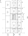
- FIG 3 is a timing diagram 300 depicting an illustrative system in Panel Self-Refresh Mode in which the sink device 150 includes adaptive synchronization, in accordance with at least one embodiment described herein.
- temporal synchronization between the source device 110 and the sink device 150 is not maintained during all or a portion of the PSR/PSR2 operating mode.
- the sink device 150 In the PSR operating mode, the sink device 150 will present image data stored locally in the frame buffer circuitry 172.
- the source device 110 and the sink device 150 will temporally resynchronize upon exiting the PSR/PSR2 operating mode.
- the source device 110 generates Frame 1 (310), Frame 2 (320), Frame 3 (330), Frame 4 (340), and Frame 5 (350) each of which may be rendered at different frame rates.
- the source device 110 communicates the respective frame to the sink device 150 via the high-bandwidth link 130.
- the sink device 150 initially presents the image data from Frame “0.” Contemporaneous with the display of Frame "0,” the sink device 150 completes the receipt of image data associated with Frame 1 (310) via the high-bandwidth communications link 130. After the minimum VB interval 260B, the sink device displays the image data associated with Frame 1 (310).
- the sink device 150 Contemporaneous with the display of Frame 1 (310), the sink device 150 completes the receipt of image data associated with Frame 2 (320) via the high-bandwidth communications link 130 and, after a minimum VB interval 260C begins displaying the image data associated with Frame 2 (320).
- Frame 3 (330) data requires an extended time to generate, consequently after waiting the maximum VB interval 260D, the sink device again displays image data associated with Frame 2 (320).
- the source control circuitry 120 may place the high-bandwidth communications link 130 in a standby or low power consumption mode.
- FIG 4 is a schematic diagram of an illustrative electronic, processor-based, device 400 that includes a graphics processing unit (“GPU")/source device 110 and an OLED display/sink device 150, in accordance with at least one embodiment described herein.
- the processor-based device 400 may additionally include one or more of the following: processor circuitry 410, a wireless input/output (I/O) interface 420, a wired I/O interface 430, system memory 440, power management circuitry 450, a non-transitory storage device 460, and a network interface 470.
- I/O input/output
- I/O wireless input/output
- wired I/O interface 430 system memory
- power management circuitry 450 power management circuitry
- non-transitory storage device 460 a non-transitory storage device 460
- network interface 470 a network interface 470.
- Example, non-limiting processor-based devices 400 may include, but are not limited to: smartphones, wearable computers, portable computing devices, handheld computing
- the processor-based device 400 includes processor circuitry 410 capable of executing machine-readable instruction sets and generating an output signal capable of providing a display output to a system user via the OLED display 150.
- processor circuitry 410 capable of executing machine-readable instruction sets and generating an output signal capable of providing a display output to a system user via the OLED display 150.
- the processor circuitry 410 may include any number of hardwired or configurable circuits, some or all of which may include programmable and/or configurable combinations of electronic components, semiconductor devices, and/or logic elements that are disposed partially or wholly in a PC, server, or other computing system capable of executing machine-readable instructions.
- the processor-based device 400 includes a bus or similar communications link 416 that communicably couples and facilitates the exchange of information and/or data between various system components including the processor circuitry 410, the source device/GPU circuitry 110, one or more wireless I/O interfaces 420, one or more wired I/O interfaces 430, the system memory 440, the power management circuitry 450, one or more storage devices 460, and/or one or more network interfaces 470.
- the processor-based device 400 may be referred to in the singular herein, but this is not intended to limit the embodiments to a single processor-based device 400, since in certain embodiments, there may be more than one processor-based device 400 that incorporates, includes, or contains any number of communicably coupled, collocated, or remote networked circuits or devices.
- the processor circuitry 410 may include any number, type, or combination of currently available or future developed devices capable of executing machine-readable instruction sets.
- the processor circuitry 410 may include but is not limited to any current or future developed single- or multi-core processor or microprocessor, such as: on or more systems on a chip (SOCs); central processing units (CPUs); digital signal processors (DSPs); graphics processing units (GPUs); application-specific integrated circuits (ASICs), programmable logic units, field programmable gate arrays (FPGAs), and the like.
- SOCs systems on a chip
- CPUs central processing units
- DSPs digital signal processors
- GPUs graphics processing units
- ASICs application-specific integrated circuits
- FPGAs field programmable gate arrays
- the system memory 440 may include read-only memory (“ROM”) 442 and random access memory (“RAM”) 446. A portion of the ROM 442 may be used to store or otherwise retain a basic input/output system (“BIOS”) 444.
- BIOS basic input/output system
- the BIOS 444 provides basic functionality to the processor-based device 400, for example by causing the processor circuitry 410 to load and/or execute one or more machine-readable instruction sets, such as the operating system instructions, and/or one or more applications.
- At least some of the one or more machine-readable instruction sets cause at least a portion of the processor circuitry 410 to provide, create, produce, transition, and/or function as a dedicated, specific, and particular machine, for example a word processing machine, a digital image acquisition machine, a media playing machine, a gaming system, a communications device, a smartphone, or similar.
- the processor-based device 400 may include at least one wireless input/output (I/O) interface 420.
- the at least one wireless I/O interface 420 may be communicably coupled to one or more physical output devices 422 (tactile devices, video displays, audio output devices, hardcopy output devices, etc.).
- the at least one wireless I/O interface 420 may communicably couple to one or more physical input devices 424 (pointing devices, touchscreens, keyboards, tactile devices, etc.).
- the at least one wireless I/O interface 420 may include any currently available or future developed wireless I/O interface.
- Example wireless I/O interfaces include, but are not limited to: BLUETOOTH®, near field communication (NFC), and similar.
- the processor-based device 400 may include one or more wired input/output (I/O) interfaces 430.
- the at least one wired I/O interface 430 may be communicably coupled to one or more physical output devices 422 (tactile devices, video displays, audio output devices, hardcopy output devices, etc.).
- the at least one wired I/O interface 430 may be communicably coupled to one or more physical input devices 424 (pointing devices, touchscreens, keyboards, tactile devices, etc.).
- the wired I/O interface 430 may include any currently available or future developed I/O interface.
- Example wired I/O interfaces include but are not limited to: universal serial bus (USB), IEEE 1394 ("FireWire”), and similar.
- the processor-based device 400 may include one or more communicably coupled, non-transitory, data storage devices 460.
- the data storage devices 460 may include one or more hard disk drives (HDDs) and/or one or more solid-state storage devices (SSDs).
- the one or more data storage devices 460 may include any current or future developed storage appliances, network storage devices, and/or systems. Non-limiting examples of such data storage devices 460 may include, but are not limited to, any current or future developed non-transitory storage appliances or devices, such as one or more magnetic storage devices, one or more optical storage devices, one or more electro-resistive storage devices, one or more molecular storage devices, one or more quantum storage devices, or various combinations thereof.
- the one or more data storage devices 460 may include one or more removable storage devices, such as one or more flash drives, flash memories, flash storage units, or similar appliances or devices capable of communicable coupling to and decoupling from the processor-based device 400.
- the one or more data storage devices 460 may include interfaces or controllers (not shown) communicatively coupling the respective storage device or system to the bus 416.
- the one or more data storage devices 460 may store, retain, or otherwise contain machine-readable instruction sets, data structures, program modules, data stores, databases, logical structures, and/or other data useful to the processor circuitry 410 and/or source device/GPU circuitry 110 and/or one or more applications executed on or by the processor circuitry 410 and/or source device/GPU circuitry 110.
- one or more data storage devices 460 may be communicably coupled to the processor circuitry 410, for example via the bus 416 or via one or more wired communications interfaces 430 (e.g., Universal Serial Bus or USB); one or more wireless communications interfaces 420 (e.g ., Bluetooth®, Near Field Communication or NFC); and/or one or more network interfaces 470 (IEEE 802.3 or Ethernet, IEEE 802.11, or WiFi®, etc. ) .
- wired communications interfaces 430 e.g., Universal Serial Bus or USB
- wireless communications interfaces 420 e.g ., Bluetooth®, Near Field Communication or NFC
- network interfaces 470 IEEE 802.3 or Ethernet, IEEE 802.11, or WiFi®, etc.
- the one or more data storage devices 460 stores all or a portion of the instructions executed, at least in part, by the processor circuitry 410.
- the one or more data storage devices 104 may store, include, or otherwise retain operating system instructions.
- the operating system instructions may include but are not limited to any version up to the latest release of: Windows® OSx®; iOS®; Android®; Linux®; and similar.
- the one or more storage devices 460 may store, include, or otherwise retain application instructions executed by the processor circuitry 410.
- Such applications may include but are not limited to: productivity software; communications software; entertainment software; audio and/or video playback software; or similar.
- the processor-based device 400 may include power management circuitry 450 that controls one or more operational aspects of the energy storage device 452.
- the energy storage device 452 may include one or more primary (i.e ., non-rechargeable) or secondary (i.e ., rechargeable) batteries or similar energy storage devices.
- the energy storage device 452 may include one or more supercapacitors or ultracapacitors.
- the power management circuitry 450 may alter, adjust, or control the flow of energy from an external power source 454 to the energy storage device 452 and/or to the processor-based device 400.
- the power source 454 may include, but is not limited to, a solar power system, a commercial electric grid, a portable generator, an external energy storage device, or any combination thereof.
- the processor circuitry 410, the storage device 460, the system memory 740, the source device/GPU circuitry 110, the wireless I/O interface 420, the wired I/O interface 430, the power management circuitry 450, and the network interface 470 are illustrated as communicatively coupled to each other via the bus 416, thereby providing connectivity between the above-described components.
- the above-described components may be communicatively coupled in a different manner than illustrated in FIG 4 .
- one or more of the above-described components may be directly coupled to other components, or may be coupled to each other, via one or more intermediary components (not shown).
- one or more of the above-described components may be integrated into the processor circuitry 410 and/or the graphics processor circuitry 412.
- all or a portion of the bus 416 may be omitted and the components are coupled directly to each other using suitable wired or wireless connections.
- FIG 5 is a high-level block flow diagram of an illustrative method 500 that communicatively couples a source device 110 having Panel Self-Refresh (PSR/PSR2) equipped source control circuitry 120 with a sink device 150 having adaptive synchronization equipped sink control circuitry 160, in accordance with at least one embodiment described herein.
- the method 500 commences at 502.
- the graphics circuitry 112 disposed in the source device 110 generates a plurality of frames 132A-132n.
- each of the frames 132 may have the same or a different frame generation rate.
- the source control circuitry 120 causes the graphics circuitry 112 to transfer the frames 132A-132n to the high-bandwidth transmitter circuit 114 for transmission, via the high-bandwidth communications link 130, to the high-bandwidth receiver circuit 154 in the sink device 150.
- the sink control circuitry 160 attempts to synchronize the frame refresh rate of a display device 152, such as an OLED display, to the frame generation rate of the source device 110.
- the source control circuitry 120 places the system into a Panel Self Refresh (PSR/PSR2) operating mode in response to detecting unchanging (PSR) or minimally changing (PSR2) image data included in each of a plurality of frames generated by the graphics circuitry 112.
- PSR/PSR2 operating mode the high-bandwidth transmitter circuit 114, the high-bandwidth receiver circuit 154, and the high-bandwidth communications link 130 may be placed in a standby or similar low-power consumption mode.
- the high-bandwidth communications link 130 is placed in standby mode, temporal synchronization between the source control circuitry 120 and the sink control circuitry 160 via the high-bandwidth communications link 130 may be impacted or even interrupted completely.
- the sink control circuitry 160 in response to entering the PSR/PSR2 operating mode, causes a storage of at least one frame in the frame buffer circuitry 172 disposed in the sink device 150.
- the sink control circuitry 160 will continue to display the image stored in the frame buffer circuitry 172 for at least a portion of the duration of the PSR/PSR2 operating mode.
- the source control circuitry 120 and/or the sink control circuitry 160 temporally synchronize the source device 110 and the sink device 150 in response to exiting the PSR/PSR2 operating mode.
- the source device 110 and the sink device 150 may maintain temporal synchronization contemporaneous with all or a portion of the PSR/PSR2 operating mode.
- the source device 110 and the sink device 150 may lose temporal synchronization during at least a portion of the PSR/PSR2 operating mode and may re-synchronize after exiting the PSR/PSR2 operating mode.
- the sink control circuitry 160 adjusts the refresh rate of the communicatively coupled display device 152 based, at least in part, on the frame generation rate of the source device 110.
- the method 500 concludes at 516.
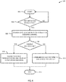
- FIG 6 is a high-level flow diagram of an illustrative method 600 of maintaining temporal synchronization between a source device 110 and a sink device 150 contemporaneous with at least a portion of the PSR/PSR2 operating mode, in accordance with at least one embodiment described herein.
- the method 600 may be used in conjunction with the method 500 depicted in FIG 5 .
- the method 600 commences at 602.
- the source control circuitry 120 and/or the sink control circuitry 160 determines whether the system has been placed in the PSR/PSR2 operating mode. Responsive to a determination that the system has not been placed in PSR/PSR2 operating mode, the method 600 returns to 602.
- the source control circuitry 120 and/or the sink control circuitry 160 may communicate synchronization signals via one or more sideband channels.
- the source control circuitry 120 and/or the sink control circuitry 160 may establish a sideband connection via the side-channel transceiver circuitry 116, the side-channel transceiver circuitry 156, and the low bandwidth communications link 140.
- the source control circuitry 120 determines whether to place the high-bandwidth communications link 130 in a standby or low power consumption mode. Responsive to a determination that the high-bandwidth communications link 130 should be placed in a standby or low power consumption mode, the method 600 continues at 610. Responsive to a determination that the high-bandwidth communications link 130 should not be placed in a standby or low power consumption mode, the method 600 continues at 612.
- the source control circuitry 120 places the high-bandwidth communications link 130 in a standby or low power consumption mode.
- the method 600 concludes at 614.
- the source control circuitry 120 maintains the high-bandwidth communications link 130 and generates an idle pattern image for transmission to the sink device 150.
- the method 600 concludes at 614.
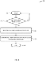
- FIG 7 is a high-level flow diagram of an illustrative method 700 of maintaining temporal synchronization between a source device 110 and a sink device 150 contemporaneous with at least a portion of the PSR/PSR2 operating mode, in accordance with at least one embodiment described herein.
- the method 700 may be used in conjunction with the method 500 depicted in FIG 5 .
- the method 700 commences at 702.
- the source control circuitry 120 and/or the sink control circuitry 160 determines whether the system has been placed in the PSR/PSR2 operating mode. Responsive to a determination that the system has not been placed in PSR/PSR2 operating mode, the method 700 returns to 702.
- the source control circuitry 120 and/or the sink control circuitry 160 may communicate synchronization signals via one or more sideband channels, such as via bidirectional FS HDP.
- the source control circuitry 120 determines whether to place the high-bandwidth communications link 130 in a standby or low power consumption mode. Responsive to a determination that the high-bandwidth communications link 130 should be placed in a standby or low power consumption mode, the method 700 continues at 710. Responsive to a determination that the high-bandwidth communications link 130 should not be placed in a standby or low power consumption mode, the method 700 continues at 712.
- the source control circuitry 120 places the high-bandwidth communications link 130 in a standby or low power consumption mode.
- the method 700 concludes at 714.
- the source control circuitry 120 maintains the high-bandwidth communications link 130 and generates an idle pattern image for transmission to the sink device 150.
- the method 700 concludes at 714.
- FIG 8 is a high-level flow diagram of an illustrative method 800 of maintaining temporal synchronization between a source device 110 and a sink device 150 contemporaneous with at least a portion of the PSR/PSR2 operating mode, in accordance with at least one embodiment described herein.
- the method 800 may be used in conjunction with the method 500 depicted in FIG 5 .
- the method 800 commences at 802.
- the source control circuitry 120 and/or the sink control circuitry 160 determines whether the system has been placed in the PSR/PSR2 operating mode. Responsive to a determination that the system has not been placed in PSR/PSR2 operating mode, the method 800 returns to 802. Responsive to a determination that the system has been placed in PSR/PSR2 operating mode, the method 800 continues to 806.
- the source control circuitry 120 maintains the high-bandwidth communications link 130 linking the high-bandwidth transmitter circuit 114 with the high-bandwidth receiver circuit 154.
- the source control circuitry 120 communicates timing marker data to the sink device 150 to maintain synchronization between the source device and the sink device.
- the method 800 concludes at 810.
- FIG 9 is a high-level flow diagram of an illustrative method 900 of resynchronizing a source device 110 and a sink device 150 upon exiting the PSR/PSR2 operating mode, in accordance with at least one embodiment described herein.
- the method 900 may be used in conjunction with the method 500 depicted in FIG 5 .
- the method 900 commences at 902.
- the sink control circuitry 160 determines a duration and/or an equivalent number of frames needed to resynchronize the sink device 150 upon the system exiting the PSR/PSR2 operating mode.
- the sink control circuitry 160 causes the storage of data and/or information indicative of the number of frames determined at 904 in one or more register circuits 174 included in memory circuitry local to the sink device 150.
- the source control circuitry 120 places the system in a PSR/PSR2 operating mode in which the high-bandwidth transmitter circuit 114, high-bandwidth receiver circuit 154, and high-bandwidth communications link 130 are placed in a standby or similar low power consumption operating mode.
- the source control circuitry 120 reads the data indicative of the number of frames in the one or more register circuits 174 included in memory circuitry local to the sink device 150.
- the source control circuitry 120 causes a delay equal to the number of frames received at 910.
- the method 900 concludes at 914.
- FIGs 5 , 6 , 7 , 8 , and 9 illustrate various operations according to one or more embodiments, it is to be understood that not all of the operations depicted in FIGs 5 , 6 , 7 , 8 , and 9 are necessary for other embodiments. Indeed, it is fully contemplated herein that in other embodiments of the present disclosure, the operations depicted in FIGs 5 , 6 , 7 , 8 , and 9 and/or other operations described herein, may be combined in a manner not specifically shown in any of the drawings, but still fully consistent with the present disclosure. Thus, claims directed to features and/or operations that are not exactly shown in one drawing are deemed within the scope and content of the present disclosure.
- a list of items joined by the term “and/or” can mean any combination of the listed items.
- the phrase “A, B and/or C” can mean A; B; C; A and B; A and C; B and C; or A, B and C.
- a list of items joined by the term "at least one of' can mean any combination of the listed terms.
- the phrases "at least one of A, B or C” can mean A; B; C; A and B; A and C; B and C; or A, B and C.
- system or “module” may refer to, for example, software, firmware and/or circuitry configured to perform any of the aforementioned operations.
- Software may be embodied as a software package, code, instructions, instruction sets and/or data recorded on non-transitory computer readable storage mediums.
- Firmware may be embodied as code, instructions or instruction sets and/or data that are hard-coded (e.g., nonvolatile) in memory devices.
- circuitry may comprise, for example, singly or in any combination, hardwired circuitry, programmable circuitry such as computer processors comprising one or more individual instruction processing cores, state machine circuitry, and/or firmware that stores instructions executed by programmable circuitry or future computing paradigms including, for example, massive parallelism, analog or quantum computing, hardware embodiments of accelerators such as neural net processors and non-silicon implementations of the above.
- the circuitry may, collectively or individually, be embodied as circuitry that forms part of a larger system, for example, an integrated circuit (IC), system on-chip (SoC), desktop computers, laptop computers, tablet computers, servers, smartphones, etc.
- IC integrated circuit
- SoC system on-chip
- any of the operations described herein may be implemented in a system that includes one or more mediums (e.g., non-transitory storage mediums) having stored therein, individually or in combination, instructions that when executed by one or more processors perform the methods.
- the processor may include, for example, a server CPU, a mobile device CPU, and/or other programmable circuitry. Also, it is intended that operations described herein may be distributed across a plurality of physical devices, such as processing structures at more than one different physical location.
- the storage medium may include any type of tangible medium, for example, any type of disk including hard disks, floppy disks, optical disks, compact disk read-only memories (CD-ROMs), compact disk rewritables (CD-RWs), and magneto-optical disks, semiconductor devices such as read-only memories (ROMs), random access memories (RAMs) such as dynamic and static RAMs, erasable programmable read-only memories (EPROMs), electrically erasable programmable read-only memories (EEPROMs), flash memories, Solid State Disks (SSDs), embedded multimedia cards (eMMCs), secure digital input/output (SDIO) cards, magnetic or optical cards, or any type of media suitable for storing electronic instructions.
- ROMs read-only memories
- RAMs random access memories
- EPROMs erasable programmable read-only memories
- EEPROMs electrically erasable programmable read-only memories
- flash memories Solid State Disks (SSDs), embedded multimedia cards (eMMC
- the present disclosure is directed to systems and methods of maintaining source device to sink device synchronization in systems in which the source device enters a Panel Self-Refresh (PSR/PSR2) mode and the sink device enables adaptive synchronization with the source device.
- the source device and the sink device may maintain synchronization contemporaneous with at least a portion of the PSR/PSR2 operating mode.
- a high-bandwidth communications link may be maintained between the source device and the sink device.
- synchronization between the source device and the sink device may be interrupted upon the source device entering the PSR/PSR2 operating mode and may be re-established upon the source device exiting the PSR/PSR2 operating mode.
- the following examples pertain to further embodiments.
- the following examples of the present disclosure may comprise subject material such as at least one device, a method, at least one machine-readable medium for storing instructions that when executed cause a machine to perform acts based on the method, means for performing acts based on the method and/or a system for maintaining source device to sink device synchronization in systems in which the source device enters a Panel Self-Refresh (PSR/PSR2) mode and the sink device enables adaptive synchronization with the source device.
- PSR/PSR2 Panel Self-Refresh
- a data transmission system may include: a source device comprising: high-bandwidth transmitter circuitry; sideband transceiver circuitry; control circuitry to: generate a plurality of frames at one or more frame generation rates; provide the plurality of frames to the high-bandwidth transmitter circuitry; disable at least the high-bandwidth transmitter circuitry responsive to entering a Panel Self-Refresh (PSR) operating mode; synchronize the source device and the sink device responsive to exiting the PSR operating mode; and adjust, by the sink device control circuitry.
- the system may additionally include: high-bandwidth receiver circuitry to receive the plurality of frames from the source device; sideband transceiver circuitry communicatively coupled to the source device sideband transceiver circuitry; memory circuitry; control circuitry to:
- a system to maintaining source device to sink device synchronization in systems in which the source device enters a Panel Self-Refresh (PSR/PSR2) mode and the sink device enables adaptive synchronization with the source device, the system being arranged to perform the method of any of examples 16 through 29.
- PSR/PSR2 Panel Self-Refresh
- example 60 there is provided a chipset arranged to perform the method of any of examples 16 through 29.
- At least one machine readable medium comprising a plurality of instructions that, in response to be being executed on a computing device, cause the computing device to carry out the method according to any of examples 16 through 29.
- a device configured to maintaining source device to sink device synchronization in systems in which the source device enters a Panel Self-Refresh (PSR/PSR2) mode and the sink device enables adaptive synchronization with the source device, the device being arranged to perform the method of any of examples 16 through 29.
- PSR/PSR2 Panel Self-Refresh
- various embodiments may be implemented using hardware elements, software elements, or any combination thereof.
- hardware elements may include processors, microprocessors, circuits, circuit elements (e.g., transistors, resistors, capacitors, inductors, and so forth), integrated circuits, application specific integrated circuits (ASIC), programmable logic devices (PLD), digital signal processors (DSP), field programmable gate array (FPGA), logic gates, registers, semiconductor device, chips, microchips, chip sets, and so forth.
Landscapes
- Engineering & Computer Science (AREA)
- Theoretical Computer Science (AREA)
- Physics & Mathematics (AREA)
- General Physics & Mathematics (AREA)
- Computer Hardware Design (AREA)
- General Engineering & Computer Science (AREA)
- Control Of Indicators Other Than Cathode Ray Tubes (AREA)
- Controls And Circuits For Display Device (AREA)
- Liquid Crystal Display Device Control (AREA)
Priority Applications (1)
| Application Number | Priority Date | Filing Date | Title |
|---|---|---|---|
| EP21217055.9A EP4002345A1 (de) | 2019-06-28 | 2020-03-20 | Systeme und verfahren zur selbstaktualisierung und adaptiven synchronisation von kombinierten tafeln |
Applications Claiming Priority (1)
| Application Number | Priority Date | Filing Date | Title |
|---|---|---|---|
| US16/457,723 US11062674B2 (en) | 2019-06-28 | 2019-06-28 | Combined panel self-refresh (PSR) and adaptive synchronization systems and methods |
Related Child Applications (2)
| Application Number | Title | Priority Date | Filing Date |
|---|---|---|---|
| EP21217055.9A Division-Into EP4002345A1 (de) | 2019-06-28 | 2020-03-20 | Systeme und verfahren zur selbstaktualisierung und adaptiven synchronisation von kombinierten tafeln |
| EP21217055.9A Division EP4002345A1 (de) | 2019-06-28 | 2020-03-20 | Systeme und verfahren zur selbstaktualisierung und adaptiven synchronisation von kombinierten tafeln |
Publications (2)
| Publication Number | Publication Date |
|---|---|
| EP3757983A1 true EP3757983A1 (de) | 2020-12-30 |
| EP3757983B1 EP3757983B1 (de) | 2024-10-16 |
Family
ID=68238148
Family Applications (2)
| Application Number | Title | Priority Date | Filing Date |
|---|---|---|---|
| EP20164435.8A Active EP3757983B1 (de) | 2019-06-28 | 2020-03-20 | Systeme und verfahren zur selbstaktualisierung und adaptiven synchronisation von kombinierten tafeln |
| EP21217055.9A Pending EP4002345A1 (de) | 2019-06-28 | 2020-03-20 | Systeme und verfahren zur selbstaktualisierung und adaptiven synchronisation von kombinierten tafeln |
Family Applications After (1)
| Application Number | Title | Priority Date | Filing Date |
|---|---|---|---|
| EP21217055.9A Pending EP4002345A1 (de) | 2019-06-28 | 2020-03-20 | Systeme und verfahren zur selbstaktualisierung und adaptiven synchronisation von kombinierten tafeln |
Country Status (3)
| Country | Link |
|---|---|
| US (2) | US11062674B2 (de) |
| EP (2) | EP3757983B1 (de) |
| CN (2) | CN114530135B (de) |
Families Citing this family (10)
| Publication number | Priority date | Publication date | Assignee | Title |
|---|---|---|---|---|
| US10824188B2 (en) * | 2019-01-14 | 2020-11-03 | Groq, Inc. | Multichip timing synchronization circuits and methods |
| US11062674B2 (en) | 2019-06-28 | 2021-07-13 | Intel Corporation | Combined panel self-refresh (PSR) and adaptive synchronization systems and methods |
| US11025858B2 (en) * | 2019-08-08 | 2021-06-01 | Netflix, Inc. | Frame rate conversion |
| JP7341856B2 (ja) * | 2019-10-28 | 2023-09-11 | キヤノン株式会社 | 制御装置、表示装置の制御方法、プログラム、および記憶媒体 |
| WO2021096883A1 (en) * | 2019-11-15 | 2021-05-20 | Qualcomm Incorporated | Methods and apparatus for adaptive display frame scheduling |
| KR102934167B1 (ko) * | 2020-02-21 | 2026-03-04 | 퀄컴 인코포레이티드 | 지연된 그래픽 프로세싱 유닛 렌더 시간을 보상하기 위한 감소된 디스플레이 프로세싱 유닛 전달 시간 |
| US12586508B2 (en) * | 2021-12-17 | 2026-03-24 | Intel Corporation | Asynchronous display pixel data streaming over I/O connections |
| WO2024071932A1 (ko) * | 2022-09-30 | 2024-04-04 | 삼성전자주식회사 | 디스플레이 구동 회로로의 송신을 위한 전자 장치 및 방법 |
| KR20240083612A (ko) | 2022-12-05 | 2024-06-12 | 삼성전자주식회사 | 디스플레이 드라이버, 시스템 온 칩 및 이들을 포함하는 디스플레이 시스템 |
| WO2024128448A1 (ko) * | 2022-12-12 | 2024-06-20 | 삼성전자 주식회사 | 적응형 동기화 기술이 적용된 디스플레이를 갖는 전자 장치 |
Citations (2)
| Publication number | Priority date | Publication date | Assignee | Title |
|---|---|---|---|---|
| GB2489102A (en) * | 2011-03-14 | 2012-09-19 | Nvidia Corp | Method of controlling sparse refresh of a self-refreshing display device coupled to a graphics controller. |
| US20140168233A1 (en) * | 2012-12-18 | 2014-06-19 | Apple Inc. | Display panel self-refresh entry and exit |
Family Cites Families (31)
| Publication number | Priority date | Publication date | Assignee | Title |
|---|---|---|---|---|
| US20070152993A1 (en) * | 2005-12-29 | 2007-07-05 | Intel Corporation | Method, display, graphics system and computer system for power efficient displays |
| JP2011521600A (ja) * | 2008-05-26 | 2011-07-21 | コーニンクレッカ フィリップス エレクトロニクス エヌ ヴィ | マルチメディア・ソースとマルチメディア・シンクを動作モードからスタンバイ・モードへ及びスタンバイ・モードから動作モードへ切り替える方法 |
| US8704839B2 (en) * | 2010-05-26 | 2014-04-22 | Stmicroelectronics, Inc. | Video frame self-refresh in a sink device |
| US8854344B2 (en) * | 2010-12-13 | 2014-10-07 | Ati Technologies Ulc | Self-refresh panel time synchronization |
| US20120147020A1 (en) * | 2010-12-13 | 2012-06-14 | Ati Technologies Ulc | Method and apparatus for providing indication of a static frame |
| JP5679891B2 (ja) * | 2011-04-26 | 2015-03-04 | 京セラ株式会社 | 携帯電子機器、制御方法および制御プログラム |
| US8645585B2 (en) * | 2011-06-10 | 2014-02-04 | Nvidia Corporation | System and method for dynamically configuring a serial data link in a display device |
| US9165537B2 (en) * | 2011-07-18 | 2015-10-20 | Nvidia Corporation | Method and apparatus for performing burst refresh of a self-refreshing display device |
| US9196216B2 (en) * | 2011-12-07 | 2015-11-24 | Parade Technologies, Ltd. | Frame buffer management and self-refresh control in a self-refresh display system |
| JP6010917B2 (ja) | 2012-02-15 | 2016-10-19 | ヤマハ株式会社 | 電子楽器の鍵盤装置 |
| KR101307557B1 (ko) * | 2012-03-09 | 2013-09-12 | 엘지디스플레이 주식회사 | 표시장치와 그의 패널 셀프 리프레시 동작 제어방법 |
| KR101158876B1 (ko) * | 2012-03-09 | 2012-06-25 | 엘지디스플레이 주식회사 | 표시장치와 그의 패널 셀프 리프레시 동작 제어방법 |
| KR20130103859A (ko) * | 2012-03-12 | 2013-09-25 | 삼성전자주식회사 | 디스플레이 드라이버의 동작 방법 및 디스플레이 제어 시스템 |
| KR101315084B1 (ko) * | 2012-04-24 | 2013-10-15 | 주식회사 실리콘웍스 | 임베디드 디스플레이포트 시스템과 그를 위한 패널 셀프 리프레시 모드를 채용한 타이밍 컨트롤러 및 패널 셀프 리프레시 모드 제어 방법 |
| US8884977B2 (en) * | 2012-08-24 | 2014-11-11 | Analogix Semiconductor, Inc. | Panel self refreshing with changing dynamic refresh rate |
| US9153787B2 (en) | 2012-12-07 | 2015-10-06 | E-Ray Optoelectronics Technology Co., Ltd. | Electron transporting compounds and organic electroluminescent devices using the same |
| US9116639B2 (en) * | 2012-12-18 | 2015-08-25 | Apple Inc. | Maintaining synchronization during vertical blanking |
| KR102057502B1 (ko) * | 2013-03-07 | 2020-01-22 | 삼성전자주식회사 | 디스플레이 드라이브 집적회로 및 영상 표시 시스템 |
| US9620064B2 (en) * | 2013-03-13 | 2017-04-11 | Apple Inc. | Compensation methods for display brightness change associated with reduced refresh rate |
| US9612647B2 (en) * | 2013-11-08 | 2017-04-04 | Intel Corporation | Power management for a physical layer interface connecting a display panel to a display transmit engine |
| US9786255B2 (en) * | 2014-05-30 | 2017-10-10 | Nvidia Corporation | Dynamic frame repetition in a variable refresh rate system |
| US9589543B2 (en) * | 2015-03-18 | 2017-03-07 | Intel Corporation | Static frame image quality improvement for sink displays |
| KR102389572B1 (ko) * | 2015-06-17 | 2022-04-25 | 삼성디스플레이 주식회사 | 표시 시스템 및 표시 장치의 구동 방법 |
| KR102446880B1 (ko) * | 2015-08-17 | 2022-09-26 | 삼성디스플레이 주식회사 | 표시 장치 및 이의 구동 방법 |
| KR102529261B1 (ko) * | 2016-05-30 | 2023-05-09 | 삼성디스플레이 주식회사 | 표시장치 및 그의 구동방법 |
| US20180130443A1 (en) * | 2016-11-04 | 2018-05-10 | Nausheen Ansari | Techniques for managing transmission and display of a display data stream |
| KR102617564B1 (ko) * | 2017-01-17 | 2023-12-27 | 삼성디스플레이 주식회사 | 표시 장치 및 이의 동작 방법 |
| JP2018173485A (ja) * | 2017-03-31 | 2018-11-08 | 株式会社メガチップス | 画像処理装置 |
| JP2018173496A (ja) * | 2017-03-31 | 2018-11-08 | 株式会社メガチップス | 画像処理装置 |
| US10665210B2 (en) | 2017-12-29 | 2020-05-26 | Intel Corporation | Extending asynchronous frame updates with full frame and partial frame notifications |
| US11062674B2 (en) | 2019-06-28 | 2021-07-13 | Intel Corporation | Combined panel self-refresh (PSR) and adaptive synchronization systems and methods |
-
2019
- 2019-06-28 US US16/457,723 patent/US11062674B2/en not_active Expired - Fee Related
-
2020
- 2020-03-20 EP EP20164435.8A patent/EP3757983B1/de active Active
- 2020-03-20 EP EP21217055.9A patent/EP4002345A1/de active Pending
- 2020-03-27 CN CN202111665953.6A patent/CN114530135B/zh active Active
- 2020-03-27 CN CN202010231163.6A patent/CN112150981A/zh active Pending
-
2021
- 2021-07-12 US US17/373,587 patent/US11763774B2/en active Active
Patent Citations (2)
| Publication number | Priority date | Publication date | Assignee | Title |
|---|---|---|---|---|
| GB2489102A (en) * | 2011-03-14 | 2012-09-19 | Nvidia Corp | Method of controlling sparse refresh of a self-refreshing display device coupled to a graphics controller. |
| US20140168233A1 (en) * | 2012-12-18 | 2014-06-19 | Apple Inc. | Display panel self-refresh entry and exit |
Also Published As
| Publication number | Publication date |
|---|---|
| US11062674B2 (en) | 2021-07-13 |
| EP3757983B1 (de) | 2024-10-16 |
| US11763774B2 (en) | 2023-09-19 |
| CN112150981A (zh) | 2020-12-29 |
| CN114530135B (zh) | 2024-06-14 |
| CN114530135A (zh) | 2022-05-24 |
| US20220101809A1 (en) | 2022-03-31 |
| EP4002345A1 (de) | 2022-05-25 |
| US20190325844A1 (en) | 2019-10-24 |
Similar Documents
| Publication | Publication Date | Title |
|---|---|---|
| US11763774B2 (en) | Combined panel self-refresh (PSR) and adaptive synchronization systems and methods | |
| US11501733B2 (en) | Panel self-refresh (PSR) transmission of bulk data | |
| US10482048B2 (en) | Asymmetric power states on a communication link | |
| US20130279276A1 (en) | Separate microchannel voltage domains in stacked memory architecture | |
| TWI512676B (zh) | 用於顯示子系統之混和顯示圖框緩衝器 | |
| EP3172635B1 (de) | Architektur mit extrem niedriger leistungsaufnahme zur unterstützung von immer-an-pfad zum speicher | |
| TW201319798A (zh) | 於圖形子系統中進入和退出休眠模式的系統和方法 | |
| US20170010648A1 (en) | Interconnect To Communicate Information Uni-Directionally | |
| US11783883B2 (en) | Burst mode for self-refresh | |
| TWI564684B (zh) | 一般主機控制器延遲方法及設備 | |
| JP2021177367A (ja) | プロセッサアイドル時間のインテリジェント予測装置及び方法 | |
| US20230161723A1 (en) | Role detection for usb-based charging | |
| US20220057854A1 (en) | Techniques for sleep management in computer system | |
| US11783885B2 (en) | Interactive memory self-refresh control | |
| US20160378551A1 (en) | Adaptive hardware acceleration based on runtime power efficiency determinations | |
| US9891691B2 (en) | Reducing pin count requirements for implementation of interconnect idle states | |
| CN111065986B (zh) | 片上系统在低功率模式时进入或退出保持等级电压的机制 | |
| CN104813403A (zh) | 存储器感应放大器电压调制 | |
| US11443793B2 (en) | Battery life based on inhibited memory refreshes | |
| TWI470642B (zh) | 在效能增強模式下由串列式快閃記憶體與記憶體控制器執行的方法 | |
| US20240134440A1 (en) | Multi-core processor frequency limit determination | |
| CN205827396U (zh) | 一种增强型统一读写器 | |
| US20150378418A1 (en) | Systems and methods for conserving power in a universal serial bus (usb) | |
| US20250211009A1 (en) | Identification of charger plug | |
| US20200411079A1 (en) | High bandwidth destructive read embedded memory |
Legal Events
| Date | Code | Title | Description |
|---|---|---|---|
| PUAI | Public reference made under article 153(3) epc to a published international application that has entered the european phase |
Free format text: ORIGINAL CODE: 0009012 |
|
| STAA | Information on the status of an ep patent application or granted ep patent |
Free format text: STATUS: THE APPLICATION HAS BEEN PUBLISHED |
|
| AK | Designated contracting states |
Kind code of ref document: A1 Designated state(s): AL AT BE BG CH CY CZ DE DK EE ES FI FR GB GR HR HU IE IS IT LI LT LU LV MC MK MT NL NO PL PT RO RS SE SI SK SM TR |
|
| AX | Request for extension of the european patent |
Extension state: BA ME |
|
| STAA | Information on the status of an ep patent application or granted ep patent |
Free format text: STATUS: REQUEST FOR EXAMINATION WAS MADE |
|
| 17P | Request for examination filed |
Effective date: 20210623 |
|
| RBV | Designated contracting states (corrected) |
Designated state(s): AL AT BE BG CH CY CZ DE DK EE ES FI FR GB GR HR HU IE IS IT LI LT LU LV MC MK MT NL NO PL PT RO RS SE SI SK SM TR |
|
| STAA | Information on the status of an ep patent application or granted ep patent |
Free format text: STATUS: EXAMINATION IS IN PROGRESS |
|
| 17Q | First examination report despatched |
Effective date: 20221215 |
|
| GRAP | Despatch of communication of intention to grant a patent |
Free format text: ORIGINAL CODE: EPIDOSNIGR1 |
|
| STAA | Information on the status of an ep patent application or granted ep patent |
Free format text: STATUS: GRANT OF PATENT IS INTENDED |
|
| INTG | Intention to grant announced |
Effective date: 20240523 |
|
| GRAS | Grant fee paid |
Free format text: ORIGINAL CODE: EPIDOSNIGR3 |
|
| GRAA | (expected) grant |
Free format text: ORIGINAL CODE: 0009210 |
|
| STAA | Information on the status of an ep patent application or granted ep patent |
Free format text: STATUS: THE PATENT HAS BEEN GRANTED |
|
| AK | Designated contracting states |
Kind code of ref document: B1 Designated state(s): AL AT BE BG CH CY CZ DE DK EE ES FI FR GB GR HR HU IE IS IT LI LT LU LV MC MK MT NL NO PL PT RO RS SE SI SK SM TR |
|
| REG | Reference to a national code |
Ref country code: GB Ref legal event code: FG4D |
|
| REG | Reference to a national code |
Ref country code: CH Ref legal event code: EP |
|
| REG | Reference to a national code |
Ref country code: IE Ref legal event code: FG4D |
|
| REG | Reference to a national code |
Ref country code: DE Ref legal event code: R096 Ref document number: 602020039418 Country of ref document: DE |
|
| P01 | Opt-out of the competence of the unified patent court (upc) registered |
Free format text: CASE NUMBER: APP_54721/2024 Effective date: 20241004 |
|
| REG | Reference to a national code |
Ref country code: NL Ref legal event code: FP |
|
| REG | Reference to a national code |
Ref country code: LT Ref legal event code: MG9D |
|
| REG | Reference to a national code |
Ref country code: AT Ref legal event code: MK05 Ref document number: 1733595 Country of ref document: AT Kind code of ref document: T Effective date: 20241016 |
|
| PG25 | Lapsed in a contracting state [announced via postgrant information from national office to epo] |
Ref country code: HR Free format text: LAPSE BECAUSE OF FAILURE TO SUBMIT A TRANSLATION OF THE DESCRIPTION OR TO PAY THE FEE WITHIN THE PRESCRIBED TIME-LIMIT Effective date: 20241016 Ref country code: IS Free format text: LAPSE BECAUSE OF FAILURE TO SUBMIT A TRANSLATION OF THE DESCRIPTION OR TO PAY THE FEE WITHIN THE PRESCRIBED TIME-LIMIT Effective date: 20250216 Ref country code: PT Free format text: LAPSE BECAUSE OF FAILURE TO SUBMIT A TRANSLATION OF THE DESCRIPTION OR TO PAY THE FEE WITHIN THE PRESCRIBED TIME-LIMIT Effective date: 20250217 |
|
| PG25 | Lapsed in a contracting state [announced via postgrant information from national office to epo] |
Ref country code: FI Free format text: LAPSE BECAUSE OF FAILURE TO SUBMIT A TRANSLATION OF THE DESCRIPTION OR TO PAY THE FEE WITHIN THE PRESCRIBED TIME-LIMIT Effective date: 20241016 |
|
| PG25 | Lapsed in a contracting state [announced via postgrant information from national office to epo] |
Ref country code: BG Free format text: LAPSE BECAUSE OF FAILURE TO SUBMIT A TRANSLATION OF THE DESCRIPTION OR TO PAY THE FEE WITHIN THE PRESCRIBED TIME-LIMIT Effective date: 20241016 |
|
| PG25 | Lapsed in a contracting state [announced via postgrant information from national office to epo] |
Ref country code: ES Free format text: LAPSE BECAUSE OF FAILURE TO SUBMIT A TRANSLATION OF THE DESCRIPTION OR TO PAY THE FEE WITHIN THE PRESCRIBED TIME-LIMIT Effective date: 20241016 |
|
| PG25 | Lapsed in a contracting state [announced via postgrant information from national office to epo] |
Ref country code: NO Free format text: LAPSE BECAUSE OF FAILURE TO SUBMIT A TRANSLATION OF THE DESCRIPTION OR TO PAY THE FEE WITHIN THE PRESCRIBED TIME-LIMIT Effective date: 20250116 |
|
| PG25 | Lapsed in a contracting state [announced via postgrant information from national office to epo] |
Ref country code: LV Free format text: LAPSE BECAUSE OF FAILURE TO SUBMIT A TRANSLATION OF THE DESCRIPTION OR TO PAY THE FEE WITHIN THE PRESCRIBED TIME-LIMIT Effective date: 20241016 Ref country code: AT Free format text: LAPSE BECAUSE OF FAILURE TO SUBMIT A TRANSLATION OF THE DESCRIPTION OR TO PAY THE FEE WITHIN THE PRESCRIBED TIME-LIMIT Effective date: 20241016 Ref country code: GR Free format text: LAPSE BECAUSE OF FAILURE TO SUBMIT A TRANSLATION OF THE DESCRIPTION OR TO PAY THE FEE WITHIN THE PRESCRIBED TIME-LIMIT Effective date: 20250117 |
|
| PG25 | Lapsed in a contracting state [announced via postgrant information from national office to epo] |
Ref country code: PL Free format text: LAPSE BECAUSE OF FAILURE TO SUBMIT A TRANSLATION OF THE DESCRIPTION OR TO PAY THE FEE WITHIN THE PRESCRIBED TIME-LIMIT Effective date: 20241016 |
|
| PG25 | Lapsed in a contracting state [announced via postgrant information from national office to epo] |
Ref country code: RS Free format text: LAPSE BECAUSE OF FAILURE TO SUBMIT A TRANSLATION OF THE DESCRIPTION OR TO PAY THE FEE WITHIN THE PRESCRIBED TIME-LIMIT Effective date: 20250116 |
|
| PG25 | Lapsed in a contracting state [announced via postgrant information from national office to epo] |
Ref country code: SM Free format text: LAPSE BECAUSE OF FAILURE TO SUBMIT A TRANSLATION OF THE DESCRIPTION OR TO PAY THE FEE WITHIN THE PRESCRIBED TIME-LIMIT Effective date: 20241016 |
|
| PG25 | Lapsed in a contracting state [announced via postgrant information from national office to epo] |
Ref country code: DK Free format text: LAPSE BECAUSE OF FAILURE TO SUBMIT A TRANSLATION OF THE DESCRIPTION OR TO PAY THE FEE WITHIN THE PRESCRIBED TIME-LIMIT Effective date: 20241016 |
|
| REG | Reference to a national code |
Ref country code: DE Ref legal event code: R097 Ref document number: 602020039418 Country of ref document: DE |
|
| PG25 | Lapsed in a contracting state [announced via postgrant information from national office to epo] |
Ref country code: EE Free format text: LAPSE BECAUSE OF FAILURE TO SUBMIT A TRANSLATION OF THE DESCRIPTION OR TO PAY THE FEE WITHIN THE PRESCRIBED TIME-LIMIT Effective date: 20241016 |
|
| PG25 | Lapsed in a contracting state [announced via postgrant information from national office to epo] |
Ref country code: RO Free format text: LAPSE BECAUSE OF FAILURE TO SUBMIT A TRANSLATION OF THE DESCRIPTION OR TO PAY THE FEE WITHIN THE PRESCRIBED TIME-LIMIT Effective date: 20241016 |
|
| PG25 | Lapsed in a contracting state [announced via postgrant information from national office to epo] |
Ref country code: SK Free format text: LAPSE BECAUSE OF FAILURE TO SUBMIT A TRANSLATION OF THE DESCRIPTION OR TO PAY THE FEE WITHIN THE PRESCRIBED TIME-LIMIT Effective date: 20241016 |
|
| PG25 | Lapsed in a contracting state [announced via postgrant information from national office to epo] |
Ref country code: CZ Free format text: LAPSE BECAUSE OF FAILURE TO SUBMIT A TRANSLATION OF THE DESCRIPTION OR TO PAY THE FEE WITHIN THE PRESCRIBED TIME-LIMIT Effective date: 20241016 |
|
| PG25 | Lapsed in a contracting state [announced via postgrant information from national office to epo] |
Ref country code: IT Free format text: LAPSE BECAUSE OF FAILURE TO SUBMIT A TRANSLATION OF THE DESCRIPTION OR TO PAY THE FEE WITHIN THE PRESCRIBED TIME-LIMIT Effective date: 20241016 |
|
| PLBE | No opposition filed within time limit |
Free format text: ORIGINAL CODE: 0009261 |
|
| STAA | Information on the status of an ep patent application or granted ep patent |
Free format text: STATUS: NO OPPOSITION FILED WITHIN TIME LIMIT |
|
| PG25 | Lapsed in a contracting state [announced via postgrant information from national office to epo] |
Ref country code: SE Free format text: LAPSE BECAUSE OF FAILURE TO SUBMIT A TRANSLATION OF THE DESCRIPTION OR TO PAY THE FEE WITHIN THE PRESCRIBED TIME-LIMIT Effective date: 20241016 |
|
| 26N | No opposition filed |
Effective date: 20250717 |
|
| PG25 | Lapsed in a contracting state [announced via postgrant information from national office to epo] |
Ref country code: MC Free format text: LAPSE BECAUSE OF FAILURE TO SUBMIT A TRANSLATION OF THE DESCRIPTION OR TO PAY THE FEE WITHIN THE PRESCRIBED TIME-LIMIT Effective date: 20241016 |
|
| REG | Reference to a national code |
Ref country code: CH Ref legal event code: H13 Free format text: ST27 STATUS EVENT CODE: U-0-0-H10-H13 (AS PROVIDED BY THE NATIONAL OFFICE) Effective date: 20251023 |
|
| PG25 | Lapsed in a contracting state [announced via postgrant information from national office to epo] |
Ref country code: LU Free format text: LAPSE BECAUSE OF NON-PAYMENT OF DUE FEES Effective date: 20250320 |
|
| REG | Reference to a national code |
Ref country code: BE Ref legal event code: MM Effective date: 20250331 |
|
| PG25 | Lapsed in a contracting state [announced via postgrant information from national office to epo] |
Ref country code: BE Free format text: LAPSE BECAUSE OF NON-PAYMENT OF DUE FEES Effective date: 20250331 |
|
| PG25 | Lapsed in a contracting state [announced via postgrant information from national office to epo] |
Ref country code: CH Free format text: LAPSE BECAUSE OF NON-PAYMENT OF DUE FEES Effective date: 20250331 |
|
| PG25 | Lapsed in a contracting state [announced via postgrant information from national office to epo] |
Ref country code: IE Free format text: LAPSE BECAUSE OF NON-PAYMENT OF DUE FEES Effective date: 20250320 |
|
| PGFP | Annual fee paid to national office [announced via postgrant information from national office to epo] |
Ref country code: NL Payment date: 20260227 Year of fee payment: 7 |
|
| PGFP | Annual fee paid to national office [announced via postgrant information from national office to epo] |
Ref country code: GB Payment date: 20260223 Year of fee payment: 7 |
|
| PGFP | Annual fee paid to national office [announced via postgrant information from national office to epo] |
Ref country code: DE Payment date: 20260102 Year of fee payment: 7 |
|
| PGFP | Annual fee paid to national office [announced via postgrant information from national office to epo] |
Ref country code: FR Payment date: 20260223 Year of fee payment: 7 |