EP3748705B1 - Struktur einer speichervorrichtung und herstellungsverfahren dafür - Google Patents
Struktur einer speichervorrichtung und herstellungsverfahren dafür Download PDFInfo
- Publication number
- EP3748705B1 EP3748705B1 EP20173807.7A EP20173807A EP3748705B1 EP 3748705 B1 EP3748705 B1 EP 3748705B1 EP 20173807 A EP20173807 A EP 20173807A EP 3748705 B1 EP3748705 B1 EP 3748705B1
- Authority
- EP
- European Patent Office
- Prior art keywords
- layer
- memory device
- resistive
- substrate
- bottom electrode
- Prior art date
- Legal status (The legal status is an assumption and is not a legal conclusion. Google has not performed a legal analysis and makes no representation as to the accuracy of the status listed.)
- Active
Links
Images



Classifications
-
- H—ELECTRICITY
- H10—SEMICONDUCTOR DEVICES; ELECTRIC SOLID-STATE DEVICES NOT OTHERWISE PROVIDED FOR
- H10N—ELECTRIC SOLID-STATE DEVICES NOT OTHERWISE PROVIDED FOR
- H10N70/00—Solid-state devices having no potential barriers, and specially adapted for rectifying, amplifying, oscillating or switching
- H10N70/20—Multistable switching devices, e.g. memristors
- H10N70/24—Multistable switching devices, e.g. memristors based on migration or redistribution of ionic species, e.g. anions, vacancies
-
- H—ELECTRICITY
- H10—SEMICONDUCTOR DEVICES; ELECTRIC SOLID-STATE DEVICES NOT OTHERWISE PROVIDED FOR
- H10B—ELECTRONIC MEMORY DEVICES
- H10B63/00—Resistance change memory devices, e.g. resistive RAM [ReRAM] devices
- H10B63/80—Arrangements comprising multiple bistable or multi-stable switching components of the same type on a plane parallel to the substrate, e.g. cross-point arrays
-
- H—ELECTRICITY
- H10—SEMICONDUCTOR DEVICES; ELECTRIC SOLID-STATE DEVICES NOT OTHERWISE PROVIDED FOR
- H10N—ELECTRIC SOLID-STATE DEVICES NOT OTHERWISE PROVIDED FOR
- H10N70/00—Solid-state devices having no potential barriers, and specially adapted for rectifying, amplifying, oscillating or switching
- H10N70/011—Manufacture or treatment of multistable switching devices
-
- H—ELECTRICITY
- H10—SEMICONDUCTOR DEVICES; ELECTRIC SOLID-STATE DEVICES NOT OTHERWISE PROVIDED FOR
- H10N—ELECTRIC SOLID-STATE DEVICES NOT OTHERWISE PROVIDED FOR
- H10N70/00—Solid-state devices having no potential barriers, and specially adapted for rectifying, amplifying, oscillating or switching
- H10N70/011—Manufacture or treatment of multistable switching devices
- H10N70/021—Formation of switching materials, e.g. deposition of layers
-
- H—ELECTRICITY
- H10—SEMICONDUCTOR DEVICES; ELECTRIC SOLID-STATE DEVICES NOT OTHERWISE PROVIDED FOR
- H10N—ELECTRIC SOLID-STATE DEVICES NOT OTHERWISE PROVIDED FOR
- H10N70/00—Solid-state devices having no potential barriers, and specially adapted for rectifying, amplifying, oscillating or switching
- H10N70/011—Manufacture or treatment of multistable switching devices
- H10N70/021—Formation of switching materials, e.g. deposition of layers
- H10N70/028—Formation of switching materials, e.g. deposition of layers by conversion of electrode material, e.g. oxidation
-
- H—ELECTRICITY
- H10—SEMICONDUCTOR DEVICES; ELECTRIC SOLID-STATE DEVICES NOT OTHERWISE PROVIDED FOR
- H10N—ELECTRIC SOLID-STATE DEVICES NOT OTHERWISE PROVIDED FOR
- H10N70/00—Solid-state devices having no potential barriers, and specially adapted for rectifying, amplifying, oscillating or switching
- H10N70/801—Constructional details of multistable switching devices
-
- H—ELECTRICITY
- H10—SEMICONDUCTOR DEVICES; ELECTRIC SOLID-STATE DEVICES NOT OTHERWISE PROVIDED FOR
- H10N—ELECTRIC SOLID-STATE DEVICES NOT OTHERWISE PROVIDED FOR
- H10N70/00—Solid-state devices having no potential barriers, and specially adapted for rectifying, amplifying, oscillating or switching
- H10N70/801—Constructional details of multistable switching devices
- H10N70/821—Device geometry
- H10N70/823—Device geometry adapted for essentially horizontal current flow, e.g. bridge type devices
-
- H—ELECTRICITY
- H10—SEMICONDUCTOR DEVICES; ELECTRIC SOLID-STATE DEVICES NOT OTHERWISE PROVIDED FOR
- H10N—ELECTRIC SOLID-STATE DEVICES NOT OTHERWISE PROVIDED FOR
- H10N70/00—Solid-state devices having no potential barriers, and specially adapted for rectifying, amplifying, oscillating or switching
- H10N70/801—Constructional details of multistable switching devices
- H10N70/821—Device geometry
- H10N70/826—Device geometry adapted for essentially vertical current flow, e.g. sandwich or pillar type devices
-
- H—ELECTRICITY
- H10—SEMICONDUCTOR DEVICES; ELECTRIC SOLID-STATE DEVICES NOT OTHERWISE PROVIDED FOR
- H10N—ELECTRIC SOLID-STATE DEVICES NOT OTHERWISE PROVIDED FOR
- H10N70/00—Solid-state devices having no potential barriers, and specially adapted for rectifying, amplifying, oscillating or switching
- H10N70/801—Constructional details of multistable switching devices
- H10N70/821—Device geometry
- H10N70/826—Device geometry adapted for essentially vertical current flow, e.g. sandwich or pillar type devices
- H10N70/8265—Device geometry adapted for essentially vertical current flow, e.g. sandwich or pillar type devices on sidewalls of dielectric structures, e.g. mesa-shaped or cup-shaped devices
-
- H—ELECTRICITY
- H10—SEMICONDUCTOR DEVICES; ELECTRIC SOLID-STATE DEVICES NOT OTHERWISE PROVIDED FOR
- H10N—ELECTRIC SOLID-STATE DEVICES NOT OTHERWISE PROVIDED FOR
- H10N70/00—Solid-state devices having no potential barriers, and specially adapted for rectifying, amplifying, oscillating or switching
- H10N70/801—Constructional details of multistable switching devices
- H10N70/841—Electrodes
-
- H—ELECTRICITY
- H10—SEMICONDUCTOR DEVICES; ELECTRIC SOLID-STATE DEVICES NOT OTHERWISE PROVIDED FOR
- H10N—ELECTRIC SOLID-STATE DEVICES NOT OTHERWISE PROVIDED FOR
- H10N70/00—Solid-state devices having no potential barriers, and specially adapted for rectifying, amplifying, oscillating or switching
- H10N70/801—Constructional details of multistable switching devices
- H10N70/881—Switching materials
- H10N70/883—Oxides or nitrides
- H10N70/8833—Binary metal oxides, e.g. TaOx
Definitions
- the present invention generally relates to a semiconductor fabrication technology, in particular, to a structure of a resistive memory device and a fabrication method thereof.
- a non-volatile memory is almost indispensable in a digital electronic product.
- Digital electronic products for example, computers, mobile phones, cameras, and video recorders, are also indispensable products in daily life. Therefore, non-volatile memories are commonly in demand.
- a structure of a memory cell of a non-volatile memory may be designed in various different ways, and a corresponding structure may be provided for a different storage manner.
- a vertical memory cell for example, a resistive memory device
- the resistive memory device may have two stable resistance values by using resistance variation characteristics of a memory material under control of an applied voltage, so as to store one-bit data.
- a fabrication process is different for a different structure of a memory cell, and an inappropriate structural design may cause difficulty in fabrication and may even easily cause a failure in fabrication of a device.
- US 2016/149125 A1 discloses a semiconductor integrated circuit device and a fabrication method thereof.
- the device includes a lower electrode, a resistive layer formed in a resistance change region on the lower electrode, an upper electrode formed on the resistive layer, and an insertion layer configured to allow a reset current path of the resistive layer, which is formed from the upper electrode to the lower electrode, to be bypassed in a direction perpendicular to or parallel to a surface of the lower electrode.
- US 2013/112935 A1 discloses a non-volatile memory element with a first metal line; a plug formed on the first metal line and connected to the first metal line; a stacked structure including a first electrode, a second electrode, and a variable resistance layer, the stacked structure being formed on a plug which is connected to the first electrode; a second metal line formed on the stacked structure and directly connected to the second electrode; and a side wall protective layer which covers the side wall of the stacked structure and has an insulating property and an oxygen barrier property, wherein part of a lower surface of the second metal line is located under an upper surface of the stacked structure.
- US 2015/221700 A1 discloses an electronic device comprising a semiconductor memory unit that includes a first vertical electrode; a first variable resistance layer surrounding the first vertical electrode; a second vertical electrode surrounding the first variable resistance; a second variable resistance layer surrounding the second vertical electrode; and a plurality of horizontal electrodes contacted with an outer side of the second variable resistance layer, wherein the plurality of horizontal electrodes are spaced apart from each other in a vertical direction.
- the present invention is directed to a structure of a memory device and a fabrication method thereof.
- the memory device is a resistive memory device, and a memory material layer extends in a vertical direction.
- the present invention provides a structure of a memory device, including a substrate.
- the substrate includes a bottom electrode layer.
- a buffer layer is disposed on the substrate, in contact with the bottom electrode layer.
- a resistive layer surrounds a whole sidewall of the buffer layer and extends upward vertically from the substrate.
- a mask layer is disposed on the buffer layer and the resistive layer.
- a noble metal layer is on the substrate and fully covers the resistive layer and the mask layer.
- a top electrode layer is disposed on the noble metal layer.
- the resistive layer includes a transition metal oxide layer.
- the buffer layer is an oxygen trap layer.
- the buffer layer includes Hf, HfOx, Ta, TaOx, NiOx, TiOx, ZrOx, or ZnOx.
- an oxygen content of the transition metal oxide layer is in a saturation state.
- a size of the resistive layer is determined by a horizontal thickness of the resistive layer and a thickness of the buffer layer.
- the noble metal layer reduces oxygen diffused into or away from the resistive layer.
- the top electrode layer is thicker than the noble metal layer and a thickness of the noble metal layer is in a range of 30 to 50 angstroms.
- the substrate in the structure of memory device, includes a base layer including an interconnection line structure therein.
- An inter-layer dielectric layer is disposed on the base layer and includes an opening.
- a through via structure is filling into a lower portion of the opening.
- the bottom electrode layer is filling into an upper portion of the opening.
- the substrate in the structure of memory device, includes a base layer including an interconnection line structure therein.
- An inter-layer dielectric layer is disposed on the base layer and includes an opening.
- a through via structure is filling into a lower portion of the opening.
- the bottom electrode layer is disposed on the inter-layer dielectric layer and above the through via structure. The noble metal layer and the bottom electrode layer are isolated at least by the resistive layer.
- the present invention provides a method for fabricating a memory device.
- the method includes providing a substrate, having a bottom electrode layer therein.
- a buffer layer and a mask layer on the buffer layer are formed on the substrate in contact with the bottom electrode layer.
- An advanced oxidation process is performed on a sidewall of the buffer layer to form a resistive layer, the resistive layer is surrounding the whole sidewall of the buffer layer and extending upward vertically from the substrate.
- a noble metal layer and a top electrode layer on the noble metal layer are formed over the substrate, fully covering the resistive layer and the mask layer; and being disposed on the substrate.
- the resistive layer includes a transition metal oxide layer.
- the buffer layer is an oxygen trap layer.
- the buffer layer includes Hf, HfOx, Ta, TaOx, NiOx, TiOx, ZrOx, or ZnOx.
- an oxygen content of the transition metal oxide layer is in a saturation state.
- a size of the resistive layer is determined by a horizontal thickness of the resistive layer and a thickness of the buffer layer.
- the noble metal layer reduces oxygen diffused into or away from the resistive layer.
- the top electrode layer is thicker than the noble metal layer and a thickness of the noble metal layer is in a range of 30 to 50 angstroms.
- the step of providing the substrate includes providing a base layer, having an interconnection line structure therein.
- An inter-layer dielectric layer is formed on the base layer, the inter-layer dielectric layer includes an opening.
- a through via structure is formed, filling into a lower portion of the opening.
- the bottom electrode layer is formed, filling into an upper portion of the opening.
- the step of providing the substrate includes providing a base layer, having an interconnection line structure therein.
- An inter-layer dielectric layer is formed on the base layer, the inter-layer dielectric layer includes an opening.
- a through via structure is formed, filling into a lower portion of the opening.
- the bottom electrode layer is formed on the inter-layer dielectric layer and above the through via structure. The noble metal layer and the bottom electrode layer are isolated at least by the resistive layer.
- the present invention is directed to a structure of a memory device and a fabrication method thereof.
- the structure of a memory device is a resistive memory cell, a bottom electrode layer may be positioned accurately, and a resistive layer is designed to extend in a vertical direction.
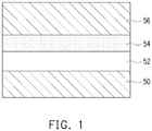
- FIG. 1 is a schematic view of a resistive storage mechanism according to an embodiment of the present invention.
- a transition metal oxide (TMO) serves as a structure of a storage mechanism.
- a TMO layer 54 for example, a Ta 2 O 5 layer, exists between a bottom electrode layer 50 and a top electrode layer 56.
- a buffer layer 52 is, for example, a TaOx layer, and serves as an oxygen trap layer. Materials of the buffer layer 52 and the TMO layer 54 will be described in detail below.
- Oxygen ions in the buffer layer 52 may be controlled to enter or leave the TMO layer 54 by biases generated by the bottom electrode layer 50 and the top electrode layer 56, to cause a change of a resistance value. Since the TMO layer 54 has two stable resistance value states, it may be used to store one-bit data.
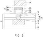
- Fig. 2 is a schematic structural view of a resistive memory device according to an embodiment of the present invention.
- the structure of a memory device includes a substrate 80.
- the substrate 80 includes a bottom electrode layer 78 therein.
- a silicon substrate 60 serves as a structural basis.
- An interconnection line structure 72 is at least formed on the silicon substrate 60 through an inter-layer dielectric layer 70 by using a semiconductor fabrication process.
- a whole including the silicon substrate 60, the inter-layer dielectric layer 70, and the interconnection line structure 72 may be referred to as a base layer.
- the present invention is not limited to a specific structure of the base layer.
- another element structure such as a transistor connected to the interconnection line structure 72, may also be formed on the silicon substrate 60.
- inter-layer dielectric layer 74 is further formed on the base layer, for example, the inter-layer dielectric layer 74 is formed on the inter-layer dielectric layer 70.
- the inter-layer dielectric layer 74 is, for example, formed of a plurality of inter-layer dielectric layers 74a and 74b, which may be, for example, a combination of oxides or nitrides.
- the inter-layer dielectric layer 74 may include other structures according to a whole actual circuit structure, and other element structures are not limited in the present invention.
- the inter-layer dielectric layer 74 also has an opening corresponding to the interconnection line structure 72.
- the through via structure 76 is only filling into a lower portion of the opening, and a bottom electrode layer 78 is additionally formed in the upper portion of the opening.
- the bottom electrode layer 78, the through via structure 76, and the interconnection line structure 72 are, for example, electrically connected.
- the through via structure 76 may also be filling into the opening, and in this way, the bottom electrode layer 78 may be formed on the inner-layer dielectric layer 74 and disposed on the through via structure 76.
- the present invention is not limited to a specific electric connection manner between the bottom electrode layer 78 and the interconnection line structure 72.
- a buffer layer 82 is disposed on the inner-layer dielectric layer 74 of the substrate 80 and in contact with the bottom electrode layer 78.
- the buffer layer 82 is, for example, an oxygen trap layer, the material of which is a material containing a transition metal or an oxide thereof, and further may be, for example, Hf, HfOx, Ta, TaOx, NiOx, TiOx, ZrOx, or ZnOx.
- the buffer layer 82 may provide oxygen ions to enter resistive layer 84 formed subsequently, or trap oxygen ions from the resistive layer 84, to change a resistance value of the resistive layer 84, thereby achieving a function of storage.
- Fig. 3 is a top schematic structural view of a buffer layer and a resistive layer of a resistive memory device according to an embodiment of the present invention.
- a geometrical shape of the buffer layer 82 is, for example, a circle or a quadrangle, but the geometrical shape of the buffer layer 82 in the present invention is not limited to the embodiment. According to the geometrical shape of the buffer layer 82, the resistive layer 84 surround the whole sidewall of the buffer layer 82.
- the resistive layer 84 is a transition metal oxide
- the material thereof may be based on the material of the buffer layer 82
- the sidewall of the resistive layer 84 is oxidized through an advanced oxidation process, and the oxidization degree is to make an oxygen content to approach to a saturation state.
- the mask layer 86 is disposed on the buffer layer 82 and the variable resistance layer 84.
- a noble metal layer 88 is disposed above the substrate 80 and fully covers the resistive layer 84 and the mark layer 86.
- the noble metal layer 88 includes, for example, Pt, Ir, Au, Pd, Ru, Os, or Re and serves as a barrier layer, to reduce oxygen diffused into or away from the resistive layer 84, so as not to influence a storage state.
- a top electrode layer 90 is disposed on the noble metal layer 88. As a whole, the top electrode layer 90 and the noble metal layer 88 form a top electrode superposed layer 92.
- another interconnection line structure 94 is also disposed on the top electrode superposed layer 92, to electrically connect the memory cell to external device part.
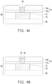
- FIGs. 4A-4G are cross-sectional schematic structural views of a fabrication process of a resistive memory device according to an embodiment of the present invention.
- the through via structure 76 has been filling into the lower portion of the opening.
- the bottom electrode layer 78 is filling into the upper portion of the opening.
- a preliminary metal layer is formed to cover the inner-layer dielectric layer 74 and filling into the upper portion of the opening.
- the portion of the preliminary metal layer on the inner-layer dielectric layer 74 is removed by using a grinding process, and the remaining metal layer is the bottom electrode layer 78, that is, the metal layer that is filling into the lower portion of the opening.
- the bottom electrode layer 78 and the through via structure 76 may be aligned accurately.
- the through via structure 76 may also be all filling into the opening.
- the bottom electrode layer 78 may be formed on the inner-layer dielectric layer 74 and is in contact with and connected to the through via structure 76.
- the present invention is not limited to a specific electric connection manner between the bottom electrode layer 78 and the interconnection line structure 72.
- the preliminary buffer layer 82 and the mask layer 86 are superposed on the inner-layer dielectric layer 74, that is, formed on the substrate 80.
- the preliminary buffer layer 82 and the mark layer 86 are defined to have a needed size, and the shape is, for example, shown in the embodiment in Fig. 3 .
- the top of the buffer layer 82 is protected by the mark layer 86, and then, the sidewall of the buffer layer 82 is further oxidized through the advanced oxidation process, so that the oxidization degree is substantially to make an oxygen content in a saturation state.
- the resistive layer 84 such as a TMO layer, is obtained after oxidation.
- the top electrode superposed layer 92 is formed on the substrate 80 and covers the resistive layer 84 and the mask layer 86. Since a change of an oxygen content of the resistive layer 84 will cause a change of a resistance value thereof, and then causes an error in stored data, the top electrode superposed layer 92 includes a common top electrode layer 90 and further includes a noble metal layer 88.
- the noble metal layer 88 may be used to reduce oxygen diffused into or away from the resistive layer 84.
- a thickness of the noble metal layer is, for example, in a range of 30 to 50 angstroms. That is to say, the top electrode layer 90 is thicker than the noble metal layer.
- the material of the noble metal layer 88 may be, for example, Pt, Ir, Au, Pd, Ru, Os, or Re.
- the materials of the top electrode layer 90 and the bottom electrode layer 78 do not need to be specifically defined.
- the metal composition of the top electrode layer 90 and the bottom electrode layer 78 may be the same as the metal composition of the buffer layer 82.
- the buffer layer 82 is, for example, a TaO x layer, and then, for example, the top electrode layer 90 and the bottom electrode layer 78 may be TaN layers.
- the top electrode superposed layer 92 is further defined to have an actual size. Subsequently, the following interconnection line structure 94 may be formed on the top electrode superposed layer 92 and fabricated according to an actually needed structure.
- the interconnection line structure 94 of the present invention is not limited to a specific structure, and the fabrication process may follow a common manner and the descriptions thereof are omitted herein.
- the quality of the resistive layer 84 may determine storage performance. A larger volume of the resistive layer 84 may be advantageous to separate the state of resistance value.
- the size of the resistive layer 84 in the present invention may be adjusted in various manners.
- Fig. 5 is a schematic structural view of a resistive memory device according to an embodiment of the present invention.
- a height of the resistive layer 84 is increased by increasing a thickness of the buffer layer 82, and thus, the volume may be increased correspondingly.
- Fig. 6 is a schematic structural view of a resistive memory device according to an embodiment of the present invention.
- a horizontal thickness of the resistive layer 84 may be increased.
- the resistive layer 84 is a ring-shaped structure.
- the volume of the resistive layer 84 may also be increased by increasing a thickness of the ring.
- the volume of the ring-shaped resistive layer 84 may be adjusted by changing the thickness and/or height. An area occupied by the memory device is unchanged and a predetermined device density may be maintained.
- the buffer layer 82 is used and the resistive layer 84 is formed on the sidewall of the buffer layer 82, to fabricate the resistive memory device.
- the bottom electrode layer 78 may also be formed in the opening to be accurately connected with the through via structure.
Landscapes
- Engineering & Computer Science (AREA)
- Manufacturing & Machinery (AREA)
- Semiconductor Memories (AREA)
Claims (15)
- Struktur einer Speichervorrichtung, umfassend:ein Substrat (80), das eine untere Elektrodenschicht (78) darin enthält;eine Pufferschicht (82), die auf dem Substrat angeordnet ist; in Kontakt mit der unteren Elektrodenschicht (78);eine Widerstandsschicht (84), die eine gesamte Seitenwand der Pufferschicht (82) umgibt und sich von dem Substrat (80) vertikal nach oben erstreckt; undeine Abdeckschicht (86), die auf der Pufferschicht (82) und der Widerstandsschicht (84) angeordnet ist; wobei die Struktur der Speichervorrichtung dadurch gekennzeichnet ist, dass sie ferner umfasst:eine Edelmetallschicht (88), die auf dem Substrat (80) angeordnet ist und die Widerstandsschicht (84) und die Abdeckschicht (86) vollständig bedeckt; undeine obere Elektrodenschicht (90), die auf der Edelmetallschicht (88) angeordnet ist.
- Struktur einer Speichervorrichtung nach Anspruch 1, wobei die Widerstandsschicht eine Übergangsmetalloxidschicht umfasst.
- Struktur einer Speichervorrichtung nach Anspruch 2, wobei die Pufferschicht eine Sauerstoff-Fangschicht ist.
- Struktur einer Speichervorrichtung nach Anspruch 3, wobei die Pufferschicht Hf, HfOx, Ta, TaOx, NiOx, TiOx, ZrOx oder ZnOx umfasst.
- Struktur einer Speichervorrichtung nach Anspruch 1, wobei eine Größe der Widerstandsschicht durch eine horizontale Dicke der Widerstandsschicht und eine Dicke der Pufferschicht bestimmt wird.
- Struktur einer Speichervorrichtung nach Anspruch 1, wobei die obere Elektrodenschicht dicker ist als die Edelmetallschicht und die Dicke der Edelmetallschicht in einem Bereich von 30 bis 50 Angström liegt.
- Struktur einer Speichervorrichtung nach Anspruch 1, wobei das Substrat umfasst:eine Basisschicht, umfassend eine darin befindliche Verbindungsleitungsstruktur;eine Zwischenschicht-Dielektrische-Schicht, die auf der Basisschicht angeordnet ist und eine Öffnung aufweist;eine Durchkontaktierungsstruktur, füllend in einen unteren Abschnitt der Öffnung; unddie untere Elektrodenschicht, füllend in einen oberen Abschnitt der Öffnung.
- Struktur einer Speichervorrichtung nach Anspruch 1, wobei das Substrat umfasst:eine Basisschicht, umfassend eine darin befindliche Verbindungsleitungsstruktur;eine Zwischenschicht-Dielektrische-Schicht, die auf der Basisschicht angeordnet ist und eine Öffnung aufweist;eine Durchkontaktierungsstruktur, füllend in einen unteren Abschnitt der Öffnung; unddie untere Elektrodenschicht, die auf der Zwischenschicht-Dielektrischen-Schicht und oberhalb der Durchkontaktierungsstruktur angeordnet ist,wobei die Edelmetallschicht und die untere Elektrodenschicht wenigstens durch die Widerstandsschicht isoliert sind.
- Verfahren zur Herstellung einer Speichervorrichtung, umfassend:
Bereitstellen eines Substrats (80), das eine untere Elektrodenschicht (78) darin enthält;Ausbilden einer Pufferschicht (82) und einer Abdeckschicht (86) auf der Pufferschicht (82) über dem Substrat, in Kontakt mit der unteren Elektrodenschicht (78); undDurchführen eines fortgeschrittenen Oxidationsprozesses an einer Seitenwand der Pufferschicht (82), um eine Widerstandsschicht (84) zu bilden, wobei die Widerstandsschicht die gesamte Seitenwand der Pufferschicht umgibt und sich von dem Substrat aus vertikal nach oben erstreckt; wobei das Verfahren dadurch gekennzeichnet ist, dass es ferner umfasstAusbilden einer Edelmetallschicht (88) und einer oberen Elektrodenschicht (90) auf der Edelmetallschicht über dem Substrat, wobei die Widerstandsschicht (84) und die Abdeckschicht (86) vollständig bedeckt werden und auf dem Substrat angeordnet sind. - Verfahren zur Herstellung einer Speichervorrichtung nach Anspruch 9, wobei die Widerstandsschicht eine Übergangsmetalloxidschicht umfasst.
- Verfahren zur Herstellung einer Speichervorrichtung nach Anspruch 9, wobei die Pufferschicht eine Sauerstoff-Fangschicht ist.
- Verfahren zur Herstellung einer Speichervorrichtung nach Anspruch 11, wobei die Pufferschicht Hf, HfOx, Ta, TaOx, NiOx, TiOx, ZrOx oder ZnOx umfasst.
- Verfahren zur Herstellung einer Speichervorrichtung nach Anspruch 9, wobei die obere Elektrodenschicht dicker ist als die Edelmetallschicht und eine Dicke der Edelmetallschicht in einem Bereich von 30 bis 50 Angström liegt.
- Verfahren zum Herstellen einer Speichervorrichtung nach Anspruch 9, wobei der Schritt des Bereitstellens des Substrats umfasst:Bereitstellen einer Basisschicht, umfassend eine darin befindliche Verbindungsleitungs struktur;Ausbilden einer Zwischenschicht-Dielektrischen-Schicht auf der Basisschicht, wobei die Zwischenschicht-Dielektrische-Schicht eine Öffnung aufweist;Ausbilden einer Durchkontaktierungsstruktur, füllend in einen unteren Abschnitt der Öffnung; undAusbilden der unteren Elektrodenschicht, füllend in einen oberen Abschnitt der Öffnung.
- Verfahren zum Herstellen einer Speichervorrichtung nach Anspruch 9, wobei der Schritt des Bereitstellens des Substrats umfasst:Bereitstellen einer Basisschicht, umfassend eine darin befindliche Verbindungsleitungsstruktur;Ausbilden einer Zwischenschicht-Dielektrische-Schicht auf der Basisschicht, wobei die Zwischenschicht-Dielektrische-Schicht eine Öffnung aufweist;Ausbilden einer Durchkontaktierungsstruktur, füllend in einen unteren Abschnitt der Öffnung; undAusbilden der unteren Elektrodenschicht, die auf der Zwischenschicht-Dielektrischen-Schicht und oberhalb der Durchkontaktierungsstruktur angeordnet ist,wobei die Edelmetallschicht und die untere Elektrodenschicht wenigstens durch die Widerstandsschicht isoliert sind.
Applications Claiming Priority (1)
| Application Number | Priority Date | Filing Date | Title |
|---|---|---|---|
| CN201910484945.8A CN112054117B (zh) | 2019-06-05 | 2019-06-05 | 存储器元件的结构及其制造方法 |
Publications (2)
| Publication Number | Publication Date |
|---|---|
| EP3748705A1 EP3748705A1 (de) | 2020-12-09 |
| EP3748705B1 true EP3748705B1 (de) | 2022-03-16 |
Family
ID=70680342
Family Applications (1)
| Application Number | Title | Priority Date | Filing Date |
|---|---|---|---|
| EP20173807.7A Active EP3748705B1 (de) | 2019-06-05 | 2020-05-11 | Struktur einer speichervorrichtung und herstellungsverfahren dafür |
Country Status (3)
| Country | Link |
|---|---|
| US (2) | US11239419B2 (de) |
| EP (1) | EP3748705B1 (de) |
| CN (1) | CN112054117B (de) |
Families Citing this family (2)
| Publication number | Priority date | Publication date | Assignee | Title |
|---|---|---|---|---|
| CN112018237B (zh) * | 2020-07-31 | 2021-11-23 | 厦门半导体工业技术研发有限公司 | 半导体器件和半导体器件的制造方法 |
| US11844291B2 (en) | 2021-06-21 | 2023-12-12 | United Microelectronics Corp. | Semiconductor memory device and fabrication method thereof |
Family Cites Families (14)
| Publication number | Priority date | Publication date | Assignee | Title |
|---|---|---|---|---|
| WO2003032392A2 (en) * | 2001-10-09 | 2003-04-17 | Axon Technologies Corporation | Programmable microelectronic device, structure, and system, and method of forming the same |
| WO2007102483A1 (ja) * | 2006-03-08 | 2007-09-13 | Matsushita Electric Industrial Co., Ltd. | 不揮発性記憶素子、不揮発記憶装置、及びそれらの製造方法 |
| KR101159075B1 (ko) * | 2006-06-27 | 2012-06-25 | 삼성전자주식회사 | n+ 계면층을 구비한 가변 저항 랜덤 액세스 메모리 소자 |
| US7981760B2 (en) * | 2008-05-08 | 2011-07-19 | Panasonic Corporation | Method for manufacturing nonvolatile storage element and method for manufacturing nonvolatile storage device |
| JP5457961B2 (ja) * | 2010-07-16 | 2014-04-02 | 株式会社東芝 | 半導体記憶装置 |
| WO2012063495A1 (ja) * | 2010-11-12 | 2012-05-18 | パナソニック株式会社 | 不揮発性半導体記憶素子の製造方法 |
| JP5442876B2 (ja) * | 2010-12-03 | 2014-03-12 | パナソニック株式会社 | 不揮発性記憶素子ならびに不揮発性記憶装置及びそれらの製造方法 |
| US20140175371A1 (en) * | 2012-12-21 | 2014-06-26 | Elijah V. Karpov | Vertical cross-point embedded memory architecture for metal-conductive oxide-metal (mcom) memory elements |
| US9178143B2 (en) * | 2013-07-29 | 2015-11-03 | Industrial Technology Research Institute | Resistive memory structure |
| KR102008365B1 (ko) * | 2014-02-03 | 2019-08-07 | 에스케이하이닉스 주식회사 | 전자 장치 |
| KR20160063067A (ko) * | 2014-11-26 | 2016-06-03 | 에스케이하이닉스 주식회사 | 저항 메모리 소자 및 그 제조 방법 |
| US9859335B1 (en) | 2016-12-02 | 2018-01-02 | United Microelectronics Corp. | Semiconductor device having memory cell structure |
| CN108321293A (zh) * | 2017-01-16 | 2018-07-24 | 联华电子股份有限公司 | 可变电阻式存储器及形成方法 |
| TWI713242B (zh) | 2017-01-23 | 2020-12-11 | 聯華電子股份有限公司 | 電阻式記憶體及其製作方法 |
-
2019
- 2019-06-05 CN CN201910484945.8A patent/CN112054117B/zh active Active
- 2019-07-08 US US16/505,190 patent/US11239419B2/en active Active
-
2020
- 2020-05-11 EP EP20173807.7A patent/EP3748705B1/de active Active
-
2021
- 2021-12-15 US US17/551,214 patent/US11723295B2/en active Active
Also Published As
| Publication number | Publication date |
|---|---|
| US20200388759A1 (en) | 2020-12-10 |
| CN112054117B (zh) | 2024-07-26 |
| US11239419B2 (en) | 2022-02-01 |
| US11723295B2 (en) | 2023-08-08 |
| US20220109104A1 (en) | 2022-04-07 |
| CN112054117A (zh) | 2020-12-08 |
| EP3748705A1 (de) | 2020-12-09 |
Similar Documents
| Publication | Publication Date | Title |
|---|---|---|
| US9806255B1 (en) | Resistive random access memory and method of forming the same | |
| US9362340B2 (en) | Memory devices having low permittivity layers and methods of fabricating the same | |
| US8492743B2 (en) | Nonvolatile memory device and method of manufacturing the same | |
| US9214628B2 (en) | Nonvolatile memory element, nonvolatile memory device, and manufacturing method for the same | |
| JP5597320B2 (ja) | 不揮発性記憶装置の製造方法 | |
| CN114447217B (zh) | 半导体结构及其制作方法 | |
| US12213391B2 (en) | Resistive random access memory and method of forming the same | |
| JP2014082478A (ja) | 不揮発性記憶装置およびその製造方法 | |
| JP2010251352A (ja) | 不揮発性記憶素子及びその製造方法 | |
| US20120256152A1 (en) | Semiconductor device and method for manufacturing the same | |
| TW201411814A (zh) | 電阻式記憶胞、電阻式記憶陣列及其形成方法 | |
| US11723295B2 (en) | Fabrication method of memory device | |
| JP5555821B1 (ja) | 不揮発性記憶素子及びその製造方法 | |
| US11522129B2 (en) | Semiconductor structure and manufacturing method thereof | |
| US20130095633A1 (en) | Methods of manufacturing variable resistance memory and semiconductor device | |
| EP3767692A1 (de) | Struktur einer speichervorrichtung und verfahren zur herstellung einer speichervorrichtung | |
| EP3813133B1 (de) | Speichervorrichtungsstruktur und verfahren zur herstellung davon | |
| KR20140148070A (ko) | 반도체 메모리 장치 및 제조 방법 | |
| US9117750B2 (en) | Resistive element and memory cell of non-volatile memory and manufacturing method thereof | |
| CN113764578B (zh) | 存储器器件以及形成存储器器件的方法 | |
| EP3726578B1 (de) | Struktur einer speichervorrichtung und herstellungsverfahren dafür | |
| US12419035B2 (en) | Semiconductor devices having highly integrated capacitors therein | |
| KR20110111141A (ko) | 커패시터 및 그 형성 방법 | |
| CN121665907A (zh) | 一种阻变存储器及制备方法 | |
| CN116456720A (zh) | 半导体装置 |
Legal Events
| Date | Code | Title | Description |
|---|---|---|---|
| PUAI | Public reference made under article 153(3) epc to a published international application that has entered the european phase |
Free format text: ORIGINAL CODE: 0009012 |
|
| STAA | Information on the status of an ep patent application or granted ep patent |
Free format text: STATUS: REQUEST FOR EXAMINATION WAS MADE |
|
| 17P | Request for examination filed |
Effective date: 20200511 |
|
| AK | Designated contracting states |
Kind code of ref document: A1 Designated state(s): AL AT BE BG CH CY CZ DE DK EE ES FI FR GB GR HR HU IE IS IT LI LT LU LV MC MK MT NL NO PL PT RO RS SE SI SK SM TR |
|
| AX | Request for extension of the european patent |
Extension state: BA ME |
|
| RBV | Designated contracting states (corrected) |
Designated state(s): AL AT BE BG CH CY CZ DE DK EE ES FI FR GB GR HR HU IE IS IT LI LT LU LV MC MK MT NL NO PL PT RO RS SE SI SK SM TR |
|
| GRAP | Despatch of communication of intention to grant a patent |
Free format text: ORIGINAL CODE: EPIDOSNIGR1 |
|
| STAA | Information on the status of an ep patent application or granted ep patent |
Free format text: STATUS: GRANT OF PATENT IS INTENDED |
|
| INTG | Intention to grant announced |
Effective date: 20211022 |
|
| GRAS | Grant fee paid |
Free format text: ORIGINAL CODE: EPIDOSNIGR3 |
|
| GRAA | (expected) grant |
Free format text: ORIGINAL CODE: 0009210 |
|
| STAA | Information on the status of an ep patent application or granted ep patent |
Free format text: STATUS: THE PATENT HAS BEEN GRANTED |
|
| AK | Designated contracting states |
Kind code of ref document: B1 Designated state(s): AL AT BE BG CH CY CZ DE DK EE ES FI FR GB GR HR HU IE IS IT LI LT LU LV MC MK MT NL NO PL PT RO RS SE SI SK SM TR |
|
| REG | Reference to a national code |
Ref country code: GB Ref legal event code: FG4D |
|
| REG | Reference to a national code |
Ref country code: CH Ref legal event code: EP |
|
| REG | Reference to a national code |
Ref country code: DE Ref legal event code: R096 Ref document number: 602020002210 Country of ref document: DE |
|
| REG | Reference to a national code |
Ref country code: IE Ref legal event code: FG4D |
|
| REG | Reference to a national code |
Ref country code: AT Ref legal event code: REF Ref document number: 1476523 Country of ref document: AT Kind code of ref document: T Effective date: 20220415 |
|
| REG | Reference to a national code |
Ref country code: LT Ref legal event code: MG9D |
|
| REG | Reference to a national code |
Ref country code: NL Ref legal event code: MP Effective date: 20220316 |
|
| PG25 | Lapsed in a contracting state [announced via postgrant information from national office to epo] |
Ref country code: SE Free format text: LAPSE BECAUSE OF FAILURE TO SUBMIT A TRANSLATION OF THE DESCRIPTION OR TO PAY THE FEE WITHIN THE PRESCRIBED TIME-LIMIT Effective date: 20220316 Ref country code: RS Free format text: LAPSE BECAUSE OF FAILURE TO SUBMIT A TRANSLATION OF THE DESCRIPTION OR TO PAY THE FEE WITHIN THE PRESCRIBED TIME-LIMIT Effective date: 20220316 Ref country code: NO Free format text: LAPSE BECAUSE OF FAILURE TO SUBMIT A TRANSLATION OF THE DESCRIPTION OR TO PAY THE FEE WITHIN THE PRESCRIBED TIME-LIMIT Effective date: 20220616 Ref country code: LT Free format text: LAPSE BECAUSE OF FAILURE TO SUBMIT A TRANSLATION OF THE DESCRIPTION OR TO PAY THE FEE WITHIN THE PRESCRIBED TIME-LIMIT Effective date: 20220316 Ref country code: HR Free format text: LAPSE BECAUSE OF FAILURE TO SUBMIT A TRANSLATION OF THE DESCRIPTION OR TO PAY THE FEE WITHIN THE PRESCRIBED TIME-LIMIT Effective date: 20220316 Ref country code: BG Free format text: LAPSE BECAUSE OF FAILURE TO SUBMIT A TRANSLATION OF THE DESCRIPTION OR TO PAY THE FEE WITHIN THE PRESCRIBED TIME-LIMIT Effective date: 20220616 |
|
| REG | Reference to a national code |
Ref country code: AT Ref legal event code: MK05 Ref document number: 1476523 Country of ref document: AT Kind code of ref document: T Effective date: 20220316 |
|
| PG25 | Lapsed in a contracting state [announced via postgrant information from national office to epo] |
Ref country code: LV Free format text: LAPSE BECAUSE OF FAILURE TO SUBMIT A TRANSLATION OF THE DESCRIPTION OR TO PAY THE FEE WITHIN THE PRESCRIBED TIME-LIMIT Effective date: 20220316 Ref country code: GR Free format text: LAPSE BECAUSE OF FAILURE TO SUBMIT A TRANSLATION OF THE DESCRIPTION OR TO PAY THE FEE WITHIN THE PRESCRIBED TIME-LIMIT Effective date: 20220617 Ref country code: FI Free format text: LAPSE BECAUSE OF FAILURE TO SUBMIT A TRANSLATION OF THE DESCRIPTION OR TO PAY THE FEE WITHIN THE PRESCRIBED TIME-LIMIT Effective date: 20220316 |
|
| PG25 | Lapsed in a contracting state [announced via postgrant information from national office to epo] |
Ref country code: NL Free format text: LAPSE BECAUSE OF FAILURE TO SUBMIT A TRANSLATION OF THE DESCRIPTION OR TO PAY THE FEE WITHIN THE PRESCRIBED TIME-LIMIT Effective date: 20220316 |
|
| PG25 | Lapsed in a contracting state [announced via postgrant information from national office to epo] |
Ref country code: SM Free format text: LAPSE BECAUSE OF FAILURE TO SUBMIT A TRANSLATION OF THE DESCRIPTION OR TO PAY THE FEE WITHIN THE PRESCRIBED TIME-LIMIT Effective date: 20220316 Ref country code: SK Free format text: LAPSE BECAUSE OF FAILURE TO SUBMIT A TRANSLATION OF THE DESCRIPTION OR TO PAY THE FEE WITHIN THE PRESCRIBED TIME-LIMIT Effective date: 20220316 Ref country code: RO Free format text: LAPSE BECAUSE OF FAILURE TO SUBMIT A TRANSLATION OF THE DESCRIPTION OR TO PAY THE FEE WITHIN THE PRESCRIBED TIME-LIMIT Effective date: 20220316 Ref country code: PT Free format text: LAPSE BECAUSE OF FAILURE TO SUBMIT A TRANSLATION OF THE DESCRIPTION OR TO PAY THE FEE WITHIN THE PRESCRIBED TIME-LIMIT Effective date: 20220718 Ref country code: ES Free format text: LAPSE BECAUSE OF FAILURE TO SUBMIT A TRANSLATION OF THE DESCRIPTION OR TO PAY THE FEE WITHIN THE PRESCRIBED TIME-LIMIT Effective date: 20220316 Ref country code: EE Free format text: LAPSE BECAUSE OF FAILURE TO SUBMIT A TRANSLATION OF THE DESCRIPTION OR TO PAY THE FEE WITHIN THE PRESCRIBED TIME-LIMIT Effective date: 20220316 Ref country code: CZ Free format text: LAPSE BECAUSE OF FAILURE TO SUBMIT A TRANSLATION OF THE DESCRIPTION OR TO PAY THE FEE WITHIN THE PRESCRIBED TIME-LIMIT Effective date: 20220316 Ref country code: AT Free format text: LAPSE BECAUSE OF FAILURE TO SUBMIT A TRANSLATION OF THE DESCRIPTION OR TO PAY THE FEE WITHIN THE PRESCRIBED TIME-LIMIT Effective date: 20220316 |
|
| REG | Reference to a national code |
Ref country code: DE Ref legal event code: R079 Ref document number: 602020002210 Country of ref document: DE Free format text: PREVIOUS MAIN CLASS: H01L0045000000 Ipc: H10N0070000000 |
|
| PG25 | Lapsed in a contracting state [announced via postgrant information from national office to epo] |
Ref country code: PL Free format text: LAPSE BECAUSE OF FAILURE TO SUBMIT A TRANSLATION OF THE DESCRIPTION OR TO PAY THE FEE WITHIN THE PRESCRIBED TIME-LIMIT Effective date: 20220316 Ref country code: IS Free format text: LAPSE BECAUSE OF FAILURE TO SUBMIT A TRANSLATION OF THE DESCRIPTION OR TO PAY THE FEE WITHIN THE PRESCRIBED TIME-LIMIT Effective date: 20220716 Ref country code: AL Free format text: LAPSE BECAUSE OF FAILURE TO SUBMIT A TRANSLATION OF THE DESCRIPTION OR TO PAY THE FEE WITHIN THE PRESCRIBED TIME-LIMIT Effective date: 20220316 |
|
| REG | Reference to a national code |
Ref country code: DE Ref legal event code: R097 Ref document number: 602020002210 Country of ref document: DE |
|
| PLBE | No opposition filed within time limit |
Free format text: ORIGINAL CODE: 0009261 |
|
| STAA | Information on the status of an ep patent application or granted ep patent |
Free format text: STATUS: NO OPPOSITION FILED WITHIN TIME LIMIT |
|
| REG | Reference to a national code |
Ref country code: BE Ref legal event code: MM Effective date: 20220531 |
|
| PG25 | Lapsed in a contracting state [announced via postgrant information from national office to epo] |
Ref country code: MC Free format text: LAPSE BECAUSE OF FAILURE TO SUBMIT A TRANSLATION OF THE DESCRIPTION OR TO PAY THE FEE WITHIN THE PRESCRIBED TIME-LIMIT Effective date: 20220316 Ref country code: LU Free format text: LAPSE BECAUSE OF NON-PAYMENT OF DUE FEES Effective date: 20220511 Ref country code: DK Free format text: LAPSE BECAUSE OF FAILURE TO SUBMIT A TRANSLATION OF THE DESCRIPTION OR TO PAY THE FEE WITHIN THE PRESCRIBED TIME-LIMIT Effective date: 20220316 |
|
| 26N | No opposition filed |
Effective date: 20221219 |
|
| PG25 | Lapsed in a contracting state [announced via postgrant information from national office to epo] |
Ref country code: SI Free format text: LAPSE BECAUSE OF FAILURE TO SUBMIT A TRANSLATION OF THE DESCRIPTION OR TO PAY THE FEE WITHIN THE PRESCRIBED TIME-LIMIT Effective date: 20220316 |
|
| PG25 | Lapsed in a contracting state [announced via postgrant information from national office to epo] |
Ref country code: IE Free format text: LAPSE BECAUSE OF NON-PAYMENT OF DUE FEES Effective date: 20220511 Ref country code: FR Free format text: LAPSE BECAUSE OF NON-PAYMENT OF DUE FEES Effective date: 20220516 |
|
| PG25 | Lapsed in a contracting state [announced via postgrant information from national office to epo] |
Ref country code: BE Free format text: LAPSE BECAUSE OF NON-PAYMENT OF DUE FEES Effective date: 20220531 |
|
| PG25 | Lapsed in a contracting state [announced via postgrant information from national office to epo] |
Ref country code: IT Free format text: LAPSE BECAUSE OF FAILURE TO SUBMIT A TRANSLATION OF THE DESCRIPTION OR TO PAY THE FEE WITHIN THE PRESCRIBED TIME-LIMIT Effective date: 20220316 |
|
| REG | Reference to a national code |
Ref country code: CH Ref legal event code: PL |
|
| PG25 | Lapsed in a contracting state [announced via postgrant information from national office to epo] |
Ref country code: LI Free format text: LAPSE BECAUSE OF NON-PAYMENT OF DUE FEES Effective date: 20230531 Ref country code: CH Free format text: LAPSE BECAUSE OF NON-PAYMENT OF DUE FEES Effective date: 20230531 |
|
| PG25 | Lapsed in a contracting state [announced via postgrant information from national office to epo] |
Ref country code: MK Free format text: LAPSE BECAUSE OF FAILURE TO SUBMIT A TRANSLATION OF THE DESCRIPTION OR TO PAY THE FEE WITHIN THE PRESCRIBED TIME-LIMIT Effective date: 20220316 Ref country code: CY Free format text: LAPSE BECAUSE OF FAILURE TO SUBMIT A TRANSLATION OF THE DESCRIPTION OR TO PAY THE FEE WITHIN THE PRESCRIBED TIME-LIMIT Effective date: 20220316 |
|
| PG25 | Lapsed in a contracting state [announced via postgrant information from national office to epo] |
Ref country code: HU Free format text: LAPSE BECAUSE OF FAILURE TO SUBMIT A TRANSLATION OF THE DESCRIPTION OR TO PAY THE FEE WITHIN THE PRESCRIBED TIME-LIMIT; INVALID AB INITIO Effective date: 20200511 |
|
| PG25 | Lapsed in a contracting state [announced via postgrant information from national office to epo] |
Ref country code: MT Free format text: LAPSE BECAUSE OF FAILURE TO SUBMIT A TRANSLATION OF THE DESCRIPTION OR TO PAY THE FEE WITHIN THE PRESCRIBED TIME-LIMIT Effective date: 20220316 |
|
| GBPC | Gb: european patent ceased through non-payment of renewal fee |
Effective date: 20240511 |
|
| PG25 | Lapsed in a contracting state [announced via postgrant information from national office to epo] |
Ref country code: GB Free format text: LAPSE BECAUSE OF NON-PAYMENT OF DUE FEES Effective date: 20240511 |
|
| PGFP | Annual fee paid to national office [announced via postgrant information from national office to epo] |
Ref country code: DE Payment date: 20250528 Year of fee payment: 6 |
|
| PG25 | Lapsed in a contracting state [announced via postgrant information from national office to epo] |
Ref country code: TR Free format text: LAPSE BECAUSE OF FAILURE TO SUBMIT A TRANSLATION OF THE DESCRIPTION OR TO PAY THE FEE WITHIN THE PRESCRIBED TIME-LIMIT Effective date: 20220316 |