EP3717153B1 - Procédé d'analyse d'une couche de construction dans la fabrication additive - Google Patents
Procédé d'analyse d'une couche de construction dans la fabrication additive Download PDFInfo
- Publication number
- EP3717153B1 EP3717153B1 EP18811210.6A EP18811210A EP3717153B1 EP 3717153 B1 EP3717153 B1 EP 3717153B1 EP 18811210 A EP18811210 A EP 18811210A EP 3717153 B1 EP3717153 B1 EP 3717153B1
- Authority
- EP
- European Patent Office
- Prior art keywords
- energy beam
- build layer
- main path
- moving
- layer
- Prior art date
- Legal status (The legal status is an assumption and is not a legal conclusion. Google has not performed a legal analysis and makes no representation as to the accuracy of the status listed.)
- Active
Links
Images


Classifications
-
- B—PERFORMING OPERATIONS; TRANSPORTING
- B22—CASTING; POWDER METALLURGY
- B22F—WORKING METALLIC POWDER; MANUFACTURE OF ARTICLES FROM METALLIC POWDER; MAKING METALLIC POWDER; APPARATUS OR DEVICES SPECIALLY ADAPTED FOR METALLIC POWDER
- B22F10/00—Additive manufacturing of workpieces or articles from metallic powder
- B22F10/20—Direct sintering or melting
- B22F10/28—Powder bed fusion, e.g. selective laser melting [SLM] or electron beam melting [EBM]
-
- B—PERFORMING OPERATIONS; TRANSPORTING
- B22—CASTING; POWDER METALLURGY
- B22F—WORKING METALLIC POWDER; MANUFACTURE OF ARTICLES FROM METALLIC POWDER; MAKING METALLIC POWDER; APPARATUS OR DEVICES SPECIALLY ADAPTED FOR METALLIC POWDER
- B22F10/00—Additive manufacturing of workpieces or articles from metallic powder
- B22F10/30—Process control
- B22F10/36—Process control of energy beam parameters
- B22F10/366—Scanning parameters, e.g. hatch distance or scanning strategy
-
- B—PERFORMING OPERATIONS; TRANSPORTING
- B22—CASTING; POWDER METALLURGY
- B22F—WORKING METALLIC POWDER; MANUFACTURE OF ARTICLES FROM METALLIC POWDER; MAKING METALLIC POWDER; APPARATUS OR DEVICES SPECIALLY ADAPTED FOR METALLIC POWDER
- B22F10/00—Additive manufacturing of workpieces or articles from metallic powder
- B22F10/30—Process control
- B22F10/38—Process control to achieve specific product aspects, e.g. surface smoothness, density, porosity or hollow structures
-
- B—PERFORMING OPERATIONS; TRANSPORTING
- B22—CASTING; POWDER METALLURGY
- B22F—WORKING METALLIC POWDER; MANUFACTURE OF ARTICLES FROM METALLIC POWDER; MAKING METALLIC POWDER; APPARATUS OR DEVICES SPECIALLY ADAPTED FOR METALLIC POWDER
- B22F10/00—Additive manufacturing of workpieces or articles from metallic powder
- B22F10/80—Data acquisition or data processing
- B22F10/85—Data acquisition or data processing for controlling or regulating additive manufacturing processes
-
- B—PERFORMING OPERATIONS; TRANSPORTING
- B22—CASTING; POWDER METALLURGY
- B22F—WORKING METALLIC POWDER; MANUFACTURE OF ARTICLES FROM METALLIC POWDER; MAKING METALLIC POWDER; APPARATUS OR DEVICES SPECIALLY ADAPTED FOR METALLIC POWDER
- B22F12/00—Apparatus or devices specially adapted for additive manufacturing; Auxiliary means for additive manufacturing; Combinations of additive manufacturing apparatus or devices with other processing apparatus or devices
- B22F12/90—Means for process control, e.g. cameras or sensors
-
- B—PERFORMING OPERATIONS; TRANSPORTING
- B29—WORKING OF PLASTICS; WORKING OF SUBSTANCES IN A PLASTIC STATE IN GENERAL
- B29C—SHAPING OR JOINING OF PLASTICS; SHAPING OF MATERIAL IN A PLASTIC STATE, NOT OTHERWISE PROVIDED FOR; AFTER-TREATMENT OF THE SHAPED PRODUCTS, e.g. REPAIRING
- B29C64/00—Additive manufacturing, i.e. manufacturing of three-dimensional [3D] objects by additive deposition, additive agglomeration or additive layering, e.g. by 3D printing, stereolithography or selective laser sintering
- B29C64/10—Processes of additive manufacturing
- B29C64/141—Processes of additive manufacturing using only solid materials
- B29C64/153—Processes of additive manufacturing using only solid materials using layers of powder being selectively joined, e.g. by selective laser sintering or melting
-
- B—PERFORMING OPERATIONS; TRANSPORTING
- B29—WORKING OF PLASTICS; WORKING OF SUBSTANCES IN A PLASTIC STATE IN GENERAL
- B29C—SHAPING OR JOINING OF PLASTICS; SHAPING OF MATERIAL IN A PLASTIC STATE, NOT OTHERWISE PROVIDED FOR; AFTER-TREATMENT OF THE SHAPED PRODUCTS, e.g. REPAIRING
- B29C64/00—Additive manufacturing, i.e. manufacturing of three-dimensional [3D] objects by additive deposition, additive agglomeration or additive layering, e.g. by 3D printing, stereolithography or selective laser sintering
- B29C64/30—Auxiliary operations or equipment
- B29C64/386—Data acquisition or data processing for additive manufacturing
- B29C64/393—Data acquisition or data processing for additive manufacturing for controlling or regulating additive manufacturing processes
-
- B—PERFORMING OPERATIONS; TRANSPORTING
- B33—ADDITIVE MANUFACTURING TECHNOLOGY
- B33Y—ADDITIVE MANUFACTURING, i.e. MANUFACTURING OF THREE-DIMENSIONAL [3-D] OBJECTS BY ADDITIVE DEPOSITION, ADDITIVE AGGLOMERATION OR ADDITIVE LAYERING, e.g. BY 3-D PRINTING, STEREOLITHOGRAPHY OR SELECTIVE LASER SINTERING
- B33Y10/00—Processes of additive manufacturing
-
- B—PERFORMING OPERATIONS; TRANSPORTING
- B33—ADDITIVE MANUFACTURING TECHNOLOGY
- B33Y—ADDITIVE MANUFACTURING, i.e. MANUFACTURING OF THREE-DIMENSIONAL [3-D] OBJECTS BY ADDITIVE DEPOSITION, ADDITIVE AGGLOMERATION OR ADDITIVE LAYERING, e.g. BY 3-D PRINTING, STEREOLITHOGRAPHY OR SELECTIVE LASER SINTERING
- B33Y30/00—Apparatus for additive manufacturing; Details thereof or accessories therefor
-
- B—PERFORMING OPERATIONS; TRANSPORTING
- B33—ADDITIVE MANUFACTURING TECHNOLOGY
- B33Y—ADDITIVE MANUFACTURING, i.e. MANUFACTURING OF THREE-DIMENSIONAL [3-D] OBJECTS BY ADDITIVE DEPOSITION, ADDITIVE AGGLOMERATION OR ADDITIVE LAYERING, e.g. BY 3-D PRINTING, STEREOLITHOGRAPHY OR SELECTIVE LASER SINTERING
- B33Y50/00—Data acquisition or data processing for additive manufacturing
- B33Y50/02—Data acquisition or data processing for additive manufacturing for controlling or regulating additive manufacturing processes
-
- G—PHYSICS
- G06—COMPUTING OR CALCULATING; COUNTING
- G06F—ELECTRIC DIGITAL DATA PROCESSING
- G06F30/00—Computer-aided design [CAD]
-
- B—PERFORMING OPERATIONS; TRANSPORTING
- B22—CASTING; POWDER METALLURGY
- B22F—WORKING METALLIC POWDER; MANUFACTURE OF ARTICLES FROM METALLIC POWDER; MAKING METALLIC POWDER; APPARATUS OR DEVICES SPECIALLY ADAPTED FOR METALLIC POWDER
- B22F12/00—Apparatus or devices specially adapted for additive manufacturing; Auxiliary means for additive manufacturing; Combinations of additive manufacturing apparatus or devices with other processing apparatus or devices
- B22F12/40—Radiation means
- B22F12/49—Scanners
-
- G—PHYSICS
- G06—COMPUTING OR CALCULATING; COUNTING
- G06F—ELECTRIC DIGITAL DATA PROCESSING
- G06F2113/00—Details relating to the application field
- G06F2113/10—Additive manufacturing, e.g. 3D printing
-
- Y—GENERAL TAGGING OF NEW TECHNOLOGICAL DEVELOPMENTS; GENERAL TAGGING OF CROSS-SECTIONAL TECHNOLOGIES SPANNING OVER SEVERAL SECTIONS OF THE IPC; TECHNICAL SUBJECTS COVERED BY FORMER USPC CROSS-REFERENCE ART COLLECTIONS [XRACs] AND DIGESTS
- Y02—TECHNOLOGIES OR APPLICATIONS FOR MITIGATION OR ADAPTATION AGAINST CLIMATE CHANGE
- Y02P—CLIMATE CHANGE MITIGATION TECHNOLOGIES IN THE PRODUCTION OR PROCESSING OF GOODS
- Y02P10/00—Technologies related to metal processing
- Y02P10/25—Process efficiency
Definitions
- the invention relates to a method for analysing a build layer in an additive manufacturing machine when forming a three-dimensional article layer by layer by successive fusion of selected areas of powder layers, which selected areas correspond to successive layers of the three-dimensional article.
- the invention relates to a control unit for controlling an energy beam for analysing such a build layer.
- Freeform fabrication or additive manufacturing (AM) using electron beam melting (EBM) or laser beam melting is a method for forming a solid three-dimensional article from a powder.
- the three-dimensional article is formed layer by layer by successive fusion of selected areas of powder layers, which selected areas correspond to successive layers of the three-dimensional article.
- a layer of powder, such as metal powder, is deposited on a build area and an electron beam or a laser beam is used to selectively melt the powder layer of the build area.
- the melted material fuses with underlaying layers and solidifies to form the top layer of the solid three-dimensional article.
- a further layer of powder is deposited onto the previous layer, and the electron or laser beam is used to selectively melt the further powder layer of the build area.
- the melted material solidifies and form another solid layer fused onto the previous solid layer. This process is repeated for multiple layers until the desired 3D geometry of the article is achieved.
- An apparatus for forming such a three-dimensional article has a build plate on which the three-dimensional article is to be formed, a powder distributor device for delivering powder to the build plate (build area) for the formation of the powder layers and an electron beam source or a laser beam source for providing the energy beam used for melting the powder. Further, a control unit is used for controlling the energy beam to melt the selected areas of the powder layers.
- EP 2 832 473 A1 and EP 2 832 474 A1 each disclose a method of manufacturing a component using electron beam melting.
- US 2014/061167 A1 discloses a process for layer manufacturing a three-dimensional work piece.
- US 2017/274599 A1 discloses an additive manufacturing apparatus.
- US 6 570 155 B1 discloses a bi-directional scan signal generator for a beam lithography system.
- an object of the invention is to provide a method for analysing a build layer, by which method the time required for analysing a surface can be reduced.
- the invention is defined by the appended claims.
- the objective is achieved by a method for analysing a build layer in an additive manufacturing machine when forming a three-dimensional article layer by layer by successive fusion of selected areas of powder layers in accordance with claim 1.
- the scanning in a meandering pattern is preferably performed by controlling the deflection of the energy beam.
- the point of the energy beam focused on the build layer surface is moved along a meandering pattern.
- the energy beam can be for example an electron beam or a laser beam.
- Various embodiments of the invention are based on the insight that by using a meandering pattern, incremental steps of the control signal for controlling deflection amplifiers of an electron beam source can be used at the same time as the surface of the build layer portion is properly scanned.
- Such relatively small incremental changes of the control signal make it possible to utilise the full small signal bandwidth of the deflection amplifiers to drive the deflection coils, thereby avoiding the limitations in rise time, settling time, phase shift and the lower signal bandwidth that are associated with large amplitude changes of the control signal to the deflection amplifiers.
- the time for reaching a set value for the deflection coil current and the settling time of the deflection amplifiers can be minimized or at least decreased.
- the data sampling speed of scanning positions can be improved. This in turn will significantly reduce the scanning time required for the analysis.
- this portion can be constituted by non-melted powder, bonded powder or previously melted powder that has solidified.
- the portion to be scanned by the energy beam can be powder or solid material of the article being manufactured.
- a particle detector device for detecting the particles a particle detector device is selected and adapted to the particles to be detected which in turn depends on the energy beam used and the current analysis.
- the particles emitted, backscattered or reflected from the radiated portion of the build layer to be detected can be for example one or more of back-scattered electrons originating from the electron beam, secondary electrons emitted from the material of the build layer, Auger electrons, reflected or backscattered photons from the laser beam, emitted photons, x-rays, etc.
- the term "particle” is used for covering massless particles too, such as photons or in other words electromagnetic radiation.
- the method comprises the step of moving the energy beam in a continuous meandering pattern.
- the control of the energy beam will be simplified.
- the meandering pattern substantially all scanning positions will be useful for the analysis.
- the method comprises the step of moving the energy beam in alternating directions in parallel vectors crossing the main path, and preferably moving the energy beam in the parallel vectors being orthogonal to the direction of the main path.
- the method comprises the step of detecting secondary electrons emitted from the build layer.
- the surface of the build layer can be analysed for determining the topography of the surface and/or for creating pictures of the surface, for instance.
- the method comprises the step of moving the energy beam such that a non-melted section of the build layer is radiated for detecting particles emitted, backscattered or reflected from the non-melted section.
- the method comprises the step of moving the energy beam such that a previously melted and solidified section of the build layer is radiated for detecting particles emitted, backscattered or reflected from the previously melted and solidified section.
- any defects or anomalies in a solid layer can be identified and actions can be taken if needed, such as re-melting of the solid layer for elimination of defects.
- the method comprises the step of moving the energy beam along the main path being selected on the basis of a boundary between a previously melted section and a non-melted section of the build layer, and preferably the main path substantially follows the boundary.
- the scanning can be directed to the most important parts of the build layer since the occurrence of defects or anomalies tends to be relatively high close to a boundary between solid material and powder.
- the scanning time can be further reduced as well as the data volume to be treated.
- the method comprises the step of moving the energy beam along the main path being selected on the basis of a path along which an electron beam or a laser beam has been previously moved for melting the build layer, and preferably the main path substantially follows a path along which an electron beam or a laser beam has been previously moved for melting the powder.
- a further objective is to provide a control unit for controlling an energy beam in an additive manufacturing machine, by which control unit the time required for analysing a surface can be reduced.
- This objective is achieved by a control unit for controlling an energy beam for analysing a build layer by radiating a portion of the build layer by the energy beam and detecting particles emitted, backscattered or reflected from the radiated portion of the build layer, where the control unit is configured to control the energy beam to move along a main path and simultaneously back-and-forth across the main path in a meandering pattern.
- control unit and a particle detector device
- computer program comprising program code means for performing a method according to the invention.
- the advantages of the control unit, the arrangement for an additive manufacturing machine and the computer program are similar to the advantages already discussed hereinabove with reference to the different embodiments of the method.
- three-dimensional structures and the like as used herein refer generally to intended or actually fabricated three-dimensional configurations (e.g., of structural material or materials) that are intended to be used for a particular purpose. Such structures, etc. may, for example, be designed with the aid of a three-dimensional CAD system.
- electron beam refers to any charged particle beam.
- the sources of charged particle beam can include an electron gun, a linear accelerator and so on.
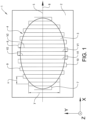
- Figure 1 is a schematic view of a build layer 1 in an additive manufacturing (AM) machine.
- the build layer 1 is seen in the vertical direction in parallel with the Z-axis perpendicular to the XY-plane, whereas the main extension of the build layer 1 is in the XY-plane.
- the build layer 1 has a first section 2 of non-melted powder and a second section 3 of solid material formed by previously melted powder, i.e. the area inside the oval.
- the solid material constitutes one layer of a three-dimensional article being manufactured layer by layer in the AM machine.
- the AM machine is schematically illustrated in Figures 3 and 4 .
- the build layer 1 may include non-melted powder, bonded powder and previously melted powder that has solidified.
- the method described hereinafter is performed in an AM machine.
- the method is implemented when forming such a three-dimensional article layer by layer by successive fusion of selected areas of powder layers, which selected areas correspond to successive layers of the three-dimensional article.
- the equipment for melting the powder can be any suitable device for transferring energy to the selected areas, such as an electron beam source or laser source.
- the method for analyzing the build layer is performed before, after or in between such melting operations.
- the method for analyzing the build layer 1, preferably the surface of the build layer comprises the steps of radiating a portion 4 of the build layer 1 by an energy beam and detecting particles emitted, backscattered or reflected from the radiated portion of the build layer, and scanning the portion of the build layer by moving the energy beam along a main path 5 and simultaneously moving the energy beam back-and-forth across the main path in a meandering pattern 6.
- the radiation of the build layer is performed during scanning the portion 4 of the build layer and the portion 4 is determined by the scanning path.
- a portion of the top surface of the build layer is scanned.
- the method is primarily directed to the analysis of the properties of the surface and the material of the surface or immediately under the surface.
- Such a meandering pattern 6 is illustrated in Figure 1 .
- the meandering pattern 6 shows the path 7 of the energy beam when the second section 3 of solid material is scanned for analysing the surface.
- the main path 5 has a direction 8 from left to the right in parallel with the X-axis.
- the energy beam path 7 is repeatedly crossing the main path 5 and has a direction component alternating between being directed downwards in parallel with the Y-axis and upwards in parallel with the Y-axis.
- the energy beam is moved in a continuous meandering pattern 6.
- the energy beam is moved in the meandering pattern 6 having alternating peaks 9 and valleys 10.
- a square wave shaped meandering pattern is illustrated and described hereinafter, also other meandering patterns could be used, such as a sinusoidal, triangle or sick-sack shaped pattern.
- a distance in a direction orthogonal to the direction of the main path between a peak and a subsequent valley of the meandering pattern is indicated by "y”
- a distance in parallel with the direction of the main path between two consecutive peaks of the meandering pattern is indicated by "x”.
- the distance y is dependent on the size and shape of the surface portion to be analysed, but is in the range 1 mm ⁇ y ⁇ 100 mm, more preferably 2 mm ⁇ y ⁇ 50 mm, and often in the range 4 mm ⁇ y ⁇ 10 mm.
- the distance x is dependent on the detection resolution required and is in the range 2 ⁇ m ⁇ x ⁇ 1000 ⁇ m, more preferably in the range 5 ⁇ m ⁇ x ⁇ 500 ⁇ m, and often in the range 10 ⁇ m ⁇ x ⁇ 100 ⁇ m.
- the method comprises the step of moving the energy beam in alternating directions in parallel vectors V1, V2 crossing the main path 5, and moving the energy beam in the parallel vectors V1, V2 being orthogonal to the direction 8 of the main path 5.
- parallel and orthogonal are meant to comprise also such patterns where the vectors V1, V2 are substantially parallel to each other and substantially orthogonal to the main path, including small angle deviations in the size of 0-20°, preferably 0-10°, and more preferably 0-5°, from the current directions.
- the meandering pattern 6 has a plurality of first scan vectors V 1 directed downwardly in parallel with the Y-axis and a plurality of second scan vectors V2 directed upwardly in parallel with the Y-axis in Figure 1 .
- each first vector V1 is followed by one second vector V2 that is followed by one first vector V1, etc.
- Each vector V1, V2 can be connected to the adjacent vectors. In other words; between two adjacent vectors the energy beam is moved in the main path direction 8.
- the energy beam is moved downwards in parallel with the Y-axis forming a vector V1, then from left to right along the main path direction 8, thereafter upwards in parallel with the Y-axis forming a vector V2, and again from left to right along the main path direction 8.
- This sequence is then repeated until the surface portion is properly scanned.
- the length of the first and second vectors V1, V2 may vary among themselves along the main path 5 depending on the shape of the surface portion to be analysed.
- the distance between two adjacent vectors is selected based on the resolution requirement as previously described, and preferably the distance between two adjacent vectors V1, V2 is in the range 1-500 ⁇ m.
- Figure 2 shows another meandering pattern 16 associated to a further example embodiment where the method comprises the step of moving the energy beam along the main path 15 being selected on the basis of a boundary 20 between a previously melted and solidified section 13 and a non-melted section 12 of the build layer 11.
- the energy beam is preferably moved such that the main path 15 substantially follows the boundary 20, although the main path can be selected on the basis of the boundary, but the energy beam is moved somewhat differently.
- the main path can be off-set relative to the boundary but still follow the contour of the boundary. Then the non-melted powder on one side of the boundary and/or the solid material on the other side of the boundary can be scanned.
- the main path can oscillate about the boundary.
- the main path 15 can preferably follow the boundary 20.
- the main path direction 18 is not constant but varies along the boundary 20 in accordance with the direction changes of the boundary.
- the meandering pattern has first vectors V1 and second vectors V2. These vectors V1, V2 are preferably parallel to each other.
- the vectors can be substantially orthogonal to the main path, they don't need to always be orthogonal to the main path 15.
- the vectors have instead a direction along a first axis or a second axis, where the first axis and the second axis are substantially perpendicular to each other.
- these two axes can be the Y-axis and the X-axis.
- the vectors extend in a direction in parallel with the Y-axis and in the right portion of the boundary 20, the vectors extend in a direction in parallel with the X-axis.
- the vectors can be adapted to the size of the surface portion to be analysed.
- the length of each vector and the position of each vector relative to the boundary 20, can be selected for scanning the desired area.
- Each vector can be divided into a vector part extending from the boundary 20 to a position on the solid layer inside of the boundary 20 and a vector part extending from the boundary 20 to a position on the non-melted powder outside of the boundary 20.
- the vectors can extend between an inner imagined line 21 and an outer imagined line 22, where the distance S between the inner line 21 and the boundary is in the range 1-5 mm for instance, and the distance P between the boundary 20 and the outer line 22 is in the range 1-5 mm for instance.
- the imagined inner and outer lines 21, 22 may have substantially the same shape as the boundary 20.
- the example embodiments described herein may comprise the step of moving the energy beam along the main path 5, 15 being selected on the basis of a path along which an electron beam or laser beam has been previously moved for melting the powder layer.
- the energy beam can be moved along the main path 5, 15 which substantially follows a path along which an electron beam or a laser beam has been previously moved for melting the powder bed. This will simplify the control of the energy beam, particularly if the same energy beam source is used for both melting and/or pre-heating powder and for subsequently radiating the build layer surface for analyzing purposes.
- an arrangement 50 for an AM machine is schematically illustrated.
- the arrangement comprises a control unit 32 and a particle detector device 31.
- an electron beam source 30 is schematically illustrated.
- the control unit 32 is arranged for controlling an electron beam 33 for analysing a surface of a build layer 34 by radiating a portion of the surface of the build layer by the electron beam and detecting electrons emitted or back-scattered from the radiated portion of the build layer by the particle detector device 31.
- the control unit 32 is configured to control the electron beam 33 to move along a main path and simultaneously back-and-forth across the main path in a meandering pattern as previously described hereinabove.
- the electron beam source 30 can be designed in a way well known to the person skilled in the art.
- the electron beam source may have an electron gun 35 with an emitter electrode which is connected to a high voltage circuit and a current source for accelerating electrons and releasing electrons from the emitter electrode. These electrons form the electron beam 33.
- the electron beam source 30 has also focusing coils and deflection coils 36 for directing the electron beam to various positions of the build layer surface.
- the electron beam source 30 has further deflection amplifiers 37 connected to the deflection coils 36.
- the portion of the build layer to be analysed is radiated by an electron beam that can have a beam current IB in the range 1 ⁇ A ⁇ IB ⁇ 1000 ⁇ A, preferably in the range 5 ⁇ A ⁇ IB ⁇ 500 ⁇ A, and often in the range 10 ⁇ A ⁇ IB ⁇ 100 ⁇ A.
- the beam power PB can be in the range 5 mW ⁇ PB ⁇ 50000 mW, preferably in the range 500 mW ⁇ PB ⁇ 5000 mW.
- the deflecting coils 36 and the deflection amplifiers 37 are schematically illustrated in Figure 3 .
- the control unit 32 controls the electron beam 33 by transmitting signals to the deflection coils 36 via the deflection amplifiers 37.
- the point or spot of the electron beam 33 positioned on the build layer surface can be moved in the meandering pattern.
- the detected particles can be for example back-scattered electrons originating from the electron beam source 30 or secondary electrons emitted from the material of the build layer surface.
- the particle detector device 31 may use any suitable equipment for detecting electrons.
- the particle detector device can have an additional bias voltage for selective detection of the electrons.
- the particle detector device 31 can generate data signals to be transmitted to the control unit 32. The data can be further processed and utilized for different analysis, for example creating images of the build layer surface for identifying defects or anomalies.
- the particle detector device preferably is an electron detector device 31, it would also be possible to use a photon detector device, since photons can be emitted from the build layer surface as a physical reaction to the target materials intrinsic interaction with the absorbed energy from the electron beam 33.
- a photon detector device may use any suitable equipment, such as for example photodiode, phototransistor, CCD, CMOS, PMT or similar.
- the control unit 32 may comprise one or more microprocessors and/or one or more memory devices or any other components for executing computer programs to perform the method. Thus, the control unit 32 is preferably provided with a computer program for performing all steps of any embodiment of the method described hereinabove.
- the control unit can be a separate component or be integrated in another controller.
- the control unit can be arranged to control other parameters of the energy beam source, such as the energy beam current or the energy beam power.
- the control unit 32 can be part of a controller used also for other functions of the AM machine, such as movement of the build plate, control of a powder distribution device, etc.
- the arrangement 50 for an AM machine and the control unit 32 itself can be combined with any of the features disclosed hereinabove, for example discussed with reference to the method and/or related to the AM machine.
- a program element configured and arranged when executed on a computer (e.g., via a computer program) to implement the method described herein.
- the program element may be installed in a non-transitory computer readable storage medium.
- the computer readable storage medium may be the control unit 32 or on another control unit.
- the computer readable storage medium and the program element, which may comprise computer-readable program code portions embodied therein, may further be contained within a computer program product or a computer program, as described previously.
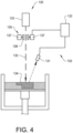
- FIG 4 a further example embodiment of an arrangement 150 for an AM machine is schematically illustrated.
- the arrangement 150 comprises a control unit 132 and a particle detector device in form of a photon detector device 131.
- a laser beam source 130 is schematically illustrated.
- the control unit 132 is arranged for controlling a laser beam 133 for analysing a surface of a build layer 134 by radiating a portion of the surface of the build layer by the laser beam and detecting photons emitted or reflected from the radiated portion of the build layer by the photon detector device 131.
- the control unit 132 is configured to control the laser beam 133 to move along a main path and simultaneously back-and-forth across the main path in a meandering pattern as previously described hereinabove.
- the laser beam source 130 can be designed in a way well known to the person skilled in the art.
- the laser beam source may have a laser emitter 135 for emitting photons. These photons form the laser beam 133.
- the laser beam source 130 has also focusing units and deflection units 136 for directing the laser beam to various positions of the build layer surface.
- the focusing units can comprise lenses.
- Each deflection unit 136 may comprise a deflection actuator 138 and a deflection driver 137 for controlling the movement of the deflection actuator 138.
- the deflection actuators 138 are suitably mirrors.
- the deflecting actuators 138 and the deflection drivers 137 are schematically illustrated in Figure 4 .
- the control unit 132 controls the laser beam 133 by transmitting signals to the deflection drivers 137.
- the point or spot of the laser beam 133 positioned on the build layer surface can be moved in the meandering pattern.
- the laser beam 133 will transfer significantly less energy to the surface than the energy required for melting the powder.
- the laser beam power PB can be in the range 100 mW ⁇ PB ⁇ 1000 mW.
- the detected photons can be reflected or backscattered photons originating from the laser beam.
- the photon detector device 131 may use any suitable equipment, such as for example photodiode, phototransistor, CCD, CMOS, PMT or similar.
- the photon detector device 131 can generate data signals to be transmitted to the control unit 132.
- the data can be further processed and utilized for different analysis, for example creating images of the build layer surface for identifying defects or anomalies.
- a program element configured and arranged when executed on a computer to implement a method as described herein.
- the program element may be installed in a computer readable storage medium.
- the computer readable storage medium may be any one of the control units described elsewhere herein or another and separate control unit, as may be desirable.
- the computer readable storage medium and the program element, which may comprise computer-readable program code portions embodied therein, may further be contained within a non-transitory computer program product. Further details regarding these features and configurations are provided, in turn, below.
- a computer program product may include a non-transitory computer-readable storage medium storing applications, programs, program modules, scripts, source code, program code, object code, byte code, compiled code, interpreted code, machine code, executable instructions, and/or the like (also referred to herein as executable instructions, instructions for execution, program code, and/or similar terms used herein interchangeably).
- Such non-transitory computer-readable storage media include all computer-readable media (including volatile and non-volatile media).
- a non-volatile computer-readable storage medium may include a floppy disk, flexible disk, hard disk, solid-state storage (SSS) (e.g., a solid state drive (SSD), solid state card (SSC), solid state module (SSM)), enterprise flash drive, magnetic tape, or any other non-transitory magnetic medium, and/or the like.
- SSD solid state drive
- SSC solid state card
- SSM solid state module
- a non-volatile computer-readable storage medium may also include a punch card, paper tape, optical mark sheet (or any other physical medium with patterns of holes or other optically recognizable indicia), compact disc read only memory (CD-ROM), compact disc compact disc-rewritable (CD-RW), digital versatile disc (DVD), Blu-ray disc (BD), any other non-transitory optical medium, and/or the like.
- CD-ROM compact disc read only memory
- CD-RW compact disc compact disc-rewritable
- DVD digital versatile disc
- BD Blu-ray disc
- Such a non-volatile computer-readable storage medium may also include read-only memory (ROM), programmable read-only memory (PROM), erasable programmable read-only memory (EPROM), electrically erasable programmable read-only memory (EEPROM), flash memory (e.g., Serial, NAND, NOR, and/or the like), multimedia memory cards (MMC), secure digital (SD) memory cards, SmartMedia cards, CompactFlash (CF) cards, Memory Sticks, and/or the like.
- ROM read-only memory
- PROM programmable read-only memory
- EPROM erasable programmable read-only memory
- EEPROM electrically erasable programmable read-only memory
- flash memory e.g., Serial, NAND, NOR, and/or the like
- MMC multimedia memory cards
- SD secure digital
- SmartMedia cards SmartMedia cards
- CompactFlash (CF) cards Memory Sticks, and/or the like.
- a non-volatile computer-readable storage medium may also include conductive-bridging random access memory (CBRAM), phase-change random access memory (PRAM), ferroelectric random-access memory (FeRAM), non-volatile random-access memory (NVRAM), magnetoresistive random-access memory (MRAM), resistive random-access memory (RRAM), Silicon-Oxide-Nitride-Oxide-Silicon memory (SONOS), floating junction gate random access memory (FJG RAM), Millipede memory, racetrack memory, and/or the like.
- CBRAM conductive-bridging random access memory
- PRAM phase-change random access memory
- FeRAM ferroelectric random-access memory
- NVRAM non-volatile random-access memory
- MRAM magnetoresistive random-access memory
- RRAM resistive random-access memory
- SONOS Silicon-Oxide-Nitride-Oxide-Silicon memory
- FJG RAM floating junction gate random access memory
- Millipede memory racetrack memory
- a volatile computer-readable storage medium may include random access memory (RAM), dynamic random access memory (DRAM), static random access memory (SRAM), fast page mode dynamic random access memory (FPM DRAM), extended data-out dynamic random access memory (EDO DRAM), synchronous dynamic random access memory (SDRAM), double data rate synchronous dynamic random access memory (DDR SDRAM), double data rate type two synchronous dynamic random access memory (DDR2 SDRAM), double data rate type three synchronous dynamic random access memory (DDR3 SDRAM), Rambus dynamic random access memory (RDRAM), Twin Transistor RAM (TTRAM), Thyristor RAM (T-RAM), Zero-capacitor (Z-RAM), Rambus in-line memory module (RIMM), dual in-line memory module (DIMM), single in-line memory module (SIMM), video random access memory VRAM, cache memory (including various levels), flash memory, register memory, and/or the like.
- RAM random access memory
- DRAM dynamic random access memory
- SRAM static random access memory
- FPM DRAM fast page mode dynamic random access memory
- embodiments of the present invention may also be implemented as methods, apparatus, systems, computing devices, computing entities, and/or the like, as have been described elsewhere herein.
- embodiments of the present invention may take the form of an apparatus, system, computing device, computing entity, and/or the like executing instructions stored on a computer-readable storage medium to perform certain steps or operations.
- embodiments of the present invention may also take the form of an entirely hardware embodiment performing certain steps or operations.
- These computer program instructions may also be stored in a computer-readable memory that can direct a computer or other programmable data processing apparatus to function in a particular manner, such that the instructions stored in the computer-readable memory produce an article of manufacture including computer-readable instructions for implementing the functionality specified in the flowchart block or blocks.
- the computer program instructions may also be loaded onto a computer or other programmable data processing apparatus to cause a series of operational steps to be performed on the computer or other programmable apparatus to produce a computer-implemented process such that the instructions that execute on the computer or other programmable apparatus provide operations for implementing the functions specified in the flowchart block or blocks.
- blocks of the block diagrams and flowchart illustrations support various combinations for performing the specified functions, combinations of operations for performing the specified functions and program instructions for performing the specified functions. It should also be understood that each block of the block diagrams and flowchart illustrations, and combinations of blocks in the block diagrams and flowchart illustrations, could be implemented by special purpose hardware-based computer systems that perform the specified functions or operations, or combinations of special purpose hardware and computer instructions.
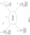
- Figure 5 is a block diagram of an exemplary system 320 that can be used in conjunction with various embodiments of the present invention.
- the system 320 may include one or more central computing devices 110, one or more distributed computing devices 120, and one or more distributed handheld or mobile devices 300, all configured in communication with a central server 200 (or control unit) via one or more networks 130.
- Figure 5 illustrates the various system entities as separate, standalone entities, the various embodiments are not limited to this particular architecture.
- the one or more networks 130 may be capable of supporting communication in accordance with any one or more of a number of second-generation (2G), 2.5G, third-generation (3 G), and/or fourth-generation (4G) mobile communication protocols, or the like. More particularly, the one or more networks 130 may be capable of supporting communication in accordance with 2G wireless communication protocols IS-136 (TDMA), GSM, and IS-95 (CDMA). Also, for example, the one or more networks 130 may be capable of supporting communication in accordance with 2.5G wireless communication protocols GPRS, Enhanced Data GSM Environment (EDGE), or the like.
- 2G wireless communication protocols IS-136 (TDMA), GSM, and IS-95 (CDMA) IS-136
- CDMA IS-95
- the one or more networks 130 may be capable of supporting communication in accordance with 2.5G wireless communication protocols GPRS, Enhanced Data GSM Environment (EDGE), or the like.
- the one or more networks 130 may be capable of supporting communication in accordance with 3G wireless communication protocols such as Universal Mobile Telephone System (UMTS) network employing Wideband Code Division Multiple Access (WCDMA) radio access technology.
- UMTS Universal Mobile Telephone System
- WCDMA Wideband Code Division Multiple Access
- Some narrow-band AMPS (NAMPS), as well as TACS, network(s) may also benefit from embodiments of the present invention, as should dual or higher mode mobile stations (e.g., digital/analog or TDMA/CDMA/analog phones).
- each of the components of the system 320 may be configured to communicate with one another in accordance with techniques such as, for example, radio frequency (RF), Bluetooth TM , infrared (IrDA), or any of a number of different wired or wireless networking techniques, including a wired or wireless Personal Area Network (“PAN”), Local Area Network (“LAN”), Metropolitan Area Network (“MAN”), Wide Area Network (“WAN”), or the like.
- RF radio frequency
- IrDA infrared
- PAN Personal Area Network
- LAN Local Area Network
- MAN Metropolitan Area Network
- WAN Wide Area Network
- the device(s) 110-300 are illustrated in Figure 5 as communicating with one another over the same network 130, these devices may likewise communicate over multiple, separate networks.
- the distributed devices 110, 120, and/or 300 may be further configured to collect and transmit data on their own.
- the devices 110, 120, and/or 300 may be capable of receiving data via one or more input units or devices, such as a keypad, touchpad, barcode scanner, radio frequency identification (RFID) reader, interface card (e.g., modem, etc.) or receiver.
- the devices 110, 120, and/or 300 may further be capable of storing data to one or more volatile or non-volatile memory modules, and outputting the data via one or more output units or devices, for example, by displaying data to the user operating the device, or by transmitting data, for example over the one or more networks 130.
- the server 200 includes various systems for performing one or more functions in accordance with various embodiments of the present invention, including those more particularly shown and described herein. It should be understood, however, that the server 200 might include a variety of alternative devices for performing one or more like functions, without departing from the spirit and scope of the present invention. For example, at least a portion of the server 200, in certain embodiments, may be located on the distributed device(s) 110, 120, and/or the handheld or mobile device(s) 300, as may be desirable for particular applications.
- the handheld or mobile device(s) 300 may contain one or more mobile applications 330 which may be configured so as to provide a user interface for communication with the server 200, all as will be likewise described in further detail below.
- FIG. 6 is a schematic diagram of the server 200 according to various embodiments.
- the server 200 includes a processor 230 that communicates with other elements within the server via a system interface or bus 235. Also included in the server 200 is a display/input device 250 for receiving and displaying data. This display/input device 250 may be, for example, a keyboard or pointing device that is used in combination with a monitor.
- the server 200 further includes memory 220, which typically includes both read only memory (ROM) 226 and random access memory (RAM) 222.
- the server's ROM 226 is used to store a basic input/output system 224 (BIOS), containing the basic routines that help to transfer information between elements within the server 200.
- BIOS basic input/output system
- the server 200 includes at least one storage device or program storage 210, such as a hard disk drive, a floppy disk drive, a CD Rom drive, or optical disk drive, for storing information on various computer-readable media, such as a hard disk, a removable magnetic disk, or a CD-ROM disk.
- storage devices 210 are connected to the system bus 235 by an appropriate interface.
- the storage devices 210 and their associated computer-readable media provide nonvolatile storage for a personal computer.
- the computer-readable media described above could be replaced by any other type of computer-readable media known in the art. Such media include, for example, magnetic cassettes, flash memory cards, digital video disks, and Bernoulli cartridges.
- the storage device 210 and/or memory of the server 200 may further provide the functions of a data storage device, which may store historical and/or current delivery data and delivery conditions that may be accessed by the server 200.
- the storage device 210 may comprise one or more databases.
- database refers to a structured collection of records or data that is stored in a computer system, such as via a relational database, hierarchical database, or network database and as such, should not be construed in a limiting fashion.
- a number of program modules (e.g., exemplary modules 400-700) comprising, for example, one or more computer-readable program code portions executable by the processor 230, may be stored by the various storage devices 210 and within RAM 222. Such program modules may also include an operating system 280. In these and other embodiments, the various modules 400, 500, 600, 700 control certain aspects of the operation of the server 200 with the assistance of the processor 230 and operating system 280. In still other embodiments, it should be understood that one or more additional and/or alternative modules may also be provided, without departing from the scope and nature of the present invention.
- the program modules 400, 500, 600, 700 are executed by the server 200 and are configured to generate one or more graphical user interfaces, reports, instructions, and/or notifications/alerts, all accessible and/or transmittable to various users of the system 320.
- the user interfaces, reports, instructions, and/or notifications/alerts may be accessible via one or more networks 130, which may include the Internet or other feasible communications network, as previously discussed.
- one or more of the modules 400, 500, 600, 700 may be alternatively and/or additionally (e.g., in duplicate) stored locally on one or more of the devices 110, 120, and/or 300 and may be executed by one or more processors of the same.
- the modules 400, 500, 600, 700 may send data to, receive data from, and utilize data contained in one or more databases, which may be comprised of one or more separate, linked and/or networked databases.
- a network interface 260 for interfacing and communicating with other elements of the one or more networks 130. It will be appreciated by one of ordinary skill in the art that one or more of the server 200 components may be located geographically remotely from other server components. Furthermore, one or more of the server 200 components may be combined, and/or additional components performing functions described herein may also be included in the server.
- the server 200 may comprise multiple processors operating in conjunction with one another to perform the functionality described herein.
- the processor 230 can also be connected to at least one interface or other means for displaying, transmitting and/or receiving data, content or the like.
- the interface(s) can include at least one communication interface or other means for transmitting and/or receiving data, content or the like, as well as at least one user interface that can include a display and/or a user input interface, as will be described in further detail below.
- the user input interface in turn, can comprise any of a number of devices allowing the entity to receive data from a user, such as a keypad, a touch display, a joystick or other input device.
- embodiments of the present invention are not limited to traditionally defined server architectures. Still further, the system of embodiments of the present invention is not limited to a single server, or similar network entity or mainframe computer system. Other similar architectures including one or more network entities operating in conjunction with one another to provide the functionality described herein may likewise be used without departing from the spirit and scope of embodiments of the present invention. For example, a mesh network of two or more personal computers (PCs), similar electronic devices, or handheld portable devices, collaborating with one another to provide the functionality described herein in association with the server 200 may likewise be used without departing from the spirit and scope of embodiments of the present invention.
- PCs personal computers
- similar electronic devices or handheld portable devices
- many individual steps of a process may or may not be carried out utilizing the computer systems and/or servers described herein, and the degree of computer implementation may vary, as may be desirable and/or beneficial for one or more particular applications.
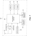
- FIG. 7 provides an illustrative schematic representative of a mobile device 300 that can be used in conjunction with various embodiments of the present invention.
- Mobile devices 300 can be operated by various parties.
- a mobile device 300 may include an antenna 312, a transmitter 304 (e.g., radio), a receiver 306 (e.g., radio), and a processing element 308 that provides signals to and receives signals from the transmitter 304 and receiver 306, respectively.
- a transmitter 304 e.g., radio
- a receiver 306 e.g., radio
- a processing element 308 that provides signals to and receives signals from the transmitter 304 and receiver 306, respectively.
- the signals provided to and received from the transmitter 304 and the receiver 306, respectively, may include signaling data in accordance with an air interface standard of applicable wireless systems to communicate with various entities, such as the server 200, the distributed devices 110, 120, and/or the like.
- the mobile device 300 may be capable of operating with one or more air interface standards, communication protocols, modulation types, and access types. More particularly, the mobile device 300 may operate in accordance with any of a number of wireless communication standards and protocols.
- the mobile device 300 may operate in accordance with multiple wireless communication standards and protocols, such as GPRS, UMTS, CDMA2000, 1xRTT, WCDMA, TD-SCDMA, LTE, E-UTRAN, EVDO, HSPA, HSDPA, Wi-Fi, WiMAX, UWB, IR protocols, Bluetooth protocols, USB protocols, and/or any other wireless protocol.
- multiple wireless communication standards and protocols such as GPRS, UMTS, CDMA2000, 1xRTT, WCDMA, TD-SCDMA, LTE, E-UTRAN, EVDO, HSPA, HSDPA, Wi-Fi, WiMAX, UWB, IR protocols, Bluetooth protocols, USB protocols, and/or any other wireless protocol.
- the mobile device 300 may according to various embodiments communicate with various other entities using concepts such as Unstructured Supplementary Service data (USSD), Short Message Service (SMS), Multimedia Messaging Service (MMS), Dual-Tone Multi-Frequency Signaling (DTMF), and/or Subscriber Identity Module Dialer (SIM dialer).
- USSD Unstructured Supplementary Service data
- SMS Short Message Service
- MMS Multimedia Messaging Service
- DTMF Dual-Tone Multi-Frequency Signaling
- SIM dialer Subscriber Identity Module Dialer
- the mobile device 300 can also download changes, add-ons, and updates, for instance, to its firmware, software (e.g., including executable instructions, applications, program modules), and operating system.
- the mobile device 300 may include a location determining device and/or functionality.
- the mobile device 300 may include a GPS module adapted to acquire, for example, latitude, longitude, altitude, geocode, course, and/or speed data.
- the GPS module acquires data, sometimes known as ephemeris data, by identifying the number of satellites in view and the relative positions of those satellites.
- the mobile device 300 may also comprise a user interface (that can include a display 316 coupled to a processing element 308) and/or a user input interface (coupled to a processing element 308).
- the user input interface can comprise any of a number of devices allowing the mobile device 300 to receive data, such as a keypad 318 (hard or soft), a touch display, voice or motion interfaces, or other input device.
- the keypad can include (or cause display of) the conventional numeric (0-9) and related keys (#, *), and other keys used for operating the mobile device 300 and may include a full set of alphabetic keys or set of keys that may be activated to provide a full set of alphanumeric keys.
- the user input interface can be used, for example, to activate or deactivate certain functions, such as screen savers and/or sleep modes.
- the mobile device 300 can also include volatile storage or memory 322 and/or non-volatile storage or memory 324, which can be embedded and/or may be removable.
- the non-volatile memory may be ROM, PROM, EPROM, EEPROM, flash memory, MMCs, SD memory cards, Memory Sticks, CBRAM, PRAM, FeRAM, RRAM, SONOS, racetrack memory, and/or the like.
- the volatile memory may be RAM, DRAM, SRAM, FPM DRAM, EDO DRAM, SDRAM, DDR SDRAM, DDR2 SDRAM, DDR3 SDRAM, RDRAM, RIMM, DIMM, SIMM, VRAM, cache memory, register memory, and/or the like.
- the volatile and non-volatile storage or memory can store databases, database instances, database mapping systems, data, applications, programs, program modules, scripts, source code, object code, byte code, compiled code, interpreted code, machine code, executable instructions, and/or the like to implement the functions of the mobile device 300.
- the mobile device 300 may also include one or more of a camera 326 and a mobile application 330.
- the camera 326 may be configured according to various embodiments as an additional and/or alternative data collection feature, whereby one or more items may be read, stored, and/or transmitted by the mobile device 300 via the camera.
- the mobile application 330 may further provide a feature via which various tasks may be performed with the mobile device 300.
- Various configurations may be provided, as may be desirable for one or more users of the mobile device 300 and the system 320 as a whole.
Landscapes
- Engineering & Computer Science (AREA)
- Chemical & Material Sciences (AREA)
- Materials Engineering (AREA)
- Manufacturing & Machinery (AREA)
- Physics & Mathematics (AREA)
- Optics & Photonics (AREA)
- Automation & Control Theory (AREA)
- Mechanical Engineering (AREA)
- Theoretical Computer Science (AREA)
- Plasma & Fusion (AREA)
- Analytical Chemistry (AREA)
- Computer Hardware Design (AREA)
- Evolutionary Computation (AREA)
- Geometry (AREA)
- General Engineering & Computer Science (AREA)
- General Physics & Mathematics (AREA)
- Powder Metallurgy (AREA)
- Architecture (AREA)
- Software Systems (AREA)
- Welding Or Cutting Using Electron Beams (AREA)
Claims (13)
- Une méthode d'analyse d'une couche de construction (1; 11) dans une machine de fabrication additive lors de la formation d'un article tridimensionnel couche par couche par fusion successive de zones sélectionnées de couches de poudre, les zones sélectionnées correspondant à des couches successives de l'article tridimensionnel, la méthode comprenant les étapes de:rayonnant, avant, après ou entre les opérations de fusion, une portion (4; 14) de la couche de construction (1; 11) par un faisceau d'énergie,détecter les particules émises, rétrodiffusées ou réfléchies par la partie rayonnée de la couche de construction, caractérisées par:
balayage de la portion (4; 14) de la couche de construction en déplaçant le faisceau d'énergie le long d'un chemin principal (5; 15) et en déplaçant simultanément le faisceau d'énergie aller-retour sur le chemin principal selon un schéma sinueux (6; 16) ayant des pics alternés (9) et des vallées (10), de telle sorte qu'une distance dans une direction orthogonale à la direction (8) du sentier principal (5) entre un pic et une vallée subséquente du motif sinueux est y, où 1<y<100 mm, et une distance parallèle à la direction du sentier principal entre deux pics consécutifs du motif sinueux est x, où 2<x<1000 µm, où le déplacement du faisceau d'énergie se produit dans un motif sinueux continu (6; 16). - La méthode selon la revendication 1, dans laquelle le déplacement du faisceau d'énergie le long du chemin principal (15) est sélectionné sur la base d'une limite (20) entre une section préalablement fondue et une section non fondue de la couche de construction (11).
- La méthode selon la revendication 1, dans laquelle le déplacement du faisceau d'énergie le long du chemin principal (15) se produit essentiellement après une limite (20) entre une section préalablement fondue et une section non fondue de la couche de construction (11).
- La méthode selon l'une quelconque des revendications 1-3, dans laquelle le déplacement du faisceau d'énergie le long du chemin principal (5; 15) est sélectionné sur la base d'un chemin le long duquel un faisceau d'électrons ou un faisceau laser a déjà été déplacé pour faire fondre la couche de construction (1; 11).
- La méthode selon l'une quelconque des revendications 1-4, dans laquelle le déplacement du faisceau d'énergie le long du chemin principal (5; 15) se produit essentiellement en suivant un chemin le long duquel un faisceau d'électrons ou un faisceau laser a déjà été déplacé pour faire fondre la couche de construction (1; 11).
- La méthode selon l'une quelconque des revendications 1 à 5, dans laquelle le déplacement du faisceau d'énergie se produit de telle sorte qu'une section non fondue (12) de la couche de construction est rayonnée pour détecter les particules émises, rétrodiffusées ou réfléchies à partir de la section non fondue.
- La méthode selon l'une quelconque des revendications 1 à 6, dans laquelle le déplacement du faisceau d'énergie se produit de telle sorte qu'une section préalablement fondue et solidifiée (3; 13) de la couche de construction est rayonnée pour détecter les particules émises, rétrodiffusées ou réfléchies par la section préalablement fondue et solidifiée.
- La méthode selon la revendication 1, dans laquelle y est 2<y<50 mm et x est 5<x<500 µm.
- La méthode selon l'une quelconque des revendications 1 à 8, dans laquelle le déplacement du faisceau d'énergie se produit dans des directions alternées dans des vecteurs parallèles (V1, V2) traversant le chemin principal (5; 15).
- La méthode selon la revendication 9, dans laquelle le déplacement du faisceau d'énergie dans les vecteurs parallèles (V1, V2) est orthogonal à la direction du chemin principal (5).
- La méthode selon la revendication 9, dans laquelle le déplacement du faisceau d'énergie dans le modèle sinueux (6; 16) est essentiellement en forme d'onde carrée.
- La méthode selon l'une quelconque des revendications 1 à 11, dans laquelle le faisceau d'énergie est un faisceau d'électrons (33).
- La méthode selon la revendication 12, comprenant en outre l'étape consistant à rayonner la portion (4; 14) de la couche de construction par le faisceau d'électrons (33), dans lequel le faisceau d'électrons (33) a un courant de faisceau IB dans la gamme 1<IB<1000 µA.
Applications Claiming Priority (3)
| Application Number | Priority Date | Filing Date | Title |
|---|---|---|---|
| US201762590909P | 2017-11-27 | 2017-11-27 | |
| US16/154,444 US10821721B2 (en) | 2017-11-27 | 2018-10-08 | Method for analysing a build layer |
| PCT/EP2018/082590 WO2019102006A1 (fr) | 2017-11-27 | 2018-11-26 | Procédé d'analyse d'une couche de construction dans la fabrication additive |
Publications (2)
| Publication Number | Publication Date |
|---|---|
| EP3717153A1 EP3717153A1 (fr) | 2020-10-07 |
| EP3717153B1 true EP3717153B1 (fr) | 2024-09-18 |
Family
ID=64556887
Family Applications (1)
| Application Number | Title | Priority Date | Filing Date |
|---|---|---|---|
| EP18811210.6A Active EP3717153B1 (fr) | 2017-11-27 | 2018-11-26 | Procédé d'analyse d'une couche de construction dans la fabrication additive |
Country Status (5)
| Country | Link |
|---|---|
| US (1) | US10821721B2 (fr) |
| EP (1) | EP3717153B1 (fr) |
| JP (1) | JP7020745B2 (fr) |
| CN (1) | CN111405954B (fr) |
| WO (1) | WO2019102006A1 (fr) |
Families Citing this family (4)
| Publication number | Priority date | Publication date | Assignee | Title |
|---|---|---|---|---|
| DE102018202600A1 (de) * | 2018-02-21 | 2019-08-22 | Siemens Aktiengesellschaft | SLM-Anlage und Verfahren zum Betreiben der SLM-Anlage |
| JP7008669B2 (ja) * | 2019-09-09 | 2022-01-25 | 日本電子株式会社 | 3次元積層造形装置及び3次元積層造形方法 |
| JP6954963B2 (ja) * | 2019-09-09 | 2021-10-27 | 日本電子株式会社 | 3次元積層造形方法及び3次元積層造形装置 |
| US20240017492A1 (en) * | 2020-11-30 | 2024-01-18 | Ihi Corporation | Three-dimensional modeling device and three-dimensional modeling method |
Citations (1)
| Publication number | Priority date | Publication date | Assignee | Title |
|---|---|---|---|---|
| US6570155B1 (en) * | 2000-04-11 | 2003-05-27 | Applied Materials, Inc. | Bi-directional electron beam scanning apparatus |
Family Cites Families (242)
| Publication number | Priority date | Publication date | Assignee | Title |
|---|---|---|---|---|
| US2264968A (en) | 1938-02-14 | 1941-12-02 | Magnafiux Corp | Apparatus for measuring wall thickness |
| US2323715A (en) | 1941-10-17 | 1943-07-06 | Gen Electric | Thermal testing apparatus |
| US3634644A (en) | 1968-12-30 | 1972-01-11 | Ogden Eng Corp | Method and apparatus for welding together beam components |
| US3882477A (en) | 1973-03-26 | 1975-05-06 | Peter H Mueller | Smoke and heat detector incorporating an improved smoke chamber |
| US3838496A (en) | 1973-04-09 | 1974-10-01 | C Kelly | Welding apparatus and method |
| US3906229A (en) | 1973-06-12 | 1975-09-16 | Raytheon Co | High energy spatially coded image detecting systems |
| US3908124A (en) | 1974-07-01 | 1975-09-23 | Us Energy | Phase contrast in high resolution electron microscopy |
| US4348576A (en) | 1979-01-12 | 1982-09-07 | Steigerwald Strahltechnik Gmbh | Position regulation of a charge carrier beam |
| US4314134A (en) | 1979-11-23 | 1982-02-02 | Ford Motor Company | Beam position control for electron beam welder |
| JPS56156767A (en) | 1980-05-02 | 1981-12-03 | Sumitomo Electric Ind Ltd | Highly hard substance covering material |
| US4352565A (en) | 1981-01-12 | 1982-10-05 | Rowe James M | Speckle pattern interferometer |
| US4541055A (en) | 1982-09-01 | 1985-09-10 | Westinghouse Electric Corp. | Laser machining system |
| JPS60181638A (ja) | 1984-02-29 | 1985-09-17 | Toshiba Corp | 放射線像撮影装置 |
| US4863538A (en) | 1986-10-17 | 1989-09-05 | Board Of Regents, The University Of Texas System | Method and apparatus for producing parts by selective sintering |
| EP0289116A1 (fr) | 1987-03-04 | 1988-11-02 | Westinghouse Electric Corporation | Procédé et dispositif pour la coulée des matériaux pulvérisés |
| US4927992A (en) | 1987-03-04 | 1990-05-22 | Westinghouse Electric Corp. | Energy beam casting of metal articles |
| US4818562A (en) | 1987-03-04 | 1989-04-04 | Westinghouse Electric Corp. | Casting shapes |
| DE3736391C1 (de) | 1987-10-28 | 1989-02-16 | Du Pont Deutschland | Verfahren zum Beschichten von vorher klebrig gemachten Oberflaechenbereichen |
| IL109511A (en) | 1987-12-23 | 1996-10-16 | Cubital Ltd | Three-dimensional modelling apparatus |
| US4958431A (en) | 1988-03-14 | 1990-09-25 | Westinghouse Electric Corp. | More creep resistant turbine rotor, and procedures for repair welding of low alloy ferrous turbine components |
| US4888490A (en) | 1988-05-24 | 1989-12-19 | University Of Southern California | Optical proximity apparatus and method using light sources being modulated at different frequencies |
| US5876550A (en) | 1988-10-05 | 1999-03-02 | Helisys, Inc. | Laminated object manufacturing apparatus and method |
| DE3923899A1 (de) | 1989-07-19 | 1991-01-31 | Leybold Ag | Verfahren fuer die regelung der auftreffpositionen von mehreren elektronenstrahlen auf ein schmelzbad |
| US5182170A (en) | 1989-09-05 | 1993-01-26 | Board Of Regents, The University Of Texas System | Method of producing parts by selective beam interaction of powder with gas phase reactant |
| US5135695A (en) | 1989-12-04 | 1992-08-04 | Board Of Regents The University Of Texas System | Positioning, focusing and monitoring of gas phase selective beam deposition |
| US5204055A (en) | 1989-12-08 | 1993-04-20 | Massachusetts Institute Of Technology | Three-dimensional printing techniques |
| GB9010186D0 (en) * | 1990-05-04 | 1990-06-27 | Welding Inst | Electron beam welding |
| US5118192A (en) | 1990-07-11 | 1992-06-02 | Robotic Vision Systems, Inc. | System for 3-D inspection of objects |
| JPH04332537A (ja) | 1991-05-03 | 1992-11-19 | Horiba Ltd | 骨塩測定方法 |
| US5252264A (en) | 1991-11-08 | 1993-10-12 | Dtm Corporation | Apparatus and method for producing parts with multi-directional powder delivery |
| JP3100209B2 (ja) | 1991-12-20 | 2000-10-16 | 三菱重工業株式会社 | 真空蒸着用偏向電子銃装置 |
| US5393482A (en) | 1993-10-20 | 1995-02-28 | United Technologies Corporation | Method for performing multiple beam laser sintering employing focussed and defocussed laser beams |
| US5483036A (en) | 1993-10-28 | 1996-01-09 | Sandia Corporation | Method of automatic measurement and focus of an electron beam and apparatus therefor |
| DE4400523C2 (de) | 1994-01-11 | 1996-07-11 | Eos Electro Optical Syst | Verfahren und Vorrichtung zum Herstellen eines dreidimensionalen Objekts |
| US5906863A (en) | 1994-08-08 | 1999-05-25 | Lombardi; John | Methods for the preparation of reinforced three-dimensional bodies |
| US5511103A (en) | 1994-10-19 | 1996-04-23 | Seiko Instruments Inc. | Method of X-ray mapping analysis |
| US5572431A (en) | 1994-10-19 | 1996-11-05 | Bpm Technology, Inc. | Apparatus and method for thermal normalization in three-dimensional article manufacturing |
| DE19511772C2 (de) | 1995-03-30 | 1997-09-04 | Eos Electro Optical Syst | Vorrichtung und Verfahren zum Herstellen eines dreidimensionalen Objektes |
| US5595670A (en) | 1995-04-17 | 1997-01-21 | The Twentyfirst Century Corporation | Method of high speed high power welding |
| US5837960A (en) | 1995-08-14 | 1998-11-17 | The Regents Of The University Of California | Laser production of articles from powders |
| DE19606128A1 (de) | 1996-02-20 | 1997-08-21 | Eos Electro Optical Syst | Vorrichtung und Verfahren zum Herstellen eines dreidimensionalen Objektes |
| US5883357A (en) | 1996-03-25 | 1999-03-16 | Case Western Reserve University | Selective vacuum gripper |
| US6046426A (en) | 1996-07-08 | 2000-04-04 | Sandia Corporation | Method and system for producing complex-shape objects |
| DE19846478C5 (de) | 1998-10-09 | 2004-10-14 | Eos Gmbh Electro Optical Systems | Laser-Sintermaschine |
| DE19853947C1 (de) | 1998-11-23 | 2000-02-24 | Fraunhofer Ges Forschung | Prozeßkammer für das selektive Laser-Schmelzen |
| US6162378A (en) | 1999-02-25 | 2000-12-19 | 3D Systems, Inc. | Method and apparatus for variably controlling the temperature in a selective deposition modeling environment |
| FR2790418B1 (fr) | 1999-03-01 | 2001-05-11 | Optoform Sarl Procedes De Prot | Procede de prototypage rapide permettant l'utilisation de materiaux pateux, et dispositif pour sa mise en oeuvre |
| US6204469B1 (en) | 1999-03-04 | 2001-03-20 | Honda Giken Kogyo Kabushiki Kaisha | Laser welding system |
| US6811744B2 (en) | 1999-07-07 | 2004-11-02 | Optomec Design Company | Forming structures from CAD solid models |
| US6391251B1 (en) | 1999-07-07 | 2002-05-21 | Optomec Design Company | Forming structures from CAD solid models |
| DE19939616C5 (de) | 1999-08-20 | 2008-05-21 | Eos Gmbh Electro Optical Systems | Vorrichtung zur generativen Herstellung eines dreidimensionalen Objektes |
| US6537052B1 (en) | 1999-08-23 | 2003-03-25 | Richard J. Adler | Method and apparatus for high speed electron beam rapid prototyping |
| DE19952998B4 (de) | 1999-11-04 | 2004-04-15 | Exner, Horst, Prof. Dr.-Ing. | Vorrichtung zur direkten Herstellung von Körpern im Schichtaufbau aus pulverförmigen Stoffen |
| SE521124C2 (sv) | 2000-04-27 | 2003-09-30 | Arcam Ab | Anordning samt metod för framställande av en tredimensionell produkt |
| EP1296776A4 (fr) | 2000-06-01 | 2004-12-08 | Univ Texas | Frittage laser direct selectif de metaux |
| SE520565C2 (sv) | 2000-06-16 | 2003-07-29 | Ivf Industriforskning Och Utve | Sätt och apparat vid framställning av föremål genom FFF |
| AU2001273693A1 (en) | 2000-07-26 | 2002-02-05 | Aeromet Corporation | Tubular body with deposited features and method of manufacture therefor |
| US6751516B1 (en) | 2000-08-10 | 2004-06-15 | Richardson Technologies, Inc. | Method and system for direct writing, editing and transmitting a three dimensional part and imaging systems therefor |
| DE10047615A1 (de) | 2000-09-26 | 2002-04-25 | Generis Gmbh | Wechselbehälter |
| DE10058748C1 (de) | 2000-11-27 | 2002-07-25 | Markus Dirscherl | Verfahren zur Herstellung eines Bauteils sowie Vorrichtung zur Durchführung des Verfahrens |
| US6492651B2 (en) | 2001-02-08 | 2002-12-10 | 3D Systems, Inc. | Surface scanning system for selective deposition modeling |
| EP1234625A1 (fr) | 2001-02-21 | 2002-08-28 | Trumpf Werkzeugmaschinen GmbH + Co. KG | Procédé et dispositif pour fabriquer un article par frittage selective au laser |
| US6732943B2 (en) | 2001-04-05 | 2004-05-11 | Aradigm Corporation | Method of generating uniform pores in thin polymer films |
| US6656410B2 (en) | 2001-06-22 | 2003-12-02 | 3D Systems, Inc. | Recoating system for using high viscosity build materials in solid freeform fabrication |
| US6419203B1 (en) | 2001-07-20 | 2002-07-16 | Chi Hung Dang | Vibration isolator with parallelogram mechanism |
| US7275925B2 (en) | 2001-08-30 | 2007-10-02 | Micron Technology, Inc. | Apparatus for stereolithographic processing of components and assemblies |
| DE10157647C5 (de) | 2001-11-26 | 2012-03-08 | Cl Schutzrechtsverwaltungs Gmbh | Verfahren zur Herstellung von dreidimensionalen Werkstücken in einer Laser-Materialbearbeitungsanlage oder einer Stereolitographieanlage |
| JP2003241394A (ja) | 2002-02-21 | 2003-08-27 | Pioneer Electronic Corp | 電子ビーム描画装置 |
| JP3724437B2 (ja) | 2002-02-25 | 2005-12-07 | 松下電工株式会社 | 三次元形状造形物の製造方法及びその製造装置 |
| US20040012124A1 (en) | 2002-07-10 | 2004-01-22 | Xiaochun Li | Apparatus and method of fabricating small-scale devices |
| DE10219984C1 (de) | 2002-05-03 | 2003-08-14 | Bego Medical Ag | Vorrichtung und Verfahren zum Herstellen frei geformter Produkte |
| US20050282300A1 (en) | 2002-05-29 | 2005-12-22 | Xradia, Inc. | Back-end-of-line metallization inspection and metrology microscopy system and method using x-ray fluorescence |
| US6746506B2 (en) | 2002-07-12 | 2004-06-08 | Extrude Hone Corporation | Blended powder solid-supersolidus liquid phase sintering |
| DE10235434A1 (de) | 2002-08-02 | 2004-02-12 | Eos Gmbh Electro Optical Systems | Vorrichtung und Verfahren zum Herstellen eins dreidimensionalen Objekts mittels eines generativen Fertigungsverfahrens |
| DE10236697A1 (de) | 2002-08-09 | 2004-02-26 | Eos Gmbh Electro Optical Systems | Verfahren und Vorrichtung zur Herstellung eines dreidimensionalen Objekts mittels Sintern |
| US7020539B1 (en) | 2002-10-01 | 2006-03-28 | Southern Methodist University | System and method for fabricating or repairing a part |
| US20040084814A1 (en) | 2002-10-31 | 2004-05-06 | Boyd Melissa D. | Powder removal system for three-dimensional object fabricator |
| US20060147332A1 (en) | 2004-12-30 | 2006-07-06 | Howmedica Osteonics Corp. | Laser-produced porous structure |
| CA2448592C (fr) | 2002-11-08 | 2011-01-11 | Howmedica Osteonics Corp. | Surface poreuse produite par laser |
| US20040167663A1 (en) | 2002-11-11 | 2004-08-26 | Hiatt William M. | Handling system for use with programmable material consolidation systems and associated methods |
| SE524467C2 (sv) | 2002-12-13 | 2004-08-10 | Arcam Ab | Anordning för framställande av en tredimensionell produkt, där anordningen innefattar ett hölje |
| SE524439C2 (sv) | 2002-12-19 | 2004-08-10 | Arcam Ab | Anordning samt metod för framställande av en tredimensionell produkt |
| SE524420C2 (sv) | 2002-12-19 | 2004-08-10 | Arcam Ab | Anordning samt metod för framställande av en tredimensionell produkt |
| SE524421C2 (sv) | 2002-12-19 | 2004-08-10 | Arcam Ab | Anordning samt metod för framställande av en tredimensionell produkt |
| SE524432C2 (sv) | 2002-12-19 | 2004-08-10 | Arcam Ab | Anordning samt metod för framställande av en tredimensionell produkt |
| US6724001B1 (en) | 2003-01-08 | 2004-04-20 | International Business Machines Corporation | Electron beam lithography apparatus with self actuated vacuum bypass valve |
| CN100377816C (zh) | 2003-02-25 | 2008-04-02 | 松下电工株式会社 | 三维形状造型物的制造方法及制造装置 |
| DE20305843U1 (de) | 2003-02-26 | 2003-06-26 | Laserinstitut Mittelsachsen e.V., 09648 Mittweida | Vorrichtung zur Herstellung von Miniaturkörpern oder mikrostrukturierten Körpern |
| DE10310385B4 (de) | 2003-03-07 | 2006-09-21 | Daimlerchrysler Ag | Verfahren zur Herstellung von dreidimensionalen Körpern mittels pulverbasierter schichtaufbauender Verfahren |
| US6815636B2 (en) | 2003-04-09 | 2004-11-09 | 3D Systems, Inc. | Sintering using thermal image feedback |
| US7008454B2 (en) | 2003-04-09 | 2006-03-07 | Biomedical Engineering Trust I | Prosthetic knee with removable stop pin for limiting anterior sliding movement of bearing |
| US7291002B2 (en) | 2003-05-23 | 2007-11-06 | Z Corporation | Apparatus and methods for 3D printing |
| US7435072B2 (en) | 2003-06-02 | 2008-10-14 | Hewlett-Packard Development Company, L.P. | Methods and systems for producing an object through solid freeform fabrication |
| GB0312909D0 (en) | 2003-06-05 | 2003-07-09 | Univ Liverpool | Apparatus for manufacturing three dimensional items |
| GB0317387D0 (en) | 2003-07-25 | 2003-08-27 | Univ Loughborough | Method and apparatus for combining particulate material |
| CA2436267C (fr) | 2003-07-30 | 2010-07-27 | Control And Metering Limited | Table vibrante pour appareil d'ensachage |
| US20050173380A1 (en) | 2004-02-09 | 2005-08-11 | Carbone Frank L. | Directed energy net shape method and apparatus |
| DE102004009126A1 (de) | 2004-02-25 | 2005-09-22 | Bego Medical Ag | Verfahren und Einrichtung zum Erzeugen von Steuerungsdatensätzen für die Herstellung von Produkten durch Freiform-Sintern bzw. -Schmelzen sowie Vorrichtung für diese Herstellung |
| DE102004009127A1 (de) | 2004-02-25 | 2005-09-15 | Bego Medical Ag | Verfahren und Vorrichtung zum Herstellen von Produkten durch Sintern und/oder Schmelzen |
| JP4130813B2 (ja) | 2004-05-26 | 2008-08-06 | 松下電工株式会社 | 三次元形状造形物の製造装置及びその光ビーム照射位置及び加工位置の補正方法 |
| GB0421469D0 (en) | 2004-09-27 | 2004-10-27 | Dt Assembly & Test Europ Ltd | Apparatus for monitoring engine exhaust |
| US7569174B2 (en) | 2004-12-07 | 2009-08-04 | 3D Systems, Inc. | Controlled densification of fusible powders in laser sintering |
| US7521652B2 (en) | 2004-12-07 | 2009-04-21 | 3D Systems, Inc. | Controlled cooling methods and apparatus for laser sintering part-cake |
| KR20060075922A (ko) | 2004-12-29 | 2006-07-04 | 동부일렉트로닉스 주식회사 | X선 검출기 및 이를 이용한 시료 분석 장치 |
| WO2006091097A2 (fr) | 2005-01-14 | 2006-08-31 | Cam Implants B.V. | Structures bi et tridimensionnelles presentant une contexture identique par exemple a celle d'un os spongieux |
| DE102005014483B4 (de) | 2005-03-30 | 2019-06-27 | Realizer Gmbh | Vorrichtung zur Herstellung von Gegenständen durch schichtweises Aufbauen aus pulverförmigem Werkstoff |
| DE102005015870B3 (de) | 2005-04-06 | 2006-10-26 | Eos Gmbh Electro Optical Systems | Vorrichtung und Verfahren zum Herstellen eines dreidimensionalen Objekts |
| DE102005016940B4 (de) | 2005-04-12 | 2007-03-15 | Eos Gmbh Electro Optical Systems | Vorrichtung und Verfahren zum Auftragen von Schichten eines pulverförmigen Materials auf eine Oberfläche |
| US7807947B2 (en) | 2005-05-09 | 2010-10-05 | 3D Systems, Inc. | Laser sintering process chamber gas curtain window cleansing in a laser sintering system |
| JP4809423B2 (ja) | 2005-05-11 | 2011-11-09 | アルカム・アクチボラゲット | 粉末塗布システム |
| JP2006332296A (ja) | 2005-05-26 | 2006-12-07 | Hitachi High-Technologies Corp | 電子ビーム応用回路パターン検査における焦点補正方法 |
| US7690909B2 (en) | 2005-09-30 | 2010-04-06 | 3D Systems, Inc. | Rapid prototyping and manufacturing system and method |
| DE102005056260B4 (de) | 2005-11-25 | 2008-12-18 | Prometal Rct Gmbh | Verfahren und Vorrichtung zum flächigen Auftragen von fließfähigem Material |
| US7557491B2 (en) | 2006-02-09 | 2009-07-07 | Citizen Holdings Co., Ltd. | Electronic component package |
| DE102006014694B3 (de) | 2006-03-28 | 2007-10-31 | Eos Gmbh Electro Optical Systems | Prozesskammer und Verfahren für die Bearbeitung eines Werkstoffs mit einem gerichteten Strahl elektromagnetischer Strahlung, insbesondere für eine Lasersintervorrichtung |
| DE102006023484A1 (de) | 2006-05-18 | 2007-11-22 | Eos Gmbh Electro Optical Systems | Vorrichtung und Verfahren zum schichtweisen Herstellen eines dreidimensionalen Objekts aus einem pulverförmigen Aufbaumaterial |
| EP2032345B1 (fr) | 2006-06-20 | 2010-05-05 | Katholieke Universiteit Leuven | Procédure et appareil pour la surveillance in situ et la commande par rétroaction d'un traitement sélectif de poudre laser |
| EP2049289B1 (fr) | 2006-07-27 | 2014-04-30 | Arcam Ab | Procédé et dispositif pour la fabrication d'objets en trois dimensions |
| WO2008057844A1 (fr) | 2006-11-09 | 2008-05-15 | Valspar Sourcing, Inc. | Compositions de poudre et procédés de fabrication d'articles à partir de celles-ci |
| DE102006055052A1 (de) | 2006-11-22 | 2008-05-29 | Eos Gmbh Electro Optical Systems | Vorrichtung zum schichtweisen Herstellen eines dreidimensionalen Objekts |
| DE102006055078A1 (de) | 2006-11-22 | 2008-06-05 | Eos Gmbh Electro Optical Systems | Vorrichtung zum schichtweisen Herstellen eines dreidimensionalen Objekts |
| DE102006059851B4 (de) | 2006-12-15 | 2009-07-09 | Cl Schutzrechtsverwaltungs Gmbh | Verfahren zum Herstellen eines dreidimensionalen Bauteils |
| US8691329B2 (en) | 2007-01-31 | 2014-04-08 | General Electric Company | Laser net shape manufacturing using an adaptive toolpath deposition method |
| US20080236738A1 (en) | 2007-03-30 | 2008-10-02 | Chi-Fung Lo | Bonded sputtering target and methods of manufacture |
| DE102007018126A1 (de) | 2007-04-16 | 2008-10-30 | Eads Deutschland Gmbh | Herstellverfahren für Hochtemperaturbauteile sowie damit hergestelltes Bauteil |
| DE102007018601B4 (de) | 2007-04-18 | 2013-05-23 | Cl Schutzrechtsverwaltungs Gmbh | Vorrichtung zum Herstellen von dreidimensionalen Objekten |
| EP2155421B1 (fr) | 2007-05-15 | 2019-07-03 | Arcam Ab | Procédé et dispositif pour produire des objets tridimensionnels |
| GB0712027D0 (en) | 2007-06-21 | 2007-08-01 | Materials Solutions | Rotating build plate |
| DE102007029052A1 (de) | 2007-06-21 | 2009-01-02 | Fraunhofer-Gesellschaft zur Förderung der angewandten Forschung e.V. | Verfahren und Vorrichtung zum Herstellen eines Bauteils basierend auf dreidimensionalen Daten des Bauteils |
| DE102007029142A1 (de) | 2007-06-25 | 2009-01-02 | 3D-Micromac Ag | Schichtauftragsvorrichtung zum elektrostatischen Schichtauftrag eines pulverförmigen Werkstoffes sowie Vorrichtung und Verfahren zum Herstellen eines dreidimensionalen Objektes |
| JP4916392B2 (ja) | 2007-06-26 | 2012-04-11 | パナソニック株式会社 | 三次元形状造形物の製造方法及び製造装置 |
| DK2011631T3 (da) | 2007-07-04 | 2012-06-25 | Envisiontec Gmbh | Fremgangsmåde og indretning til fremstilling af et tre-dimensionelt objekt |
| DE102007056984A1 (de) | 2007-11-27 | 2009-05-28 | Eos Gmbh Electro Optical Systems | Verfahren zum Herstellen eines dreidimensionalen Objekts mittels Lasersintern |
| US20100310404A1 (en) | 2007-12-06 | 2010-12-09 | Ulf Ackelid | Apparataus and method for producing a three-dimensional object |
| US8992816B2 (en) | 2008-01-03 | 2015-03-31 | Arcam Ab | Method and apparatus for producing three-dimensional objects |
| US20090206056A1 (en) | 2008-02-14 | 2009-08-20 | Songlin Xu | Method and Apparatus for Plasma Process Performance Matching in Multiple Wafer Chambers |
| DE102008012064B4 (de) | 2008-02-29 | 2015-07-09 | Cl Schutzrechtsverwaltungs Gmbh | Verfahren sowie Vorrichtung zur Herstellung eines mittels eines Hybridverfahrens hergestellten Hybridformteils und nach dem Verfahren hergestelltes Hybridformteil |
| DE202008005417U1 (de) | 2008-04-17 | 2008-07-03 | Hochschule Mittweida (Fh) | Einrichtung zur Herstellung von Gegenständen aus Pulverpartikeln zur sicheren Handhabung einer Menge von Pulverpartikeln |
| EP2281677B1 (fr) | 2008-04-21 | 2015-12-23 | Panasonic Intellectual Property Management Co., Ltd. | Dispositif de moulage de stratifié |
| US20090283501A1 (en) | 2008-05-15 | 2009-11-19 | General Electric Company | Preheating using a laser beam |
| EP2337668B1 (fr) | 2008-10-20 | 2013-03-20 | Technische Universität Wien | Procédé et dispositif de traitement de matériau polymérisable à la lumière pour confectionner par couches un corps moulé |
| WO2010095987A1 (fr) | 2009-02-18 | 2010-08-26 | Arcam Ab | Appareil pour produire un objet tridimensionnel |
| US8452073B2 (en) | 2009-04-08 | 2013-05-28 | The United States Of America As Represented By The Administrator Of The National Aeronautics And Space Administration | Closed-loop process control for electron beam freeform fabrication and deposition processes |
| US20120132627A1 (en) | 2009-04-28 | 2012-05-31 | Bae Systems Plc | Additive layer fabrication method |
| US8344281B2 (en) * | 2009-04-28 | 2013-01-01 | The United States Of America As Represented By The Administrator Of The National Aeronautics And Space Administration | Use of beam deflection to control an electron beam wire deposition process |
| US8449283B2 (en) | 2009-06-12 | 2013-05-28 | Corning Incorporated | Dies for forming extrusions with thick and thin walls |
| CN102470439B (zh) | 2009-07-15 | 2016-03-02 | 阿卡姆股份公司 | 制造三维物体的方法和设备 |
| FR2948044B1 (fr) | 2009-07-15 | 2014-02-14 | Phenix Systems | Dispositif de mise en couches minces et procede d'utilisation d'un tel dispositif |
| CN101607311B (zh) | 2009-07-22 | 2011-09-14 | 华中科技大学 | 一种三束激光复合扫描金属粉末熔化快速成形方法 |
| EP2459361B1 (fr) | 2009-07-29 | 2019-11-06 | Zydex Pty Ltd | Impression 3d sur une surface cylindrique en rotation |
| EP2292357B1 (fr) | 2009-08-10 | 2016-04-06 | BEGO Bremer Goldschlägerei Wilh.-Herbst GmbH & Co KG | Article céramique et procédés de production de cet article |
| CN101635210B (zh) | 2009-08-24 | 2011-03-09 | 西安理工大学 | 一种钨铜-铜整体式电触头材料缺陷修复方法 |
| EP2289652B2 (fr) | 2009-08-25 | 2022-09-28 | BEGO Medical GmbH | Dispositif et procédé de fabrication générative |
| FR2949667B1 (fr) | 2009-09-09 | 2011-08-19 | Obl | Structure poreuse a motif controle, repete dans l'espace, pour la realisation d'implants chirurgicaux |
| EP2477768B1 (fr) | 2009-09-17 | 2019-04-17 | Sciaky Inc. | Fabrication de couche de faisceau d'électron |
| DE102009043597A1 (de) | 2009-09-25 | 2011-04-07 | Siemens Aktiengesellschaft | Verfahren zum Herstellen eines markierten Gegenstandes |
| DE102009053190A1 (de) | 2009-11-08 | 2011-07-28 | FIT Fruth Innovative Technologien GmbH, 92331 | Vorrichtung und Verfahren zur Herstellung eines dreidimensionalen Körpers |
| AU2010319306B2 (en) | 2009-11-12 | 2015-08-27 | Smith & Nephew, Inc. | Controlled randomized porous structures and methods for making same |
| WO2011059621A1 (fr) * | 2009-11-13 | 2011-05-19 | Sciaky, Inc. | Fabrication de couche de faisceau d'électrons à l'aide d'une commande en boucle fermée contrôlée d'électrons de balayage |
| DE102010011059A1 (de) * | 2010-03-11 | 2011-09-15 | Global Beam Technologies Ag | Verfahren und Vorrichtung zur Herstellung eines Bauteils |
| US8487534B2 (en) | 2010-03-31 | 2013-07-16 | General Electric Company | Pierce gun and method of controlling thereof |
| EP2555902B1 (fr) | 2010-03-31 | 2018-04-25 | Sciaky Inc. | Méthode de balayage de trame pour la construction de pièces couche par couche à l'aide d'un faisceau d'electrons controlé en boucle fermée |
| DE102010020416A1 (de) | 2010-05-12 | 2011-11-17 | Eos Gmbh Electro Optical Systems | Bauraumveränderungseinrichtung sowie eine Vorrichtung zum Herstellen eines dreidimensionalen Objekts mit einer Bauraumveränderungseinrichtung |
| CN201693176U (zh) | 2010-06-13 | 2011-01-05 | 华南理工大学 | 快速成型柔性预置金属铺粉装置 |
| DE102010050531A1 (de) | 2010-09-08 | 2012-03-08 | Mtu Aero Engines Gmbh | Verfahren und Vorrichtung zur generativen Herstellung zumindest eines Bauteilbereichs |
| DE102010041284A1 (de) | 2010-09-23 | 2012-03-29 | Siemens Aktiengesellschaft | Verfahren zum selektiven Lasersintern und für dieses Verfahren geeignete Anlage zum selektiven Lasersintern |
| DE102010049521B3 (de) | 2010-10-25 | 2012-04-12 | Fraunhofer-Gesellschaft zur Förderung der angewandten Forschung e.V. | Vorrichtung zum Erzeugen eines Elektronenstrahls |
| EP2667987B1 (fr) | 2011-01-28 | 2019-03-06 | Arcam Ab | Procédé de production d'un objet tridimensionnel |
| DE102011009624A1 (de) | 2011-01-28 | 2012-08-02 | Mtu Aero Engines Gmbh | Verfahren und Vorrichtung zur Prozessüberwachung |
| US8319181B2 (en) | 2011-01-30 | 2012-11-27 | Fei Company | System and method for localization of large numbers of fluorescent markers in biological samples |
| US8568124B2 (en) | 2011-04-21 | 2013-10-29 | The Ex One Company | Powder spreader |
| DE102011105045B3 (de) | 2011-06-20 | 2012-06-21 | Fraunhofer-Gesellschaft zur Förderung der angewandten Forschung e.V. | Verfahren zur Herstellung eines Bauteils mittels selektivem Laserschmelzen |
| FR2980380B1 (fr) | 2011-09-23 | 2015-03-06 | Snecma | Strategie de fabrication d'une piece metallique par fusion selective d'une poudre |
| FR2984779B1 (fr) | 2011-12-23 | 2015-06-19 | Michelin Soc Tech | Procede et appareil pour realiser des objets tridimensionnels |
| CN104066536B (zh) | 2011-12-28 | 2016-12-14 | 阿卡姆股份公司 | 用于制造多孔三维物品的方法 |
| EP2797730B2 (fr) * | 2011-12-28 | 2020-03-04 | Arcam Ab | Procédé et appareil de détection de défauts pour une fabrication de forme libre |
| KR102199319B1 (ko) | 2011-12-28 | 2021-01-06 | 아르켐 에이비 | 첨가적으로 제조되는 3차원 물품들의 레졸루션을 증가시키기 위한 방법 및 장치 |
| TWI472427B (zh) | 2012-01-20 | 2015-02-11 | 財團法人工業技術研究院 | 粉體鋪層裝置與方法及其積層製造方法 |
| JP2013171925A (ja) | 2012-02-20 | 2013-09-02 | Canon Inc | 荷電粒子線装置、それを用いた物品の製造方法 |
| GB201205591D0 (en) | 2012-03-29 | 2012-05-16 | Materials Solutions | Apparatus and methods for additive-layer manufacturing of an article |
| WO2013159811A1 (fr) | 2012-04-24 | 2013-10-31 | Arcam Ab | Procédé de protection de sécurité et appareil pour dispositif de fabrication d'additif |
| US9064671B2 (en) | 2012-05-09 | 2015-06-23 | Arcam Ab | Method and apparatus for generating electron beams |
| US9126167B2 (en) | 2012-05-11 | 2015-09-08 | Arcam Ab | Powder distribution in additive manufacturing |
| GB201209415D0 (en) * | 2012-05-28 | 2012-07-11 | Renishaw Plc | Manufacture of metal articles |
| FR2991208B1 (fr) | 2012-06-01 | 2014-06-06 | Michelin & Cie | Machine et procede pour la fabrication additive a base de poudre |
| EP2916980B1 (fr) | 2012-11-06 | 2016-06-01 | Arcam Ab | Prétraitement de poudres pour fabrication additive |
| WO2014092651A1 (fr) | 2012-12-16 | 2014-06-19 | Blacksmith Group Pte. Ltd. | Imprimante 3d dotée d'une surface rotative contrôlable et procédé pour une impression 3d avec une surface rotative contrôlable |
| WO2014095200A1 (fr) | 2012-12-17 | 2014-06-26 | Arcam Ab | Procédé et appareil d'impression 3d |
| US9505172B2 (en) | 2012-12-17 | 2016-11-29 | Arcam Ab | Method and apparatus for additive manufacturing |
| JP2014125643A (ja) | 2012-12-25 | 2014-07-07 | Honda Motor Co Ltd | 三次元造形装置および三次元造形方法 |
| US9364995B2 (en) | 2013-03-15 | 2016-06-14 | Matterrise, Inc. | Three-dimensional printing and scanning system and method |
| US9550207B2 (en) | 2013-04-18 | 2017-01-24 | Arcam Ab | Method and apparatus for additive manufacturing |
| US9676031B2 (en) | 2013-04-23 | 2017-06-13 | Arcam Ab | Method and apparatus for forming a three-dimensional article |
| US9415443B2 (en) | 2013-05-23 | 2016-08-16 | Arcam Ab | Method and apparatus for additive manufacturing |
| DE102013210242A1 (de) | 2013-06-03 | 2014-12-04 | Siemens Aktiengesellschaft | Anlage zum selektiven Laserschmelzen mit drehender Relativbewegung zwischen Pulverbett und Pulververteiler |
| US20140363326A1 (en) | 2013-06-10 | 2014-12-11 | Grid Logic Incorporated | System and method for additive manufacturing |
| GB201310762D0 (en) | 2013-06-17 | 2013-07-31 | Rolls Royce Plc | An additive layer manufacturing method |
| US9468973B2 (en) | 2013-06-28 | 2016-10-18 | Arcam Ab | Method and apparatus for additive manufacturing |
| CN203509463U (zh) | 2013-07-30 | 2014-04-02 | 华南理工大学 | 一种具有随形冷却水路注塑模具的复合制造设备 |
| GB201313840D0 (en) * | 2013-08-02 | 2013-09-18 | Rolls Royce Plc | Method of Manufacturing a Component |
| GB201313839D0 (en) * | 2013-08-02 | 2013-09-18 | Rolls Royce Plc | Method of Manufacturing a Component |
| JP2015038237A (ja) | 2013-08-19 | 2015-02-26 | 独立行政法人産業技術総合研究所 | 積層造形物、粉末積層造形装置及び粉末積層造形方法 |
| US9505057B2 (en) | 2013-09-06 | 2016-11-29 | Arcam Ab | Powder distribution in additive manufacturing of three-dimensional articles |
| US9676033B2 (en) | 2013-09-20 | 2017-06-13 | Arcam Ab | Method for additive manufacturing |
| GB201316815D0 (en) | 2013-09-23 | 2013-11-06 | Renishaw Plc | Additive manufacturing apparatus and method |
| TWI624350B (zh) | 2013-11-08 | 2018-05-21 | 財團法人工業技術研究院 | 粉體成型方法及其裝置 |
| US10434572B2 (en) | 2013-12-19 | 2019-10-08 | Arcam Ab | Method for additive manufacturing |
| US9802253B2 (en) | 2013-12-16 | 2017-10-31 | Arcam Ab | Additive manufacturing of three-dimensional articles |
| US10130993B2 (en) | 2013-12-18 | 2018-11-20 | Arcam Ab | Additive manufacturing of three-dimensional articles |
| US9789563B2 (en) | 2013-12-20 | 2017-10-17 | Arcam Ab | Method for additive manufacturing |
| US20170008126A1 (en) | 2014-02-06 | 2017-01-12 | United Technologies Corporation | An additive manufacturing system with a multi-energy beam gun and method of operation |
| JP6437316B2 (ja) * | 2014-02-14 | 2018-12-12 | 日本電子株式会社 | 電子銃、三次元積層造形装置及び電子銃制御方法 |
| US9789541B2 (en) | 2014-03-07 | 2017-10-17 | Arcam Ab | Method for additive manufacturing of three-dimensional articles |
| US9770869B2 (en) | 2014-03-18 | 2017-09-26 | Stratasys, Inc. | Additive manufacturing with virtual planarization control |
| JP2015193866A (ja) | 2014-03-31 | 2015-11-05 | 日本電子株式会社 | 3次元積層造形装置、3次元積層造形システム及び3次元積層造形方法 |
| US20150283613A1 (en) | 2014-04-02 | 2015-10-08 | Arcam Ab | Method for fusing a workpiece |
| US20150367418A1 (en) | 2014-06-20 | 2015-12-24 | Velo3D, Inc. | Apparatuses, systems and methods for three-dimensional printing |
| US9347770B2 (en) | 2014-08-20 | 2016-05-24 | Arcam Ab | Energy beam size verification |
| US20160052079A1 (en) | 2014-08-22 | 2016-02-25 | Arcam Ab | Enhanced additive manufacturing |
| US20160052056A1 (en) | 2014-08-22 | 2016-02-25 | Arcam Ab | Enhanced electron beam generation |
| US20160059314A1 (en) | 2014-09-03 | 2016-03-03 | Arcam Ab | Method for improved material properties in additive manufacturing |
| CA2959490A1 (fr) * | 2014-09-19 | 2016-03-24 | Moog Inc. | Procede d'elimination de defauts couche par couche pendant la fabrication additive |
| US20170274599A1 (en) | 2014-09-19 | 2017-09-28 | Kabushiki Kaisha Toshiba | Additive manufacturing apparatus and additive manufacturing method |
| US20160129501A1 (en) | 2014-11-06 | 2016-05-12 | Arcam Ab | Method for improved powder layer quality in additive manufacturing |
| GB201420717D0 (en) * | 2014-11-21 | 2015-01-07 | Renishaw Plc | Additive manufacturing apparatus and methods |
| US10786865B2 (en) | 2014-12-15 | 2020-09-29 | Arcam Ab | Method for additive manufacturing |
| US9721755B2 (en) | 2015-01-21 | 2017-08-01 | Arcam Ab | Method and device for characterizing an electron beam |
| US20160282848A1 (en) | 2015-03-27 | 2016-09-29 | Arcam Ab | Method for additive manufacturing |
| US11014161B2 (en) | 2015-04-21 | 2021-05-25 | Arcam Ab | Method for additive manufacturing |
| US10807187B2 (en) | 2015-09-24 | 2020-10-20 | Arcam Ab | X-ray calibration standard object |
| US10583483B2 (en) | 2015-10-15 | 2020-03-10 | Arcam Ab | Method and apparatus for producing a three-dimensional article |
| US10525531B2 (en) | 2015-11-17 | 2020-01-07 | Arcam Ab | Additive manufacturing of three-dimensional articles |
| US10610930B2 (en) | 2015-11-18 | 2020-04-07 | Arcam Ab | Additive manufacturing of three-dimensional articles |
| CN105499566B (zh) * | 2015-12-03 | 2017-10-31 | 北京航空航天大学 | 一种实现电子束选区熔化增材制造金属零部件原位热处理的方法 |
| US9962767B2 (en) | 2015-12-10 | 2018-05-08 | Velo3D, Inc. | Apparatuses for three-dimensional printing |
| US11247274B2 (en) | 2016-03-11 | 2022-02-15 | Arcam Ab | Method and apparatus for forming a three-dimensional article |
| JP6732502B2 (ja) * | 2016-03-31 | 2020-07-29 | キヤノン株式会社 | 三次元造形方法、プログラム、記録媒体、及び三次元造形装置 |
| US10549348B2 (en) | 2016-05-24 | 2020-02-04 | Arcam Ab | Method for additive manufacturing |
| US11325191B2 (en) | 2016-05-24 | 2022-05-10 | Arcam Ab | Method for additive manufacturing |
| US20170348792A1 (en) | 2016-06-01 | 2017-12-07 | Arcam Ab | Method for additive manufacturing |
| US10525547B2 (en) | 2016-06-01 | 2020-01-07 | Arcam Ab | Additive manufacturing of three-dimensional articles |
| US10792756B2 (en) * | 2017-08-13 | 2020-10-06 | Richard A Comunale | Additive metal manufacturing system for in-situ metrology and process control |
-
2018
- 2018-10-08 US US16/154,444 patent/US10821721B2/en active Active
- 2018-11-26 JP JP2020528248A patent/JP7020745B2/ja active Active
- 2018-11-26 EP EP18811210.6A patent/EP3717153B1/fr active Active
- 2018-11-26 WO PCT/EP2018/082590 patent/WO2019102006A1/fr not_active Ceased
- 2018-11-26 CN CN201880076319.9A patent/CN111405954B/zh active Active
Patent Citations (1)
| Publication number | Priority date | Publication date | Assignee | Title |
|---|---|---|---|---|
| US6570155B1 (en) * | 2000-04-11 | 2003-05-27 | Applied Materials, Inc. | Bi-directional electron beam scanning apparatus |
Also Published As
| Publication number | Publication date |
|---|---|
| JP7020745B2 (ja) | 2022-02-16 |
| WO2019102006A1 (fr) | 2019-05-31 |
| US10821721B2 (en) | 2020-11-03 |
| CN111405954A (zh) | 2020-07-10 |
| CN111405954B (zh) | 2022-06-14 |
| US20190160806A1 (en) | 2019-05-30 |
| EP3717153A1 (fr) | 2020-10-07 |
| JP2021504571A (ja) | 2021-02-15 |
Similar Documents
| Publication | Publication Date | Title |
|---|---|---|
| CN112388141B (zh) | X射线校准标准对象 | |
| US10586683B2 (en) | Method and device for characterizing an electron beam | |
| US9915583B2 (en) | Energy beam position verification | |
| EP3717153B1 (fr) | Procédé d'analyse d'une couche de construction dans la fabrication additive | |
| US11072117B2 (en) | Platform device | |
| US12194534B2 (en) | Method for controlling an energy beam | |
| EP3707743B1 (fr) | Procédé et appareil de détection d'usure de filament de source de faisceau d'électrons | |
| EP3183089B1 (fr) | Vérification de vitesse de déviation de faisceau d'énergie |
Legal Events
| Date | Code | Title | Description |
|---|---|---|---|
| STAA | Information on the status of an ep patent application or granted ep patent |
Free format text: STATUS: UNKNOWN |
|
| STAA | Information on the status of an ep patent application or granted ep patent |
Free format text: STATUS: THE INTERNATIONAL PUBLICATION HAS BEEN MADE |
|
| PUAI | Public reference made under article 153(3) epc to a published international application that has entered the european phase |
Free format text: ORIGINAL CODE: 0009012 |
|
| STAA | Information on the status of an ep patent application or granted ep patent |
Free format text: STATUS: REQUEST FOR EXAMINATION WAS MADE |
|
| 17P | Request for examination filed |
Effective date: 20200514 |
|
| AK | Designated contracting states |
Kind code of ref document: A1 Designated state(s): AL AT BE BG CH CY CZ DE DK EE ES FI FR GB GR HR HU IE IS IT LI LT LU LV MC MK MT NL NO PL PT RO RS SE SI SK SM TR |
|
| AX | Request for extension of the european patent |
Extension state: BA ME |
|
| DAV | Request for validation of the european patent (deleted) | ||
| DAX | Request for extension of the european patent (deleted) | ||
| STAA | Information on the status of an ep patent application or granted ep patent |
Free format text: STATUS: EXAMINATION IS IN PROGRESS |
|
| 17Q | First examination report despatched |
Effective date: 20220914 |
|
| REG | Reference to a national code |
Ref country code: DE Ref legal event code: R079 Free format text: PREVIOUS MAIN CLASS: B22F0003105000 Ipc: B22F0010850000 Ref country code: DE Ref legal event code: R079 Ref document number: 602018074541 Country of ref document: DE Free format text: PREVIOUS MAIN CLASS: B22F0003105000 Ipc: B22F0010850000 |
|
| GRAP | Despatch of communication of intention to grant a patent |
Free format text: ORIGINAL CODE: EPIDOSNIGR1 |
|
| STAA | Information on the status of an ep patent application or granted ep patent |
Free format text: STATUS: GRANT OF PATENT IS INTENDED |
|
| RIC1 | Information provided on ipc code assigned before grant |
Ipc: B22F 12/49 20210101ALN20240320BHEP Ipc: B33Y 50/02 20150101ALI20240320BHEP Ipc: B33Y 10/00 20150101ALI20240320BHEP Ipc: B29C 64/393 20170101ALI20240320BHEP Ipc: B29C 64/153 20170101ALI20240320BHEP Ipc: B22F 10/38 20210101ALI20240320BHEP Ipc: B22F 10/366 20210101ALI20240320BHEP Ipc: B22F 10/28 20210101ALI20240320BHEP Ipc: B22F 12/90 20210101ALI20240320BHEP Ipc: B22F 10/85 20210101AFI20240320BHEP |
|
| INTG | Intention to grant announced |
Effective date: 20240424 |
|
| GRAS | Grant fee paid |
Free format text: ORIGINAL CODE: EPIDOSNIGR3 |
|
| GRAA | (expected) grant |
Free format text: ORIGINAL CODE: 0009210 |
|
| STAA | Information on the status of an ep patent application or granted ep patent |
Free format text: STATUS: THE PATENT HAS BEEN GRANTED |
|
| AK | Designated contracting states |
Kind code of ref document: B1 Designated state(s): AL AT BE BG CH CY CZ DE DK EE ES FI FR GB GR HR HU IE IS IT LI LT LU LV MC MK MT NL NO PL PT RO RS SE SI SK SM TR |
|
| P01 | Opt-out of the competence of the unified patent court (upc) registered |
Free format text: CASE NUMBER: APP_46889/2024 Effective date: 20240813 |
|
| REG | Reference to a national code |
Ref country code: GB Ref legal event code: FG4D |
|
| REG | Reference to a national code |
Ref country code: CH Ref legal event code: EP |
|
| REG | Reference to a national code |
Ref country code: IE Ref legal event code: FG4D |
|
| REG | Reference to a national code |
Ref country code: DE Ref legal event code: R096 Ref document number: 602018074541 Country of ref document: DE |
|
| REG | Reference to a national code |
Ref country code: LT Ref legal event code: MG9D |
|
| PG25 | Lapsed in a contracting state [announced via postgrant information from national office to epo] |
Ref country code: NO Free format text: LAPSE BECAUSE OF FAILURE TO SUBMIT A TRANSLATION OF THE DESCRIPTION OR TO PAY THE FEE WITHIN THE PRESCRIBED TIME-LIMIT Effective date: 20241218 |
|
| PG25 | Lapsed in a contracting state [announced via postgrant information from national office to epo] |
Ref country code: GR Free format text: LAPSE BECAUSE OF FAILURE TO SUBMIT A TRANSLATION OF THE DESCRIPTION OR TO PAY THE FEE WITHIN THE PRESCRIBED TIME-LIMIT Effective date: 20241219 Ref country code: FI Free format text: LAPSE BECAUSE OF FAILURE TO SUBMIT A TRANSLATION OF THE DESCRIPTION OR TO PAY THE FEE WITHIN THE PRESCRIBED TIME-LIMIT Effective date: 20240918 |
|
| PG25 | Lapsed in a contracting state [announced via postgrant information from national office to epo] |
Ref country code: BG Free format text: LAPSE BECAUSE OF FAILURE TO SUBMIT A TRANSLATION OF THE DESCRIPTION OR TO PAY THE FEE WITHIN THE PRESCRIBED TIME-LIMIT Effective date: 20240918 |
|
| PG25 | Lapsed in a contracting state [announced via postgrant information from national office to epo] |
Ref country code: LV Free format text: LAPSE BECAUSE OF FAILURE TO SUBMIT A TRANSLATION OF THE DESCRIPTION OR TO PAY THE FEE WITHIN THE PRESCRIBED TIME-LIMIT Effective date: 20240918 |
|
| PG25 | Lapsed in a contracting state [announced via postgrant information from national office to epo] |
Ref country code: HR Free format text: LAPSE BECAUSE OF FAILURE TO SUBMIT A TRANSLATION OF THE DESCRIPTION OR TO PAY THE FEE WITHIN THE PRESCRIBED TIME-LIMIT Effective date: 20240918 |
|
| REG | Reference to a national code |
Ref country code: NL Ref legal event code: MP Effective date: 20240918 |
|
| PG25 | Lapsed in a contracting state [announced via postgrant information from national office to epo] |
Ref country code: RS Free format text: LAPSE BECAUSE OF FAILURE TO SUBMIT A TRANSLATION OF THE DESCRIPTION OR TO PAY THE FEE WITHIN THE PRESCRIBED TIME-LIMIT Effective date: 20241218 |
|
| PG25 | Lapsed in a contracting state [announced via postgrant information from national office to epo] |
Ref country code: RS Free format text: LAPSE BECAUSE OF FAILURE TO SUBMIT A TRANSLATION OF THE DESCRIPTION OR TO PAY THE FEE WITHIN THE PRESCRIBED TIME-LIMIT Effective date: 20241218 Ref country code: NO Free format text: LAPSE BECAUSE OF FAILURE TO SUBMIT A TRANSLATION OF THE DESCRIPTION OR TO PAY THE FEE WITHIN THE PRESCRIBED TIME-LIMIT Effective date: 20241218 Ref country code: LV Free format text: LAPSE BECAUSE OF FAILURE TO SUBMIT A TRANSLATION OF THE DESCRIPTION OR TO PAY THE FEE WITHIN THE PRESCRIBED TIME-LIMIT Effective date: 20240918 Ref country code: HR Free format text: LAPSE BECAUSE OF FAILURE TO SUBMIT A TRANSLATION OF THE DESCRIPTION OR TO PAY THE FEE WITHIN THE PRESCRIBED TIME-LIMIT Effective date: 20240918 Ref country code: GR Free format text: LAPSE BECAUSE OF FAILURE TO SUBMIT A TRANSLATION OF THE DESCRIPTION OR TO PAY THE FEE WITHIN THE PRESCRIBED TIME-LIMIT Effective date: 20241219 Ref country code: FI Free format text: LAPSE BECAUSE OF FAILURE TO SUBMIT A TRANSLATION OF THE DESCRIPTION OR TO PAY THE FEE WITHIN THE PRESCRIBED TIME-LIMIT Effective date: 20240918 Ref country code: BG Free format text: LAPSE BECAUSE OF FAILURE TO SUBMIT A TRANSLATION OF THE DESCRIPTION OR TO PAY THE FEE WITHIN THE PRESCRIBED TIME-LIMIT Effective date: 20240918 |
|
| REG | Reference to a national code |
Ref country code: AT Ref legal event code: MK05 Ref document number: 1724260 Country of ref document: AT Kind code of ref document: T Effective date: 20240918 |
|
| PG25 | Lapsed in a contracting state [announced via postgrant information from national office to epo] |
Ref country code: NL Free format text: LAPSE BECAUSE OF FAILURE TO SUBMIT A TRANSLATION OF THE DESCRIPTION OR TO PAY THE FEE WITHIN THE PRESCRIBED TIME-LIMIT Effective date: 20240918 |
|
| PG25 | Lapsed in a contracting state [announced via postgrant information from national office to epo] |
Ref country code: IS Free format text: LAPSE BECAUSE OF FAILURE TO SUBMIT A TRANSLATION OF THE DESCRIPTION OR TO PAY THE FEE WITHIN THE PRESCRIBED TIME-LIMIT Effective date: 20250118 Ref country code: PT Free format text: LAPSE BECAUSE OF FAILURE TO SUBMIT A TRANSLATION OF THE DESCRIPTION OR TO PAY THE FEE WITHIN THE PRESCRIBED TIME-LIMIT Effective date: 20250120 |
|
| PG25 | Lapsed in a contracting state [announced via postgrant information from national office to epo] |
Ref country code: RO Free format text: LAPSE BECAUSE OF FAILURE TO SUBMIT A TRANSLATION OF THE DESCRIPTION OR TO PAY THE FEE WITHIN THE PRESCRIBED TIME-LIMIT Effective date: 20240918 Ref country code: SM Free format text: LAPSE BECAUSE OF FAILURE TO SUBMIT A TRANSLATION OF THE DESCRIPTION OR TO PAY THE FEE WITHIN THE PRESCRIBED TIME-LIMIT Effective date: 20240918 |
|
| PG25 | Lapsed in a contracting state [announced via postgrant information from national office to epo] |
Ref country code: ES Free format text: LAPSE BECAUSE OF FAILURE TO SUBMIT A TRANSLATION OF THE DESCRIPTION OR TO PAY THE FEE WITHIN THE PRESCRIBED TIME-LIMIT Effective date: 20240918 |
|
| PG25 | Lapsed in a contracting state [announced via postgrant information from national office to epo] |
Ref country code: AT Free format text: LAPSE BECAUSE OF FAILURE TO SUBMIT A TRANSLATION OF THE DESCRIPTION OR TO PAY THE FEE WITHIN THE PRESCRIBED TIME-LIMIT Effective date: 20240918 Ref country code: EE Free format text: LAPSE BECAUSE OF FAILURE TO SUBMIT A TRANSLATION OF THE DESCRIPTION OR TO PAY THE FEE WITHIN THE PRESCRIBED TIME-LIMIT Effective date: 20240918 |
|
| PG25 | Lapsed in a contracting state [announced via postgrant information from national office to epo] |
Ref country code: PL Free format text: LAPSE BECAUSE OF FAILURE TO SUBMIT A TRANSLATION OF THE DESCRIPTION OR TO PAY THE FEE WITHIN THE PRESCRIBED TIME-LIMIT Effective date: 20240918 Ref country code: CZ Free format text: LAPSE BECAUSE OF FAILURE TO SUBMIT A TRANSLATION OF THE DESCRIPTION OR TO PAY THE FEE WITHIN THE PRESCRIBED TIME-LIMIT Effective date: 20240918 |
|
| PG25 | Lapsed in a contracting state [announced via postgrant information from national office to epo] |
Ref country code: IT Free format text: LAPSE BECAUSE OF FAILURE TO SUBMIT A TRANSLATION OF THE DESCRIPTION OR TO PAY THE FEE WITHIN THE PRESCRIBED TIME-LIMIT Effective date: 20240918 Ref country code: SK Free format text: LAPSE BECAUSE OF FAILURE TO SUBMIT A TRANSLATION OF THE DESCRIPTION OR TO PAY THE FEE WITHIN THE PRESCRIBED TIME-LIMIT Effective date: 20240918 |
|
| REG | Reference to a national code |
Ref country code: DE Ref legal event code: R097 Ref document number: 602018074541 Country of ref document: DE |
|
| REG | Reference to a national code |
Ref country code: CH Ref legal event code: PL |
|
| PG25 | Lapsed in a contracting state [announced via postgrant information from national office to epo] |
Ref country code: MC Free format text: LAPSE BECAUSE OF FAILURE TO SUBMIT A TRANSLATION OF THE DESCRIPTION OR TO PAY THE FEE WITHIN THE PRESCRIBED TIME-LIMIT Effective date: 20240918 |
|
| PG25 | Lapsed in a contracting state [announced via postgrant information from national office to epo] |
Ref country code: DK Free format text: LAPSE BECAUSE OF FAILURE TO SUBMIT A TRANSLATION OF THE DESCRIPTION OR TO PAY THE FEE WITHIN THE PRESCRIBED TIME-LIMIT Effective date: 20240918 |
|
| PG25 | Lapsed in a contracting state [announced via postgrant information from national office to epo] |
Ref country code: LU Free format text: LAPSE BECAUSE OF NON-PAYMENT OF DUE FEES Effective date: 20241126 |
|
| REG | Reference to a national code |
Ref country code: CH Ref legal event code: PL |
|
| PG25 | Lapsed in a contracting state [announced via postgrant information from national office to epo] |
Ref country code: CH Free format text: LAPSE BECAUSE OF NON-PAYMENT OF DUE FEES Effective date: 20241130 |
|
| PLBE | No opposition filed within time limit |
Free format text: ORIGINAL CODE: 0009261 |
|
| STAA | Information on the status of an ep patent application or granted ep patent |
Free format text: STATUS: NO OPPOSITION FILED WITHIN TIME LIMIT |
|
| 26N | No opposition filed |
Effective date: 20250619 |
|
| GBPC | Gb: european patent ceased through non-payment of renewal fee |
Effective date: 20241218 |
|
| REG | Reference to a national code |
Ref country code: BE Ref legal event code: MM Effective date: 20241130 |
|
| PG25 | Lapsed in a contracting state [announced via postgrant information from national office to epo] |
Ref country code: SE Free format text: LAPSE BECAUSE OF FAILURE TO SUBMIT A TRANSLATION OF THE DESCRIPTION OR TO PAY THE FEE WITHIN THE PRESCRIBED TIME-LIMIT Effective date: 20240918 |
|
| PG25 | Lapsed in a contracting state [announced via postgrant information from national office to epo] |
Ref country code: GB Free format text: LAPSE BECAUSE OF NON-PAYMENT OF DUE FEES Effective date: 20241218 Ref country code: BE Free format text: LAPSE BECAUSE OF NON-PAYMENT OF DUE FEES Effective date: 20241130 |
|
| PG25 | Lapsed in a contracting state [announced via postgrant information from national office to epo] |
Ref country code: FR Free format text: LAPSE BECAUSE OF NON-PAYMENT OF DUE FEES Effective date: 20241130 |
|
| PG25 | Lapsed in a contracting state [announced via postgrant information from national office to epo] |
Ref country code: IE Free format text: LAPSE BECAUSE OF NON-PAYMENT OF DUE FEES Effective date: 20241126 |
|
| PGFP | Annual fee paid to national office [announced via postgrant information from national office to epo] |
Ref country code: DE Payment date: 20251022 Year of fee payment: 8 |