EP3704700B1 - System and method for storing multibit data in non-volatile memory - Google Patents
System and method for storing multibit data in non-volatile memory Download PDFInfo
- Publication number
- EP3704700B1 EP3704700B1 EP18872824.0A EP18872824A EP3704700B1 EP 3704700 B1 EP3704700 B1 EP 3704700B1 EP 18872824 A EP18872824 A EP 18872824A EP 3704700 B1 EP3704700 B1 EP 3704700B1
- Authority
- EP
- European Patent Office
- Prior art keywords
- voltage
- read current
- memory cells
- read
- offset value
- Prior art date
- Legal status (The legal status is an assumption and is not a legal conclusion. Google has not performed a legal analysis and makes no representation as to the accuracy of the status listed.)
- Active
Links
Images


Classifications
-
- G—PHYSICS
- G11—INFORMATION STORAGE
- G11C—STATIC STORES
- G11C11/00—Digital stores characterised by the use of particular electric or magnetic storage elements; Storage elements therefor
- G11C11/56—Digital stores characterised by the use of particular electric or magnetic storage elements; Storage elements therefor using storage elements with more than two stable states represented by steps, e.g. of voltage, current, phase, frequency
- G11C11/5621—Digital stores characterised by the use of particular electric or magnetic storage elements; Storage elements therefor using storage elements with more than two stable states represented by steps, e.g. of voltage, current, phase, frequency using charge storage in a floating gate
- G11C11/5642—Sensing or reading circuits; Data output circuits
-
- G—PHYSICS
- G11—INFORMATION STORAGE
- G11C—STATIC STORES
- G11C16/00—Erasable programmable read-only memories
- G11C16/02—Erasable programmable read-only memories electrically programmable
- G11C16/04—Erasable programmable read-only memories electrically programmable using variable threshold transistors, e.g. FAMOS
- G11C16/0408—Erasable programmable read-only memories electrically programmable using variable threshold transistors, e.g. FAMOS comprising cells containing floating gate transistors
- G11C16/0425—Erasable programmable read-only memories electrically programmable using variable threshold transistors, e.g. FAMOS comprising cells containing floating gate transistors comprising cells containing a merged floating gate and select transistor
-
- G—PHYSICS
- G11—INFORMATION STORAGE
- G11C—STATIC STORES
- G11C16/00—Erasable programmable read-only memories
- G11C16/02—Erasable programmable read-only memories electrically programmable
- G11C16/06—Auxiliary circuits, e.g. for writing into memory
- G11C16/26—Sensing or reading circuits; Data output circuits
-
- G—PHYSICS
- G11—INFORMATION STORAGE
- G11C—STATIC STORES
- G11C16/00—Erasable programmable read-only memories
- G11C16/02—Erasable programmable read-only memories electrically programmable
- G11C16/06—Auxiliary circuits, e.g. for writing into memory
- G11C16/34—Determination of programming status, e.g. threshold voltage, overprogramming or underprogramming, retention
-
- G—PHYSICS
- G11—INFORMATION STORAGE
- G11C—STATIC STORES
- G11C11/00—Digital stores characterised by the use of particular electric or magnetic storage elements; Storage elements therefor
- G11C11/56—Digital stores characterised by the use of particular electric or magnetic storage elements; Storage elements therefor using storage elements with more than two stable states represented by steps, e.g. of voltage, current, phase, frequency
- G11C11/5621—Digital stores characterised by the use of particular electric or magnetic storage elements; Storage elements therefor using storage elements with more than two stable states represented by steps, e.g. of voltage, current, phase, frequency using charge storage in a floating gate
- G11C11/5628—Programming or writing circuits; Data input circuits
-
- G—PHYSICS
- G11—INFORMATION STORAGE
- G11C—STATIC STORES
- G11C16/00—Erasable programmable read-only memories
- G11C16/02—Erasable programmable read-only memories electrically programmable
- G11C16/04—Erasable programmable read-only memories electrically programmable using variable threshold transistors, e.g. FAMOS
- G11C16/0408—Erasable programmable read-only memories electrically programmable using variable threshold transistors, e.g. FAMOS comprising cells containing floating gate transistors
- G11C16/0441—Erasable programmable read-only memories electrically programmable using variable threshold transistors, e.g. FAMOS comprising cells containing floating gate transistors comprising cells containing multiple floating gate devices, e.g. separate read-and-write FAMOS transistors with connected floating gates
- G11C16/0458—Erasable programmable read-only memories electrically programmable using variable threshold transistors, e.g. FAMOS comprising cells containing floating gate transistors comprising cells containing multiple floating gate devices, e.g. separate read-and-write FAMOS transistors with connected floating gates comprising two or more independent floating gates which store independent data
-
- G—PHYSICS
- G11—INFORMATION STORAGE
- G11C—STATIC STORES
- G11C16/00—Erasable programmable read-only memories
- G11C16/02—Erasable programmable read-only memories electrically programmable
- G11C16/04—Erasable programmable read-only memories electrically programmable using variable threshold transistors, e.g. FAMOS
- G11C16/0466—Erasable programmable read-only memories electrically programmable using variable threshold transistors, e.g. FAMOS comprising cells with charge storage in an insulating layer, e.g. metal-nitride-oxide-silicon [MNOS], silicon-oxide-nitride-oxide-silicon [SONOS]
- G11C16/0475—Erasable programmable read-only memories electrically programmable using variable threshold transistors, e.g. FAMOS comprising cells with charge storage in an insulating layer, e.g. metal-nitride-oxide-silicon [MNOS], silicon-oxide-nitride-oxide-silicon [SONOS] comprising two or more independent storage sites which store independent data
-
- G—PHYSICS
- G11—INFORMATION STORAGE
- G11C—STATIC STORES
- G11C16/00—Erasable programmable read-only memories
- G11C16/02—Erasable programmable read-only memories electrically programmable
- G11C16/06—Auxiliary circuits, e.g. for writing into memory
- G11C16/10—Programming or data input circuits
Definitions
- the present invention relates to non-volatile memory devices, and more particularly to increasing the number of bits that can be stored therein.
- Non-volatile memory devices are well known in the art.
- a split-gate memory cell is disclosed in U.S. Patent 5,029,130 .
- This memory cell has a floating gate and a control gate disposed over and controlling the conductivity of a channel region of the substrate extending between source and drain regions.
- Various combinations of voltages are applied to the control gate, source and drain to program the memory cell (by injecting electrons onto the floating gate), to erase the memory cell (by removing electrons from the floating gate), and to read the memory cell (by measuring or detecting the conductivity of the channel region to determine the programming state of the floating gate).
- U.S. Patent 7,315,056 discloses a memory cell that additionally includes a program/erase gate over the source region.
- U.S. Patent 7,868,375 discloses a memory cell that additionally includes an erase gate over the source region and a coupling gate over the floating gate.
- Fig. 1 illustrates a split gate memory cell 10 with spaced apart source and drain regions 14/16 formed in a silicon semiconductor substrate 12.
- a channel region 18 of the substrate is defined between the source/drain regions 14/16.
- a floating gate 20 is disposed over and insulated from a first portion of the channel region 18 (and partially over and insulated from the source region 14).
- a control gate (also referred to as a word line gate or select gate) 22 has a lower portion disposed over and insulated from a second portion of the channel region 18, and an upper portion that extends up and over the floating gate 20 (i.e., the control gate 22 wraps around an upper edge of the floating gate 20).
- Memory cell 10 can be erased by placing a high positive voltage on the control gate 22, and a reference potential on the source and drain regions 14/16. The high voltage drop between the floating gate 20 and control gate 22 will cause electrons on the floating gate 20 to tunnel from the floating gate 20, through the intervening insulation, to the control gate 22 by the well-known Fowler-Nordheim tunneling mechanism (leaving the floating gate 20 more positively charged - the erased state).
- Memory cell 10 can be programmed by applying a ground potential to drain region 16, a positive voltage on source region 14, and a positive voltage on the control gate 22.
- Electrons will then flow from the drain region 16 toward the source region 14, with some electrons becoming accelerated and heated whereby they are injected onto the floating gate 20 (leaving the floating gate negatively charged - the programmed state).
- Memory cell 10 can be read by placing ground potential on the drain region 16, a positive voltage on the source region 14 and a positive voltage on the control gate 22 (turning on the channel region portion under the control gate 22). If the floating gate is more positively charged (erased), the positive voltage on the control gate will at least partially couple to the floating gate to turn on the channel region portion under the floating gate, and electrical current will flow from source region 14 to drain region 16 (i.e. the memory cell 10 is sensed to be in its erased "1" state based on sensed current flow).
- the coupled voltage from the control gate 22 will not overcome the negative charge of the floating gate, and the channel region under the floating gate is weakly turned on or turned off, thereby reducing or preventing any current flow (i.e., the memory cell 10 is sensed to be in its programmed "0" state based on sensed low or no current flow).
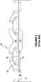
- Fig. 2 illustrates an alternate split gate memory cell 30 with same elements as memory cell 10, but additionally with a program/erase (PE) gate 32 disposed over and insulated from the source region 14 (i.e. this is a three gate design).
- Memory cell 30 can be erased by placing a high voltage on the PE gate 32 to induce tunneling of electrons from the floating gate 20 to the PE gate 32.
- Memory cell 30 can be programmed by placing positive voltages on the control gate 22, PE gate 32 and source region 14, and a current on drain region 16, to inject electrons from the current flowing through the channel region 18 onto floating gate 20.
- Memory cell 30 can be read by placing positive voltages on the control gate 22 and drain region 16, and sensing current flow.
- Fig. 3 illustrates an alternate split gate memory cell 40 with same elements as memory cell 10, but additionally with an erase gate 42 disposed over and insulated from the source region 14, and a coupling gate 44 over and insulated from the floating gate 20.
- Memory cell 40 can be erased by placing a high voltage on the erase gate 42 (and optionally a negative voltage on the coupling gate 44) to induce tunneling of electrons from the floating gate 20 to the erase gate 42.
- Memory cell 40 can be programmed by placing positive voltages on the control gate 22, erase gate 42, coupling gate 44 and source region 14, and a current on drain region 16, to inject electrons from the current flowing through the channel region 18 onto floating gate 20.
- Memory cell 40 can be read by placing positive voltages on the control gate 22 and drain region 16 (and optionally on the erase gate 42 and/or the coupling gate 44), and sensing current flow.
- each memory cell can only store one bit of data (i.e., the cell has only two possible states). There is a need to program more than one bit of data in each memory cell. It is also known to operate the above described memory cells in an analog fashion so that the memory cell can store more than just two binary values (i.e., just one bit of information).
- the memory cells can be operated below their threshold voltage, meaning that instead of fully programming or fully erasing the memory cells, they can be only partially programmed or partially erased, and operated in an analog fashion below the threshold voltage of the memory cell. It is also possible to program the memory cells to one of multiple program states above the threshold voltage too. However, if discrete programming states are desired, it can be difficult to reliably program and read the memory cells because the read current values for the various states are so close together.
- US 2014/241039 A1 discloses an electronic device including a semiconductor memory.
- the semiconductor memory includes a plurality of variable resistance elements, a plurality of read voltage application terminals configured to supply different levels of read voltages to respective one ends of the plurality of variable resistance elements, and an analog-to-digital conversion unit configured to generate multi-bit digital data corresponding to a total current which is acquired by summing currents flowing through the plurality of variable resistance elements.
- US 2012/250400 A1 discloses that the control circuit selects, as the first reference cell, a first memory cell having a maximum reading current supplied by turning on the first select transistor in a state in which resistance values of the first memory cells are all increased.
- the control circuit selects, as a second reference cell, the second memory cell having a maximum reading current supplied by turning on the second select transistor in a state in which resistance values of the second memory cells are all increased.
- the first reference-current setting circuit sets, as the first reference current, a current obtained by adding a first adjusting current to the reading current of the first reference cell.
- the second reference-current setting circuit sets, as the second reference current, a current obtained by adding a second adjusting current to the reading current of the second reference cell.
- a method of reading a memory device having a plurality of memory cells includes reading a first memory cell of the plurality of memory cells to generate a first read current, reading a second memory cell of the plurality of memory cells to generate a second read current, applying a first offset value to the second read current, and then adding the first and second read currents to form a third read current, and then determining a program state using the third read current, wherein the program state corresponds to a bit stored over at least the first and second memory cells.
- a method of reading a memory device having a plurality of memory cells includes reading a first memory cell of the plurality of memory cells to generate a first read current, reading a second memory cell of the plurality of memory cells to generate a second read current, generating a first voltage from the first read current, generating a second voltage from the second read current, applying a first offset value to the second voltage, and then adding the first and second voltages to form a third voltage, and then determining a program state using the third voltage, wherein the program state corresponds to a bit stored over at least the first and second memory cells.
- a memory device includes a semiconductor substrate, a plurality of memory cells formed on the semiconductor substrate, and circuitry formed on the semiconductor substrate and configured to read a first memory cell of the plurality of memory cells to generate a first read current, read a second memory cell of the plurality of memory cells to generate a second read current, apply a first offset value to the second read current, and then add the first and second read currents to form a third read current, and then determine a program state using the third read current, wherein the program state corresponds to a bit stored over at least the first and second memory cells.
- a memory device includes a semiconductor substrate, a plurality of memory cells formed on the semiconductor substrate, and circuitry formed on the semiconductor substrate and configured to read a first memory cell of the plurality of memory cells to generate a first read current, read a second memory cell of the plurality of memory cells to generate a second read current, generate a first voltage from the first read current, generate a second voltage from the second read current, apply a first offset value to the second voltage, and then add the first and second voltages to form a third voltage, and then determine a program state using the third voltage, wherein the program state corresponds to a bit stored over at least the first and second memory cells.
- the present invention is directed to non-volatile memory devices capable of storing more than one bit of information in each memory cell. This can be done by operating the memory cells above and/or below their threshold voltage. For example, instead of fully programming or fully erasing the memory cells, they can be only partially programmed or partially erased, and operated in an analog fashion. The following description focuses on memory cells operating below the threshold voltage of the memory cell. However, it equally applies to memory cells operated above the threshold voltage of the memory cell as well.
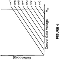
- the sub-threshold relationship between channel current as a function of control gate voltage is described.
- the channel current gradually rises.
- this relationship is linear.
- the memory cell programming state is changed (e.g., as the number of electrons programmed onto the floating gate changes)
- the linear logarithmic relationship of current as a function of control gate voltage shifts up and down.
- Fig. 4 The linear logarithmic relationship of current (through the channel region) as a function of control gate voltage is represented for multiple different program states.
- the memory cell represented by Fig. 4 can theoretically store multiple bits of information, because it can be programmed into 8 different states. By measuring the current at one or more specific control gate voltages, such as read voltage V R , the program state n can be determined.
- n program states As indicated in Fig. 4 is that the difference in read current for two adjacent program states can be too small (i.e., the program states are too close together) for reliable operation when the number of states n exceeds just a few.
- Program states too close together are susceptible to noise on the program and/or reading of the memory cells. For example, there would be a small range of variation in terms of how reliably the memory cell can be programmed into any given program state. Similarly, there would be a small range of variation in terms of how reliably the state of the cell can be read by measuring the read currents. Therefore, the n states cannot be located too close to each other, otherwise they could not reliably be distinguished from each other. This places a practical limit on the number of states n that can be programmed into a single memory cell, which means there is a practical limit on the number of states n that can be stored in the memory device.
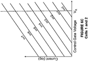
- Figures 5A-5B illustrate a solution to the above described problem.
- the different states n can be stored over multiple memory cells.
- the same number of total states can be stored, but with twice the separation between adjacent program states for better reliability.
- twice as many states can be stored with a given separation between adjacent program states using two memory cells relative to using just a single cell.
- an offset X is applied to the read current from cell 2, so that the read current readings from cell 2 are effectively shifted above any of the possible current readings from cell 1.
- the read currents for both cells for all the possible program states are collectively shown in Fig. 6C .
- Implementing the offset X for cell 2 can be done using an adding circuit that adds a current offset X to the read current from cell 2 before the read current from cell 2 is added to the cell current from cell 1 (e.g., the adding circuit is part of the sense amplifier that is used to detect currents through the cells). Or, the adding circuit can add a voltage offset X to a voltage signal that is generated by the sense amplifier to reflect the current being detected through cell 2. In this case, it would be the voltages signals (corresponding to the detected current levels) that are added together before determining from the combined voltage signal which program state was read from the pair of memory cells.
- a multiplier circuit can be as part of, or downstream of, the sense amplifier to multiply the current or voltage signal for cell 2 before being added to the current/voltage signal for cell 1.
- the offset X whether it be a voltage offset or a current offset, could be stored in a reference cell (i.e., a memory cell in the memory cell array dedicated for this purpose), so that the proper amount of offset is reliably applied to the voltage or current signal for cell 2 for that given die.
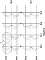
- the architecture of an exemplary memory device is illustrated in Fig. 7 .
- the memory device includes an array 50 of non-volatile memory cells, which can be segregated into two separate planes (Plane A 52a and Plane B 52b).
- the memory cells can be of the type shown in Figures 1-3 , formed on a single chip, arranged in a plurality of rows and columns in the semiconductor substrate 12. Adjacent to the array of non-volatile memory cells are address decoders (e.g.
- XDEC 54 (row decoder), SLDRV 56, YMUX 58 (column decoder), HVDEC 60) and a bit line controller (BLINHCTL 62), which are used to decode addresses and supply the various voltages to the various memory cell gates and regions during read, program, and erase operations for selected memory cells.
- Column decoder 58 includes sense amplifiers for measuring the voltages or currents on the bit lines during a read operation.
- Controller 66 (containing control circuitry) controls the various device elements to implement each operation (program, erase, read) on target memory cells.
- Charge pump CHRGPMP 64 provides the various voltages used to read, program and erase the memory cells under the control of the controller 66.
- the offset X and signal adding can be implemented, for example, with circuitry in the controller 66. Alternately or additionally, the offset X and signal adding can be implemented with circuitry in the sense amplifier portion of the column decoder YMUX 58.
- Fig. 8 shows the array configuration for the two-gate memory cells of Fig. 1 , where the memory cells are arranged in rows and columns. This array configuration equally applies to the memory cells of Figs. 2-3 , whereby additional lines would be added for the additional gates.
- Word lines WL each connect to the control gates for one row of memory cells.
- Bit lines BL each connect to the drain regions for one column of memory cells.
- Source lines SL each connect to the source regions for one row of a pair of memory cells.
- each of cells having their read currents or voltages added together are disposed in different columns so the read process is faster. Therefore, for the example above where two memory cells are used, cell 1 would be in column 1 connected to bit line BL0, and cell 2 would be in column 2 connected to bit line BL1.
- the read current for cell 1 is detected on bit line BL0 and the read current for cell 2 is detected on bit line BL1.
- Circuitry in the sense amplifiers or downstream from there will add the offset X to the read current on bit line BL1 (or the voltage corresponding thereto) and then add the read currents (or voltages) from both cells to each other and then determine from the combined read current/voltage what program state is programmed in the pair of memory cells.
- offset X could include a negative offset, which can be achieved by subtracting from (decreasing) the value of the current or voltage by the amount X.
- Materials, processes and numerical examples described above are exemplary only, and should not be deemed to limit the claims. Further, as is apparent from the claims and specification, not all method steps need be performed in the exact order illustrated. Lastly, single layers of material could be formed as multiple layers of such or similar materials, and vice versa.
- the term “adjacent” includes “directly adjacent” (no intermediate materials, elements or space disposed therebetween) and “indirectly adjacent” (intermediate materials, elements or space disposed there between), “mounted to” includes “directly mounted to” (no intermediate materials, elements or space disposed there between) and “indirectly mounted to” (intermediate materials, elements or spaced disposed there between), and “electrically coupled” includes “directly electrically coupled to” (no intermediate materials or elements there between that electrically connect the elements together) and “indirectly electrically coupled to” (intermediate materials or elements there between that electrically connect the elements together).
- forming an element "over a substrate” can include forming the element directly on the substrate with no intermediate materials/elements therebetween, as well as forming the element indirectly on the substrate with one or more intermediate materials/elements therebetween.
Landscapes
- Engineering & Computer Science (AREA)
- Microelectronics & Electronic Packaging (AREA)
- Computer Hardware Design (AREA)
- Read Only Memory (AREA)
- Semiconductor Memories (AREA)
- Non-Volatile Memory (AREA)
Applications Claiming Priority (3)
| Application Number | Priority Date | Filing Date | Title |
|---|---|---|---|
| US201762581489P | 2017-11-03 | 2017-11-03 | |
| US16/148,304 US10515694B2 (en) | 2017-11-03 | 2018-10-01 | System and method for storing multibit data in non-volatile memory |
| PCT/US2018/053930 WO2019089168A1 (en) | 2017-11-03 | 2018-10-02 | System and method for storing multibit data in non-volatile memory |
Publications (3)
| Publication Number | Publication Date |
|---|---|
| EP3704700A1 EP3704700A1 (en) | 2020-09-09 |
| EP3704700A4 EP3704700A4 (en) | 2021-07-21 |
| EP3704700B1 true EP3704700B1 (en) | 2022-07-20 |
Family
ID=66327523
Family Applications (1)
| Application Number | Title | Priority Date | Filing Date |
|---|---|---|---|
| EP18872824.0A Active EP3704700B1 (en) | 2017-11-03 | 2018-10-02 | System and method for storing multibit data in non-volatile memory |
Country Status (7)
| Country | Link |
|---|---|
| US (1) | US10515694B2 (enExample) |
| EP (1) | EP3704700B1 (enExample) |
| JP (1) | JP6970826B2 (enExample) |
| KR (1) | KR102199607B1 (enExample) |
| CN (1) | CN111344791B (enExample) |
| TW (1) | TWI682393B (enExample) |
| WO (1) | WO2019089168A1 (enExample) |
Families Citing this family (6)
| Publication number | Priority date | Publication date | Assignee | Title |
|---|---|---|---|---|
| KR100671698B1 (ko) * | 2004-08-05 | 2007-01-18 | 매그나칩 반도체 유한회사 | 엘디아이 내 디지털 아날로그 변환기의 테스트 장치 |
| US10991433B2 (en) * | 2019-09-03 | 2021-04-27 | Silicon Storage Technology, Inc. | Method of improving read current stability in analog non-volatile memory by limiting time gap between erase and program |
| US11682459B2 (en) * | 2020-05-13 | 2023-06-20 | Silicon Storage Technology, Inc. | Analog neural memory array in artificial neural network comprising logical cells and improved programming mechanism |
| US12080355B2 (en) | 2021-06-02 | 2024-09-03 | Silicon Storage Technology, Inc. | Method of improving read current stability in analog non-volatile memory by post-program tuning for memory cells exhibiting random telegraph noise |
| US11769558B2 (en) * | 2021-06-08 | 2023-09-26 | Silicon Storage Technology, Inc. | Method of reducing random telegraph noise in non-volatile memory by grouping and screening memory cells |
| KR102703459B1 (ko) | 2021-11-29 | 2024-09-06 | 충남대학교 산학협력단 | 멀티 레벨 구동이 가능한 메모리 소자 |
Family Cites Families (17)
| Publication number | Priority date | Publication date | Assignee | Title |
|---|---|---|---|---|
| US5029130A (en) | 1990-01-22 | 1991-07-02 | Silicon Storage Technology, Inc. | Single transistor non-valatile electrically alterable semiconductor memory device |
| JP2812202B2 (ja) * | 1994-06-27 | 1998-10-22 | ヤマハ株式会社 | 半導体記憶装置 |
| KR100324594B1 (ko) | 1999-06-28 | 2002-02-16 | 박종섭 | 강유전체 메모리 장치 |
| US7082056B2 (en) | 2004-03-12 | 2006-07-25 | Super Talent Electronics, Inc. | Flash memory device and architecture with multi level cells |
| US7324374B2 (en) | 2003-06-20 | 2008-01-29 | Spansion Llc | Memory with a core-based virtual ground and dynamic reference sensing scheme |
| US7315056B2 (en) | 2004-06-07 | 2008-01-01 | Silicon Storage Technology, Inc. | Semiconductor memory array of floating gate memory cells with program/erase and select gates |
| US7554856B2 (en) * | 2006-10-06 | 2009-06-30 | Qimonda Flash Gmbh & Co. Kg | Memory cell |
| US20090039410A1 (en) | 2007-08-06 | 2009-02-12 | Xian Liu | Split Gate Non-Volatile Flash Memory Cell Having A Floating Gate, Control Gate, Select Gate And An Erase Gate With An Overhang Over The Floating Gate, Array And Method Of Manufacturing |
| US8238149B2 (en) | 2009-06-25 | 2012-08-07 | Macronix International Co., Ltd. | Methods and apparatus for reducing defect bits in phase change memory |
| JP2012209004A (ja) | 2011-03-30 | 2012-10-25 | Toshiba Corp | 半導体記憶装置 |
| US9099202B2 (en) * | 2012-11-06 | 2015-08-04 | Sandisk Technologies Inc. | 3D stacked non-volatile storage programming to conductive state |
| KR102043723B1 (ko) | 2013-02-28 | 2019-12-02 | 에스케이하이닉스 주식회사 | 반도체 장치 및 이를 포함하는 프로세서와 시스템 |
| KR101716998B1 (ko) | 2013-03-14 | 2017-03-15 | 실리콘 스토리지 테크놀로지 인크 | 비휘발성 메모리 프로그램 알고리즘 디바이스 및 방법 |
| US20150085571A1 (en) * | 2013-09-24 | 2015-03-26 | Sandisk Technologies Inc. | Updating read voltages |
| US9543041B2 (en) * | 2014-08-29 | 2017-01-10 | Everspin Technologies, Inc. | Configuration and testing for magnetoresistive memory to ensure long term continuous operation |
| US9905302B2 (en) * | 2014-11-20 | 2018-02-27 | Western Digital Technologies, Inc. | Read level grouping algorithms for increased flash performance |
| US9484094B2 (en) | 2015-01-21 | 2016-11-01 | Ememory Technology Inc. | Control method of resistive random-access memory |
-
2018
- 2018-10-01 US US16/148,304 patent/US10515694B2/en active Active
- 2018-10-02 WO PCT/US2018/053930 patent/WO2019089168A1/en not_active Ceased
- 2018-10-02 KR KR1020207010818A patent/KR102199607B1/ko active Active
- 2018-10-02 EP EP18872824.0A patent/EP3704700B1/en active Active
- 2018-10-02 JP JP2020524440A patent/JP6970826B2/ja active Active
- 2018-10-02 CN CN201880068646.XA patent/CN111344791B/zh active Active
- 2018-10-24 TW TW107137607A patent/TWI682393B/zh active
Also Published As
| Publication number | Publication date |
|---|---|
| TW201931370A (zh) | 2019-08-01 |
| JP6970826B2 (ja) | 2021-11-24 |
| US20190139602A1 (en) | 2019-05-09 |
| KR102199607B1 (ko) | 2021-01-08 |
| WO2019089168A1 (en) | 2019-05-09 |
| CN111344791B (zh) | 2021-06-25 |
| TWI682393B (zh) | 2020-01-11 |
| JP2021501956A (ja) | 2021-01-21 |
| CN111344791A (zh) | 2020-06-26 |
| EP3704700A4 (en) | 2021-07-21 |
| US10515694B2 (en) | 2019-12-24 |
| KR20200043501A (ko) | 2020-04-27 |
| EP3704700A1 (en) | 2020-09-09 |
Similar Documents
| Publication | Publication Date | Title |
|---|---|---|
| EP3704700B1 (en) | System and method for storing multibit data in non-volatile memory | |
| EP4026129B1 (en) | Method of improving read current stability in analog non-volatile memory by screening memory cells | |
| US10699787B2 (en) | System and method for minimizing floating gate to floating gate coupling effects during programming in flash memory | |
| US10878897B2 (en) | System and method for storing and retrieving multibit data in non-volatile memory using current multipliers | |
| KR102282580B1 (ko) | 비휘발성 메모리 어레이에서 피크 전력 요구 및 잡음을 관리하기 위한 시스템 및 방법 | |
| EP3665679A1 (en) | System and method for implementing inference engine by optimizing programming operation | |
| US20250231705A1 (en) | Coarse and fine programming of non-volatile memory cells | |
| US20250285684A1 (en) | Sequential erase for tuning the program state of non-volatile memory cells | |
| US20250181255A1 (en) | Program speed compensation for non-volatile memory cells | |
| US20250190125A1 (en) | Accelerated programming of four gate, split-gate flash memory cells | |
| WO2025151138A1 (en) | Coarse and fine programming of non-volatile memory cells | |
| WO2025188339A1 (en) | Sequential erase for tuning the program state of non-volatile memory cells | |
| WO2025122184A1 (en) | Accelerated programming of four-gate, split-gate flash memory cells |
Legal Events
| Date | Code | Title | Description |
|---|---|---|---|
| STAA | Information on the status of an ep patent application or granted ep patent |
Free format text: STATUS: THE INTERNATIONAL PUBLICATION HAS BEEN MADE |
|
| PUAI | Public reference made under article 153(3) epc to a published international application that has entered the european phase |
Free format text: ORIGINAL CODE: 0009012 |
|
| STAA | Information on the status of an ep patent application or granted ep patent |
Free format text: STATUS: REQUEST FOR EXAMINATION WAS MADE |
|
| 17P | Request for examination filed |
Effective date: 20200603 |
|
| AK | Designated contracting states |
Kind code of ref document: A1 Designated state(s): AL AT BE BG CH CY CZ DE DK EE ES FI FR GB GR HR HU IE IS IT LI LT LU LV MC MK MT NL NO PL PT RO RS SE SI SK SM TR |
|
| AX | Request for extension of the european patent |
Extension state: BA ME |
|
| DAV | Request for validation of the european patent (deleted) | ||
| DAX | Request for extension of the european patent (deleted) | ||
| A4 | Supplementary search report drawn up and despatched |
Effective date: 20210618 |
|
| RIC1 | Information provided on ipc code assigned before grant |
Ipc: G11C 11/56 20060101AFI20210614BHEP Ipc: G11C 16/26 20060101ALI20210614BHEP |
|
| REG | Reference to a national code |
Ref country code: DE Ref legal event code: R079 Ref document number: 602018038293 Country of ref document: DE Free format text: PREVIOUS MAIN CLASS: G11C0013000000 Ipc: G11C0011560000 |
|
| GRAP | Despatch of communication of intention to grant a patent |
Free format text: ORIGINAL CODE: EPIDOSNIGR1 |
|
| STAA | Information on the status of an ep patent application or granted ep patent |
Free format text: STATUS: GRANT OF PATENT IS INTENDED |
|
| RIC1 | Information provided on ipc code assigned before grant |
Ipc: G11C 16/04 20060101ALI20220310BHEP Ipc: G11C 16/26 20060101ALI20220310BHEP Ipc: G11C 11/56 20060101AFI20220310BHEP |
|
| INTG | Intention to grant announced |
Effective date: 20220407 |
|
| GRAS | Grant fee paid |
Free format text: ORIGINAL CODE: EPIDOSNIGR3 |
|
| GRAA | (expected) grant |
Free format text: ORIGINAL CODE: 0009210 |
|
| STAA | Information on the status of an ep patent application or granted ep patent |
Free format text: STATUS: THE PATENT HAS BEEN GRANTED |
|
| AK | Designated contracting states |
Kind code of ref document: B1 Designated state(s): AL AT BE BG CH CY CZ DE DK EE ES FI FR GB GR HR HU IE IS IT LI LT LU LV MC MK MT NL NO PL PT RO RS SE SI SK SM TR |
|
| REG | Reference to a national code |
Ref country code: CH Ref legal event code: EP |
|
| REG | Reference to a national code |
Ref country code: DE Ref legal event code: R096 Ref document number: 602018038293 Country of ref document: DE |
|
| REG | Reference to a national code |
Ref country code: AT Ref legal event code: REF Ref document number: 1506063 Country of ref document: AT Kind code of ref document: T Effective date: 20220815 |
|
| REG | Reference to a national code |
Ref country code: IE Ref legal event code: FG4D |
|
| REG | Reference to a national code |
Ref country code: NL Ref legal event code: FP |
|
| REG | Reference to a national code |
Ref country code: LT Ref legal event code: MG9D |
|
| PG25 | Lapsed in a contracting state [announced via postgrant information from national office to epo] |
Ref country code: SE Free format text: LAPSE BECAUSE OF FAILURE TO SUBMIT A TRANSLATION OF THE DESCRIPTION OR TO PAY THE FEE WITHIN THE PRESCRIBED TIME-LIMIT Effective date: 20220720 Ref country code: RS Free format text: LAPSE BECAUSE OF FAILURE TO SUBMIT A TRANSLATION OF THE DESCRIPTION OR TO PAY THE FEE WITHIN THE PRESCRIBED TIME-LIMIT Effective date: 20220720 Ref country code: PT Free format text: LAPSE BECAUSE OF FAILURE TO SUBMIT A TRANSLATION OF THE DESCRIPTION OR TO PAY THE FEE WITHIN THE PRESCRIBED TIME-LIMIT Effective date: 20221121 Ref country code: NO Free format text: LAPSE BECAUSE OF FAILURE TO SUBMIT A TRANSLATION OF THE DESCRIPTION OR TO PAY THE FEE WITHIN THE PRESCRIBED TIME-LIMIT Effective date: 20221020 Ref country code: LV Free format text: LAPSE BECAUSE OF FAILURE TO SUBMIT A TRANSLATION OF THE DESCRIPTION OR TO PAY THE FEE WITHIN THE PRESCRIBED TIME-LIMIT Effective date: 20220720 Ref country code: LT Free format text: LAPSE BECAUSE OF FAILURE TO SUBMIT A TRANSLATION OF THE DESCRIPTION OR TO PAY THE FEE WITHIN THE PRESCRIBED TIME-LIMIT Effective date: 20220720 Ref country code: FI Free format text: LAPSE BECAUSE OF FAILURE TO SUBMIT A TRANSLATION OF THE DESCRIPTION OR TO PAY THE FEE WITHIN THE PRESCRIBED TIME-LIMIT Effective date: 20220720 Ref country code: ES Free format text: LAPSE BECAUSE OF FAILURE TO SUBMIT A TRANSLATION OF THE DESCRIPTION OR TO PAY THE FEE WITHIN THE PRESCRIBED TIME-LIMIT Effective date: 20220720 |
|
| REG | Reference to a national code |
Ref country code: AT Ref legal event code: MK05 Ref document number: 1506063 Country of ref document: AT Kind code of ref document: T Effective date: 20220720 |
|
| PG25 | Lapsed in a contracting state [announced via postgrant information from national office to epo] |
Ref country code: PL Free format text: LAPSE BECAUSE OF FAILURE TO SUBMIT A TRANSLATION OF THE DESCRIPTION OR TO PAY THE FEE WITHIN THE PRESCRIBED TIME-LIMIT Effective date: 20220720 Ref country code: IS Free format text: LAPSE BECAUSE OF FAILURE TO SUBMIT A TRANSLATION OF THE DESCRIPTION OR TO PAY THE FEE WITHIN THE PRESCRIBED TIME-LIMIT Effective date: 20221120 Ref country code: HR Free format text: LAPSE BECAUSE OF FAILURE TO SUBMIT A TRANSLATION OF THE DESCRIPTION OR TO PAY THE FEE WITHIN THE PRESCRIBED TIME-LIMIT Effective date: 20220720 Ref country code: GR Free format text: LAPSE BECAUSE OF FAILURE TO SUBMIT A TRANSLATION OF THE DESCRIPTION OR TO PAY THE FEE WITHIN THE PRESCRIBED TIME-LIMIT Effective date: 20221021 |
|
| REG | Reference to a national code |
Ref country code: DE Ref legal event code: R097 Ref document number: 602018038293 Country of ref document: DE |
|
| PG25 | Lapsed in a contracting state [announced via postgrant information from national office to epo] |
Ref country code: SM Free format text: LAPSE BECAUSE OF FAILURE TO SUBMIT A TRANSLATION OF THE DESCRIPTION OR TO PAY THE FEE WITHIN THE PRESCRIBED TIME-LIMIT Effective date: 20220720 Ref country code: RO Free format text: LAPSE BECAUSE OF FAILURE TO SUBMIT A TRANSLATION OF THE DESCRIPTION OR TO PAY THE FEE WITHIN THE PRESCRIBED TIME-LIMIT Effective date: 20220720 Ref country code: DK Free format text: LAPSE BECAUSE OF FAILURE TO SUBMIT A TRANSLATION OF THE DESCRIPTION OR TO PAY THE FEE WITHIN THE PRESCRIBED TIME-LIMIT Effective date: 20220720 Ref country code: CZ Free format text: LAPSE BECAUSE OF FAILURE TO SUBMIT A TRANSLATION OF THE DESCRIPTION OR TO PAY THE FEE WITHIN THE PRESCRIBED TIME-LIMIT Effective date: 20220720 Ref country code: AT Free format text: LAPSE BECAUSE OF FAILURE TO SUBMIT A TRANSLATION OF THE DESCRIPTION OR TO PAY THE FEE WITHIN THE PRESCRIBED TIME-LIMIT Effective date: 20220720 |
|
| PLBE | No opposition filed within time limit |
Free format text: ORIGINAL CODE: 0009261 |
|
| STAA | Information on the status of an ep patent application or granted ep patent |
Free format text: STATUS: NO OPPOSITION FILED WITHIN TIME LIMIT |
|
| PG25 | Lapsed in a contracting state [announced via postgrant information from national office to epo] |
Ref country code: SK Free format text: LAPSE BECAUSE OF FAILURE TO SUBMIT A TRANSLATION OF THE DESCRIPTION OR TO PAY THE FEE WITHIN THE PRESCRIBED TIME-LIMIT Effective date: 20220720 Ref country code: MC Free format text: LAPSE BECAUSE OF FAILURE TO SUBMIT A TRANSLATION OF THE DESCRIPTION OR TO PAY THE FEE WITHIN THE PRESCRIBED TIME-LIMIT Effective date: 20220720 Ref country code: EE Free format text: LAPSE BECAUSE OF FAILURE TO SUBMIT A TRANSLATION OF THE DESCRIPTION OR TO PAY THE FEE WITHIN THE PRESCRIBED TIME-LIMIT Effective date: 20220720 |
|
| REG | Reference to a national code |
Ref country code: CH Ref legal event code: PL |
|
| REG | Reference to a national code |
Ref country code: BE Ref legal event code: MM Effective date: 20221031 |
|
| 26N | No opposition filed |
Effective date: 20230421 |
|
| GBPC | Gb: european patent ceased through non-payment of renewal fee |
Effective date: 20221020 |
|
| PG25 | Lapsed in a contracting state [announced via postgrant information from national office to epo] |
Ref country code: LU Free format text: LAPSE BECAUSE OF NON-PAYMENT OF DUE FEES Effective date: 20221002 Ref country code: AL Free format text: LAPSE BECAUSE OF FAILURE TO SUBMIT A TRANSLATION OF THE DESCRIPTION OR TO PAY THE FEE WITHIN THE PRESCRIBED TIME-LIMIT Effective date: 20220720 |
|
| P01 | Opt-out of the competence of the unified patent court (upc) registered |
Effective date: 20230528 |
|
| PG25 | Lapsed in a contracting state [announced via postgrant information from national office to epo] |
Ref country code: LI Free format text: LAPSE BECAUSE OF NON-PAYMENT OF DUE FEES Effective date: 20221031 Ref country code: CH Free format text: LAPSE BECAUSE OF NON-PAYMENT OF DUE FEES Effective date: 20221031 |
|
| PG25 | Lapsed in a contracting state [announced via postgrant information from national office to epo] |
Ref country code: SI Free format text: LAPSE BECAUSE OF FAILURE TO SUBMIT A TRANSLATION OF THE DESCRIPTION OR TO PAY THE FEE WITHIN THE PRESCRIBED TIME-LIMIT Effective date: 20220720 |
|
| PG25 | Lapsed in a contracting state [announced via postgrant information from national office to epo] |
Ref country code: BE Free format text: LAPSE BECAUSE OF NON-PAYMENT OF DUE FEES Effective date: 20221031 |
|
| PG25 | Lapsed in a contracting state [announced via postgrant information from national office to epo] |
Ref country code: IE Free format text: LAPSE BECAUSE OF NON-PAYMENT OF DUE FEES Effective date: 20221002 Ref country code: GB Free format text: LAPSE BECAUSE OF NON-PAYMENT OF DUE FEES Effective date: 20221020 |
|
| PG25 | Lapsed in a contracting state [announced via postgrant information from national office to epo] |
Ref country code: CY Free format text: LAPSE BECAUSE OF FAILURE TO SUBMIT A TRANSLATION OF THE DESCRIPTION OR TO PAY THE FEE WITHIN THE PRESCRIBED TIME-LIMIT Effective date: 20220720 |
|
| PG25 | Lapsed in a contracting state [announced via postgrant information from national office to epo] |
Ref country code: MK Free format text: LAPSE BECAUSE OF FAILURE TO SUBMIT A TRANSLATION OF THE DESCRIPTION OR TO PAY THE FEE WITHIN THE PRESCRIBED TIME-LIMIT Effective date: 20220720 Ref country code: IT Free format text: LAPSE BECAUSE OF FAILURE TO SUBMIT A TRANSLATION OF THE DESCRIPTION OR TO PAY THE FEE WITHIN THE PRESCRIBED TIME-LIMIT Effective date: 20220720 Ref country code: HU Free format text: LAPSE BECAUSE OF FAILURE TO SUBMIT A TRANSLATION OF THE DESCRIPTION OR TO PAY THE FEE WITHIN THE PRESCRIBED TIME-LIMIT; INVALID AB INITIO Effective date: 20181002 |
|
| PG25 | Lapsed in a contracting state [announced via postgrant information from national office to epo] |
Ref country code: BG Free format text: LAPSE BECAUSE OF FAILURE TO SUBMIT A TRANSLATION OF THE DESCRIPTION OR TO PAY THE FEE WITHIN THE PRESCRIBED TIME-LIMIT Effective date: 20220720 |
|
| PG25 | Lapsed in a contracting state [announced via postgrant information from national office to epo] |
Ref country code: MT Free format text: LAPSE BECAUSE OF FAILURE TO SUBMIT A TRANSLATION OF THE DESCRIPTION OR TO PAY THE FEE WITHIN THE PRESCRIBED TIME-LIMIT Effective date: 20220720 |
|
| PGFP | Annual fee paid to national office [announced via postgrant information from national office to epo] |
Ref country code: DE Payment date: 20240919 Year of fee payment: 7 |
|
| PGFP | Annual fee paid to national office [announced via postgrant information from national office to epo] |
Ref country code: NL Payment date: 20250923 Year of fee payment: 8 |
|
| PGFP | Annual fee paid to national office [announced via postgrant information from national office to epo] |
Ref country code: FR Payment date: 20250924 Year of fee payment: 8 |