EP3702834A1 - Arraysubstrat und anzeigevorrichtung - Google Patents
Arraysubstrat und anzeigevorrichtung Download PDFInfo
- Publication number
- EP3702834A1 EP3702834A1 EP18869964.9A EP18869964A EP3702834A1 EP 3702834 A1 EP3702834 A1 EP 3702834A1 EP 18869964 A EP18869964 A EP 18869964A EP 3702834 A1 EP3702834 A1 EP 3702834A1
- Authority
- EP
- European Patent Office
- Prior art keywords
- sub
- array substrate
- electrodes
- common
- pixel
- Prior art date
- Legal status (The legal status is an assumption and is not a legal conclusion. Google has not performed a legal analysis and makes no representation as to the accuracy of the status listed.)
- Granted
Links
Images


Classifications
-
- G—PHYSICS
- G02—OPTICS
- G02F—OPTICAL DEVICES OR ARRANGEMENTS FOR THE CONTROL OF LIGHT BY MODIFICATION OF THE OPTICAL PROPERTIES OF THE MEDIA OF THE ELEMENTS INVOLVED THEREIN; NON-LINEAR OPTICS; FREQUENCY-CHANGING OF LIGHT; OPTICAL LOGIC ELEMENTS; OPTICAL ANALOGUE/DIGITAL CONVERTERS
- G02F1/00—Devices or arrangements for the control of the intensity, colour, phase, polarisation or direction of light arriving from an independent light source, e.g. switching, gating or modulating; Non-linear optics
- G02F1/01—Devices or arrangements for the control of the intensity, colour, phase, polarisation or direction of light arriving from an independent light source, e.g. switching, gating or modulating; Non-linear optics for the control of the intensity, phase, polarisation or colour
- G02F1/13—Devices or arrangements for the control of the intensity, colour, phase, polarisation or direction of light arriving from an independent light source, e.g. switching, gating or modulating; Non-linear optics for the control of the intensity, phase, polarisation or colour based on liquid crystals, e.g. single liquid crystal display cells
- G02F1/133—Constructional arrangements; Operation of liquid crystal cells; Circuit arrangements
- G02F1/1333—Constructional arrangements; Manufacturing methods
- G02F1/1343—Electrodes
- G02F1/134309—Electrodes characterised by their geometrical arrangement
-
- H—ELECTRICITY
- H10—SEMICONDUCTOR DEVICES; ELECTRIC SOLID-STATE DEVICES NOT OTHERWISE PROVIDED FOR
- H10D—INORGANIC ELECTRIC SEMICONDUCTOR DEVICES
- H10D86/00—Integrated devices formed in or on insulating or conducting substrates, e.g. formed in silicon-on-insulator [SOI] substrates or on stainless steel or glass substrates
- H10D86/40—Integrated devices formed in or on insulating or conducting substrates, e.g. formed in silicon-on-insulator [SOI] substrates or on stainless steel or glass substrates characterised by multiple TFTs
- H10D86/60—Integrated devices formed in or on insulating or conducting substrates, e.g. formed in silicon-on-insulator [SOI] substrates or on stainless steel or glass substrates characterised by multiple TFTs wherein the TFTs are in active matrices
-
- G—PHYSICS
- G02—OPTICS
- G02F—OPTICAL DEVICES OR ARRANGEMENTS FOR THE CONTROL OF LIGHT BY MODIFICATION OF THE OPTICAL PROPERTIES OF THE MEDIA OF THE ELEMENTS INVOLVED THEREIN; NON-LINEAR OPTICS; FREQUENCY-CHANGING OF LIGHT; OPTICAL LOGIC ELEMENTS; OPTICAL ANALOGUE/DIGITAL CONVERTERS
- G02F1/00—Devices or arrangements for the control of the intensity, colour, phase, polarisation or direction of light arriving from an independent light source, e.g. switching, gating or modulating; Non-linear optics
- G02F1/01—Devices or arrangements for the control of the intensity, colour, phase, polarisation or direction of light arriving from an independent light source, e.g. switching, gating or modulating; Non-linear optics for the control of the intensity, phase, polarisation or colour
- G02F1/13—Devices or arrangements for the control of the intensity, colour, phase, polarisation or direction of light arriving from an independent light source, e.g. switching, gating or modulating; Non-linear optics for the control of the intensity, phase, polarisation or colour based on liquid crystals, e.g. single liquid crystal display cells
- G02F1/133—Constructional arrangements; Operation of liquid crystal cells; Circuit arrangements
- G02F1/136—Liquid crystal cells structurally associated with a semi-conducting layer or substrate, e.g. cells forming part of an integrated circuit
- G02F1/1362—Active matrix addressed cells
- G02F1/136218—Shield electrodes
-
- H—ELECTRICITY
- H10—SEMICONDUCTOR DEVICES; ELECTRIC SOLID-STATE DEVICES NOT OTHERWISE PROVIDED FOR
- H10D—INORGANIC ELECTRIC SEMICONDUCTOR DEVICES
- H10D86/00—Integrated devices formed in or on insulating or conducting substrates, e.g. formed in silicon-on-insulator [SOI] substrates or on stainless steel or glass substrates
- H10D86/40—Integrated devices formed in or on insulating or conducting substrates, e.g. formed in silicon-on-insulator [SOI] substrates or on stainless steel or glass substrates characterised by multiple TFTs
- H10D86/441—Interconnections, e.g. scanning lines
- H10D86/443—Interconnections, e.g. scanning lines adapted for preventing breakage, peeling or short circuiting
-
- G—PHYSICS
- G02—OPTICS
- G02F—OPTICAL DEVICES OR ARRANGEMENTS FOR THE CONTROL OF LIGHT BY MODIFICATION OF THE OPTICAL PROPERTIES OF THE MEDIA OF THE ELEMENTS INVOLVED THEREIN; NON-LINEAR OPTICS; FREQUENCY-CHANGING OF LIGHT; OPTICAL LOGIC ELEMENTS; OPTICAL ANALOGUE/DIGITAL CONVERTERS
- G02F1/00—Devices or arrangements for the control of the intensity, colour, phase, polarisation or direction of light arriving from an independent light source, e.g. switching, gating or modulating; Non-linear optics
- G02F1/01—Devices or arrangements for the control of the intensity, colour, phase, polarisation or direction of light arriving from an independent light source, e.g. switching, gating or modulating; Non-linear optics for the control of the intensity, phase, polarisation or colour
- G02F1/13—Devices or arrangements for the control of the intensity, colour, phase, polarisation or direction of light arriving from an independent light source, e.g. switching, gating or modulating; Non-linear optics for the control of the intensity, phase, polarisation or colour based on liquid crystals, e.g. single liquid crystal display cells
- G02F1/133—Constructional arrangements; Operation of liquid crystal cells; Circuit arrangements
- G02F1/1333—Constructional arrangements; Manufacturing methods
- G02F1/1337—Surface-induced orientation of the liquid crystal molecules, e.g. by alignment layers
- G02F1/133707—Structures for producing distorted electric fields, e.g. bumps, protrusions, recesses, slits in pixel electrodes
-
- G—PHYSICS
- G02—OPTICS
- G02F—OPTICAL DEVICES OR ARRANGEMENTS FOR THE CONTROL OF LIGHT BY MODIFICATION OF THE OPTICAL PROPERTIES OF THE MEDIA OF THE ELEMENTS INVOLVED THEREIN; NON-LINEAR OPTICS; FREQUENCY-CHANGING OF LIGHT; OPTICAL LOGIC ELEMENTS; OPTICAL ANALOGUE/DIGITAL CONVERTERS
- G02F1/00—Devices or arrangements for the control of the intensity, colour, phase, polarisation or direction of light arriving from an independent light source, e.g. switching, gating or modulating; Non-linear optics
- G02F1/01—Devices or arrangements for the control of the intensity, colour, phase, polarisation or direction of light arriving from an independent light source, e.g. switching, gating or modulating; Non-linear optics for the control of the intensity, phase, polarisation or colour
- G02F1/13—Devices or arrangements for the control of the intensity, colour, phase, polarisation or direction of light arriving from an independent light source, e.g. switching, gating or modulating; Non-linear optics for the control of the intensity, phase, polarisation or colour based on liquid crystals, e.g. single liquid crystal display cells
- G02F1/133—Constructional arrangements; Operation of liquid crystal cells; Circuit arrangements
- G02F1/1333—Constructional arrangements; Manufacturing methods
- G02F1/1343—Electrodes
- G02F1/134309—Electrodes characterised by their geometrical arrangement
- G02F1/134318—Electrodes characterised by their geometrical arrangement having a patterned common electrode
-
- G—PHYSICS
- G02—OPTICS
- G02F—OPTICAL DEVICES OR ARRANGEMENTS FOR THE CONTROL OF LIGHT BY MODIFICATION OF THE OPTICAL PROPERTIES OF THE MEDIA OF THE ELEMENTS INVOLVED THEREIN; NON-LINEAR OPTICS; FREQUENCY-CHANGING OF LIGHT; OPTICAL LOGIC ELEMENTS; OPTICAL ANALOGUE/DIGITAL CONVERTERS
- G02F1/00—Devices or arrangements for the control of the intensity, colour, phase, polarisation or direction of light arriving from an independent light source, e.g. switching, gating or modulating; Non-linear optics
- G02F1/01—Devices or arrangements for the control of the intensity, colour, phase, polarisation or direction of light arriving from an independent light source, e.g. switching, gating or modulating; Non-linear optics for the control of the intensity, phase, polarisation or colour
- G02F1/13—Devices or arrangements for the control of the intensity, colour, phase, polarisation or direction of light arriving from an independent light source, e.g. switching, gating or modulating; Non-linear optics for the control of the intensity, phase, polarisation or colour based on liquid crystals, e.g. single liquid crystal display cells
- G02F1/133—Constructional arrangements; Operation of liquid crystal cells; Circuit arrangements
- G02F1/1333—Constructional arrangements; Manufacturing methods
- G02F1/1343—Electrodes
- G02F1/134309—Electrodes characterised by their geometrical arrangement
- G02F1/134363—Electrodes characterised by their geometrical arrangement for applying an electric field parallel to the substrate, i.e. in-plane switching [IPS]
-
- G—PHYSICS
- G02—OPTICS
- G02F—OPTICAL DEVICES OR ARRANGEMENTS FOR THE CONTROL OF LIGHT BY MODIFICATION OF THE OPTICAL PROPERTIES OF THE MEDIA OF THE ELEMENTS INVOLVED THEREIN; NON-LINEAR OPTICS; FREQUENCY-CHANGING OF LIGHT; OPTICAL LOGIC ELEMENTS; OPTICAL ANALOGUE/DIGITAL CONVERTERS
- G02F1/00—Devices or arrangements for the control of the intensity, colour, phase, polarisation or direction of light arriving from an independent light source, e.g. switching, gating or modulating; Non-linear optics
- G02F1/01—Devices or arrangements for the control of the intensity, colour, phase, polarisation or direction of light arriving from an independent light source, e.g. switching, gating or modulating; Non-linear optics for the control of the intensity, phase, polarisation or colour
- G02F1/13—Devices or arrangements for the control of the intensity, colour, phase, polarisation or direction of light arriving from an independent light source, e.g. switching, gating or modulating; Non-linear optics for the control of the intensity, phase, polarisation or colour based on liquid crystals, e.g. single liquid crystal display cells
- G02F1/133—Constructional arrangements; Operation of liquid crystal cells; Circuit arrangements
- G02F1/1333—Constructional arrangements; Manufacturing methods
- G02F1/1343—Electrodes
- G02F1/134309—Electrodes characterised by their geometrical arrangement
- G02F1/134372—Electrodes characterised by their geometrical arrangement for fringe field switching [FFS] where the common electrode is not patterned
-
- G—PHYSICS
- G02—OPTICS
- G02F—OPTICAL DEVICES OR ARRANGEMENTS FOR THE CONTROL OF LIGHT BY MODIFICATION OF THE OPTICAL PROPERTIES OF THE MEDIA OF THE ELEMENTS INVOLVED THEREIN; NON-LINEAR OPTICS; FREQUENCY-CHANGING OF LIGHT; OPTICAL LOGIC ELEMENTS; OPTICAL ANALOGUE/DIGITAL CONVERTERS
- G02F2201/00—Constructional arrangements not provided for in groups G02F1/00 - G02F7/00
- G02F2201/12—Constructional arrangements not provided for in groups G02F1/00 - G02F7/00 electrode
- G02F2201/124—Constructional arrangements not provided for in groups G02F1/00 - G02F7/00 electrode interdigital
Definitions
- the present disclosure relates to the field of display technologies, and particularly to an array substrate and a display device.
- TFT-LCD Thin Film Transistor Liquid Crystal Display
- Common electrodes and pixel electrodes in the existing array substrate are arranged so that the resistances of the common electrodes are not uniform, thus degrading a display effect of the display panel as a whole.
- Some embodiments of this disclosure provide an array substrate including: a plurality of sub-pixel elements arranged in an array, wherein:
- two adjacent sub-common electrodes in each common electrode share a shielding section.
- each of the sub-pixel elements includes a pixel electrode
- the array substrate further includes data lines and gate lines;
- two adjacent sub-pixel elements connected with each gate line belong respectively to different rows.
- the gate lines are bent lines, and in the sub-pixel elements connected with a same gate line, the protruding connection sections of the respective pixel electrodes are arranged alternately in parallel.
- the pixel electrodes and the common electrodes are arranged at a same layer, and orthographic projections of the pixel electrodes in a direction perpendicular to the array substrate do not overlap with the orthographic projections of the common electrodes in the direction perpendicular to the array substrate.
- the electrode sections of the pixel electrodes include a plurality of second comb teeth connected with the protruding connection sections; and the second comb teeth and the first comb teeth are arranged alternately in parallel in a direction parallel to the extension direction of the gate lines.
- the pixel electrodes and the common electrodes are at different layers, and the electrode sections of the pixel electrodes are plate shape.
- the electrode sections of the pixel electrodes are structures including straight edges, and the first comb teeth of the common electrodes are straight.
- the electrode sections of the pixel electrodes are structures including bent edges, and the first comb teeth of the common electrodes are bent lines; and a bending angle of the bent lines of the electrode sections is same as a bending angle of the bent lines of the first comb teeth.
- the sub-common electrodes in two adjacent common electrodes are electrically connected through a connection line.
- Some embodiments of this disclosure further provide a display device including the array substrate above according to embodiments of this disclosure.
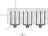
- Fig. 1 illustrates an arrangement pattern of a common electrode 1 and pixel electrodes 2, where the pattern of the common electrode 1 is like a comb, and since the widths of body connection sections 1a of the common electrode 1 are larger, there are lower resistances of the body connection sections 1a, and high resistances of teeth 1b of the comb, so that there is a non-uniform resistance of the common electrode 1 as a whole, thus degrading a display effect of a display device as a whole.
- the embodiments of this disclosure provide an array substrate and a display device so as to address the problem in the array substrate in the related art that the resistances of the common electrodes are not uniform in the arrangement pattern of the common electrodes and the pixel electrodes, thus degrading a display effect of the display device as a whole.
- an arrangement pattern of common electrodes is changed in an array substrate according to some embodiments of this disclosure in such a way that body connection sections of two adjacent sub-common electrodes in each common electrode are arranged on two opposite sides, that is, two adjacent body connection sections with lower resistances in each common electrode are arranged on two sides, so that the uniformity of the resistance of the common electrode can be improved to thereby improve a display effect of a display device as a whole.
- a particular structure of the array substrate will be described below in details.
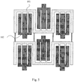
- Fig. 2 illustrates a schematic structural diagram of an array substrate according to some embodiments of this disclosure in a top view; and for the sake of a convenient description, only 3 by 2 sub-pixel elements are illustrated in the embodiment of this disclosure, and Fig. 2 is only a schematic diagram, but a real fabrication process will not be only limited to3 by 2 sub-pixel elements, and the sub-pixel elements can alternatively be arranged in other different patterns, although a common rectangular arrangement pattern is illustrated in the embodiment of this disclosure only by way of an example.
- the array substrate according to the embodiment of this disclosure can be structured differently, and Fig. 2 illustrates only one of feasible structures of the array substrate only for the sake of a convenient description, but this disclosure will not be limited thereto. A number of array substrates in other structures will be further described in further embodiments of this disclosure hereinafter.
- an array substrate includes: a plurality of sub-pixel elements P arranged in an array; there is a common electrode 101 for each row of sub-pixel elements P.
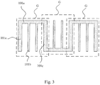
- Fig. 3 illustrates a schematic structural diagram of a separate common electrode 101 corresponding to Fig. 2 according to some embodiments of this disclosure, that is, Fig. 3 illustrates a schematic structural diagram of a common electrode 101 according to some embodiments of this disclosure in a top view; and each common electrode 101 includes a plurality of sub-common electrodes G, each of which corresponds to one of the sub-pixel elements P.
- the sub-common electrode G includes a body connection section 101a, a plurality of comb teeth 101b connected with the body connection section 101a, and a shielding section 101c connected with the body connection section 101a, where the first comb teeth 101b and the shielding section 101c are located on the same side of the body connection section 101a, and the shielding section 101c is located on the outermost side of the first comb teeth 101b.
- the body connection sections 101a of two adjacent sub-common electrodes G in the common electrode 101 are located on two opposite sides.
- both the first comb teeth 101b and the shielding section 101c can be arranged perpendicular to the body connection section 101a; or of course, they can alternatively be arranged in other structures, and the body connection section 101a, the first comb teeth 101b, and the shielding section 101c may not be arranged in a regular rectangular structure, but may be arranged in other structures as needed.
- the drawing in the embodiment of this disclosure is only one of feasible schematic structural diagrams, but not intended to limit this disclosure thereto.
- the body connection sections 101a of two adjacent sub-common electrodes G in each common electrode 101 are located on two opposite sides, that is, the body connection sections 101a of the first sub-common electrode G and the second sub-common electrode G from the left to the right are arranged on two opposite sides, and the body connection sections 101a of the second sub-common electrode G and the third sub-common electrode G from the left to the right are also arranged on two opposite sides; and the other sub-common electrodes G are arranged alternately in this way, as illustrated in Fig. 2 and Fig. 3 .
- the body connection section 101a of each sub-common electrode G generally has a larger width and a lower resistance, so the body connection sections 101a of two adjacent sub-common electrodes G in each common electrode 101 are located on two opposite sides in the embodiment of this disclosure, so that adjacent body connection sections 101a with lower resistances in each common electrode 101 can be arranged on two sides in a disperse manner to thereby improve the uniformity of the resistance of the common electrode 101 so as to improve a display effect of a display device as a whole.
- two adjacent sub-common electrodes G in each common electrode 101 can share one shielding section 101c so that the two sub-common electrodes G are connected with each other through the shielding section 101c, as illustrated in Fig. 2 and Fig. 3 .
- each sub-pixel element P includes a pixel electrode 102 including a protruding connection section 102a and an electrode section 102b, and in each sub-pixel element P, the protruding connection section 102a of the pixel electrode 102, and the body connection section 101a of the sub-common electrode G can be located on two opposite sides to thereby save a layout space, where the protruding connection section 102a is a channel over which a display signal is applied to the pixel electrode 102, and the electrode section 102b of the pixel electrode 102 cooperates with the first comb tooth 101b of the sub-common electrode G to form an electric field for controlling liquid crystals to be deflected.
- a particular shape of the electrode section 102b can be set as needed, and for example, the electrode section 102b of the pixel electrode 102 can be set in a plate structure or in a structure including branches. This will be described below with reference to the drawings, so a repeated description thereof will be omitted here.
- the array substrate may further include other layers or structures, thin film transistors, data lines, gate lines, etc., in addition to the pixel electrodes 102 and the common electrodes 101 above. All of these structures can be arranged as needed, although the embodiment of this disclosure will not be limited thereto.
- the array substrate can further include data lines 103 and gate lines 104, where the data lines 103 generally extend in the same direction as the shielding sections 101c of the common electrodes G, there are overlapping areas between orthographic projections of the data lines 103 in the direction perpendicular to the array substrate, and orthographic projections of the shielding sections 101c of the common electrodes G in the direction perpendicular to the array substrate, and the gate lines 104 generally extend in the direction intersecting with the data lines 103.
- a thin film transistor is generally arranged in each sub-pixel element P, where the thin film transistor has a source 105a connected with the data line 103, a drain 105b connected with the protruding connection section 102a of the pixel electrode 102, and a gate 105c connected with the gate line 104.
- the data line 103 and the shielding section 101c are generally arranged in the column direction (i.e., in the direction of the y axis), and particularly can be arranged in the form of a straight line as illustrated in Fig. 2 .
- the shielding section 101c is primarily configured to shield a data signal applied to the data line 103 from affecting the pixel electrode 102, the shielding section 101c is actually also a part of the sub-common electrode G, so a part of the data line 103 shall be shielded by the shielding section 101c of the sub-common electrode G.
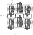
- the data lines 103 can be arranged as bent lines arranged in the extension direction of the shielding sections 101c of the sub-common electrodes G, and particularly as illustrated in Fig. 4 , when the sub-common electrodes G are arranged as bent structures, the corresponding data lines 103 can also be arranged as bent lines bent at the same angle as the shielding sections 101c; and both the common electrodes 101 and the pixel electrodes 102 in Fig. 4 are also bent structures, and correspondingly the data lines 103 are also arranged as bent lines, where Fig. 4 only illustrates the data lines 103 by way of an example, but the real shape, widths, etc., of the data lines will not be limited thereto in a real fabrication process.
- the gate lines 104 are generally arranged in the row direction (i.e., in the direction of the x axis), and particularly can be arranged in the form of a straight line or a bent line, i.e., in the structure as illustrated in Fig. 2 , so that the sub-pixel elements P are arranged more densely to thereby save a layout space.
- the protruding connection sections 102a of the respective pixel electrodes 102 are arranged alternately in parallel in the sub-pixel elements P connected with the same gate line 104.
- the body connection sections 101a of two adjacent sub-common electrodes G in each common electrode 101 are located on two opposite sides, and the body connection section 101a of each sub-common electrode G, and the protruding connection section 102a of the pixel electrode 102 are located on two opposite sides, so as illustrated in Fig. 2 , the protruding connection sections 102a of adjacent pixel electrodes 102 are actually also located on two opposite sides, so that the pixel electrodes 102 connected with the same gate line 104 generally also belong to two rows of sub-pixel elements P, and optionally, two adjacent sub-pixel elements P connected with each gate line 104 belong respectively to different rows.
- the protruding connection sections 102a of the pixel electrodes 102 connected with the same gate line 104 can be arranged alternately in parallel so that the protruding connection sections 102a of the pixel electrodes 102 connected with the same gate line 104 and located in two adjacent columns of sub-pixel elements P substantially lie on the same straight line, and the protruding connection sections 102a of the respective pixel electrodes 102 are arranged alternately in parallel, thus enabling the sub-pixel elements P to be arranged more densely, i.e., the structure as illustrated in Fig. 2 .
- the pixel electrodes 102 and the common electrodes 101 there are a number of different structures and fabrication processes of the pixel electrodes 102 and the common electrodes 101, and for example, they can be fabricated together at the same layer, or can be arranged separately at different layer. Several particular structures thereof will be described below respectively.
- the pixel electrodes 102 and the common electrodes 101 can be arranged at the same layer, and orthographic projections of the pixel electrodes 102 in the direction perpendicular to the array substrate do not overlap with the orthographic projections of the common electrodes 101 in the direction perpendicular to the array substrate.
- the pixel electrodes 102 and the common electrodes 101 are generally made of a transparent conductive material, metal, or another material. Since the pixel electrodes 102 and the common electrodes 101 are formed at the same layer, and each sub-pixel element P corresponds to one pixel electrode 102, and a part of the common electrode 101 (e.g., one sub-common electrode G in Fig. 2 ), and the sub-common electrodes G in each common electrode 101 are comblike interdigital electrodes, the pixel electrode 102 can also be comblike arranged as an interdigital electrode.
- the electrode section 102b of the pixel electrode 102 generally includes a plurality of second comb teeth 102b1 connected with the protruding connection section 102a, where both the second comb teeth 102b1, and the first comb teeth 101b of the common electrode G are tooth branches, and can be arranged to be interleaved into each other, that is, the second comb teeth 102b1 of the pixel electrodes 102 can be interlaced into the first comb teeth 101b of the common electrode G.
- the pixel electrodes 102 and the common electrodes 101 can alternatively be arranged at different layers, and at this time, the electrode section 102b of the pixel electrode 102 can be a plate electrode.
- the pixel electrodes 102 and the common electrodes 101 are not formed at the same layer, they are generally made of indium tin oxide (ITO), metal, or another material. At this time, since the pixel electrode 102 is fabricated separately, it can be arranged as a plate electrode.
- ITO indium tin oxide
- pixel electrodes 102 and the common electrodes 101 can be structures including straight edges, or can be structures including bent edges, so that an image can be displayed in a multi-domain mode.
- the pixel electrodes 102 and the common electrodes 101 can be arranged as straight structures, that is, the electrode sections 102b of the pixel electrodes 102 are structures including straight edges, and the first comb teeth 101a of the common electrodes 101 are straight; and particularly when the pixel electrodes 102 and the common electrodes 101 are arranged at the same layer, they can formed in the structure as illustrated in Fig. 2 ; and when the pixel electrodes 102 and the common electrodes 101 are arranged at different layers, they can formed in the structure as illustrated in Fig. 5 .
- the pixel electrodes 102 and the common electrodes 101 can alternatively be arranged as bent structures, that is, the electrode sections 102b of the pixel electrodes 102 are structures including bent edges, and the first comb teeth 101a of the common electrodes 101 are bent; and the bending angle of the folded lines of the electrode sections 102b is the same as the bending angle of the folded lines of the first comb teeth 101b, so that an image can be displayed at a larger angle of view in a multi-domain mode.
- the first comb teeth 101b and the shielding sections 101c of the common electrodes 101 shall be bent at a specific angle at their centers, and correspondingly the plate pixel electrodes 102 shall also be modified in shape at the centers of the electrode sections 102b.
- the particular bending angle can be set as needed, and for example, the bending angle can be set between 160 degrees and 180 degrees, between 10 degrees and 20 degrees, etc.
- the pixel electrodes 102 and the common electrodes 101 are arranged at the same layer, they can be formed in the structure as illustrated in Fig. 4 ; and when the pixel electrodes 102 and the common electrodes 101 are arranged at different layers, they can be formed in the structure as illustrated in Fig. 6 .
- a plurality of common electrodes 101 can be connected together, optionally in an array substrate with a larger size.
- the sub-common electrodes G in two adjacent common electrodes 101 can be electrically connected through a connection line, and for example, the shielding sections 101c of two facing sub-common electrodes G can be connected together.
- the respective common electrodes 101 can be formed directly along with the connection line.
- the pixel electrodes 102 in Fig. 5 and Fig. 6 are illustrated transparently only for their clarity, but neither a real fabrication process nor this disclosure will be limited thereto.
- some embodiments of this disclosure further provide a display device including the array substrate according to any one of the embodiments above of this disclosure.
- a display device including the array substrate according to any one of the embodiments above of this disclosure.
- each common electrode includes a plurality of sub-common electrodes, and each sub-common electrode generally includes a body connection section with a larger width and a lower resistance, and first comb teeth with a smaller width and a higher resistance; and in the embodiments of this disclosure, the body connection sections of two adjacent sub-common electrodes in each common electrode are arranged in two opposite directions, and correspondingly adjacent body connection sections with a lower resistance in the respective common electrodes are arranged separately on two sides, thus improving the uniformity of the resistance of the common electrode so as to improve a display effect of the display device as a whole.
Landscapes
- Physics & Mathematics (AREA)
- Nonlinear Science (AREA)
- Mathematical Physics (AREA)
- Chemical & Material Sciences (AREA)
- Crystallography & Structural Chemistry (AREA)
- General Physics & Mathematics (AREA)
- Optics & Photonics (AREA)
- Engineering & Computer Science (AREA)
- Microelectronics & Electronic Packaging (AREA)
- Liquid Crystal (AREA)
- Geometry (AREA)
- Devices For Indicating Variable Information By Combining Individual Elements (AREA)
Applications Claiming Priority (2)
| Application Number | Priority Date | Filing Date | Title |
|---|---|---|---|
| CN201721381384.1U CN207396936U (zh) | 2017-10-24 | 2017-10-24 | 一种阵列基板及显示装置 |
| PCT/CN2018/100076 WO2019080596A1 (zh) | 2017-10-24 | 2018-08-10 | 阵列基板及显示装置 |
Publications (3)
| Publication Number | Publication Date |
|---|---|
| EP3702834A1 true EP3702834A1 (de) | 2020-09-02 |
| EP3702834A4 EP3702834A4 (de) | 2021-08-04 |
| EP3702834B1 EP3702834B1 (de) | 2025-12-17 |
Family
ID=62330159
Family Applications (1)
| Application Number | Title | Priority Date | Filing Date |
|---|---|---|---|
| EP18869964.9A Active EP3702834B1 (de) | 2017-10-24 | 2018-08-10 | Arraysubstrat und anzeigevorrichtung |
Country Status (4)
| Country | Link |
|---|---|
| US (1) | US11527556B2 (de) |
| EP (1) | EP3702834B1 (de) |
| CN (1) | CN207396936U (de) |
| WO (1) | WO2019080596A1 (de) |
Cited By (2)
| Publication number | Priority date | Publication date | Assignee | Title |
|---|---|---|---|---|
| US11215890B2 (en) * | 2018-11-19 | 2022-01-04 | Chengdu Boe Optoelectronics Technology Co., Ltd. | Array substrate, display panel and display device |
| CN114019731A (zh) * | 2021-04-21 | 2022-02-08 | 友达光电股份有限公司 | 显示面板 |
Families Citing this family (5)
| Publication number | Priority date | Publication date | Assignee | Title |
|---|---|---|---|---|
| CN207396936U (zh) | 2017-10-24 | 2018-05-22 | 京东方科技集团股份有限公司 | 一种阵列基板及显示装置 |
| CN115693161B (zh) * | 2021-07-30 | 2026-04-07 | 北京京东方技术开发有限公司 | 液晶天线及通信设备 |
| WO2023039887A1 (zh) * | 2021-09-18 | 2023-03-23 | 京东方科技集团股份有限公司 | 显示基板及显示装置 |
| CN114924437B (zh) * | 2022-05-20 | 2024-01-12 | 北京京东方技术开发有限公司 | 阵列基板及其制备方法、显示装置 |
| US12461405B2 (en) | 2022-11-23 | 2025-11-04 | Hefei Boe Optoelectronics Technology Co., Ltd. | Display device |
Family Cites Families (12)
| Publication number | Priority date | Publication date | Assignee | Title |
|---|---|---|---|---|
| KR100490019B1 (ko) * | 2000-06-20 | 2005-05-17 | 인터내셔널 비지네스 머신즈 코포레이션 | 다중 도메인을 갖는 넓은 시야각의 액정 디스플레이와 넓은 시야각의 ips 모드 액정 디스플레이 및 그 제공 방법 |
| KR100918651B1 (ko) * | 2002-10-30 | 2009-09-22 | 엘지디스플레이 주식회사 | 횡전계형 액정 표시 장치 및 그 제조 방법 |
| KR101408252B1 (ko) * | 2007-06-22 | 2014-06-17 | 엘지디스플레이 주식회사 | 액정표시장치 및 그 제조방법 |
| JP5266578B2 (ja) * | 2008-07-22 | 2013-08-21 | Nltテクノロジー株式会社 | 横電界方式の液晶表示装置 |
| KR101749757B1 (ko) * | 2010-11-03 | 2017-07-04 | 엘지디스플레이 주식회사 | 고 투과 수평 전계형 액정표시장치 및 그 제조 방법 |
| CN103163701B (zh) * | 2011-12-16 | 2015-09-30 | 上海中航光电子有限公司 | 网状公共电极结构液晶显示器件及其制造方法 |
| CN202487576U (zh) * | 2012-02-09 | 2012-10-10 | 京东方科技集团股份有限公司 | 阵列基板和双视场显示装置 |
| CN103901684B (zh) | 2012-12-28 | 2018-02-09 | 上海中航光电子有限公司 | 一种ips模式的液晶显示器 |
| CN105278194B (zh) * | 2015-11-24 | 2019-06-07 | 京东方科技集团股份有限公司 | 一种阵列基板及其制备方法、显示装置及其控制方法 |
| KR102439350B1 (ko) * | 2015-12-31 | 2022-09-02 | 엘지디스플레이 주식회사 | 터치스크린 내장형 표시장치 및 그 제조방법 |
| JP2017173624A (ja) * | 2016-03-24 | 2017-09-28 | パナソニック液晶ディスプレイ株式会社 | 液晶表示装置 |
| CN207396936U (zh) * | 2017-10-24 | 2018-05-22 | 京东方科技集团股份有限公司 | 一种阵列基板及显示装置 |
-
2017
- 2017-10-24 CN CN201721381384.1U patent/CN207396936U/zh active Active
-
2018
- 2018-08-10 US US16/329,796 patent/US11527556B2/en active Active
- 2018-08-10 EP EP18869964.9A patent/EP3702834B1/de active Active
- 2018-08-10 WO PCT/CN2018/100076 patent/WO2019080596A1/zh not_active Ceased
Cited By (3)
| Publication number | Priority date | Publication date | Assignee | Title |
|---|---|---|---|---|
| US11215890B2 (en) * | 2018-11-19 | 2022-01-04 | Chengdu Boe Optoelectronics Technology Co., Ltd. | Array substrate, display panel and display device |
| CN114019731A (zh) * | 2021-04-21 | 2022-02-08 | 友达光电股份有限公司 | 显示面板 |
| CN114019731B (zh) * | 2021-04-21 | 2023-07-04 | 友达光电股份有限公司 | 显示面板 |
Also Published As
| Publication number | Publication date |
|---|---|
| US20210366947A1 (en) | 2021-11-25 |
| EP3702834B1 (de) | 2025-12-17 |
| EP3702834A4 (de) | 2021-08-04 |
| WO2019080596A1 (zh) | 2019-05-02 |
| US11527556B2 (en) | 2022-12-13 |
| CN207396936U (zh) | 2018-05-22 |
Similar Documents
| Publication | Publication Date | Title |
|---|---|---|
| US11527556B2 (en) | Array substrate and display device | |
| EP3872561B1 (de) | Array-substrat | |
| US10325933B2 (en) | Array substrate and manufacturing method thereof, display device | |
| US10013086B2 (en) | In cell touch panel and method for driving the same, and display device | |
| JP6456073B2 (ja) | 液晶表示装置 | |
| CN104865737B (zh) | 一种显示面板、其驱动方法及显示装置 | |
| US9335591B2 (en) | Array substrate, display panel and display device | |
| US10203569B2 (en) | Array substrate and display panel | |
| EP3677960A1 (de) | Anzeigesubstrat, anzeigetafel und anzeigevorrichtung | |
| CN102902119B (zh) | 液晶显示面板 | |
| US10559270B2 (en) | Array substrate and display panel | |
| CN107219667B (zh) | 曲面显示面板和显示装置 | |
| KR20150073752A (ko) | 액정표시장치 | |
| CN105629610A (zh) | 显示基板、显示面板、显示装置 | |
| CN102262322B (zh) | 液晶显示装置与液晶显示装置基板 | |
| CN110531558B (zh) | 阵列基板、液晶显示面板及显示装置 | |
| WO2019200964A1 (zh) | 显示基板和显示装置 | |
| CN108490705B (zh) | 阵列基板、液晶显示面板与显示装置 | |
| KR20140006281A (ko) | 표시 장치 | |
| CN110531557B (zh) | 阵列基板、液晶显示面板及显示装置 | |
| CN204314581U (zh) | 一种阵列基板、显示面板和显示装置 | |
| KR102537280B1 (ko) | 표시 기판 및 이를 포함하는 액정 표시 장치 | |
| KR20070059558A (ko) | 액정 표시 장치 | |
| EP3607398B1 (de) | Arraysubstrat, flüssigkristallanzeigetafel und flüssigkristallanzeigevorrichtung | |
| CN120129887A (zh) | 触控显示基板及触控显示装置 |
Legal Events
| Date | Code | Title | Description |
|---|---|---|---|
| STAA | Information on the status of an ep patent application or granted ep patent |
Free format text: STATUS: THE INTERNATIONAL PUBLICATION HAS BEEN MADE |
|
| PUAI | Public reference made under article 153(3) epc to a published international application that has entered the european phase |
Free format text: ORIGINAL CODE: 0009012 |
|
| STAA | Information on the status of an ep patent application or granted ep patent |
Free format text: STATUS: REQUEST FOR EXAMINATION WAS MADE |
|
| 17P | Request for examination filed |
Effective date: 20190522 |
|
| AK | Designated contracting states |
Kind code of ref document: A1 Designated state(s): AL AT BE BG CH CY CZ DE DK EE ES FI FR GB GR HR HU IE IS IT LI LT LU LV MC MK MT NL NO PL PT RO RS SE SI SK SM TR |
|
| AX | Request for extension of the european patent |
Extension state: BA ME |
|
| DAV | Request for validation of the european patent (deleted) | ||
| DAX | Request for extension of the european patent (deleted) | ||
| A4 | Supplementary search report drawn up and despatched |
Effective date: 20210705 |
|
| RIC1 | Information provided on ipc code assigned before grant |
Ipc: G02F 1/1343 20060101AFI20210629BHEP Ipc: G02F 1/1362 20060101ALI20210629BHEP |
|
| STAA | Information on the status of an ep patent application or granted ep patent |
Free format text: STATUS: EXAMINATION IS IN PROGRESS |
|
| 17Q | First examination report despatched |
Effective date: 20230201 |
|
| P01 | Opt-out of the competence of the unified patent court (upc) registered |
Effective date: 20230527 |
|
| GRAP | Despatch of communication of intention to grant a patent |
Free format text: ORIGINAL CODE: EPIDOSNIGR1 |
|
| STAA | Information on the status of an ep patent application or granted ep patent |
Free format text: STATUS: GRANT OF PATENT IS INTENDED |
|
| INTG | Intention to grant announced |
Effective date: 20250808 |
|
| GRAS | Grant fee paid |
Free format text: ORIGINAL CODE: EPIDOSNIGR3 |
|
| GRAA | (expected) grant |
Free format text: ORIGINAL CODE: 0009210 |
|
| STAA | Information on the status of an ep patent application or granted ep patent |
Free format text: STATUS: THE PATENT HAS BEEN GRANTED |
|
| AK | Designated contracting states |
Kind code of ref document: B1 Designated state(s): AL AT BE BG CH CY CZ DE DK EE ES FI FR GB GR HR HU IE IS IT LI LT LU LV MC MK MT NL NO PL PT RO RS SE SI SK SM TR |
|
| REG | Reference to a national code |
Ref country code: CH Ref legal event code: F10 Free format text: ST27 STATUS EVENT CODE: U-0-0-F10-F00 (AS PROVIDED BY THE NATIONAL OFFICE) Effective date: 20251217 Ref country code: GB Ref legal event code: FG4D |
|
| REG | Reference to a national code |
Ref country code: DE Ref legal event code: R096 Ref document number: 602018088020 Country of ref document: DE |
|
| REG | Reference to a national code |
Ref country code: LT Ref legal event code: MG9D |
|
| PG25 | Lapsed in a contracting state [announced via postgrant information from national office to epo] |
Ref country code: NO Free format text: LAPSE BECAUSE OF FAILURE TO SUBMIT A TRANSLATION OF THE DESCRIPTION OR TO PAY THE FEE WITHIN THE PRESCRIBED TIME-LIMIT Effective date: 20260317 |
|
| PG25 | Lapsed in a contracting state [announced via postgrant information from national office to epo] |
Ref country code: FI Free format text: LAPSE BECAUSE OF FAILURE TO SUBMIT A TRANSLATION OF THE DESCRIPTION OR TO PAY THE FEE WITHIN THE PRESCRIBED TIME-LIMIT Effective date: 20251217 Ref country code: HR Free format text: LAPSE BECAUSE OF FAILURE TO SUBMIT A TRANSLATION OF THE DESCRIPTION OR TO PAY THE FEE WITHIN THE PRESCRIBED TIME-LIMIT Effective date: 20251217 |
|
| PG25 | Lapsed in a contracting state [announced via postgrant information from national office to epo] |
Ref country code: RS Free format text: LAPSE BECAUSE OF FAILURE TO SUBMIT A TRANSLATION OF THE DESCRIPTION OR TO PAY THE FEE WITHIN THE PRESCRIBED TIME-LIMIT Effective date: 20260317 |