EP3607398B1 - Arraysubstrat, flüssigkristallanzeigetafel und flüssigkristallanzeigevorrichtung - Google Patents
Arraysubstrat, flüssigkristallanzeigetafel und flüssigkristallanzeigevorrichtung Download PDFInfo
- Publication number
- EP3607398B1 EP3607398B1 EP17903368.3A EP17903368A EP3607398B1 EP 3607398 B1 EP3607398 B1 EP 3607398B1 EP 17903368 A EP17903368 A EP 17903368A EP 3607398 B1 EP3607398 B1 EP 3607398B1
- Authority
- EP
- European Patent Office
- Prior art keywords
- electrode layer
- liquid crystal
- crystal display
- display panel
- teeth
- Prior art date
- Legal status (The legal status is an assumption and is not a legal conclusion. Google has not performed a legal analysis and makes no representation as to the accuracy of the status listed.)
- Active
Links
Images


Classifications
-
- G—PHYSICS
- G02—OPTICS
- G02F—OPTICAL DEVICES OR ARRANGEMENTS FOR THE CONTROL OF LIGHT BY MODIFICATION OF THE OPTICAL PROPERTIES OF THE MEDIA OF THE ELEMENTS INVOLVED THEREIN; NON-LINEAR OPTICS; FREQUENCY-CHANGING OF LIGHT; OPTICAL LOGIC ELEMENTS; OPTICAL ANALOGUE/DIGITAL CONVERTERS
- G02F1/00—Devices or arrangements for the control of the intensity, colour, phase, polarisation or direction of light arriving from an independent light source, e.g. switching, gating or modulating; Non-linear optics
- G02F1/01—Devices or arrangements for the control of the intensity, colour, phase, polarisation or direction of light arriving from an independent light source, e.g. switching, gating or modulating; Non-linear optics for the control of the intensity, phase, polarisation or colour
- G02F1/13—Devices or arrangements for the control of the intensity, colour, phase, polarisation or direction of light arriving from an independent light source, e.g. switching, gating or modulating; Non-linear optics for the control of the intensity, phase, polarisation or colour based on liquid crystals, e.g. single liquid crystal display cells
- G02F1/133—Constructional arrangements; Operation of liquid crystal cells; Circuit arrangements
- G02F1/1333—Constructional arrangements; Manufacturing methods
- G02F1/1343—Electrodes
- G02F1/134309—Electrodes characterised by their geometrical arrangement
- G02F1/134372—Electrodes characterised by their geometrical arrangement for fringe field switching [FFS] where the common electrode is not patterned
-
- G—PHYSICS
- G02—OPTICS
- G02F—OPTICAL DEVICES OR ARRANGEMENTS FOR THE CONTROL OF LIGHT BY MODIFICATION OF THE OPTICAL PROPERTIES OF THE MEDIA OF THE ELEMENTS INVOLVED THEREIN; NON-LINEAR OPTICS; FREQUENCY-CHANGING OF LIGHT; OPTICAL LOGIC ELEMENTS; OPTICAL ANALOGUE/DIGITAL CONVERTERS
- G02F2201/00—Constructional arrangements not provided for in groups G02F1/00 - G02F7/00
- G02F2201/12—Constructional arrangements not provided for in groups G02F1/00 - G02F7/00 electrode
- G02F2201/121—Constructional arrangements not provided for in groups G02F1/00 - G02F7/00 electrode common or background
-
- G—PHYSICS
- G02—OPTICS
- G02F—OPTICAL DEVICES OR ARRANGEMENTS FOR THE CONTROL OF LIGHT BY MODIFICATION OF THE OPTICAL PROPERTIES OF THE MEDIA OF THE ELEMENTS INVOLVED THEREIN; NON-LINEAR OPTICS; FREQUENCY-CHANGING OF LIGHT; OPTICAL LOGIC ELEMENTS; OPTICAL ANALOGUE/DIGITAL CONVERTERS
- G02F2201/00—Constructional arrangements not provided for in groups G02F1/00 - G02F7/00
- G02F2201/12—Constructional arrangements not provided for in groups G02F1/00 - G02F7/00 electrode
- G02F2201/123—Constructional arrangements not provided for in groups G02F1/00 - G02F7/00 electrode pixel
Definitions
- the present invention relates to display technology, more particularly, to an array substrate, a liquid crystal display panel and a liquid crystal display apparatus.
- a fringe field driven liquid crystal display panel the liquid crystal layer is driven by a fringe electric field.
- fringe field driven liquid crystal display panel include an advanced super-dimensional switching (ADS) liquid crystal display panel.
- ADS liquid crystal display panel a multi-dimensional electrical field is formed by an electric field generated by edges of slit electrodes in a same plane, and an electric field generated by a slit electrode layer and a plate electrode layer.
- the liquid crystal molecules between the slit electrodes and above the slit electrodes are rotated by the above-mentioned electrode fields.
- the operation efficiency and the light transmittance efficiency of the liquid crystal display panel are greatly improved in the ADS liquid crystal display panel.
- US 2008/068539 A1 discloses a liquid crystal display panel including an array substrate.
- the array substrate includes a plurality of scan lines provided in parallel with one another, and a plurality of signal lines provided in a direction orthogonal to the scan lines.
- First electrodes are each provided in a space delimited by the scan lines and the signal lines, second electrodes are provided corresponding to the first electrodes with an insulator therebetween, and a plurality of slits are provided to each of the second electrodes in parallel with one another in a direction crossing the signal lines.
- Each slit has a closed end on one side, and an open end on the other.
- CN 105 676 550 A discloses an array substrate comprising a slit electrode.
- the slit electrode comprises a plurality of slits; and one end of each of the slits is opened.
- the plurality of electrode strips are connected electrically.
- two adjacent electrode strips are parallel with each other.
- a slit is formed between two adjacent electrode strips, in which openings of slits between one electrode strip and two electrode strips adjacent to this electrode strip are disposed on different sides of the slit electrode.
- US 2012/249496 A1 discloses a pixel array of a fringe field switching liquid crystal display panel including a plurality of gate lines, a plurality of data lines, a plurality of pixel electrodes, and a plurality of common lines.
- the plurality of pixel electrodes respectively disposed in each of the sub-pixel regions.
- Each of the pixel electrodes includes a plurality of stripe structures for driving the fringe field switching liquid crystal display panel.
- the present invention provides an array substrate according to claim 1.
- the first electrode layer is a plate electrode layer extending substantially throughout one of the plurality of subpixel areas.
- each of the plurality of branches extends substantially throughout the one dimension of the second electrode layer.
- the first end and the second end are in peripheral regions of the second electrode layer.
- the plurality of branches extend substantially along a longitudinal direction of the subpixel area.
- the first electrode layer is a common electrode layer
- the second electrode layer is a pixel electrode layer
- the second electrode layer is a common electrode layer
- the first electrode layer is a pixel electrode layer
- the present invention provides a liquid crystal display panel comprising the array substrate described herein, a counter substrate facing the array substrate, and a liquid crystal layer between the array substrate and the counter substrate.
- the liquid crystal display panel is a fringe field driven liquid crystal display panel, in which liquid crystal molecules in the liquid crystal layer is driven by a fringe electric field.
- the present invention provides a liquid crystal display apparatus comprising a liquid crystal display panel described herein.
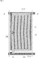
- FIG. 1 is a schematic diagram illustrating the structure of a conventional liquid crystal display panel.
- FIG. 2 is a cross-sectional view along A-A' line of the liquid crystal display panel in FIG. 1 .
- the conventional liquid crystal display panel includes an array substrate 1, a counter substrate 2 facing the array substrate 1, and a liquid crystal layer 3 between the array substrate 1 and the counter substrate 2.
- the liquid crystal display panel includes a first electrode layer 11, a second electrode layer 12, and an insulating layer 13 between the first electrode layer 11 and the second electrode layer 12.
- the second electrode layer 12 may be, for example, a pixel electrode layer.
- the pixel electrode layer includes a plurality of branches 12B spaced apart by a plurality of slits S.
- the plurality of branches 12B are connected together by a first bar 12-1 at the bottom of the second electrode layer 12 and a second bar 12-2 at the top of the second electrode layer 12.
- Each of the plurality of slits S has a first end and a second end, both of which are closed ends.
- the first bar 12-1 and the second bar 12-2 close each of the plurality of slits S at its first end and the second end.
- the first electrode layer 11 extends to the edges of the subpixel area. Referring to FIG. 1 , a projection of the first electrode layer 11 on a base substrate 10 overlaps with that of the first bar 12-1 of the second electrode layer 12 throughout the width of the first electrode layer 11 along the edge of the subpixel area.
- a large storage capacitance forms between the first electrode layer 11 and the second electrode layer 12.
- the first electrode layer 11 and the second electrode layer 12 are made of indium tin oxide or other similar metal oxide or transparent conductive materials.
- light has to pass through two electrode layers, e.g., first passing through the first electrode layer 11, then passing through the first bar 12-1 or the second bar 12-2.
- light transmittance in the regions corresponding to the first bar 12-1 and the second bar 12-2 is reduced, e.g., by 20%, forming dark areas along the edges of the subpixel area.
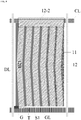
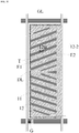
- FIG. 3 is a schematic diagram illustrating the structure of a liquid crystal display panel according to the present invention.
- FIG. 4 is a cross-sectional view along B-B' line of the liquid crystal display panel in FIG. 3 .
- the liquid crystal display panel includes an array substrate 1, a counter substrate 2 facing the array substrate 1, and a liquid crystal layer 3 between the array substrate 1 and the counter substrate 2.
- the liquid crystal display panel includes a plurality of subpixels. In each subpixel, the liquid crystal display panel includes a first electrode layer 11, a second electrode layer 12, and an insulating layer 13 between the first electrode layer 11 and the second electrode layer 12.
- the first electrode layer 11 and the second electrode layer 12 are configured to form a fringe field for driving liquid crystal molecules in the liquid crystal layer 3.
- the liquid crystal display panel further includes a plurality of gate lines GL and a plurality of data lines DL crossing over each other thereby defining a plurality of subpixels.
- Each subpixel further includes a switching thin film transistor having a gate electrode G for driving image display in the subpixel.
- the second electrode layer 12 is a pixel electrode layer (as shown in FIG. 3 )
- the second electrode layer 12 is connected to a drain electrode of the switching thin film transistor, and one of the plurality of data lines DL is connected to a source electrode of the switching thin film transistor.
- the second electrode layer 12 is a common electrode layer
- the first electrode layer 11 is a pixel electrode layer
- the first electrode layer 11 is connected to the drain electrode of the switching thin film transistor.
- the first electrode layer 11 (e.g., a common electrode layer) is a plate electrode layer that extends substantially throughout the subpixel, e.g., extending to a first edge of the subpixel (e.g., proximal to the B-B' line in FIG. 3 ).
- the second electrode layer 12 includes a plurality of branches 12B, each of which extends substantially along a longitudinal direction of the subpixel.
- the plurality of branches 12B extend along a direction substantially parallel to the plurality of data lines DL.
- the plurality of branches 12B extend along a direction substantially parallel to the plurality of gate lines GL.
- the plurality of branches 12B are spaced apart by a plurality of slits (e.g., a first slit S1 in FIG. 3 ).
- each of the plurality of branches 12B corresponds to one of the plurality of teeth T, e.g., each of the plurality of teeth T includes only one of the plurality of branches 12B. Adjacent teeth of the plurality of teeth T are spaced apart by a first slit S1. Thus, in the embodiment depicted in FIG. 3 , adjacent branches of the plurality of branches 12B are spaced apart by a first slit S1.
- the first slit S1 is open at a first end E1 (e.g., the end proximal to a first signal line along a first edge of the subpixel), and closed at a second end E2 (e.g., the end proximal to a second signal line along a second edge of the subpixel, the second edge opposite to the first edge).
- the first end E1 is opposite to the second end E2.
- the first slit S1 extends along a direction substantially parallel to the adjacent teeth (or adjacent branches 12B in an embodiment depicted in FIG.
- first end E1 of the first slit S1 proximal to a first end of one of the plurality of branches 12B and distal to a second end of the one of the plurality of branches 12B opposite to the first end of the one of the plurality of branches 12B; and the second end E2 of the first slit S1 proximal to the second end of one of the plurality of branches 12B and distal to the first end of the one of the plurality of branches 12B.
- the first slit S1 extends substantially throughout one dimension of the second electrode layer 12, e.g., throughout the longitudinal dimension of the second electrode layer 12. Adjacent teeth are separated from each other at the first end E1 and connected to each other at the second end E2. In the embodiments depicted in FIG. 3 , adjacent branches of the plurality of branches 12B are separated from each other at the first end E1 and connected to each other at the second end E2.
- the second electrode layer 12 is a comb-shaped electrode layer having a plurality of teeth T and a bar (e.g., a first bar 12-1 as shown in FIG. 3 ) connecting the adjacent teeth of the plurality of teeth T at the second end E2.
- the liquid crystal display panel as shown in FIG. 3 only has one bar along only one edge of the subpixel, e.g., lacks a second bar along an opposite edge of the subpixel. Comparing the cross-sections illustrated in FIG. 2 and FIG. 4 , the present design greatly reduces the overlapping area between the first electrode layer 11 and the second electrode layer 12.
- the present liquid crystal display panel includes multiple slits along the edge of the subpixel, in these areas, light need not pass through two electrode layers.
- light transmittance along the edges of the subpixels is significantly improved, obviating the issue of dark areas along the edges of the subpixels.
- each of the plurality of branches 12B extends substantially throughout one dimension (e.g., the longitudinal dimension) of the second electrode layer 12. Any structure connecting the adjacent teeth or adjacent branches is disposed in peripheral regions of the second electrode layer 12. The first end E1 and the second end E2 of the first slit S1 are in peripheral regions of the second electrode layer 12. The bar connecting the adjacent teeth of the plurality of teeth is also in a peripheral region of the second electrode layer 12.
- FIG. 5 is a schematic diagram illustrating the structure of a liquid crystal display panel not according to the invention.
- the bar connecting the adjacent teeth or adjacent branches is a first bar 12-1 proximal to a gate line configured to provide a gate scanning signal to the subpixel for controlling light emission of the subpixel.
- the bar connecting the adjacent teeth or adjacent branches is a second bar 12-2 along a first edge of the subpixel opposite to a second edge of the subpixel where the gate line controlling light emission of the subpixel is located.
- the overlapping area and storage capacitance between the first electrode layer 11 and the second electrode layer 12 are significantly reduced as compared to conventional liquid crystal display panels. Light transmittance along the edges of the subpixels is enhanced, eliminating dark edges in image display.
- the liquid crystal display panel further includes a plurality of common electrode signal lines. As shown in FIGs. 3 and 5 , each subpixel is associated with a common electrode signal line CL. Optionally, the common electrode signal line CL is at a position proximal to the first edge of the subpixel opposite to a second edge of the subpixel where the gate line controlling light emission of the subpixel is located. Referring to FIG. 3 , and according to the invention, a projection of the common electrode signal line CL on the base substrate at least partially overlaps with those of the plurality of teeth T at the first end E1.
- a projection of the common electrode signal line CL on the base substrate at least partially overlaps with that of the second bar 12-2.
- the projection of the common electrode signal line CL on the base substrate substantially overlaps with that of the second bar 12-2.
- the projection of the common electrode signal line CL on the base substrate completely covers that of the second bar 12-2.
- the regions in the subpixel area corresponding to the common electrode signal line CL are dark regions.
- the common electrode signal line CL is in a same layer as the plurality of gate lines GL.
- the common electrode signal line CL and the plurality of gate lines GL are made of a same material and patterned using a same mask plate.
- the common electrode signal line CL is in a layer different from that of the plurality of gate lines GL.
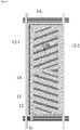
- FIG. 6 is a schematic diagram illustrating the structure of a liquid crystal display panel not according to the invention.
- FIG. 7 is a cross-sectional view along C-C' line of the liquid crystal display panel in FIG. 6 .
- FIG. 8 is a cross-sectional view along D-D' line of the liquid crystal display panel in FIG. 6 .
- the liquid crystal display panel in each subpixel, includes a first electrode layer 11, a second electrode layer 12, and an insulating layer 13 between the first electrode layer 11 and the second electrode layer 12.
- the first electrode layer 11 and the second electrode layer 12 are configured to form a fringe field for driving liquid crystal molecules in the liquid crystal layer 3.
- the second electrode layer 12 is a common electrode layer
- the first electrode layer 11 is a pixel electrode layer
- the first electrode layer 11 is connected to the drain electrode of the switching thin film transistor.
- the first electrode layer 11 (e.g., a common electrode layer) is a plate electrode layer that extends substantially throughout the subpixel area, e.g., extending to a first edge of the subpixel (e.g., proximal to the C-C' line in FIG. 6 ).
- the second electrode layer 12 includes a plurality of branches 12B (e.g., a first branch 12B1 and a second branch 12B2 in FIG. 6 ), each of which extends substantially along a longitudinal direction of the subpixel.
- the plurality of branches 12B are spaced apart by a plurality of slits (e.g., a first slit S1 and a second slit S2 in FIG. 6 ).
- the plurality of branches 12B may be grouped into a plurality of teeth T.
- each of the plurality of teeth T includes a first branch 12B1 and a second branch 12B2 of the plurality of branches 12B.
- the first branch 12B1 and the second branch 12B2 are connected to each other along the first edge of the subpixel proximal to the C-C' line in FIG. 6 .
- Adjacent teeth of the plurality of teeth T are spaced apart by a first slit S1.
- the first branch 12B1 and the second branch 12B2 in each of the plurality of teeth T are spaced apart by a second slit S2.
- the first slit S1 is open at a first end E1 (e.g., the end proximal to a first signal line along a first edge of the subpixel), and closed at a second end E2 (e.g., the end proximal to a second signal line along a second edge of the subpixel, the second edge opposite to the first edge).
- the first end E1 is opposite to the second end E2.
- the first slit S1 extends along a direction substantially parallel to the adjacent teeth (or adjacent branches 12B in an embodiment depicted in FIG.
- the first slit S1 extends substantially throughout one dimension of the second electrode layer 12, e.g., throughout the longitudinal dimension of the second electrode layer 12. Adjacent teeth are separated from each other at the first end E1 and connected to each other at the second end E2.
- the second slit S2 is closed at a third end E3 (e.g., the end proximal to a first signal line along a first edge of the subpixel) and open at a fourth end E4 (e.g., the end proximal to a second signal line along a second edge of the subpixel, the second edge opposite to the first edge).
- the third end E3 is opposite to the fourth end E4.
- the second slit S2 extends along a direction substantially parallel to the first branch 12B1 and the second branch 12B2 in each of the plurality of teeth T, the third end E3 of the second slit S2 proximal to a first end of one of the plurality of teeth T and distal to a second end of the one of the plurality of teeth T opposite to the first end of the one of the plurality of teeth T; and the fourth end E4 of the second slit S2 proximal to the second end of one of the plurality of teeth T and distal to the first end of the one of the plurality of teeth T.
- the second slit S2 extends substantially throughout the one dimension of the second electrode layer 12, e.g., throughout the longitudinal dimension of the second electrode layer 12.
- the second slit S2 is substantially parallel to the first slit S1.
- the third end E3 is proximal to the first end E1 and distal to the second end E2, and the fourth end E4 is proximal to the second end E2 and distal to the first end E1.
- the first branch 12B1 and the second branch 12B2 are separated from each other at the fourth end E4 and connected to each other at the third end E3.
- the second electrode layer 12 is a zig-zag shaped electrode layer.
- the liquid crystal display panel includes a plurality of teeth T.
- the present liquid crystal display panel includes multiple slits along both edges of the subpixel.
- the liquid crystal display panel depicted in FIGs. 6 to 8 has greatly reduced overlapping areas between the first electrode layer 11 and the second electrode layer 12.
- the storage capacitance between the first electrode layer 11 and the second electrode layer 12 is much reduced.
- light transmittance along the edges of the subpixels is significantly improved, obviating the issue of dark areas along the edges of the subpixels.
- the plurality of branches extend substantially along a longitudinal direction of the subpixel.
- the plurality of branches extend substantially along a lateral direction of the subpixel.
- the first electrode layer 11 and the second electrode layer 12 are both in the array substrate 1.
- each of the plurality of branches 12B extends substantially throughout one dimension (e.g., the longitudinal dimension) of the second electrode layer 12. Any structure connecting the adjacent teeth or adjacent branches is disposed in peripheral regions of the second electrode layer 12.
- the first end E1 and the second end E2 of the first slit S1, and the third end E3 and the fourth end E4 of the second slit S2 are in peripheral regions of the second electrode layer 12.
- the second electrode layer 12 is a single domain electrode layer.
- the second electrode layer 12 is a multi-domain electrode layer.
- the second electrode layer 12 includes a first domain and a second domain, branches and slits in the first domain extending substantially along a first direction, and branches and slits in the second domain extending substantially along a second direction.
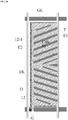
- FIG. 9 is a schematic diagram illustrating the structure of a conventional liquid crystal display panel.
- the conventional liquid crystal display panel in each subpixel includes a first electrode layer 11 and a second electrode layer 12.
- the second electrode layer 12 in some embodiments includes a first domain (the top domain) and a second domain (the bottom domain).
- the second electrode layer 12 includes a plurality of branches 12B spaced apart by a plurality of slits S.
- the plurality of branches 12B in the first domain extend substantially along a first direction.
- the plurality of branches 12B in the second domain extend substantially along a second direction.
- the plurality of branches 12B are connected together by a first bar 12-1 on the left side of the second electrode layer 12 and a second bar 12-2 on the right side of the second electrode layer 12.
- Each of the plurality of slits S has a first end and a second end, both of which are closed ends.
- the first bar 12-1 and the second bar 12-2 close each of the plurality of slits S at its first end and the second end.
- the first electrode layer 11 extends to the edges of the subpixel. A projection of the first electrode layer 11 on the base substrate 10 overlaps with that of the first bar 12-1 of the second electrode layer 12 throughout the length of the first electrode layer 11 along the edge of the subpixel.
- FIG. 10 is a schematic diagram illustrating the structure of a liquid crystal display panel not according to the invention.
- the first electrode layer 11 e.g., a common electrode layer
- the second electrode layer 12 includes a plurality of branches 12B, each of which extends substantially along a lateral direction of the subpixel.
- the plurality of branches 12B are spaced apart by a plurality of slits (e.g., a first slit S1 in FIG. 10 ).
- the plurality of branches 12B may be grouped into a plurality of teeth T.
- each of the plurality of branches 12B corresponds to one of the plurality of teeth T, e.g., each of the plurality of teeth T includes only one of the plurality of branches 12B. Adjacent teeth of the plurality of teeth T are spaced apart by a first slit S1. Thus, in the embodiment depicted in FIG. 10 , adjacent branches of the plurality of branches 12B are spaced apart by a first slit S1.
- the first slit S1 is open at a first end E1 (e.g., the end proximal to a first signal line along a first edge of the subpixel), and closed at a second end E2 (e.g., the end proximal to a second signal line along a second edge of the subpixel, the second edge opposite to the first edge).
- the first end E1 is opposite to the second end E2.
- the first slit S1 extends along a direction substantially parallel to the adjacent teeth (or adjacent branches in an embodiment depicted in FIG.
- first end E1 of the first slit S1 proximal to a first end of one of the plurality of branches 12B and distal to a second end of the one of the plurality of branches 12B opposite to the first end of the one of the plurality of branches 12B; and the second end E2 of the first slit S1 proximal to the second end of one of the plurality of branches 12B and distal to the first end of the one of the plurality of branches 12B.
- the first slit S1 extends substantially throughout one dimension of the second electrode layer 12, e.g., throughout the lateral dimension of the second electrode layer 12. Adjacent teeth are separated from each other at the first end E1 and connected to each other at the second end E2. In the embodiments depicted in FIG. 10 , adjacent branches of the plurality of branches 12B are separated from each other at the first end E1 and connected to each other at the second end E2.
- the second electrode layer 12 depicted in FIG. 10 is a comb-shaped electrode layer having a plurality of teeth T and a bar (e.g., a first bar 12-1 as shown in FIG. 10 ) connecting the adjacent teeth of the plurality of teeth T at the second end E2.
- Each of the plurality of branches 12B extends substantially throughout one dimension (e.g., the lateral dimension) of the second electrode layer 12. Any structure connecting the adjacent teeth or adjacent branches is disposed in peripheral regions of the second electrode layer 12.
- the first end E1 and the second end E2 of the first slit S1 are in peripheral regions of the second electrode layer 12.
- the bar connecting the adjacent teeth of the plurality of teeth is also in a peripheral region of the second electrode layer 12.
- FIG. 11 is a schematic diagram illustrating the structure of a liquid crystal display panel not according to the invention.
- the bar connecting the adjacent teeth or adjacent branches is a second bar 12-2 along an edge on the right side of the subpixel. Similar to FIG. 10 , the overlapping area and storage capacitance between the first electrode layer 11 and the second electrode layer 12 are significantly reduced as compared to conventional liquid crystal display panels. Light transmittance along the edges of the subpixels is enhanced, eliminating dark edges in image display.
- FIG. 12 is a schematic diagram illustrating the structure of a liquid crystal display panel not according to the invention.
- the second electrode layer 12 includes a plurality of branches 12B (e.g., a first branch 12B1 and a second branch 12B2 in FIG. 12 ), each of which extends substantially along a lateral direction of the subpixel.
- the plurality of branches 12B are spaced apart by a plurality of slits (e.g., a first slit S1 and a second slit S2 in FIG. 12 ).
- the plurality of branches 12B are grouped into a plurality of teeth T, for example, in FIG.
- each of the plurality of teeth T includes a first branch 12B1 and a second branch 12B2 of the plurality of branches 12B.
- the first branch 12B1 and the second branch 12B2 are connected to each other along the right edge of the subpixel. Adjacent teeth of the plurality of teeth T are spaced apart by a first slit S1.
- the first branch 12B1 and the second branch 12B2 in each of the plurality of teeth T are spaced apart by a second slit S2.
- the first slit S1 is open at a first end E1 and closed at a second end E2, the first end E1 being opposite to the second end E2.
- the first slit S1 extends along a direction substantially parallel to the adjacent teeth or adjacent branches.
- the first slit S1 extends substantially throughout one dimension of the second electrode layer 12, e.g., throughout the lateral dimension of the second electrode layer 12. Adjacent teeth are separated from each other at the first end E1 and connected to each other at the second end E2.
- the second slit S2 is closed at a third end E3 and open at a fourth end E4, the third end E3 being opposite to the fourth end E4.
- the second slit S2 extends along a direction substantially parallel to the first branch 12B1 and the second branch 12B2 in each of the plurality of teeth T.
- the second slit S2 extends substantially throughout the one dimension of the second electrode layer 12, e.g., throughout the lateral dimension of the second electrode layer 12.
- the second slit S2 is substantially parallel to the first slit S1.
- the third end E3 is proximal to the first end E1 and distal to the second end E2, and the fourth end E4 is proximal to the second end E2 and distal to the first end E1.
- the first branch 12B1 and the second branch 12B2 are separated from each other at the fourth end E4 and connected to each other at the third end E3.
- the second electrode layer 12 in FIG. 12 is a zig-zag shaped electrode layer.
- the liquid crystal display panel includes a plurality of teeth T.
- each of the plurality of branches 12B extends substantially throughout one dimension (e.g., the lateral dimension) of the second electrode layer 12. Any structure connecting the adjacent teeth or adjacent branches is disposed in peripheral regions of the second electrode layer 12.
- the first end E1 and the second end E2 of the first slit S1, and the third end E3 and the fourth end E4 of the second slit S2 are in peripheral regions of the second electrode layer 12.
- the liquid crystal display panel is a fringe field driven liquid crystal display panel, in which the liquid crystal layer is driven by a fringe electric field.
- fringe field driven liquid crystal display panel include, but are not limited to, an advanced super-dimensional switching (ADS) liquid crystal display panel, and a fringe field switching (FFS) liquid crystal display panel.
- ADS advanced super-dimensional switching
- FFS fringe field switching
- the present disclosure provides a liquid crystal display apparatus having a liquid crystal display panel described herein.
- appropriate display apparatuses include, but are not limited to a mobile phone, a tablet computer, a television, a monitor, a notebook computer, a digital album, a gaming system, etc.
Landscapes
- Physics & Mathematics (AREA)
- Nonlinear Science (AREA)
- Geometry (AREA)
- Mathematical Physics (AREA)
- Chemical & Material Sciences (AREA)
- Crystallography & Structural Chemistry (AREA)
- General Physics & Mathematics (AREA)
- Optics & Photonics (AREA)
- Liquid Crystal (AREA)
Claims (8)
- Array-Substrat (1), aufweisend eine Vielzahl von Subpixelbereichen, wobei das Array-Substrat (1) in jedem der Vielzahl von Subpixelbereichen Folgendes umfasst:eine erste Elektrodenschicht (11) und eine zweite Elektrodenschicht (12), die so konfiguriert sind, dass sie ein Streufeld zum Ansteuern von Flüssigkristallmolekülen bilden;eine Isolierschicht (13) zwischen der ersten Elektrodenschicht (11) und der zweiten Elektrodenschicht (12); undeine gemeinsame Elektroden-Signalleitung (CL);wobei die zweite Elektrodenschicht (12) eine kammförmige Elektrode ist und eine Vielzahl von Verzweigungen (12B) umfasst;wobei die Zähne so definiert sind, dass jeder der Vielzahl von Zähnen (T) nur einen der Vielzahl von Verzweigungen umfasst;wobei benachbarte Zähne (T) der Vielzahl von Zähnen (T) durch einen ersten Schlitz (S1) voneinander beabstandet sind, wobei sich der erste Schlitz (S1) im Wesentlichen durch eine Dimension der zweiten Elektrodenschicht (12) von einem der Vielzahl von Subpixelbereichen erstreckt;wobei die benachbarten Zähne (T) an ihrem ersten Ende (E1) voneinander getrennt und an ihrem zweiten Ende (E2) miteinander verbunden sind;wobei die zweite Elektrodenschicht (12) weiter einen Stab aufweist, der die benachbarten Zähne (T) der Vielzahl von Zähnen (T) an ihrem zweiten Ende (E2) verbindet;wobei der Stab in einem Randbereich der zweiten Elektrodenschicht (12) gelegen ist; unddadurch gekennzeichnet, dasseine Projektion der gemeinsamen Elektroden-Signalleitung (CL) auf einem Basissubstrat (10) des Array-Substrats (1) zumindest teilweise mit Projektionen der Vielzahl von Zähnen (T) an ihren ersten Enden (E1) auf dem Basissubstrat (10) überlappt.
- Array-Substrat (1) nach Anspruch 1, wobei die erste Elektrodenschicht (11) eine Plattenelektrodenschicht ist, die sich im Wesentlichen über einen der Vielzahl von Subpixelbereichen erstreckt.
- Array-Substrat (1) nach Anspruch 1, wobei sich das erste Ende (E1) und das zweite Ende (E2) in peripheren Bereichen der zweiten Elektrodenschicht (12) befinden.
- Array-Substrat nach Anspruch 1, wobei sich die Vielzahl von Verzweigungen (12B) im Wesentlichen entlang einer Längsrichtung des Subpixelbereichs erstreckt.
- Array-Substrat (1) nach Anspruch 1, wobei die erste Elektrodenschicht (11) eine gemeinsame Elektrodenschicht ist und die zweite Elektrodenschicht (12) eine Pixelelektrodenschicht ist;
oder
wobei die zweite Elektrodenschicht (12) eine gemeinsame Elektrodenschicht ist, und die erste Elektrodenschicht (11) eine Pixelelektrodenschicht ist. - Flüssigkristall-Anzeigetafel, umfassend:das Array-Substrat (1) nach einem der Ansprüche 1 bis 5;ein Gegensubstrat (2), das dem Array-Substrat (1) gegenüberliegt; undeine Flüssigkristallschicht (3) zwischen dem Array-Substrat (1) und dem Gegensubstrat (2).
- Flüssigkristall-Anzeigetafel nach Anspruch 6, wobei die Flüssigkristall-Anzeigetafel eine mittels Streufeld angesteuerte Flüssigkristall-Anzeigetafel ist, bei der Flüssigkristallmoleküle in der Flüssigkristallschicht (3) durch ein elektrisches Streufeld angesteuert werden.
- Flüssigkristall-Anzeigeeinrichtung, die die Flüssigkristall-Anzeigetafel nach einem der Ansprüche 6 bis 7 umfasst.
Applications Claiming Priority (1)
| Application Number | Priority Date | Filing Date | Title |
|---|---|---|---|
| PCT/CN2017/079339 WO2018176483A1 (en) | 2017-04-01 | 2017-04-01 | Array substrate, liquid crystal display panel and liquid crystal display apparatus |
Publications (3)
| Publication Number | Publication Date |
|---|---|
| EP3607398A1 EP3607398A1 (de) | 2020-02-12 |
| EP3607398A4 EP3607398A4 (de) | 2020-09-02 |
| EP3607398B1 true EP3607398B1 (de) | 2022-01-12 |
Family
ID=63674058
Family Applications (1)
| Application Number | Title | Priority Date | Filing Date |
|---|---|---|---|
| EP17903368.3A Active EP3607398B1 (de) | 2017-04-01 | 2017-04-01 | Arraysubstrat, flüssigkristallanzeigetafel und flüssigkristallanzeigevorrichtung |
Country Status (5)
| Country | Link |
|---|---|
| US (1) | US20200249534A1 (de) |
| EP (1) | EP3607398B1 (de) |
| JP (1) | JP7004734B2 (de) |
| CN (1) | CN109154749A (de) |
| WO (1) | WO2018176483A1 (de) |
Families Citing this family (2)
| Publication number | Priority date | Publication date | Assignee | Title |
|---|---|---|---|---|
| US12032248B2 (en) | 2022-02-10 | 2024-07-09 | Shanghai Tianma Micro-electronics Co., Ltd. | Liquid crystal display panel and liquid crystal display device |
| CN114660856B (zh) | 2022-03-16 | 2024-02-20 | Tcl华星光电技术有限公司 | 阵列基板及显示装置 |
Family Cites Families (18)
| Publication number | Priority date | Publication date | Assignee | Title |
|---|---|---|---|---|
| TW387997B (en) * | 1997-12-29 | 2000-04-21 | Hyundai Electronics Ind | Liquid crystal display and fabrication method |
| KR100325065B1 (ko) * | 1998-06-30 | 2002-08-24 | 주식회사 현대 디스플레이 테크놀로지 | 고휘도및광시야각을갖는반사형액정표시장치 |
| KR20000039794A (ko) * | 1998-12-16 | 2000-07-05 | 김영환 | 고개구율 및 고투과율 액정표시장치의 제조방법 |
| KR100494682B1 (ko) * | 1999-06-30 | 2005-06-13 | 비오이 하이디스 테크놀로지 주식회사 | 액정표시소자 및 그 제조방법 |
| KR100500684B1 (ko) * | 1999-12-29 | 2005-07-12 | 비오이 하이디스 테크놀로지 주식회사 | 4-마스크 공정을 이용한 액정 디스플레이의 제조 방법 |
| JP2007327997A (ja) * | 2006-06-06 | 2007-12-20 | Epson Imaging Devices Corp | 液晶装置、及び電子機器 |
| CN100565313C (zh) * | 2006-09-15 | 2009-12-02 | 爱普生映像元器件有限公司 | 液晶显示板 |
| JP4201051B2 (ja) * | 2006-09-15 | 2008-12-24 | エプソンイメージングデバイス株式会社 | 液晶表示パネル |
| JP4600463B2 (ja) * | 2007-11-21 | 2010-12-15 | ソニー株式会社 | 液晶表示装置 |
| KR20090116856A (ko) * | 2008-05-08 | 2009-11-12 | 전북대학교산학협력단 | 프린지 인플레인 필드 스위칭 액정표시소자 |
| CN101995700B (zh) * | 2009-08-10 | 2012-07-18 | 北京京东方光电科技有限公司 | 液晶面板及其制造方法 |
| US8953132B2 (en) * | 2011-03-30 | 2015-02-10 | Au Optronics Corp. | Pixel array of fringe field switching liquid crystal display panel and driving method thereof |
| CN103185993B (zh) * | 2011-12-29 | 2016-06-22 | 上海天马微电子有限公司 | Ips/ffs型液晶显示装置的阵列基板 |
| CN102789106B (zh) * | 2012-04-24 | 2015-01-07 | 京东方科技集团股份有限公司 | 有机薄膜晶体管阵列基板及其制备方法以及显示装置 |
| JP2014228565A (ja) * | 2013-05-17 | 2014-12-08 | パナソニック液晶ディスプレイ株式会社 | 液晶表示装置及び液晶表示装置の製造方法 |
| CN203894515U (zh) * | 2014-06-13 | 2014-10-22 | 京东方科技集团股份有限公司 | 一种阵列基板及显示装置 |
| CN105137680B (zh) * | 2015-10-20 | 2018-11-06 | 京东方科技集团股份有限公司 | 一种液晶显示用电极、阵列基板、显示面板、显示装置 |
| CN105676550A (zh) * | 2016-04-21 | 2016-06-15 | 京东方科技集团股份有限公司 | 阵列基板及其制造方法、显示装置 |
-
2017
- 2017-04-01 EP EP17903368.3A patent/EP3607398B1/de active Active
- 2017-04-01 WO PCT/CN2017/079339 patent/WO2018176483A1/en not_active Ceased
- 2017-04-01 JP JP2019548984A patent/JP7004734B2/ja active Active
- 2017-04-01 CN CN201780000183.9A patent/CN109154749A/zh active Pending
- 2017-04-01 US US15/761,347 patent/US20200249534A1/en not_active Abandoned
Also Published As
| Publication number | Publication date |
|---|---|
| WO2018176483A9 (en) | 2018-11-15 |
| JP2020513111A (ja) | 2020-04-30 |
| US20200249534A1 (en) | 2020-08-06 |
| EP3607398A1 (de) | 2020-02-12 |
| JP7004734B2 (ja) | 2022-02-10 |
| WO2018176483A1 (en) | 2018-10-04 |
| EP3607398A4 (de) | 2020-09-02 |
| CN109154749A (zh) | 2019-01-04 |
Similar Documents
| Publication | Publication Date | Title |
|---|---|---|
| TWI509482B (zh) | 內建觸控面板型顯示裝置 | |
| JP5875001B2 (ja) | 横電界方式の液晶表示装置 | |
| CN103309093B (zh) | 液晶显示装置 | |
| JP3723911B2 (ja) | フリンジフィールド駆動液晶表示装置 | |
| EP3358613B1 (de) | Arraysubstrat und herstellungsverfahren dafür und anzeigevorrichtung | |
| EP2650763A2 (de) | Anzeigevorrichtung und Verfahren zu ihrer Herstellung | |
| CN111103734A (zh) | 阵列基板、显示面板和显示装置 | |
| US9196634B2 (en) | TFT array substrate, display panel and display device | |
| EP3709078B1 (de) | Anzeigesubstrat, herstellungsverfahren dafür und anzeigetafel | |
| US10317737B2 (en) | Array substrate, display panel and display device | |
| EP3702834B1 (de) | Arraysubstrat und anzeigevorrichtung | |
| JP5127485B2 (ja) | 液晶表示装置 | |
| KR101323412B1 (ko) | 액정표시장치 및 그 제조 방법 | |
| JP4999875B2 (ja) | 多重ドメイン液晶表示装置 | |
| CN103529575A (zh) | 液晶显示装置 | |
| US10877327B2 (en) | Pixel structure | |
| CN111580309B (zh) | 一种阵列基板、显示面板 | |
| US6850304B2 (en) | In-plane switching mode liquid crystal display with a compensation electrode structure and method of forming the same | |
| CN110245646A (zh) | 显示面板和显示装置 | |
| EP3607398B1 (de) | Arraysubstrat, flüssigkristallanzeigetafel und flüssigkristallanzeigevorrichtung | |
| CN108490705B (zh) | 阵列基板、液晶显示面板与显示装置 | |
| US9726941B2 (en) | Pixel unit, array substrate, display device, and pixel driving method | |
| CN103207483B (zh) | 液晶显示装置 | |
| CN107144999B (zh) | 内嵌式触摸屏 | |
| KR20170041929A (ko) | 액정 표시 장치 |
Legal Events
| Date | Code | Title | Description |
|---|---|---|---|
| STAA | Information on the status of an ep patent application or granted ep patent |
Free format text: STATUS: THE INTERNATIONAL PUBLICATION HAS BEEN MADE |
|
| PUAI | Public reference made under article 153(3) epc to a published international application that has entered the european phase |
Free format text: ORIGINAL CODE: 0009012 |
|
| STAA | Information on the status of an ep patent application or granted ep patent |
Free format text: STATUS: REQUEST FOR EXAMINATION WAS MADE |
|
| 17P | Request for examination filed |
Effective date: 20190830 |
|
| AK | Designated contracting states |
Kind code of ref document: A1 Designated state(s): AL AT BE BG CH CY CZ DE DK EE ES FI FR GB GR HR HU IE IS IT LI LT LU LV MC MK MT NL NO PL PT RO RS SE SI SK SM TR |
|
| AX | Request for extension of the european patent |
Extension state: BA ME |
|
| DAV | Request for validation of the european patent (deleted) | ||
| DAX | Request for extension of the european patent (deleted) | ||
| A4 | Supplementary search report drawn up and despatched |
Effective date: 20200803 |
|
| RIC1 | Information provided on ipc code assigned before grant |
Ipc: G02F 1/1343 20060101AFI20200728BHEP |
|
| GRAP | Despatch of communication of intention to grant a patent |
Free format text: ORIGINAL CODE: EPIDOSNIGR1 |
|
| STAA | Information on the status of an ep patent application or granted ep patent |
Free format text: STATUS: GRANT OF PATENT IS INTENDED |
|
| INTG | Intention to grant announced |
Effective date: 20210805 |
|
| GRAS | Grant fee paid |
Free format text: ORIGINAL CODE: EPIDOSNIGR3 |
|
| GRAA | (expected) grant |
Free format text: ORIGINAL CODE: 0009210 |
|
| STAA | Information on the status of an ep patent application or granted ep patent |
Free format text: STATUS: THE PATENT HAS BEEN GRANTED |
|
| AK | Designated contracting states |
Kind code of ref document: B1 Designated state(s): AL AT BE BG CH CY CZ DE DK EE ES FI FR GB GR HR HU IE IS IT LI LT LU LV MC MK MT NL NO PL PT RO RS SE SI SK SM TR |
|
| REG | Reference to a national code |
Ref country code: GB Ref legal event code: FG4D |
|
| REG | Reference to a national code |
Ref country code: CH Ref legal event code: EP |
|
| REG | Reference to a national code |
Ref country code: DE Ref legal event code: R096 Ref document number: 602017052402 Country of ref document: DE |
|
| REG | Reference to a national code |
Ref country code: IE Ref legal event code: FG4D |
|
| REG | Reference to a national code |
Ref country code: AT Ref legal event code: REF Ref document number: 1462777 Country of ref document: AT Kind code of ref document: T Effective date: 20220215 |
|
| REG | Reference to a national code |
Ref country code: LT Ref legal event code: MG9D |
|
| REG | Reference to a national code |
Ref country code: NL Ref legal event code: MP Effective date: 20220112 |
|
| REG | Reference to a national code |
Ref country code: AT Ref legal event code: MK05 Ref document number: 1462777 Country of ref document: AT Kind code of ref document: T Effective date: 20220112 |
|
| PG25 | Lapsed in a contracting state [announced via postgrant information from national office to epo] |
Ref country code: NL Free format text: LAPSE BECAUSE OF FAILURE TO SUBMIT A TRANSLATION OF THE DESCRIPTION OR TO PAY THE FEE WITHIN THE PRESCRIBED TIME-LIMIT Effective date: 20220112 |
|
| PG25 | Lapsed in a contracting state [announced via postgrant information from national office to epo] |
Ref country code: SE Free format text: LAPSE BECAUSE OF FAILURE TO SUBMIT A TRANSLATION OF THE DESCRIPTION OR TO PAY THE FEE WITHIN THE PRESCRIBED TIME-LIMIT Effective date: 20220112 Ref country code: RS Free format text: LAPSE BECAUSE OF FAILURE TO SUBMIT A TRANSLATION OF THE DESCRIPTION OR TO PAY THE FEE WITHIN THE PRESCRIBED TIME-LIMIT Effective date: 20220112 Ref country code: PT Free format text: LAPSE BECAUSE OF FAILURE TO SUBMIT A TRANSLATION OF THE DESCRIPTION OR TO PAY THE FEE WITHIN THE PRESCRIBED TIME-LIMIT Effective date: 20220512 Ref country code: NO Free format text: LAPSE BECAUSE OF FAILURE TO SUBMIT A TRANSLATION OF THE DESCRIPTION OR TO PAY THE FEE WITHIN THE PRESCRIBED TIME-LIMIT Effective date: 20220412 Ref country code: LT Free format text: LAPSE BECAUSE OF FAILURE TO SUBMIT A TRANSLATION OF THE DESCRIPTION OR TO PAY THE FEE WITHIN THE PRESCRIBED TIME-LIMIT Effective date: 20220112 Ref country code: HR Free format text: LAPSE BECAUSE OF FAILURE TO SUBMIT A TRANSLATION OF THE DESCRIPTION OR TO PAY THE FEE WITHIN THE PRESCRIBED TIME-LIMIT Effective date: 20220112 Ref country code: ES Free format text: LAPSE BECAUSE OF FAILURE TO SUBMIT A TRANSLATION OF THE DESCRIPTION OR TO PAY THE FEE WITHIN THE PRESCRIBED TIME-LIMIT Effective date: 20220112 Ref country code: BG Free format text: LAPSE BECAUSE OF FAILURE TO SUBMIT A TRANSLATION OF THE DESCRIPTION OR TO PAY THE FEE WITHIN THE PRESCRIBED TIME-LIMIT Effective date: 20220412 |
|
| PG25 | Lapsed in a contracting state [announced via postgrant information from national office to epo] |
Ref country code: PL Free format text: LAPSE BECAUSE OF FAILURE TO SUBMIT A TRANSLATION OF THE DESCRIPTION OR TO PAY THE FEE WITHIN THE PRESCRIBED TIME-LIMIT Effective date: 20220112 Ref country code: LV Free format text: LAPSE BECAUSE OF FAILURE TO SUBMIT A TRANSLATION OF THE DESCRIPTION OR TO PAY THE FEE WITHIN THE PRESCRIBED TIME-LIMIT Effective date: 20220112 Ref country code: GR Free format text: LAPSE BECAUSE OF FAILURE TO SUBMIT A TRANSLATION OF THE DESCRIPTION OR TO PAY THE FEE WITHIN THE PRESCRIBED TIME-LIMIT Effective date: 20220413 Ref country code: FI Free format text: LAPSE BECAUSE OF FAILURE TO SUBMIT A TRANSLATION OF THE DESCRIPTION OR TO PAY THE FEE WITHIN THE PRESCRIBED TIME-LIMIT Effective date: 20220112 Ref country code: AT Free format text: LAPSE BECAUSE OF FAILURE TO SUBMIT A TRANSLATION OF THE DESCRIPTION OR TO PAY THE FEE WITHIN THE PRESCRIBED TIME-LIMIT Effective date: 20220112 |
|
| PG25 | Lapsed in a contracting state [announced via postgrant information from national office to epo] |
Ref country code: IS Free format text: LAPSE BECAUSE OF FAILURE TO SUBMIT A TRANSLATION OF THE DESCRIPTION OR TO PAY THE FEE WITHIN THE PRESCRIBED TIME-LIMIT Effective date: 20220512 |
|
| REG | Reference to a national code |
Ref country code: DE Ref legal event code: R097 Ref document number: 602017052402 Country of ref document: DE |
|
| PG25 | Lapsed in a contracting state [announced via postgrant information from national office to epo] |
Ref country code: SM Free format text: LAPSE BECAUSE OF FAILURE TO SUBMIT A TRANSLATION OF THE DESCRIPTION OR TO PAY THE FEE WITHIN THE PRESCRIBED TIME-LIMIT Effective date: 20220112 Ref country code: SK Free format text: LAPSE BECAUSE OF FAILURE TO SUBMIT A TRANSLATION OF THE DESCRIPTION OR TO PAY THE FEE WITHIN THE PRESCRIBED TIME-LIMIT Effective date: 20220112 Ref country code: RO Free format text: LAPSE BECAUSE OF FAILURE TO SUBMIT A TRANSLATION OF THE DESCRIPTION OR TO PAY THE FEE WITHIN THE PRESCRIBED TIME-LIMIT Effective date: 20220112 Ref country code: EE Free format text: LAPSE BECAUSE OF FAILURE TO SUBMIT A TRANSLATION OF THE DESCRIPTION OR TO PAY THE FEE WITHIN THE PRESCRIBED TIME-LIMIT Effective date: 20220112 Ref country code: DK Free format text: LAPSE BECAUSE OF FAILURE TO SUBMIT A TRANSLATION OF THE DESCRIPTION OR TO PAY THE FEE WITHIN THE PRESCRIBED TIME-LIMIT Effective date: 20220112 Ref country code: CZ Free format text: LAPSE BECAUSE OF FAILURE TO SUBMIT A TRANSLATION OF THE DESCRIPTION OR TO PAY THE FEE WITHIN THE PRESCRIBED TIME-LIMIT Effective date: 20220112 |
|
| PLBE | No opposition filed within time limit |
Free format text: ORIGINAL CODE: 0009261 |
|
| STAA | Information on the status of an ep patent application or granted ep patent |
Free format text: STATUS: NO OPPOSITION FILED WITHIN TIME LIMIT |
|
| PG25 | Lapsed in a contracting state [announced via postgrant information from national office to epo] |
Ref country code: AL Free format text: LAPSE BECAUSE OF FAILURE TO SUBMIT A TRANSLATION OF THE DESCRIPTION OR TO PAY THE FEE WITHIN THE PRESCRIBED TIME-LIMIT Effective date: 20220112 |
|
| REG | Reference to a national code |
Ref country code: CH Ref legal event code: PL |
|
| 26N | No opposition filed |
Effective date: 20221013 |
|
| GBPC | Gb: european patent ceased through non-payment of renewal fee |
Effective date: 20220412 |
|
| REG | Reference to a national code |
Ref country code: BE Ref legal event code: MM Effective date: 20220430 |
|
| PG25 | Lapsed in a contracting state [announced via postgrant information from national office to epo] |
Ref country code: MC Free format text: LAPSE BECAUSE OF FAILURE TO SUBMIT A TRANSLATION OF THE DESCRIPTION OR TO PAY THE FEE WITHIN THE PRESCRIBED TIME-LIMIT Effective date: 20220112 Ref country code: LU Free format text: LAPSE BECAUSE OF NON-PAYMENT OF DUE FEES Effective date: 20220401 Ref country code: LI Free format text: LAPSE BECAUSE OF NON-PAYMENT OF DUE FEES Effective date: 20220430 Ref country code: GB Free format text: LAPSE BECAUSE OF NON-PAYMENT OF DUE FEES Effective date: 20220412 Ref country code: FR Free format text: LAPSE BECAUSE OF NON-PAYMENT OF DUE FEES Effective date: 20220430 Ref country code: CH Free format text: LAPSE BECAUSE OF NON-PAYMENT OF DUE FEES Effective date: 20220430 |
|
| PG25 | Lapsed in a contracting state [announced via postgrant information from national office to epo] |
Ref country code: SI Free format text: LAPSE BECAUSE OF FAILURE TO SUBMIT A TRANSLATION OF THE DESCRIPTION OR TO PAY THE FEE WITHIN THE PRESCRIBED TIME-LIMIT Effective date: 20220112 Ref country code: BE Free format text: LAPSE BECAUSE OF NON-PAYMENT OF DUE FEES Effective date: 20220430 |
|
| PG25 | Lapsed in a contracting state [announced via postgrant information from national office to epo] |
Ref country code: IE Free format text: LAPSE BECAUSE OF NON-PAYMENT OF DUE FEES Effective date: 20220401 |
|
| PG25 | Lapsed in a contracting state [announced via postgrant information from national office to epo] |
Ref country code: IT Free format text: LAPSE BECAUSE OF FAILURE TO SUBMIT A TRANSLATION OF THE DESCRIPTION OR TO PAY THE FEE WITHIN THE PRESCRIBED TIME-LIMIT Effective date: 20220112 |
|
| PG25 | Lapsed in a contracting state [announced via postgrant information from national office to epo] |
Ref country code: MK Free format text: LAPSE BECAUSE OF FAILURE TO SUBMIT A TRANSLATION OF THE DESCRIPTION OR TO PAY THE FEE WITHIN THE PRESCRIBED TIME-LIMIT Effective date: 20220112 Ref country code: CY Free format text: LAPSE BECAUSE OF FAILURE TO SUBMIT A TRANSLATION OF THE DESCRIPTION OR TO PAY THE FEE WITHIN THE PRESCRIBED TIME-LIMIT Effective date: 20220112 |
|
| PG25 | Lapsed in a contracting state [announced via postgrant information from national office to epo] |
Ref country code: HU Free format text: LAPSE BECAUSE OF FAILURE TO SUBMIT A TRANSLATION OF THE DESCRIPTION OR TO PAY THE FEE WITHIN THE PRESCRIBED TIME-LIMIT; INVALID AB INITIO Effective date: 20170401 |
|
| PG25 | Lapsed in a contracting state [announced via postgrant information from national office to epo] |
Ref country code: TR Free format text: LAPSE BECAUSE OF FAILURE TO SUBMIT A TRANSLATION OF THE DESCRIPTION OR TO PAY THE FEE WITHIN THE PRESCRIBED TIME-LIMIT Effective date: 20220112 |
|
| PG25 | Lapsed in a contracting state [announced via postgrant information from national office to epo] |
Ref country code: MT Free format text: LAPSE BECAUSE OF FAILURE TO SUBMIT A TRANSLATION OF THE DESCRIPTION OR TO PAY THE FEE WITHIN THE PRESCRIBED TIME-LIMIT Effective date: 20220112 |
|
| PGFP | Annual fee paid to national office [announced via postgrant information from national office to epo] |
Ref country code: DE Payment date: 20250422 Year of fee payment: 9 |