EP3691024B1 - Verlustarme und flexible, gekrümmte oder orthogonale übertragungsleitungsintegrierte mehrfachanschlussantenne für millimeterwellenband - Google Patents
Verlustarme und flexible, gekrümmte oder orthogonale übertragungsleitungsintegrierte mehrfachanschlussantenne für millimeterwellenband Download PDFInfo
- Publication number
- EP3691024B1 EP3691024B1 EP20154341.0A EP20154341A EP3691024B1 EP 3691024 B1 EP3691024 B1 EP 3691024B1 EP 20154341 A EP20154341 A EP 20154341A EP 3691024 B1 EP3691024 B1 EP 3691024B1
- Authority
- EP
- European Patent Office
- Prior art keywords
- antenna
- transmission line
- loss
- low
- integrated
- Prior art date
- Legal status (The legal status is an assumption and is not a legal conclusion. Google has not performed a legal analysis and makes no representation as to the accuracy of the status listed.)
- Active
Links
Images














Classifications
-
- H—ELECTRICITY
- H01—ELECTRIC ELEMENTS
- H01Q—ANTENNAS, i.e. RADIO AERIALS
- H01Q1/00—Details of, or arrangements associated with, antennas
- H01Q1/36—Structural form of radiating elements, e.g. cone, spiral, umbrella; Particular materials used therewith
- H01Q1/38—Structural form of radiating elements, e.g. cone, spiral, umbrella; Particular materials used therewith formed by a conductive layer on an insulating support
-
- H—ELECTRICITY
- H01—ELECTRIC ELEMENTS
- H01Q—ANTENNAS, i.e. RADIO AERIALS
- H01Q9/00—Electrically-short antennas having dimensions not more than twice the operating wavelength and consisting of conductive active radiating elements
- H01Q9/04—Resonant antennas
- H01Q9/0407—Substantially flat resonant element parallel to ground plane, e.g. patch antenna
- H01Q9/0428—Substantially flat resonant element parallel to ground plane, e.g. patch antenna radiating a circular polarised wave
- H01Q9/0435—Substantially flat resonant element parallel to ground plane, e.g. patch antenna radiating a circular polarised wave using two feed points
-
- H—ELECTRICITY
- H01—ELECTRIC ELEMENTS
- H01P—WAVEGUIDES; RESONATORS, LINES, OR OTHER DEVICES OF THE WAVEGUIDE TYPE
- H01P3/00—Waveguides; Transmission lines of the waveguide type
- H01P3/02—Waveguides; Transmission lines of the waveguide type with two longitudinal conductors
- H01P3/06—Coaxial lines
-
- D—TEXTILES; PAPER
- D01—NATURAL OR MAN-MADE THREADS OR FIBRES; SPINNING
- D01D—MECHANICAL METHODS OR APPARATUS IN THE MANUFACTURE OF ARTIFICIAL FILAMENTS, THREADS, FIBRES, BRISTLES OR RIBBONS
- D01D5/00—Formation of filaments, threads, or the like
- D01D5/0007—Electro-spinning
-
- H—ELECTRICITY
- H01—ELECTRIC ELEMENTS
- H01P—WAVEGUIDES; RESONATORS, LINES, OR OTHER DEVICES OF THE WAVEGUIDE TYPE
- H01P3/00—Waveguides; Transmission lines of the waveguide type
- H01P3/02—Waveguides; Transmission lines of the waveguide type with two longitudinal conductors
- H01P3/08—Microstrips; Strip lines
- H01P3/085—Triplate lines
-
- H—ELECTRICITY
- H01—ELECTRIC ELEMENTS
- H01Q—ANTENNAS, i.e. RADIO AERIALS
- H01Q1/00—Details of, or arrangements associated with, antennas
- H01Q1/12—Supports; Mounting means
- H01Q1/22—Supports; Mounting means by structural association with other equipment or articles
- H01Q1/24—Supports; Mounting means by structural association with other equipment or articles with receiving set
- H01Q1/241—Supports; Mounting means by structural association with other equipment or articles with receiving set used in mobile communications, e.g. GSM
- H01Q1/242—Supports; Mounting means by structural association with other equipment or articles with receiving set used in mobile communications, e.g. GSM specially adapted for hand-held use
- H01Q1/243—Supports; Mounting means by structural association with other equipment or articles with receiving set used in mobile communications, e.g. GSM specially adapted for hand-held use with built-in antennas
-
- H—ELECTRICITY
- H01—ELECTRIC ELEMENTS
- H01Q—ANTENNAS, i.e. RADIO AERIALS
- H01Q1/00—Details of, or arrangements associated with, antennas
- H01Q1/44—Details of, or arrangements associated with, antennas using equipment having another main function to serve additionally as an antenna, e.g. means for giving an antenna an aesthetic aspect
- H01Q1/46—Electric supply lines or communication lines
-
- H—ELECTRICITY
- H01—ELECTRIC ELEMENTS
- H01Q—ANTENNAS, i.e. RADIO AERIALS
- H01Q1/00—Details of, or arrangements associated with, antennas
- H01Q1/48—Earthing means; Earth screens; Counterpoises
-
- H—ELECTRICITY
- H01—ELECTRIC ELEMENTS
- H01Q—ANTENNAS, i.e. RADIO AERIALS
- H01Q1/00—Details of, or arrangements associated with, antennas
- H01Q1/50—Structural association of antennas with earthing switches, lead-in devices or lightning protectors
-
- H—ELECTRICITY
- H01—ELECTRIC ELEMENTS
- H01Q—ANTENNAS, i.e. RADIO AERIALS
- H01Q13/00—Waveguide horns or mouths; Slot antennas; Leaky-waveguide antennas; Equivalent structures causing radiation along the transmission path of a guided wave
- H01Q13/10—Resonant slot antennas
-
- H—ELECTRICITY
- H01—ELECTRIC ELEMENTS
- H01Q—ANTENNAS, i.e. RADIO AERIALS
- H01Q13/00—Waveguide horns or mouths; Slot antennas; Leaky-waveguide antennas; Equivalent structures causing radiation along the transmission path of a guided wave
- H01Q13/10—Resonant slot antennas
- H01Q13/106—Microstrip slot antennas
-
- H—ELECTRICITY
- H01—ELECTRIC ELEMENTS
- H01Q—ANTENNAS, i.e. RADIO AERIALS
- H01Q21/00—Antenna arrays or systems
- H01Q21/06—Arrays of individually energised antenna units similarly polarised and spaced apart
- H01Q21/061—Two dimensional planar arrays
- H01Q21/065—Patch antenna array
-
- H—ELECTRICITY
- H01—ELECTRIC ELEMENTS
- H01Q—ANTENNAS, i.e. RADIO AERIALS
- H01Q21/00—Antenna arrays or systems
- H01Q21/06—Arrays of individually energised antenna units similarly polarised and spaced apart
- H01Q21/08—Arrays of individually energised antenna units similarly polarised and spaced apart the units being spaced along or adjacent to a rectilinear path
-
- H—ELECTRICITY
- H01—ELECTRIC ELEMENTS
- H01Q—ANTENNAS, i.e. RADIO AERIALS
- H01Q21/00—Antenna arrays or systems
- H01Q21/24—Combinations of antenna units polarised in different directions for transmitting or receiving circularly and elliptically polarised waves or waves linearly polarised in any direction
-
- H—ELECTRICITY
- H01—ELECTRIC ELEMENTS
- H01Q—ANTENNAS, i.e. RADIO AERIALS
- H01Q23/00—Antennas with active circuits or circuit elements integrated within them or attached to them
-
- H—ELECTRICITY
- H01—ELECTRIC ELEMENTS
- H01Q—ANTENNAS, i.e. RADIO AERIALS
- H01Q5/00—Arrangements for simultaneous operation of antennas on two or more different wavebands, e.g. dual-band or multi-band arrangements
- H01Q5/20—Arrangements for simultaneous operation of antennas on two or more different wavebands, e.g. dual-band or multi-band arrangements characterised by the operating wavebands
-
- H—ELECTRICITY
- H01—ELECTRIC ELEMENTS
- H01Q—ANTENNAS, i.e. RADIO AERIALS
- H01Q9/00—Electrically-short antennas having dimensions not more than twice the operating wavelength and consisting of conductive active radiating elements
- H01Q9/04—Resonant antennas
- H01Q9/0407—Substantially flat resonant element parallel to ground plane, e.g. patch antenna
-
- H—ELECTRICITY
- H01—ELECTRIC ELEMENTS
- H01Q—ANTENNAS, i.e. RADIO AERIALS
- H01Q9/00—Electrically-short antennas having dimensions not more than twice the operating wavelength and consisting of conductive active radiating elements
- H01Q9/04—Resonant antennas
- H01Q9/06—Details
- H01Q9/065—Microstrip dipole antennas
-
- H—ELECTRICITY
- H01—ELECTRIC ELEMENTS
- H01Q—ANTENNAS, i.e. RADIO AERIALS
- H01Q9/00—Electrically-short antennas having dimensions not more than twice the operating wavelength and consisting of conductive active radiating elements
- H01Q9/04—Resonant antennas
- H01Q9/16—Resonant antennas with feed intermediate between the extremities of the antenna, e.g. centre-fed dipole
- H01Q9/28—Conical, cylindrical, cage, strip, gauze, or like elements having an extended radiating surface; Elements comprising two conical surfaces having collinear axes and adjacent apices and fed by two-conductor transmission lines
- H01Q9/285—Planar dipole
-
- H—ELECTRICITY
- H01—ELECTRIC ELEMENTS
- H01Q—ANTENNAS, i.e. RADIO AERIALS
- H01Q9/00—Electrically-short antennas having dimensions not more than twice the operating wavelength and consisting of conductive active radiating elements
- H01Q9/04—Resonant antennas
- H01Q9/30—Resonant antennas with feed to end of elongated active element, e.g. unipole
- H01Q9/40—Element having extended radiating surface
Definitions
- the present invention relates to an antenna for mmWave band, and more particularly, to a low-loss and flexible curved transmission line-integrated multi-port antenna in which a low-loss nanosheet is used instead of an existing polyimide (PI) or liquid crystal polymer (LCP)-based material, which has a high loss, and a transmission line and an antenna are integrated with each other to be applicable to a mobile device.
- PI polyimide
- LCP liquid crystal polymer
- a next-generation 5G mobile communication system performs communication through a high frequency band of several ten GHzs, and a smart phone needs an antenna for a high frequency band of several ten GHzs therein.
- a mobile built-in antenna used in a mobile device such as a smart phone receives a lot of influence of an internal environment of the smart phone.
- a low-loss and high performance transmission line is necessary.
- dielectrics used in an antenna and a transmission line which have less loss in permittivity, may reduce a loss in power to be transmitted. Accordingly, to manufacture a transmission line and an antenna which have a low-loss and high performance for superhigh frequency signal transmission, it is necessary to use a material having a dielectric loss tangent and low relative permittivity as low as possible. Particularly, in order to efficiently transmit signals having frequencies within bands of 3.5 GHz and 28 GHz used in a 5G mobile communication network, the significance of a transmission line and an antenna which have a low loss even in an mmWave band of 28 GHzs more and more increases.
- EP 3 657 596 Al discloses a low-loss and flexible transmission line- integrated multi-port antenna for an mmWave band.
- CN 108 376 828 A discloses an antenna system including at least one antenna assembly; the flexible circuit board.
- US 2018/ 192514 A1 discloses a wearable flexible printed circuit board, in which a conductive circuit pattern is formed on a fiber web formed by accumulating fibers and thus a base substrate has flexibility.
- the present invention is directed to providing a low-loss and flexible curved transmission line-integrated multi-port antenna for an mmWave band, in which a material having low relative permittivity and a low dielectric loss tangent value is used and a low loss and high performance transmission line and an antenna are integrated using a flexible material having a variety of flexibilities.
- the present invention is also directed to providing a mobile communication terminal including the low-loss and flexible curved transmission-integrated multi-port antenna for an mmWave band.
- a low-loss and flexible curved transmission line-integrated multi-port antenna for an mmWave band.
- the low-loss and flexible curved transmission line-integrated multi-port antenna includes a multi-port antenna portion which includes a plurality of single antennas and forms multi-ports and a transmission line portion which includes a plurality of transmission lines which correspond to the single antennas, respectively, are integrated with electricity feeding portions of the single antennas to which central conductors used as signal lines of the transmission lines correspond, and has a curved shape.
- the single antennas each include a ground plate, a dielectric substrate formed of a dielectric having a certain thickness on the ground plate, a signal conversion portion formed on the dielectric substrate and configured to convert an electrical signal of a mobile communication terminal into an electromagnetic wave signal and radiate the electromagnetic wave signal into the air or to receive an electromagnetic wave signal in the air into an electrical signal of a mobile communication terminal, and an electricity feeding portion formed on the dielectric substrate and connected to the signal conversion portion.
- the transmission lines each include a central conductor having one end integrated with the electricity feeding portion of the antenna and configured to transfer the transmitted or received electrical signal, an external conductor having the same axis as that of the central conductor and configured to shield the central conductor in an axial direction of the central conductor, and a dielectric formed between the central conductor and the external conductor m the axial direction.
- the dielectric is a low-loss nanosheet material formed in a nanosheet including a lot of air space by electrospinning a resin at a high voltage.
- the multi-port antenna portion may include the plurality of single antennas, and a beam pattern (radiation pattern) of the plurality of single antennas may include circular polarization.
- the single antennas and the transmission lines may be formed by reinforcing a bonding force between the conductor and a dielectric sheet using a low-loss bonding sheet or bonding solution or by depositing the conductor on a nanosheet.
- the transmission lines may each include a nanosheet dielectric having a certain thickness, conductor surfaces formed on an upper surface and a lower surface of the nanosheet dielectric, and a stripline transmission line formed as a signal line in centers of the nanosheet dielectric and the conductor surfaces. Also, a plurality of via holes may be formed between the conductor surface formed above the nanosheet dielectric and the conductor surface formed below the nanosheet dielectric.
- the single antennas may each have a structure of a patch antenna, a microstrip patch antenna, or a diagonal line type patch antenna in which the signal conversion portion is a patch.
- the patch antenna or the microstrip antenna may be formed of a metal and further include a ground plate located on a bottom surface.
- the dielectric substrate may be formed as a dielectric having a certain thickness on the ground plate and have a transmission line-integrated type structure.
- the single antenna may be a dipole antenna, a monopole antenna, or a slot antenna implemented using a variety of slots.
- the single antenna may be a planar inverted F antenna (PIFA) which is a built-in antenna built in a mobile communication terminal.
- PIFA planar inverted F antenna
- a mobile communication terminal including the above-described low-loss and flexible curved transmission line-integrated multi-port antenna.
- a low-loss and flexible curved transmission line-integrated multi-port antenna for an mmWave band.
- the low-loss and flexible curved transmission line-integrated multi-port antenna includes a multi-port antenna portion which includes a plurality of single antennas each configured to form one port and has a curved shape and a transmission line portion which includes a plurality of transmission lines which correspond to the single antennas, respectively, are integrated with electricity feeding portions of the single antennas to which central conductors used as signal lines of the transmission lines correspond, and has a curved shape.
- the single antennas each include a ground plate, a dielectric substrate formed of a dielectric having a certain thickness on the ground plate, a signal conversion portion formed on the dielectric substrate and configured to convert an electrical signal of a mobile communication terminal into an electromagnetic wave signal and radiate the electromagnetic wave signal into the air or to receive an electromagnetic wave signal in the air into an electrical signal of a mobile communication terminal, and an electricity feeding portion formed on the dielectric substrate and connected to the signal conversion portion.
- the transmission lines each include a central conductor having one end integrated with the electricity feeding portion of the antenna and configured to transfer the transmitted or received electrical signal, an external conductor having the same axis as that of the central conductor and configured to shield the central conductor in an axial direction of the central conductor, and a dielectric formed between the central conductor and the external conductor in the axial direction.
- the dielectric is a low-loss nanosheet material formed in a nanosheet including a lot of air space by electrospinning a resin at a high voltage.
- the multi-port antenna portion may include the plurality of single antennas, and a beam pattern (radiation pattern) of the plurality of single antennas may include circular polarization.
- the single antennas and the transmission lines may be formed by reinforcing a bonding force between the conductor and a dielectric sheet using a low-loss bonding sheet or bonding solution or by depositing the conductor on a nanosheet.
- the transmission lines may each include a nanosheet dielectric having a certain thickness, conductor surfaces formed on an upper surface and a lower surface of the nanosheet dielectric, and a stripline transmission line formed as a signal line in centers of the nanosheet dielectric and the conductor surfaces. Also, a plurality of via holes may be formed between the conductor surface formed above the nanosheet dielectric and the conductor surface formed below the nanosheet dielectric.
- the single antennas may each have a structure of a patch antenna, a microstrip patch antenna, or a diagonal line type patch antenna in which the signal conversion portion is a patch.
- the patch antenna or the microstrip antenna may be formed of a metal and further include a ground plate located on a bottom surface.
- the dielectric substrate may be formed as a dielectric having a certain thickness on the ground plate and have a transmission line-integrated type structure.
- the single antenna may be a dipole antenna, a monopole antenna, or a slot antenna implemented using a variety of slots.
- the single antenna may be a PIFA which is a built-in antenna built in a mobile communication terminal.
- a mobile communication terminal including the above-described low-loss and flexible curved transmission line-integrated multi-port antenna.
- a low-loss and flexible orthogonal transmission line-integrated multi-port antenna for an mmWave band.
- the low-loss and flexible orthogonal transmission line-integrated multi-port antenna includes a first multi-port antenna and a second multi-port antenna perpendicular to the first multi-port antenna.
- the first multi-port antenna includes a first multi-port antenna portion which includes a plurality of single antennas horizontally arranged to form multi-ports and a first transmission line portion which includes a plurality of transmission lines which correspond to the single antennas, respectively, are integrated with electricity feeding portions of the single antennas to which central conductors used as signal lines of the transmission lines correspond.
- the second multi-port antenna includes a second multi-port antenna portion which includes a plurality of single antennas arranged perpendicularly to the first multi-port antenna portion to form multi-ports and a second transmission line portion which includes a plurality of transmission lines which correspond to the single antennas of the second multi-port antenna portion, respectively, are integrated with electricity feeding portions of the single antennas of the second multi-port antenna portion to which central conductors used as signal lines of the transmission lines correspond.
- the single antennas of the first multi-port antenna portion and the second multi-port antenna portion each include a ground plate, a dielectric substrate formed of a dielectric having a certain thickness on the ground plate, a signal conversion portion formed on the dielectric substrate and configured to convert an electrical signal of a mobile communication terminal into an electromagnetic wave signal and radiate the electromagnetic wave signal into the air or to receive an electromagnetic wave signal in the air into an electrical signal of a mobile communication terminal, and an electricity feeding portion formed on the dielectric substrate and connected to the signal conversion portion.
- the transmission lines each include a central conductor having one end integrated with the electricity feeding portion of the antenna and configured to transfer the transmitted or received electrical signal, an external conductor having the same axis as that of the central conductor and configured to shield the central conductor in an axial direction of the central conductor, and a dielectric formed between the central conductor and the external conductor in the axial direction.
- the dielectric is a low-loss nanosheet material formed in a nanosheet including a lot of air space by electrospinning a resin at a high voltage.
- the first multi-port antenna may include the plurality of single antennas horizontally arranged such that a beam pattern (radiation pattern) may include vertical polarization or horizontal polarization.
- the second multi-port antenna may include the plurality of single antennas vertically arranged such that a beam pattern (radiation pattern) may include vertical polarization or horizontal polarization.
- the single antennas and the transmission lines may be formed by reinforcing a bonding force between the conductor and a dielectric sheet using a low-loss bonding sheet or bonding solution or by depositing the conductor on a nanosheet.
- the transmission lines may each include a nanosheet dielectric having a certain thickness, conductor surfaces formed on an upper surface and a lower surface of the nanosheet dielectric, and a stripline transmission line formed as a signal line in centers of the nanosheet dielectric and the conductor surfaces. Also, a plurality of via holes may be formed between the conductor surface formed above the nanosheet dielectric and the conductor surface formed below the nanosheet dielectric.
- the single antennas may each have a structure of a patch antenna, a microstrip patch antenna, or a diagonal line type patch antenna in which the signal conversion portion is a patch.
- the patch antenna or the microstrip antenna may be formed of a metal and further include a ground plate located on a bottom surface.
- the dielectric substrate may be formed as a dielectric having a certain thickness on the ground plate and have a transmission line-integrated type structure.
- the single antenna may be a dipole antenna, a monopole antenna, or a slot antenna implemented using a variety of slots.
- the single antenna may be a PIFA which is a built-in antenna built in a mobile communication terminal.
- a mobile communication terminal including the above-described low-loss and flexible orthogonal transmission line-integrated multi-port antenna.
- a low-loss and flexible curved transmission line-integrated multi port antenna includes low-loss and flexible transmission line-integrated single-port antennas arranged in a variety of structures, for example, a vertical structure and a horizontal structure.
- the low-loss and flexible transmission line-integrated single port antenna used as an element of the low-loss and flexible curved transmission line-integrated multi-port antenna for an mmWave band according to the present invention will be described first, and then, the low-loss and flexible curved transmission line-integrated multi-port antenna for an mmWave band according to the present invention will be described.
- FIG. IA illustrates a transmission line-integrated patch antenna as an example of a low-loss and flexible transmission line-integrated single-port antenna for an mmWave band which is used in one embodiment of the present invention.
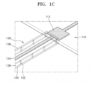
- FIG. IB illustrates a transmission line-integrated antenna utilizing a substrate integrated waveguide (SIW) structure which is applicable to mass production.
- FIG. IC is an enlarged view of the SIW structure of the transmission line-integrated antenna of FIG. IB.
- SIW substrate integrated waveguide
- FIG. 2 is a plan view of a transmission line-integrated patch antenna used in one embodiment of the present invention.
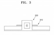
- FIG. 3 is a front view of a transmission line-integrated single-port patch antenna used in one embodiment of the present invention.
- the transmission line-integrated single-port patch antenna used in the embodiments of the present invention includes an antenna 110, 210, or 310 and a transmission line 120, 220, or 320 integrated with the antenna 110, 210, or 310.
- FIG. 4 illustrates a patch antenna as an example of the low-loss and flexible transmission line-integrated antenna for an mmWave band which is an element of the present invention.
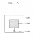
- FIG. 5 is a plan view of a patch antenna as an example of the low-loss and flexible transmission line-integrated single-port antenna for an mmWave band which is an element of the present invention.
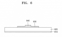
- FIG. 6 is a front view of the patch antenna.
- the patch antenna 110, 210, or 310 includes a ground plate 410 or 610, a dielectric substrate 420, 520, or 620, a signal conversion portion 430, 530, or 630, and an electricity feeding portion 440, 540, or 640.
- the ground plate 410 or 610 is located on a bottom surface of the patch antenna 110 or 210, performs a function of a ground, and includes a metal.
- the dielectric substrate 420, 520, or 620 is formed of a dielectric having a certain thickness on the ground plate 410 or 610.
- the signal conversion portion 430, 530, or 630 is formed on the dielectric substrate 420, 520, or 620 and converts an electrical signal of a mobile communication terminal into an electromagnetic wave signal and radiates the electromagnetic wave signal into the air or receives and converts an electromagnetic wave signal in the air into an electrical signal of a mobile communication terminal.
- the electricity feeding portion 440, 540, or 640 is formed on the dielectric substrate 420, 520, or 620 and is connected to the signal conversion portion 430, 530, or 630.
- FIG. 7 illustrates a flat cable type transmission line included in one embodiment of the low-loss and flexible transmission line-integrated antenna for an mmWave band which is an element of the present invention.
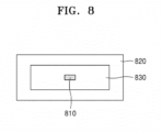
- FIG. 8 is a front view illustrating a transmission line (flat cable) included in one embodiment of the low-loss and flexible transmission line-integrated antenna for an mmWave band according to the present invention.
- the transmission line 120, 220, or 320 includes a central conductor 710 or 810, an external conductor 720 or 820, and a dielectric 730 or 830.
- the central conductor 710 or 810 is connected to the electricity feeding portion 440, 540, or 640 of the antenna 110, 210, or 310 and transmits, as a signal line, the transmitted or received electrical signal.
- the external conductor 720 or 820 has the same axis as that of the central conductor 710 or 810 and shields the central conductor 710 or 810 in an axial direction a-b of the central conductor 710 or 810.
- the dielectric 730 or 830 is formed between the central conductor and the external conductor in the axial direction.
- the dielectric substrate 420, 520, or 620 used in the antenna 110, 210, or 310 and the dielectric 730 or 830 used in the transmission line 120, 220, or 320 may have a sheet shape including a nanostructured material formed by electrospinning a resin in a variety of phases (solid, liquid, and gas) at a high voltage.
- the nanostructured material is used as a dielectric material included in the antenna and the transmission line in the low-loss and flexible transmission line-integrated antenna for an mmWave band which is an element of the present invention.
- the dielectric material is formed by selecting an adequate resin among resins in a variety of phases (solid, liquid, and gas) and electrospinning the resin at a certain high voltage and will be referred to as nanoflon hereinafter.
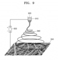
- FIG. 9 illustrates an example of an apparatus which manufactures nanoflon through electrospinning.
- a high voltage 930 is applied to a space between the injector 910 and a substrate on which spinning is performed, and the polymer solution flows thereinto at a certain speed, as electricity is applied to a liquid suspended from an end of a capillary due to surface tension, a nanosized thin thread 940 is formed, and as time passes, nanofibers 950 having a non-woven nanostructure are accumulated.
- a material formed of the accumulated nanofibers as described above is nanoflon.
- polycarbonate PC
- PU polyurethane
- PVDF polyvinylidene difluoride
- Nylon polyamide
- PAN polyacrylonitrile
- nanoflon Since nanoflon has low dielectric permittivity and a large amount of air, nanoflon may be used as a dielectric of a transmission line and a dielectric substrate of an antenna.
- a relative dielectric permittivity er of nanoflon used in the present invention is about I.56, and a dielectric loss tangent value Tan 8 is about 0.0008.
- the relative dielectric permittivity and dielectric loss tangent value of the nanoflon are significantly low.
- the transmission line-integrated antenna according to the present invention may be flexible and provide flexibility in an installation even in a small space of a smart phone by using a low-loss and flexible material.
- the dielectric used in FIGS. IA to 8 may be a nanostructured nanosheet dielectric formed by electrospinning a resin in a variety of phases at a high voltage. That is, the dielectric used herein is a low-loss nanosheet material including a lot of air layers between dielectrics which is formed by electrospinning a dielectric resin such as PC, PU, PVDF, polyethersulfone (PES), nylon, PAN, and the like at a high voltage instead of a material including only a dielectric material without an air layer in a dielectric such as existing polyimide (PI) and liquid crystal polymer (LCP)-based materials.
- PI polyimide
- LCP liquid crystal polymer
- a conductor included m a component of the low-loss and flexible transmission line-integrated antenna for an mmWave band shown in FIGS. IA to 8 may be formed using a variety of methods such as etching, printing, depositing, and the like. Also, the conductor and the nanosheet dielectric included in the low-loss and flexible transmission line-integrated antenna for an mmWave band shown in FIGS. IA to 8 include not only a single layer structure but also a multilayer structure in which a plurality of layers are repetitively stacked so as to transmit and receive a multiple signal at the same time.
- the conductor and the nanosheet dielectric may be connected using a bonding solution or a bonding sheet having a structure having a low relative dielectric permittivity and a low dielectric loss of a thin film layer.
- the low-loss and flexible transmission line-integrated single-port antenna used as an element of to the present invention includes a microstrip patch signal radiator, a variety of shapes of patch type antenna radiator structures, or a diagonal line type patch antenna structure.
- An antenna radiator patch may be located on an uppermost end surface, a nanosheet dielectric having a certain thickness may be formed on a bottom surface of the antenna radiator patch, and a ground plate formed of a metal may be formed on a lowermost end surface.
- a bonding force may be reinforced using a low-loss dielectric bonding sheet or a bonding solution and a conductor vapor-deposited on a nanosheet dielectric may be utilized.
- the transmission line 120 includes a nanosheet dielectric 126 having a certain thickness, conductors 128 and 129 formed on a top surface and a bottom surface of the nanosheet dielectric 126, and a stripline signal line 124 formed as a signal line in centers of the nanosheet dielectric 126 and the conductors 128 and 129.
- a plurality of via holes 122 may be formed between a surface of the conductor 128 formed above the nanosheet dielectric 126 and a surface of the conductor 129 formed below the nanosheet dielectric 126.
- the low-loss and flexible transmission line-integrated antenna may include a stripline structure in which the plurality of via holes 122 are formed along a longitudinal edge of the transmission line 120 in a direction parallel to the signal line 124.
- the stripline signal line 124 is directly connected to a radiator patch conductor 112 of the antenna.
- the plurality of via holes 122 are configured to prevent a leakage from the signal line and transmission/reception of noise and provides an excellent noise cut property with respect to a broadband including an mmWave band using an SIW structure.
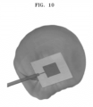
- FIG. 10 illustrates a beam pattern (radiation pattern) of a transmission line-integrated patch antenna as an example of the low-loss and flexible transmission line-integrated single-port antenna for an mmWave band used in the low-loss and flexible transmission line-integrated multi-port antenna according to the present invention.
- the beam pattern is an electric field strength of a radiated electromagnetic wave and indicates directivity as shown in FIG. 10 .
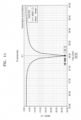
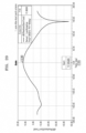
- FIG. 11 illustrates an input reflection parameter S11 according to a frequency of a transmission line-integrated patch antenna as an example of a low-loss and flexible transmission line-integrated antenna for an mmWave band used in a transmission line-integrated multi-port antenna according to the present invention.
- a value of S11 decreases and signal power input into the antenna is reflected, does not return, is maximally radiated outside through the antenna, has high radiation efficiency, and is well matched at a frequency of 28 GHz that is a 5G communication frequency.
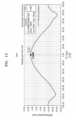
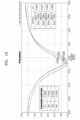
- FIG. 12 illustrates a gain property of a transmission line-integrated patch antenna as an example of the low-loss and flexible transmission line-integrated antenna for an mmWave band used in the transmission line-integrated multi-port antenna according to the present invention.
- a gain property of vertical polarization is about 6.6 dBi at 0 radian which is a very high antenna gain property.
- the low-loss and flexible transmission line-integrated single-port antenna for an mmWave band used in the embodiment of the present invention includes not only a patch antenna or a microstrip patch antenna but also an antenna and a transmission line using dielectrics.
- the antenna used as an element of the present invention may be formed in the form of a dipole antenna or a monopole antenna.
- the antenna is a built-in antenna built in a mobile communication terminal and may be applied to a planar inverted F antenna (PIFA).
- PIFA planar inverted F antenna
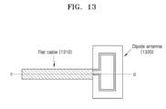
- FIG. 13 is a plan view of a transmission line-integrated dipole antenna as another example of the low-loss and flexible transmission line-integrated single-port antenna for an mmWave band used in the embodiment of the present invention.
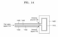
- FIG. 14 is an axial (c-d of FIG. 13 ) cross-sectional view of a transmission line-integrated dipole antenna as another example of a low-loss and flexible transmission line-integrated single-port antenna for an mmWave band used in an embodiment according to the present invention.
- the transmission line-integrated dipole antenna includes a flat cable 1310 that is a transmission line and a dipole antenna 1320 integrated with the flat cable 1310.
- the dipole antenna 1320 includes a dipole type signal conversion portion 1410 and a dielectric 1420
- the transmission line 1310 includes a central conductor 1440 which transmits a signal, an external conductor 1450, and a dielectric 1450 which is formed of a dielectric material having a low dielectric permittivity and a low loss between the central conductor and the external conductor.
- the transmission line-integrated dipole antenna usable in the embodiment of the present invention includes one end 15 connected to a signal line of the flat cable which is the transmission line 1310 and another end 16 connected to a ground line of the antenna.
- FIG. 15 illustrates an example of a mobile communication device in which the low-loss and flexible transmission line-integrated single-port antenna for an mmWave band used in the embodiment of the present invention is mounted;
- the mobile communication device includes a low-loss and flexible transmission line-integrated single-port antenna TLIA for an mmWave band according to the present invention which is connected to a circuit module of the mobile communication device, transmits and receives electrical signals, and externally radiates electromagnetic waves through an antenna.
- the low-loss and flexible curved transmission line-integrated multi-port antenna for an mmWave band which includes the above-described low-loss and flexible transmission line-integrated single-port antennas will be described.
- FIG. 16 illustrates one embodiment of the low-loss and flexible curved transmission line-integrated multi-port antenna for an mmWave band according to the present invention.
- FIG. 17 is a plan view illustrating one embodiment of the low-loss and flexible curved transmission line-integrated multi-port antenna for an mmWave band according to the present invention.
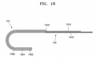
- FIG. 18 is a side view illustrating one embodiment of the low-loss and flexible curved transmission line-integrated multi-port antenna for an mmWave band according to the present invention.
- the low-loss and flexible curved transmission line-integrated multi-port antenna includes a multi-port antenna portion 160 and a transmission line portion 165.
- the multi-port antenna portion 160 includes a plurality of single antennas 1610, 1620, 1630, and 1640 and forms multi-ports, for example, four ports. Each of the single antennas forms one port.
- the transmission line portion 165 includes a plurality of transmission lines 1660, 1670, 1680, and 1690 which correspond to the single antennas 1610, 1620, 1630, and 1640, respectively, and have a curved shape.
- Central conductors 1662, 1762, 1862, and 1962 used as signal lines of the respective transmission lines are integrated with corresponding electricity feeding portions 1616, 1626, 1636, and 1646 of the single antennas, respectively.
- each of the plurality of antennas 1610, 1620, 1630, and 1640 includes a dielectric substrate 1612, 1622, 1632, 1642, 420, 520, or 620, a signal conversion portion 1614, 1624, 1634, 1644, 430, 530, or 630, and the electricity feeding portion 1616, 1626, 1636, 1646, 440, 540, or 640.
- the dielectric substrate 1612, 1622, 1632, 1642, 420, 520, or 620 is formed of a dielectric having a certain thickness on the ground plate 410 or 610.
- the signal conversion portion 1614, 1624, 1634, 430, 530, or 630 is formed on the dielectric substrate 1612, 1622, 1632, 1642, 420, 520, or 620 and converts an electrical signal of the mobile communication device into an electromagnetic wave signal and radiates the electromagnetic wave signal into the air or receives and converts an electromagnetic wave signal in the air into an electrical signal of a mobile communication device.
- the electricity feeding portion 1616, 1626, 1636, 1646, 440, 540, or 640 is formed on the dielectric substrate 1612, 1622, 1632, 1642, 420, 520, or 620) and connected to the signal conversion portion 1614, 1624, 1634, 1644, 430, 530, or 630.
- each of the plurality of transmission lines 1660, 1670, 1680, and 1690 includes the central conductor 1662, 1762, 1862, 1962, 710, or 810, external conductor 1666, 1766, 1866, 1966, 720 or 820, and the dielectric 1664, 1764, 1864, 1964, 730 or 830.
- One end of the central conductor 1662, 1762, 1862, 1962, 710 or 810 is integrated with the electricity feeding portion 1616, 1626, 1636, 1646, 440, 540, or 640 of the single antenna and transfers the transmitted or received electrical signal.
- the external conductor 1666, 1766, 1866, 1966, 720 or 820 has the same axis as that of the central conductor 1662, 1762, 1862, 1962, 710, or 810 and shields the central conductor 1662, 1762, 1862, 1962, 710, or 810 in an axial direction of the central conductor 1662, 1762, 1862, 1962, 710, or 810.
- the dielectric 1664, 1764, 1864, 1964, 730 or 830 is formed between the central conductor 1662, 1762, 1862, 1962, 710, or 810 and the external conductor 1666, 1766, 1866, 1966, 720 or 820 in the axial direction.
- the dielectric 1664, 1764, 1864, 1964, 730 or 830 may be a nanostructured sheet material formed by electrospinning a resin at a high voltage as described above with reference to FIG. 9 .
- a beam pattern (radiation pattern) of the plurality of single antennas 1610, 1620, 1630, and 1640 may include circular polarization.
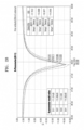
- FIG. 19 illustrates a property of an input reflection parameter S11 according to a frequency of one example of the low-loss and flexible curved transmission line-integrated multi-port antenna for an mmWave band according to the present invention.
- the transmission line-integrated multi-port patch antenna according to one embodiment of the present invention has excellent impedance and an excellent reflection parameter with respect to signal power input into the antenna at a frequency of 28 GHz which is a 5G communication frequency.
- FIG. 20 illustrates a gam property of one example of the low-loss and flexible curved transmission line-integrated multi-port antenna for an mmWave band according to the present invention.
- a gain property of vertical polarization is about 12.86 dBi at 0 radian which is a very high antenna gain property.
- the low-loss and flexible curved transmission line-integrated multi-port antenna for an mmWave band may be used while being mounted in a 5G mobile communication device.
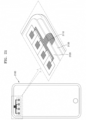
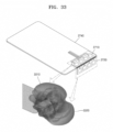
- FIG. 21 illustrates a mobile communication device in which a low-loss and flexible curved transmission line-integrated multi-port antenna for an mmWave band according to an embodiment of the present invention is mounted.
- FIG. 22 is a side view of the mobile communication device in which the low-loss and flexible curved transmission line-integrated multi-port antenna for an mmWave band according to the embodiment of the present invention is mounted.
- a curved lower surface 2112 of a transmission line is located above a printed circuit board (PCB) 2130 of a mobile communication device 2100 and an upper surface 2114 of the transmission line is located on an inner surface of a mobile communication device case 2120.
- PCB printed circuit board
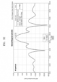
- FIG. 23 illustrates properties of input reflection parameters S11, S22, S33, and S44 according to a frequency of one example of the mobile communication device in which the low-loss and flexible curved transmission line-integrated multi-port antenna for an mmWave band according to the present invention is mounted.
- the transmission line-integrated multi-port patch antenna according to one embodiment of the present invention has excellent impedance and an excellent reflection parameter with respect to signal power input into the antenna on the basis of a frequency of 28 GHz which is a 5G communication frequency.
- FIG. 24 illustrates a gam property of one example of the mobile communication device in which the low-loss and flexible curved transmission line-integrated multi-port antenna for an mmWave band according to the present invention is mounted.
- the multi-port that is, all of four ports are turned ON, a gain property is about 13.56 dBi at 0 radian which is a very high antenna gain property.
- the four ports are shown as an example of the multi-port, the multi-port may include eight ports, sixteen ports, thirty-three ports, sixty-four ports, and the like, and the present invention is not limited to the number of ports.
- a low-loss and flexible curved transmission line-integrated multi-port antenna for an mmWave band may include a curved multi-port antenna portion and a transmission line portion.
- the multi-port antenna portion includes a plurality of single antennas and forms multi-ports, for example, four ports.
- Each of the single antennas has a curved shape and forms one port.
- the transmission line portion includes a plurality of transmission lines, and each of the transmission lines corresponds to each of the single antennas.
- a central conductor used as a signal line of each transmission line is integrated with an electricity feeding portion of the corresponding single antenna.
- each of the plurality of single antennas includes a dielectric substrate 420, 520, or 620, a signal conversion portion 430, 530, or 630, and an electricity feeding portion 440, 540, or 640.
- the dielectric substrate 420, 520, or 620 is formed of a dielectric having a certain thickness on the ground plate 410 or 610.
- the signal conversion portion 430, 530, or 630 is formed on the dielectric substrate 420, 520, or 620 and converts an electrical signal of a mobile communication terminal into an electromagnetic wave signal and radiates the electromagnetic wave signal into the air or receives and converts an electromagnetic wave signal in the air into an electrical signal of a mobile communication terminal.
- the electricity feeding portion 440, 540, or 640 is formed on the dielectric substrate 420, 520, or 620 and is connected to the signal conversion portion 430, 530, or 630.
- each of the plurality of transmission lines includes the central conductor 710 or 810, the external conductor 720 or 820, and the dielectric 730 or 830.
- the central conductor 710 or 810 is integrated with the electricity feeding portion 440, 540, or 640 and transfers the transmitted or received electrical signal.
- the external conductor 720 or 820 has the same axis as that of the central conductor 710 or 810 and shields the central conductor 710 or 810 m an axial direction of the central conductor 710 or 810.
- the dielectric 730 or 830 is formed between the central conductor 710 or 810 and the external conductor 720 or 820 in the axial direction.
- the dielectric 730 or 830 may be a nanostructured sheet material formed by electrospinning a resin at a high voltage as described above with reference to FIG. 9 .
- FIG. 25 illustrates on example of a mobile communication device in which a low-loss and flexible curved transmission line-integrated multi-port antenna for an mmWave band according to another embodiment of the present invention is mounted.
- a transmission line 2520 integrated with a four-port antenna 2510 of 28 GHz may be connected to a module 2530 of the mobile communication device. It is shown that a four-port antenna 2540 of 28 GHz may be mounted curvedly one an edge of the mobile communication device 2500.
- the low-loss and flexible orthogonal transmission line-integrated multi-port antenna for an mmWave band not forming part of the present invention which includes the above-described low-loss and flexible transmission line-integrated single-port antennas will be described.
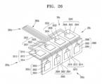
- FIG. 26 illustrates one example of the low-loss and flexible orthogonal transmission line-integrated multi-port antenna for an mmWave band according to the present invention.
- the low-loss and flexible orthogonal transmission line-integrated multi-port antenna for an mmWave band according to one example not forming part of the present invention includes a first multi-port antenna 26a and a second multi-port antenna 26b perpendicular to the first multi-port antenna 26a.
- the first multi-port antenna 26a includes a first multi-port antenna portion 260a and a first transmission line portion 260b.
- the first multi-port antenna portion 260a includes a plurality of single antennas 1610, 1620, 1630, and 1640, which are horizontally arranged, and forms multi-ports, for example, four ports. Each of the single antennas forms one port.
- the first transmission line portion 260b includes a plurality of transmission lines, and each of the transmission lines corresponds to a singles antenna 2610, 2620, 2630, or 2640 and is integrated with an electricity feeding portion 2616, 2626, 2636, or 2646 to which a central conductor used as a signal line of each transmission line corresponds.
- each of the plurality of antennas 2610, 2620, 2630, and 2640 includes a dielectric substrate 2614, 2624, 2634, 2644, 420, 520, or 620, a signal conversion portion 2612, 2622, 2632, 2642, 430, 530, or 630, and the electricity feeding portion 2616, 2626, 2636, 2646, 440, 540, or 640.
- the dielectric substrate 2614, 2624, 2634, 2644, 420, 520, or 620 is formed of a dielectric having a certain thickness on the ground plate 410 or 610.
- the signal conversion portion 2612, 2622, 2632, 2642, 430, 530, or 630 is formed on the dielectric substrate 2614, 2624, 2634, 2644, 420, 520, or 620 and converts an electrical signal of a mobile communication device into an electromagnetic wave signal and radiates the electromagnetic wave signal into the air or receives and converts an electromagnetic wave signal in the air into an electrical signal of a mobile communication device.
- the electricity feeding portion 2616, 2626, 2636, 2646, 440, 540, or 640 is formed on the dielectric substrate 2614, 2624, 2634, 2644, 420, 520, or 620) and connected to the signal conversion portion 2612, 2622, 2632, 2642,430, 530, or 630.
- each of the plurality of transmission lines includes the central conductor 710 or 810, the external conductor 720 or 820, and the dielectric 730 or 830.
- One end of the central conductor 710 or 810 is integrated with the electricity feeding portion 2616, 2626, 2636, 2646, 440, 540, or 640 and transfers the transmitted or received electrical signal.
- the external conductor 720 or 820 has the same axis as that of the central conductor 710 or 810 and shields the central conductor 710 or 810 in an axial direction of the central conductor 710 or 810.
- the dielectric 730 or 830 is formed between the central conductor 710 or 810 and the external conductor 720 or 820 in the axial direction.
- the dielectric 730 or 830 may be a nanostructured sheet material formed by electrospinning a resin at a high voltage as described above with reference to FIG. 9 .
- the second multi-port antenna 26a includes a second multi-port antenna portion 265a and a second transmission line portion 265b.
- the second multi-port antenna portion 265a includes a plurality of single antennas 2650, 2660 2670, and 2680, is disposed perpendicular to the first multi-port antenna portion 260a, and forms multi-ports, for example, four ports. Each of the single antennas forms one port.
- the second transmission line portion 265b includes a plurality of transmission lines, and each of the transmission lines corresponds to a singles antenna 2650, 2660, 2670, or 2680 and is integrated with an electricity feeding portion 2656, 2666, 2676, or 2686 to which a central conductor used as a signal line of each transmission line corresponds.
- each of the plurality of antennas 2650, 2660, 2670, and 2680 includes a dielectric substrate 2654, 2664, 2674, 2684, 420, 520, or 620, a signal conversion portion 2652, 2662, 2672, 2682, 430, 530, or 630, and the electricity feeding portion 2656, 2666, 2676, 2686, 440, 540, or 640.
- the dielectric substrate 2654, 2664, 2674, 2684, 420, 520, or 620 is formed of a dielectric having a certain thickness on the ground plate 410 or 610.
- the signal conversion portion 2652, 2662, 2672, 2682, 430, 530, or 630 is formed on the dielectric substrate 2654, 2664, 2674, 2684, 420, 520, or 620 and converts an electrical signal of a mobile communication device into an electromagnetic wave signal and radiates the electromagnetic wave signal into the air or receives and converts an electromagnetic wave signal in the air into an electrical signal of a mobile communication device.
- the electricity feeding portion 2656, 2666, 2676, 2686, 440, 540, or 640 is formed on the dielectric substrate 2654, 2664, 2674, 2684, 420, 520, or 620) and connected to the signal conversion portion 2652, 2662, 2672, 2682,430, 530, or 630.
- each of the plurality of transmission lines includes the central conductor 710 or 810, the external conductor 720 or 820, and the dielectric 730 or 830.
- the central conductor 710 or 810 is integrated with the electricity feeding portion 2656, 2666, 2676, 2686, 440, 540, or 640 and transfers the transmitted or received electrical signal.
- the external conductor 720 or 820 has the same axis as that of the central conductor 710 or 810 and shields the central conductor 710 or 810 in an axial direction of the central conductor 710 or 810.
- the dielectric 730 or 830 is formed between the central conductor 710 or 810 and the external conductor 720 or 820 in the axial direction.
- the dielectric 730 or 830 may be a nanostructured sheet material formed by electrospinning a resin at a high voltage as described above with reference to FIG. 9 .
- the first multi-port antenna 26a of the low-loss and flexible orthogonal transmission line-integrated multi-port antenna for an mmWave band not forming part of the present invention includes a plurality of such single antennas 2610, 2620, 2630, and 2640 horizontally arranged such that a beam pattern (radiation pattern) includes vertical polarization wave or horizontal polarization.
- the second multi-port antenna 26b thereof includes a plurality of such single antennas 2650, 2660, 2670, and 2680 vertically arranged such that a beam pattern (radiation pattern) includes vertical polarization wave or horizontal polarization.
- the beam pattern (radiation pattern) of the plurality of single antennas may include circular polarization.
- FIG. 27 illustrates a beam pattern (radiation pattern) 2730 of a transmission line-integrated patch antenna of a first multi-port antenna 2710 in the first multi-port antenna 2710 and a second multi-port antenna 2720 which are installed orthogonally in a mobile communication device 2740 as one example of the low-loss and flexible orthogonal transmission line-integrated multi-port antenna for an mmWave band used in the transmission line-integrated multi-port antenna.
- the beam pattern 2730 is an electric field strength of a radiated electromagnetic wave and indicates directivity as shown in FIG. 27 .
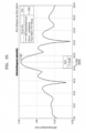
- FIG. 28 illustrates properties of input reflection parameters S11, S22, S33, and S44 according to a frequency of the first multi-port antenna 2710 of the low-loss and flexible orthogonal transmission line-integrated multi-port antenna for an mmWave band.
- the first multi-port antenna 2710 of the transmission line-integrated multi-port patch antenna has excellent impedance and an excellent reflection parameter with respect to signal power input into the antenna at a frequency of 28 GHz which is a 5G communication frequency.
- FIG. 29 illustrates a gain property of the first multi-port antenna 2710 of the low-loss and flexible orthogonal transmission line-integrated multi-port antenna for an mmWave band.
- a gain property of vertical polarization is about 12.29 dBi at 0 radian which is a very high antenna gain property.
- FIG. 30 illustrates a beam pattern (radiation pattern) 3030 of a transmission line-integrated patch antenna of the second multi-port antenna 2720 in the first multi-port antenna 2710 and the second multi-port antenna 2720 which are installed orthogonally in the mobile communication device 2740 as one embodiment of the low-loss and flexible orthogonal transmission line-integrated multi-port antenna for an mmWave band used in the transmission line-integrated multi-port antenna.
- the beam pattern 3030 is an electric field strength of a radiated electromagnetic wave and indicates directivity as shown in FIG. 30 .
- FIG. 31 illustrates properties of input reflection parameters S11, S22, S33, and S44 according to a frequency of the second multi-port antenna 2720 of the low-loss and flexible orthogonal transmission line-integrated multi-port antenna for an mmWave band not forming part of the present invention.
- the second multi-port antenna 2720 of the transmission line-integrated multi-port patch antenna has excellent impedance and an excellent reflection parameter with respect to signal power input into the antenna at a frequency of 28 GHz which is a 5G communication frequency.
- FIG. 32 illustrates a gain property of the second multi-port antenna 2720 of the low-loss and flexible orthogonal transmission line-integrated multi-port antenna for an mmWave band.
- a gain property of vertical polarization is about 12.79 dBi at 0 radian which is a very high antenna gain property.
- FIG. 33 illustrates beam patterns (radiation patterns) 3310 and 3320 of the transmission line-integrated patch antennas of the first multi-port antenna 2710 and the second multi-port antenna 2720 which are installed orthogonally in the mobile communication device 2740 as one embodiment of the low-loss and flexible orthogonal transmission line-integrated multi-port antenna for an mmWave band used in the transmission line-integrated multi-port antenna not forming part of the present invention.
- the beam patterns 3310 and 3320 are electric field strengths of radiated electromagnetic waves, and the beam pattern 3310 of the first multi-port antenna 2710 and the beam pattern 3320 of the second multi-port antenna 2720 are combined with each other and show respective directivities.
- FIG. 34 illustrates properties of input reflection parameters S11, S22, S33, S44, S55, S66, S77, and S88 according to a frequency of the first multi-port antenna 2710 and the second multi-port antenna 2720 which are included in the low-loss and flexible orthogonal transmission line-integrated multi-port antenna for an mmWave band.
- the first multi-port antenna 2710 and the second multi-port antenna 2720 included in the transmission line-integrated multi-port patch antenna have excellent impedances and excellent reflection parameters with respect to signal power input into the antenna at a frequency of 28 GHz which is a 5G communication frequency.
- FIG. 35 illustrates a gain property of the low-loss and flexible orthogonal transmission line-integrated multi-port antenna for an mmWave band.
- a gain property of vertical polarization is about 11.02 dBi at 0 radian which is a very high antenna gain property.
- FIG. 36 illustrates a mobile communication device in which a low-loss and flexible orthogonal transmission line-integrated multi-port antenna for an mmWave band not forming part of the present invention is mounted.
- eight multi-port antennas 3610 and 3620 are installed on each of horizontal and vertical edges of a mobile communication device 3630, and totally, sixteen ports are shown.
- the example is not limited to the number of ports.
- a low-loss and flexible curved transmission line-integrated multi-port antenna for an mmWave band may be used as an antenna for a high frequency band of several ten GHzs used in a smart phone of a next-generation 5G mobile communication system.
- the low-loss and flexible curved transmission line-integrated multi-port antenna uses a dielectric material having low relative dielectric permittivity and a low dielectric loss tangent value for dielectrics used in a transmission line and an antenna so as to transmit or radiate superhigh frequency signals at a less loss.
- a loss which may occur due to a connection portion between the transmission line and the antenna may be eliminated by integrating the transmission line with the antenna so as to reduce a loss of a signal in a superhigh frequency band.
- a mobile built-in antenna may be implemented using a flexible material having flexibility so as to locate the antenna at a position of minimizing an influence of surroundings in a mobile device such as a smart phone and the like and to more efficiently arrange components in a mobile communication device.
Landscapes
- Engineering & Computer Science (AREA)
- Computer Networks & Wireless Communication (AREA)
- Mechanical Engineering (AREA)
- Textile Engineering (AREA)
- Waveguide Aerials (AREA)
- Variable-Direction Aerials And Aerial Arrays (AREA)
- Waveguides (AREA)
- Details Of Aerials (AREA)
Claims (8)
- Verlustarme und flexible, gekrümmte übertragungsleitungsintegrierte Mehrfachanschlussantenne für ein Millimeterwellenband, umfassend:einen Mehrfachanschlussantennenabschnitt (160), der eine Vielzahl von Einzelantennen umfasst, die Mehrfachanschlüsse bilden, wobei jede der Einzelantennen einen Anschluss bildet; undeinen Übertragungsleitungsabschnitt (165), der eine Vielzahl von Übertragungsleitungen umfasst,wobei die Einzelantennen jeweils umfassen:eine Erdungsplatte (410, 610);ein dielektrisches Substrat (1612, 1622, 1632, 1642, 420, 520, 620), das aus einem Dielektrikum (730, 830) gebildet ist, das eine gewisse Dicke auf der Erdungsplatte aufweist;einen Signalumwandlungsabschnitt (1614, 1624, 1634, 1644, 430, 530, 630), der auf dem dielektrischen Substrat gebildet ist und konfiguriert ist, um ein elektrisches Signal eines mobilen Kommunikationsendgeräts in ein elektromagnetisches Wellensignal umzuwandeln und das elektromagnetische Wellensignal in die Luft abzustrahlen oder um ein elektromagnetisches Wellensignal in der Luft in ein elektrisches Signal eines mobilen Kommunikationsendgeräts zu empfangen; undeinen Stromzuführungsabschnitt (1616, 1626, 1636, 1646, 440, 540, 640), der auf dem dielektrischen Substrat gebildet und mit dem Signalumwandlungsabschnitt verbunden ist,wobei die Übertragungsleitungen jeweils umfassen:einen Mittelleiter (1662, 1762, 1862, 1962, 710, 810), der ein Ende aufweist, das mit dem Stromzuführungsabschnitt der Antenne integriert ist und konfiguriert ist, um das übertragene oder empfangene elektrische Signal zu übermitteln;einen Außenleiter (1666, 1766, 1866, 1966, 720, 820), der den Mittelleiter in einer axialen Richtung des Mittelleiters umgibt, um den Mittelleiter abzuschirmen; undein Nanoschicht-Dielektrikum (1664, 1764, 1864, 1964, 730, 830), das den zwischen dem Mittelleiter und dem Außenleiter gebildeten Raum in der axialen Richtung ausfüllt, undwobei das Nanoschicht-Dielektrikum aus einem verlustarmen Nanoschicht-Material besteht, das in einer Nanoschicht mit viel Luftraum durch Elektrospinnen eines Harzes bei hoher Spannung gebildet wird,wobei die Übertragungsleitungen (1660, 1670, 1680, 1690), die jeweils den Einzelantennen (1610, 1620, 1630, 1640) entsprechen, mit Elektrizitätszuführungsabschnitten (1616, 1626, 1636, 1646, 440, 540, 640) der Einzelantennen integriert sind, denen als Signalleitungen der Übertragungsleitungen verwendete Mittelleiter entsprechen, und der Übertragungsleitungsabschnitt (165) eine gekrümmte Form aufweist.
- Verlustarme und flexible, gekrümmte übertragungsleitungsintegrierte Mehrfachanschlussantenne nach Anspruch 1, wobei der Mehrfachanschlussantennenabschnitt (160) ein Strahlmuster (Strahlungsmuster) der Vielzahl von Einzelantennen umfasst, so dass das von der Vielzahl von Einzelantennen gesendete oder empfangene elektromagnetische Wellensignal zirkular polarisiert ist.
- Verlustarme und flexible, gekrümmte übertragungsleitungsintegrierte Mehrfachanschlussantenne nach Anspruch 1, wobei die Einzelantennen (1610, 1620, 1630, 1640) und die Übertragungsleitungen (165) gebildet werden, indem eine Bindungskraft zwischen dem Leiter und einer dielektrischen Schicht unter Verwendung einer verlustarmen Bindungsschicht oder Bindungslösung verstärkt wird oder der Leiter auf einer Nanoschicht abgeschieden wird.
- Verlustarme und flexible, gekrümmte übertragungsleitungsintegrierte Mehrfachanschlussantenne nach Anspruch 1, wobei die Übertragungsleitungen (165) jeweils umfassen:das Nanoschicht-Dielektrikum (126), das eine gewisse Dicke aufweist;Leiteroberflächen (128, 129), die auf einer oberen Oberfläche und einer unteren Oberfläche des Nanoschicht-Dielektrikums gebildet sind, undeine Streifenleitungsübertragungsleitung (124), die als Signalleitung in Zentren des Nanoschicht-Dielektrikums und der Leiteroberflächen ausgebildet ist, undwobei eine Vielzahl von Durchkontaktierungslöchern (122) zwischen der über dem Nanoschicht-Dielektrikum gebildeten Leiteroberfläche und der unter dem Nanoschicht-Dielektrikum gebildeten Leiteroberfläche ausgebildet ist.
- Verlustarme und flexible, gekrümmte übertragungsleitungsintegrierte Mehrfachanschlussantenne nach Anspruch 1, wobei die Einzelantennen (1610, 1620, 1630, 1640) jeweils eine Struktur einer Patch-Antenne, einer Mikrostreifen-Patch-Antenne oder einer Patch-Antenne vom Diagonalleitungstyp aufweisen, wobei der Signalumwandlungsabschnitt ein Patch ist,wobei die Patch-Antenne oder die Mikrostreifenantenne aus einem Metall gebildet ist und ferner eine Erdungsplatte umfasst, die sich auf einer Unterseite befindet, undwobei ein dielektrisches Substrat als ein Dielektrikum gebildet ist, das eine gewisse Dicke auf der Erdungsplatte aufweist.
- Verlustarme und flexible, gekrümmte übertragungsleitungsintegrierte Mehrfachanschlussantenne nach Anspruch 1, wobei die Einzelantenne eine Dipolantenne, eine Monopolantenne oder eine Schlitzantenne ist, die unter Verwendung einer Vielfalt an Schlitzen implementiert ist.
- Verlustarme und flexible, gekrümmte übertragungsleitungsintegrierte Mehrfachanschlussantenne nach Anspruch 1, wobei die Einzelantenne eine planare invertierte F-Antenne (PIFA) ist, die eine eingebaute Antenne ist, die in ein mobiles Kommunikationsendgerät eingebaut ist.
- Mobiles Kommunikationsendgerät, umfassend die verlustarme und flexible, gekrümmte übertragungsleitungsintegrierte Mehrfachanschlussantenne nach Anspruch einem der Ansprüche 1 bis 7.
Applications Claiming Priority (1)
| Application Number | Priority Date | Filing Date | Title |
|---|---|---|---|
| KR1020190014011A KR102091739B1 (ko) | 2019-02-01 | 2019-02-01 | 밀리미터파(mmWave) 대역용 전송선로 일체형 저손실 유연 곡면형 및 직각형 다중 포트 안테나 |
Publications (2)
| Publication Number | Publication Date |
|---|---|
| EP3691024A1 EP3691024A1 (de) | 2020-08-05 |
| EP3691024B1 true EP3691024B1 (de) | 2024-08-28 |
Family
ID=69400429
Family Applications (1)
| Application Number | Title | Priority Date | Filing Date |
|---|---|---|---|
| EP20154341.0A Active EP3691024B1 (de) | 2019-02-01 | 2020-01-29 | Verlustarme und flexible, gekrümmte oder orthogonale übertragungsleitungsintegrierte mehrfachanschlussantenne für millimeterwellenband |
Country Status (6)
| Country | Link |
|---|---|
| US (1) | US11309632B2 (de) |
| EP (1) | EP3691024B1 (de) |
| JP (1) | JP6955590B2 (de) |
| KR (1) | KR102091739B1 (de) |
| CN (1) | CN111525253B (de) |
| TW (1) | TWI725724B (de) |
Families Citing this family (14)
| Publication number | Priority date | Publication date | Assignee | Title |
|---|---|---|---|---|
| KR102057314B1 (ko) * | 2018-11-26 | 2020-01-22 | 주식회사 센서뷰 | 밀리미터파(mmWave) 대역용 전송선로 일체형 저손실 유연 다중 포트 안테나 |
| ES2953593T3 (es) | 2019-02-19 | 2023-11-14 | Samsung Electronics Co Ltd | Dispositivo electrónico que incluye una antena |
| KR102819076B1 (ko) * | 2020-04-02 | 2025-06-10 | 동우 화인켐 주식회사 | 안테나 패키지 및 이를 포함하는 화상 표시 장치 |
| KR102785360B1 (ko) * | 2020-08-28 | 2025-03-20 | 동우 화인켐 주식회사 | 회로 기판, 안테나 패키지 및 디스플레이 장치 |
| KR102906958B1 (ko) | 2020-09-24 | 2025-12-31 | 동우 화인켐 주식회사 | 안테나 패키지 및 이를 포함하는 화상 표시 장치 |
| CN112864585B (zh) * | 2021-01-22 | 2025-05-13 | 苏州硕贝德创新技术研究有限公司 | 一种应用于移动终端的5g毫米波通信模组 |
| KR20230063198A (ko) | 2021-11-01 | 2023-05-09 | 삼성전자주식회사 | 안테나 모듈을 포함하는 전자 장치 |
| WO2023171180A1 (ja) * | 2022-03-08 | 2023-09-14 | ソニーグループ株式会社 | 装置 |
| CN117791072A (zh) * | 2022-09-20 | 2024-03-29 | 华为技术有限公司 | 传输线、馈电网络及天线装置 |
| KR20240075498A (ko) | 2022-11-22 | 2024-05-29 | 주식회사 경우 | 고이득 특성을 갖는 슬롯 타입 안테나 |
| EP4730565A1 (de) * | 2023-06-30 | 2026-04-22 | Samsung Electronics Co., Ltd. | Elektronische vorrichtung mit antenne |
| TWI898654B (zh) * | 2023-07-13 | 2025-09-21 | 特崴光波導股份有限公司 | 天線模組與應用此天線模組之可攜式電子裝置 |
| CN116995402A (zh) * | 2023-08-30 | 2023-11-03 | 北京理工大学 | 一种基于MXene高电导率薄膜材料的柔性超薄微带贴片天线 |
| CN120280676A (zh) * | 2025-06-09 | 2025-07-08 | 四川海芯微科技有限公司 | 一种微带至共面波导馈电结构及其结构参数调试方法 |
Family Cites Families (20)
| Publication number | Priority date | Publication date | Assignee | Title |
|---|---|---|---|---|
| JPS5823403U (ja) * | 1981-08-04 | 1983-02-14 | 三菱電機株式会社 | 同軸導波管 |
| JPS6384053A (ja) * | 1986-09-29 | 1988-04-14 | Toshiba Corp | 同軸配線構造体 |
| JP3186018B2 (ja) * | 1995-07-27 | 2001-07-11 | 新光電気工業株式会社 | 高周波用配線基板 |
| JP2003208823A (ja) * | 2002-01-10 | 2003-07-25 | Fujikura Ltd | 高周波同軸ケーブル |
| JP2005051747A (ja) | 2003-07-14 | 2005-02-24 | Ngk Spark Plug Co Ltd | アンテナ装置およびその製造方法 |
| KR100714201B1 (ko) * | 2005-04-19 | 2007-05-02 | 한국정보통신대학교 산학협력단 | 초 광대역 안테나 |
| KR101195831B1 (ko) * | 2005-12-30 | 2012-11-05 | 엘지전자 주식회사 | 패치안테나 |
| EP1936741A1 (de) * | 2006-12-22 | 2008-06-25 | Sony Deutschland GmbH | Flexible substratintegrierte Wellenleiter |
| KR100955801B1 (ko) * | 2007-03-08 | 2010-05-06 | 주식회사 에이스테크놀로지 | 다중대역 내장형 안테나 |
| JP5770108B2 (ja) * | 2010-01-29 | 2015-08-26 | 株式会社東芝 | アンテナ部品とその製造方法 |
| KR101501057B1 (ko) * | 2012-06-04 | 2015-03-10 | 주식회사 아모그린텍 | 전자파 차폐시트, 그 제조방법 및 이를 구비한 내장형 안테나 |
| CN104505600B (zh) * | 2014-11-27 | 2017-04-26 | 国家电网公司 | 一种测量局部放电信号的开缝串联馈电微带天线阵 |
| CN107926117B (zh) * | 2015-08-21 | 2020-08-14 | 阿莫绿色技术有限公司 | 可穿戴柔性印刷电路板、其制造方法及利用其的可穿戴智能装置 |
| US10326205B2 (en) * | 2016-09-01 | 2019-06-18 | Wafer Llc | Multi-layered software defined antenna and method of manufacture |
| KR102744540B1 (ko) | 2016-12-30 | 2024-12-19 | 인텔 코포레이션 | 고주파수 통신 시스템들을 위한 분산된 스택형 안테나를 갖는 가요성 패키지 기판들로 설계된 마이크로전자 디바이스들 |
| JP6531786B2 (ja) * | 2017-06-13 | 2019-06-19 | Tdk株式会社 | アンテナ装置及びこれを備える回路基板 |
| CN110998974B (zh) * | 2017-07-31 | 2022-03-15 | 株式会社村田制作所 | 天线模块和通信装置 |
| CN108376828B (zh) * | 2018-01-25 | 2021-01-12 | 瑞声科技(南京)有限公司 | 天线系统及移动终端 |
| KR102057314B1 (ko) * | 2018-11-26 | 2020-01-22 | 주식회사 센서뷰 | 밀리미터파(mmWave) 대역용 전송선로 일체형 저손실 유연 다중 포트 안테나 |
| WO2020138448A1 (ja) * | 2018-12-28 | 2020-07-02 | 株式会社村田製作所 | 通信装置 |
-
2019
- 2019-02-01 KR KR1020190014011A patent/KR102091739B1/ko active Active
-
2020
- 2020-01-29 US US16/775,706 patent/US11309632B2/en active Active
- 2020-01-29 EP EP20154341.0A patent/EP3691024B1/de active Active
- 2020-01-31 JP JP2020015609A patent/JP6955590B2/ja active Active
- 2020-01-31 TW TW109103020A patent/TWI725724B/zh active
- 2020-02-03 CN CN202010078946.5A patent/CN111525253B/zh active Active
Also Published As
| Publication number | Publication date |
|---|---|
| JP6955590B2 (ja) | 2021-10-27 |
| CN111525253B (zh) | 2022-12-27 |
| EP3691024A1 (de) | 2020-08-05 |
| JP2020127196A (ja) | 2020-08-20 |
| US11309632B2 (en) | 2022-04-19 |
| CN111525253A (zh) | 2020-08-11 |
| US20200251825A1 (en) | 2020-08-06 |
| TWI725724B (zh) | 2021-04-21 |
| KR102091739B1 (ko) | 2020-03-20 |
| TW202046562A (zh) | 2020-12-16 |
Similar Documents
| Publication | Publication Date | Title |
|---|---|---|
| US11309632B2 (en) | Low-loss and flexible curved or orthogonal transmission line-integrated multi-port antenna for mmWave band | |
| US10978787B2 (en) | Low-loss and flexible transmission line-integrated multi-port antenna for mmWave band | |
| US10847890B2 (en) | Low-loss and flexible transmission line-integrated antenna for MMWave band | |
| US11545761B2 (en) | Dual-band cross-polarized 5G mm-wave phased array antenna | |
| JP6050967B2 (ja) | フェーズドアレイの広帯域連結リングアンテナ素子 | |
| EP3703185B1 (de) | Antenne | |
| EP3907823B1 (de) | Antenne | |
| EP2304844B1 (de) | Mikrostreifen-planargruppenantenne für satellitentelekommunikation, die für betrieb bei verschiedenen empfangs- und sendefrequenzen und mit kreuzpolarisationen ausgelegt ist | |
| CN114421154A (zh) | 双极化天线及移动传感器 | |
| CN119627415A (zh) | 一种天线及通信设备 | |
| CN204809416U (zh) | 天线装置 |
Legal Events
| Date | Code | Title | Description |
|---|---|---|---|
| PUAI | Public reference made under article 153(3) epc to a published international application that has entered the european phase |
Free format text: ORIGINAL CODE: 0009012 |
|
| STAA | Information on the status of an ep patent application or granted ep patent |
Free format text: STATUS: REQUEST FOR EXAMINATION WAS MADE |
|
| 17P | Request for examination filed |
Effective date: 20200129 |
|
| AK | Designated contracting states |
Kind code of ref document: A1 Designated state(s): AL AT BE BG CH CY CZ DE DK EE ES FI FR GB GR HR HU IE IS IT LI LT LU LV MC MK MT NL NO PL PT RO RS SE SI SK SM TR |
|
| AX | Request for extension of the european patent |
Extension state: BA ME |
|
| RAP3 | Party data changed (applicant data changed or rights of an application transferred) |
Owner name: SENSORVIEW CO., LTD. |
|
| RIN1 | Information on inventor provided before grant (corrected) |
Inventor name: YOO, HONG IL Inventor name: KIM, BYOUNG NAM |
|
| STAA | Information on the status of an ep patent application or granted ep patent |
Free format text: STATUS: EXAMINATION IS IN PROGRESS |
|
| 17Q | First examination report despatched |
Effective date: 20220725 |
|
| GRAP | Despatch of communication of intention to grant a patent |
Free format text: ORIGINAL CODE: EPIDOSNIGR1 |
|
| STAA | Information on the status of an ep patent application or granted ep patent |
Free format text: STATUS: GRANT OF PATENT IS INTENDED |
|
| INTG | Intention to grant announced |
Effective date: 20240321 |
|
| GRAS | Grant fee paid |
Free format text: ORIGINAL CODE: EPIDOSNIGR3 |
|
| GRAA | (expected) grant |
Free format text: ORIGINAL CODE: 0009210 |
|
| STAA | Information on the status of an ep patent application or granted ep patent |
Free format text: STATUS: THE PATENT HAS BEEN GRANTED |
|
| AK | Designated contracting states |
Kind code of ref document: B1 Designated state(s): AL AT BE BG CH CY CZ DE DK EE ES FI FR GB GR HR HU IE IS IT LI LT LU LV MC MK MT NL NO PL PT RO RS SE SI SK SM TR |
|
| REG | Reference to a national code |
Ref country code: CH Ref legal event code: EP |
|
| REG | Reference to a national code |
Ref country code: DE Ref legal event code: R096 Ref document number: 602020036489 Country of ref document: DE |
|
| REG | Reference to a national code |
Ref country code: IE Ref legal event code: FG4D |
|
| REG | Reference to a national code |
Ref country code: LT Ref legal event code: MG9D |
|
| PG25 | Lapsed in a contracting state [announced via postgrant information from national office to epo] |
Ref country code: NO Free format text: LAPSE BECAUSE OF FAILURE TO SUBMIT A TRANSLATION OF THE DESCRIPTION OR TO PAY THE FEE WITHIN THE PRESCRIBED TIME-LIMIT Effective date: 20241128 |
|
| REG | Reference to a national code |
Ref country code: AT Ref legal event code: MK05 Ref document number: 1719009 Country of ref document: AT Kind code of ref document: T Effective date: 20240828 |
|
| PG25 | Lapsed in a contracting state [announced via postgrant information from national office to epo] |
Ref country code: NL Free format text: LAPSE BECAUSE OF FAILURE TO SUBMIT A TRANSLATION OF THE DESCRIPTION OR TO PAY THE FEE WITHIN THE PRESCRIBED TIME-LIMIT Effective date: 20240828 Ref country code: PL Free format text: LAPSE BECAUSE OF FAILURE TO SUBMIT A TRANSLATION OF THE DESCRIPTION OR TO PAY THE FEE WITHIN THE PRESCRIBED TIME-LIMIT Effective date: 20240828 Ref country code: FI Free format text: LAPSE BECAUSE OF FAILURE TO SUBMIT A TRANSLATION OF THE DESCRIPTION OR TO PAY THE FEE WITHIN THE PRESCRIBED TIME-LIMIT Effective date: 20240828 Ref country code: GR Free format text: LAPSE BECAUSE OF FAILURE TO SUBMIT A TRANSLATION OF THE DESCRIPTION OR TO PAY THE FEE WITHIN THE PRESCRIBED TIME-LIMIT Effective date: 20241129 Ref country code: PT Free format text: LAPSE BECAUSE OF FAILURE TO SUBMIT A TRANSLATION OF THE DESCRIPTION OR TO PAY THE FEE WITHIN THE PRESCRIBED TIME-LIMIT Effective date: 20241230 |
|
| PG25 | Lapsed in a contracting state [announced via postgrant information from national office to epo] |
Ref country code: BG Free format text: LAPSE BECAUSE OF FAILURE TO SUBMIT A TRANSLATION OF THE DESCRIPTION OR TO PAY THE FEE WITHIN THE PRESCRIBED TIME-LIMIT Effective date: 20240828 |
|
| PG25 | Lapsed in a contracting state [announced via postgrant information from national office to epo] |
Ref country code: LV Free format text: LAPSE BECAUSE OF FAILURE TO SUBMIT A TRANSLATION OF THE DESCRIPTION OR TO PAY THE FEE WITHIN THE PRESCRIBED TIME-LIMIT Effective date: 20240828 |
|
| REG | Reference to a national code |
Ref country code: NL Ref legal event code: MP Effective date: 20240828 |
|
| PG25 | Lapsed in a contracting state [announced via postgrant information from national office to epo] |
Ref country code: IS Free format text: LAPSE BECAUSE OF FAILURE TO SUBMIT A TRANSLATION OF THE DESCRIPTION OR TO PAY THE FEE WITHIN THE PRESCRIBED TIME-LIMIT Effective date: 20241228 Ref country code: AT Free format text: LAPSE BECAUSE OF FAILURE TO SUBMIT A TRANSLATION OF THE DESCRIPTION OR TO PAY THE FEE WITHIN THE PRESCRIBED TIME-LIMIT Effective date: 20240828 |
|
| PG25 | Lapsed in a contracting state [announced via postgrant information from national office to epo] |
Ref country code: HR Free format text: LAPSE BECAUSE OF FAILURE TO SUBMIT A TRANSLATION OF THE DESCRIPTION OR TO PAY THE FEE WITHIN THE PRESCRIBED TIME-LIMIT Effective date: 20240828 |
|
| PG25 | Lapsed in a contracting state [announced via postgrant information from national office to epo] |
Ref country code: ES Free format text: LAPSE BECAUSE OF FAILURE TO SUBMIT A TRANSLATION OF THE DESCRIPTION OR TO PAY THE FEE WITHIN THE PRESCRIBED TIME-LIMIT Effective date: 20240828 Ref country code: RS Free format text: LAPSE BECAUSE OF FAILURE TO SUBMIT A TRANSLATION OF THE DESCRIPTION OR TO PAY THE FEE WITHIN THE PRESCRIBED TIME-LIMIT Effective date: 20241128 |
|
| PG25 | Lapsed in a contracting state [announced via postgrant information from national office to epo] |
Ref country code: RS Free format text: LAPSE BECAUSE OF FAILURE TO SUBMIT A TRANSLATION OF THE DESCRIPTION OR TO PAY THE FEE WITHIN THE PRESCRIBED TIME-LIMIT Effective date: 20241128 Ref country code: PT Free format text: LAPSE BECAUSE OF FAILURE TO SUBMIT A TRANSLATION OF THE DESCRIPTION OR TO PAY THE FEE WITHIN THE PRESCRIBED TIME-LIMIT Effective date: 20241230 Ref country code: PL Free format text: LAPSE BECAUSE OF FAILURE TO SUBMIT A TRANSLATION OF THE DESCRIPTION OR TO PAY THE FEE WITHIN THE PRESCRIBED TIME-LIMIT Effective date: 20240828 Ref country code: NO Free format text: LAPSE BECAUSE OF FAILURE TO SUBMIT A TRANSLATION OF THE DESCRIPTION OR TO PAY THE FEE WITHIN THE PRESCRIBED TIME-LIMIT Effective date: 20241128 Ref country code: NL Free format text: LAPSE BECAUSE OF FAILURE TO SUBMIT A TRANSLATION OF THE DESCRIPTION OR TO PAY THE FEE WITHIN THE PRESCRIBED TIME-LIMIT Effective date: 20240828 Ref country code: LV Free format text: LAPSE BECAUSE OF FAILURE TO SUBMIT A TRANSLATION OF THE DESCRIPTION OR TO PAY THE FEE WITHIN THE PRESCRIBED TIME-LIMIT Effective date: 20240828 Ref country code: IS Free format text: LAPSE BECAUSE OF FAILURE TO SUBMIT A TRANSLATION OF THE DESCRIPTION OR TO PAY THE FEE WITHIN THE PRESCRIBED TIME-LIMIT Effective date: 20241228 Ref country code: HR Free format text: LAPSE BECAUSE OF FAILURE TO SUBMIT A TRANSLATION OF THE DESCRIPTION OR TO PAY THE FEE WITHIN THE PRESCRIBED TIME-LIMIT Effective date: 20240828 Ref country code: GR Free format text: LAPSE BECAUSE OF FAILURE TO SUBMIT A TRANSLATION OF THE DESCRIPTION OR TO PAY THE FEE WITHIN THE PRESCRIBED TIME-LIMIT Effective date: 20241129 Ref country code: FI Free format text: LAPSE BECAUSE OF FAILURE TO SUBMIT A TRANSLATION OF THE DESCRIPTION OR TO PAY THE FEE WITHIN THE PRESCRIBED TIME-LIMIT Effective date: 20240828 Ref country code: ES Free format text: LAPSE BECAUSE OF FAILURE TO SUBMIT A TRANSLATION OF THE DESCRIPTION OR TO PAY THE FEE WITHIN THE PRESCRIBED TIME-LIMIT Effective date: 20240828 Ref country code: BG Free format text: LAPSE BECAUSE OF FAILURE TO SUBMIT A TRANSLATION OF THE DESCRIPTION OR TO PAY THE FEE WITHIN THE PRESCRIBED TIME-LIMIT Effective date: 20240828 Ref country code: AT Free format text: LAPSE BECAUSE OF FAILURE TO SUBMIT A TRANSLATION OF THE DESCRIPTION OR TO PAY THE FEE WITHIN THE PRESCRIBED TIME-LIMIT Effective date: 20240828 |
|
| PG25 | Lapsed in a contracting state [announced via postgrant information from national office to epo] |
Ref country code: SM Free format text: LAPSE BECAUSE OF FAILURE TO SUBMIT A TRANSLATION OF THE DESCRIPTION OR TO PAY THE FEE WITHIN THE PRESCRIBED TIME-LIMIT Effective date: 20240828 Ref country code: DK Free format text: LAPSE BECAUSE OF FAILURE TO SUBMIT A TRANSLATION OF THE DESCRIPTION OR TO PAY THE FEE WITHIN THE PRESCRIBED TIME-LIMIT Effective date: 20240828 Ref country code: RO Free format text: LAPSE BECAUSE OF FAILURE TO SUBMIT A TRANSLATION OF THE DESCRIPTION OR TO PAY THE FEE WITHIN THE PRESCRIBED TIME-LIMIT Effective date: 20240828 |
|
| PG25 | Lapsed in a contracting state [announced via postgrant information from national office to epo] |
Ref country code: EE Free format text: LAPSE BECAUSE OF FAILURE TO SUBMIT A TRANSLATION OF THE DESCRIPTION OR TO PAY THE FEE WITHIN THE PRESCRIBED TIME-LIMIT Effective date: 20240828 |
|
| PG25 | Lapsed in a contracting state [announced via postgrant information from national office to epo] |
Ref country code: CZ Free format text: LAPSE BECAUSE OF FAILURE TO SUBMIT A TRANSLATION OF THE DESCRIPTION OR TO PAY THE FEE WITHIN THE PRESCRIBED TIME-LIMIT Effective date: 20240828 |
|
| PG25 | Lapsed in a contracting state [announced via postgrant information from national office to epo] |
Ref country code: IT Free format text: LAPSE BECAUSE OF FAILURE TO SUBMIT A TRANSLATION OF THE DESCRIPTION OR TO PAY THE FEE WITHIN THE PRESCRIBED TIME-LIMIT Effective date: 20240828 Ref country code: SK Free format text: LAPSE BECAUSE OF FAILURE TO SUBMIT A TRANSLATION OF THE DESCRIPTION OR TO PAY THE FEE WITHIN THE PRESCRIBED TIME-LIMIT Effective date: 20240828 |
|
| REG | Reference to a national code |
Ref country code: DE Ref legal event code: R097 Ref document number: 602020036489 Country of ref document: DE |
|
| PLBE | No opposition filed within time limit |
Free format text: ORIGINAL CODE: 0009261 |
|
| STAA | Information on the status of an ep patent application or granted ep patent |
Free format text: STATUS: NO OPPOSITION FILED WITHIN TIME LIMIT |
|
| 26N | No opposition filed |
Effective date: 20250530 |
|
| REG | Reference to a national code |
Ref country code: CH Ref legal event code: PL |
|
| PG25 | Lapsed in a contracting state [announced via postgrant information from national office to epo] |
Ref country code: SE Free format text: LAPSE BECAUSE OF FAILURE TO SUBMIT A TRANSLATION OF THE DESCRIPTION OR TO PAY THE FEE WITHIN THE PRESCRIBED TIME-LIMIT Effective date: 20240828 |
|
| PG25 | Lapsed in a contracting state [announced via postgrant information from national office to epo] |
Ref country code: MC Free format text: LAPSE BECAUSE OF FAILURE TO SUBMIT A TRANSLATION OF THE DESCRIPTION OR TO PAY THE FEE WITHIN THE PRESCRIBED TIME-LIMIT Effective date: 20240828 Ref country code: LU Free format text: LAPSE BECAUSE OF NON-PAYMENT OF DUE FEES Effective date: 20250129 |
|
| GBPC | Gb: european patent ceased through non-payment of renewal fee |
Effective date: 20250129 |
|
| PG25 | Lapsed in a contracting state [announced via postgrant information from national office to epo] |
Ref country code: GB Free format text: LAPSE BECAUSE OF NON-PAYMENT OF DUE FEES Effective date: 20250129 Ref country code: BE Free format text: LAPSE BECAUSE OF NON-PAYMENT OF DUE FEES Effective date: 20250131 |
|
| PG25 | Lapsed in a contracting state [announced via postgrant information from national office to epo] |
Ref country code: FR Free format text: LAPSE BECAUSE OF NON-PAYMENT OF DUE FEES Effective date: 20250131 |
|
| PG25 | Lapsed in a contracting state [announced via postgrant information from national office to epo] |
Ref country code: CH Free format text: LAPSE BECAUSE OF NON-PAYMENT OF DUE FEES Effective date: 20250131 |
|
| REG | Reference to a national code |
Ref country code: BE Ref legal event code: MM Effective date: 20250131 |
|
| PG25 | Lapsed in a contracting state [announced via postgrant information from national office to epo] |
Ref country code: IE Free format text: LAPSE BECAUSE OF NON-PAYMENT OF DUE FEES Effective date: 20250129 |
|
| PGFP | Annual fee paid to national office [announced via postgrant information from national office to epo] |
Ref country code: DE Payment date: 20260217 Year of fee payment: 7 |
|
| PG25 | Lapsed in a contracting state [announced via postgrant information from national office to epo] |
Ref country code: CY Free format text: LAPSE BECAUSE OF FAILURE TO SUBMIT A TRANSLATION OF THE DESCRIPTION OR TO PAY THE FEE WITHIN THE PRESCRIBED TIME-LIMIT Effective date: 20240828 |
|
| PG25 | Lapsed in a contracting state [announced via postgrant information from national office to epo] |
Ref country code: TR Free format text: LAPSE BECAUSE OF FAILURE TO SUBMIT A TRANSLATION OF THE DESCRIPTION OR TO PAY THE FEE WITHIN THE PRESCRIBED TIME-LIMIT Effective date: 20240828 |
|
| PG25 | Lapsed in a contracting state [announced via postgrant information from national office to epo] |
Ref country code: LT Free format text: LAPSE BECAUSE OF FAILURE TO SUBMIT A TRANSLATION OF THE DESCRIPTION OR TO PAY THE FEE WITHIN THE PRESCRIBED TIME-LIMIT Effective date: 20240828 |