EP3675604A1 - Method for producing ceramic substrate, and ceramic substrate - Google Patents
Method for producing ceramic substrate, and ceramic substrate Download PDFInfo
- Publication number
- EP3675604A1 EP3675604A1 EP18848939.7A EP18848939A EP3675604A1 EP 3675604 A1 EP3675604 A1 EP 3675604A1 EP 18848939 A EP18848939 A EP 18848939A EP 3675604 A1 EP3675604 A1 EP 3675604A1
- Authority
- EP
- European Patent Office
- Prior art keywords
- electrode layer
- warpage
- ceramic substrate
- present
- controlling
- Prior art date
- Legal status (The legal status is an assumption and is not a legal conclusion. Google has not performed a legal analysis and makes no representation as to the accuracy of the status listed.)
- Granted
Links
Images


Classifications
-
- H—ELECTRICITY
- H05—ELECTRIC TECHNIQUES NOT OTHERWISE PROVIDED FOR
- H05K—PRINTED CIRCUITS; CASINGS OR CONSTRUCTIONAL DETAILS OF ELECTRIC APPARATUS; MANUFACTURE OF ASSEMBLAGES OF ELECTRICAL COMPONENTS
- H05K1/00—Printed circuits
- H05K1/02—Details
- H05K1/0271—Arrangements for reducing stress or warp in rigid printed circuit boards, e.g. caused by loads, vibrations or differences in thermal expansion
-
- H—ELECTRICITY
- H10—SEMICONDUCTOR DEVICES; ELECTRIC SOLID-STATE DEVICES NOT OTHERWISE PROVIDED FOR
- H10W—GENERIC PACKAGES, INTERCONNECTIONS, CONNECTORS OR OTHER CONSTRUCTIONAL DETAILS OF DEVICES COVERED BY CLASS H10
- H10W40/00—Arrangements for thermal protection or thermal control
- H10W40/01—Manufacture or treatment
- H10W40/03—Manufacture or treatment of arrangements for cooling
- H10W40/037—Assembling together parts thereof
-
- H—ELECTRICITY
- H05—ELECTRIC TECHNIQUES NOT OTHERWISE PROVIDED FOR
- H05K—PRINTED CIRCUITS; CASINGS OR CONSTRUCTIONAL DETAILS OF ELECTRIC APPARATUS; MANUFACTURE OF ASSEMBLAGES OF ELECTRICAL COMPONENTS
- H05K1/00—Printed circuits
- H05K1/02—Details
-
- H—ELECTRICITY
- H05—ELECTRIC TECHNIQUES NOT OTHERWISE PROVIDED FOR
- H05K—PRINTED CIRCUITS; CASINGS OR CONSTRUCTIONAL DETAILS OF ELECTRIC APPARATUS; MANUFACTURE OF ASSEMBLAGES OF ELECTRICAL COMPONENTS
- H05K1/00—Printed circuits
- H05K1/02—Details
- H05K1/03—Use of materials for the substrate
-
- H—ELECTRICITY
- H05—ELECTRIC TECHNIQUES NOT OTHERWISE PROVIDED FOR
- H05K—PRINTED CIRCUITS; CASINGS OR CONSTRUCTIONAL DETAILS OF ELECTRIC APPARATUS; MANUFACTURE OF ASSEMBLAGES OF ELECTRICAL COMPONENTS
- H05K1/00—Printed circuits
- H05K1/02—Details
- H05K1/03—Use of materials for the substrate
- H05K1/0306—Inorganic insulating substrates, e.g. ceramic, glass
-
- H—ELECTRICITY
- H05—ELECTRIC TECHNIQUES NOT OTHERWISE PROVIDED FOR
- H05K—PRINTED CIRCUITS; CASINGS OR CONSTRUCTIONAL DETAILS OF ELECTRIC APPARATUS; MANUFACTURE OF ASSEMBLAGES OF ELECTRICAL COMPONENTS
- H05K3/00—Apparatus or processes for manufacturing printed circuits
- H05K3/02—Apparatus or processes for manufacturing printed circuits in which the conductive material is applied to the surface of the insulating support and is thereafter removed from such areas of the surface which are not intended for current conducting or shielding
- H05K3/06—Apparatus or processes for manufacturing printed circuits in which the conductive material is applied to the surface of the insulating support and is thereafter removed from such areas of the surface which are not intended for current conducting or shielding the conductive material being removed chemically or electrolytically, e.g. by photo-etch process
-
- H—ELECTRICITY
- H10—SEMICONDUCTOR DEVICES; ELECTRIC SOLID-STATE DEVICES NOT OTHERWISE PROVIDED FOR
- H10N—ELECTRIC SOLID-STATE DEVICES NOT OTHERWISE PROVIDED FOR
- H10N30/00—Piezoelectric or electrostrictive devices
- H10N30/01—Manufacture or treatment
- H10N30/08—Shaping or machining of piezoelectric or electrostrictive bodies
- H10N30/082—Shaping or machining of piezoelectric or electrostrictive bodies by etching, e.g. lithography
-
- H—ELECTRICITY
- H10—SEMICONDUCTOR DEVICES; ELECTRIC SOLID-STATE DEVICES NOT OTHERWISE PROVIDED FOR
- H10W—GENERIC PACKAGES, INTERCONNECTIONS, CONNECTORS OR OTHER CONSTRUCTIONAL DETAILS OF DEVICES COVERED BY CLASS H10
- H10W40/00—Arrangements for thermal protection or thermal control
- H10W40/20—Arrangements for cooling
- H10W40/25—Arrangements for cooling characterised by their materials
- H10W40/255—Arrangements for cooling characterised by their materials having a laminate or multilayered structure, e.g. direct bond copper [DBC] ceramic substrates
-
- H—ELECTRICITY
- H05—ELECTRIC TECHNIQUES NOT OTHERWISE PROVIDED FOR
- H05K—PRINTED CIRCUITS; CASINGS OR CONSTRUCTIONAL DETAILS OF ELECTRIC APPARATUS; MANUFACTURE OF ASSEMBLAGES OF ELECTRICAL COMPONENTS
- H05K2201/00—Indexing scheme relating to printed circuits covered by H05K1/00
- H05K2201/03—Conductive materials
- H05K2201/0332—Structure of the conductor
- H05K2201/0335—Layered conductors or foils
- H05K2201/0355—Metal foils
-
- H—ELECTRICITY
- H05—ELECTRIC TECHNIQUES NOT OTHERWISE PROVIDED FOR
- H05K—PRINTED CIRCUITS; CASINGS OR CONSTRUCTIONAL DETAILS OF ELECTRIC APPARATUS; MANUFACTURE OF ASSEMBLAGES OF ELECTRICAL COMPONENTS
- H05K2203/00—Indexing scheme relating to apparatus or processes for manufacturing printed circuits covered by H05K3/00
- H05K2203/03—Metal processing
- H05K2203/0353—Making conductive layer thin, e.g. by etching
-
- H—ELECTRICITY
- H05—ELECTRIC TECHNIQUES NOT OTHERWISE PROVIDED FOR
- H05K—PRINTED CIRCUITS; CASINGS OR CONSTRUCTIONAL DETAILS OF ELECTRIC APPARATUS; MANUFACTURE OF ASSEMBLAGES OF ELECTRICAL COMPONENTS
- H05K3/00—Apparatus or processes for manufacturing printed circuits
- H05K3/02—Apparatus or processes for manufacturing printed circuits in which the conductive material is applied to the surface of the insulating support and is thereafter removed from such areas of the surface which are not intended for current conducting or shielding
- H05K3/022—Processes for manufacturing precursors of printed circuits, i.e. copper-clad substrates
Definitions
- the present invention relates to a method of producing a ceramic substrate. More particularly, the present invention relates to a method of producing a ceramic substrate by controlling warpage of the ceramic substrate, and to a ceramic substrate produced thereby.
- a ceramic substrate is formed by integrally attaching a metal foil such as a copper foil to a ceramic base material.
- the ceramic substrate is manufactured through manufacturing processes such as active metal brazing (AMB), direct bond copper (DBC), and the like and may be classified into a ceramic AMB substrate, a ceramic DBC substrate, and the like depending on the manufacturing process.
- AMB active metal brazing
- DBC direct bond copper
- manufacturing of the ceramic DBC substrate involves directly bonding an oxidizable metal to a ceramic base material
- manufacturing of the ceramic AMB substrate involves brazing an active metal to a ceramic base material to form a layer and brazing metal to a brazing layer.
- a metal layer is formed, followed by a photolithography process, and then a pattern layer is formed by etching.
- the metal layers may differ from each other in area or thickness depending on the arrangement of patterns on the opposite surfaces.
- a phenomenon called "warpage” occurs in which a substrate warps toward one of the opposite surfaces under a high temperature environment.
- a substrate may warp under a high temperature environment.
- a case where the volume of the metal layer 3 formed on the lower surface is larger is referred to as a negative warpage, and this negative warpage is more likely to occur than a positive warpage, which is the opposite case.
- the present invention relates to a method of controlling the degree of warpage of a substrate as shown in below FIG. 1 .
- an objective of the present invention is to provide a method of producing a ceramic substrate by controlling warpage which may occur due to the difference in volume taken up by metal layers on opposite surfaces of a base material, thereby reducing the defect rate of the ceramic substrate, and to provide a ceramic substrate.
- a method of producing a ceramic substrate according to one aspect of the present invention includes: joining a metal layer to each of opposite surfaces of a ceramic base material; forming, on the metal layers, a first electrode layer and a second electrode layer having a larger volume than the first electrode layer; calculating the volumes of the first and second electrode layers; and controlling a thickness of the second electrode layer, thereby controlling warpage which may occur due to a difference between the volumes of the first and second electrode layers.
- controlling the warpage may be performed when a volume ratio of the first electrode layer to the second electrode layer is equal to or greater than 75% to less than 85%.
- controlling the warpage may be performed by controlling the thickness of the second electrode layer such that a volume ratio of the first electrode layer to the second electrode layer after performing the controlling the warpage is 95% ( ⁇ 10%).
- the method may further include determining that a failure has occurred when a volume ratio of the first electrode layer to the second electrode layer is less than 75%.
- the thickness of the second electrode layer may be controlled by etching.
- the present invention also provides a ceramic substrate produced by the above method.
- a method of producing a ceramic substrate according to the present invention through control of warpage by eliminating the difference in volume of metal layers formed on opposite surfaces of the ceramic substrate, it is possible to produce a ceramic substrate without warpage under a high temperature environment.
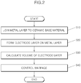
- FIG. 2 is a flowchart showing a method of producing a ceramic substrate according to the present invention
- FIG. 3 is a view showing an example of a ceramic substrate produced by the present invention.
- a method of producing a ceramic substrate, and a ceramic substrate according to embodiments of the present invention will be described with reference to FIGS. 2 and 3 .
- the method of producing the ceramic substrate according to the present invention is characterized by producing a ceramic substrate without causing warpage which may occur due to the difference in volume between metal layers such as copper foils joined to opposite surfaces of a ceramic base material, thereby preventing the substrate from warping toward one of the opposite surfaces.
- a metal layer made of copper (Cu) foil is joined to each of opposite surfaces (upper and lower surfaces) of a ceramic base material 10 (S10).
- the joining of the metal layer may be implemented by an active metal brazing (AMB) method or direct bond copper (DBC) method to form a ceramic substrate.
- the formation of the electrode layer is implemented by a photolithography process including photoresist application, masking, and exposure, and by an etching process.
- a first electrode layer 20 is formed on one surface of the opposite surfaces and a second electrode layer 30 is formed on the other surface such that the second electrode layer 30 is larger in volume than the first electrode layer 20.
- the volume of each of the electrode layers on the opposite surfaces having a volume difference as such is calculated through the product of the area and the thickness (S30).
- the warpage is controlled by controlling the thickness of the second electrode layer 30 (S40).
- This control is performed in such a manner that the volume of the first electrode layer/the volume of the second electrode layer ⁇ 100% is calculated and a warpage control is performed when a volume ratio that results from calculation is in a range of equal to or greater than 75% to less than 85%.
- the warpage is expected to occur at a degree of warpage of at least 0.3%, whereby the warpage control can be performed.
- volume ratio when the volume ratio is greater than 85%, it is determined to be within a normal range, and when the volume ratio is less than 75%, it is determined that a failure has occurred due to excessive warpage.
- the present invention may further include determining that a failure has occurred when the volume ratio is less than 75% as a result of calculation in S30.
- the case where the first electrode layer defines the upper surface of the ceramic base material and the volume ratio of the first electrode layer/the second electrode layer is less than 85% corresponds to a negative warpage
- the case where the first electrode layer defines the lower surface and the volume ratio of the first electrode layer/the second electrode layer is less than 85% corresponds to a positive warpage
- the warpage control of S40 is characterized by controlling the thickness of the second electrode layer 30 having a relatively large volume by soft etching.
- the present invention can obtain a final volume ratio of the first electrode layer/the second electrode layer of 95%.
- FIG. 3 is a view showing an example of a ceramic substrate produced by the above process.
- a ceramic base material 10 has a thickness of 320 ⁇ m .
- a first electrode layer 20 defines an upper surface of the ceramic base material and a second electrode layer 30 defines a lower surface.
- the area of the first electrode layer 20 is 5,179,2920 mm 2
- the area of the second electrode layer 30 is 6,055.3600 mm 2
- the thickness of the first electrode layer 20 and the second electrode layer 30 is 500 ⁇ m and the volume ratio of the first electrode layer 20/the second electrode layer 30 ⁇ 100% is approximately 83%, in which case the negative warpage is expected to occur.
- the thickness of the second electrode layer 30 was controlled by etching according to the present invention such that the volume ratio of the first electrode layer 20/the second electrode layer 30 ⁇ 100% was 95%. As a result, it was possible to produce a ceramic substrate subjected to additional soft etching at a thickness of 45 ⁇ m.
- the volume of the first electrode layer 20 is 2,589.646 mm 3
- the volume of the second electrode layer 30 is 2,755.188 mm 3 , resulting in a volume ratio of the first electrode layer 20/the second electrode layer 30 ⁇ 100% being 94%, whereby the warpage of the ceramic substrate can be controlled.
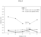
- FIG. 4 A result of comparing the occurrence of warpage between the ceramic substrate according to the present invention produced as described above with ceramic substrates having a volume ratio of 83% without warpage control is shown in FIG. 4 , and results of comparison are summarized in Table 1.
- Table 1 No. Electrode volume ratio Average flatness (mm) Variation (mm) Notes 1 83% 0.063 - room temperature warpage 2 83% 0.470 0.39 after reflow at 350°C 3 94% 0.110 0.04 after reflow at 350°C
- results of five samples are shown. As shown, it was found that in the case of 83% volume ratio without warpage control, the average flatness was 0.063 mm at room temperature (R.T). It was further found that in the case of 83% volume ratio without warpage control, the average flatness was 0.470 mm, indicating a significant change occurred.
- the average flatness was 0.110 mm, which was a very small value.
Landscapes
- Engineering & Computer Science (AREA)
- Microelectronics & Electronic Packaging (AREA)
- Manufacturing & Machinery (AREA)
- Chemical & Material Sciences (AREA)
- Ceramic Engineering (AREA)
- Inorganic Chemistry (AREA)
- Manufacturing Of Printed Wiring (AREA)
- Ceramic Products (AREA)
- Parts Printed On Printed Circuit Boards (AREA)
Abstract
Description
- The present invention relates to a method of producing a ceramic substrate. More particularly, the present invention relates to a method of producing a ceramic substrate by controlling warpage of the ceramic substrate, and to a ceramic substrate produced thereby.
- As well known in the art, a ceramic substrate is formed by integrally attaching a metal foil such as a copper foil to a ceramic base material. The ceramic substrate is manufactured through manufacturing processes such as active metal brazing (AMB), direct bond copper (DBC), and the like and may be classified into a ceramic AMB substrate, a ceramic DBC substrate, and the like depending on the manufacturing process.
- While manufacturing of the ceramic DBC substrate involves directly bonding an oxidizable metal to a ceramic base material, manufacturing of the ceramic AMB substrate involves brazing an active metal to a ceramic base material to form a layer and brazing metal to a brazing layer.
- In both processes, a metal layer is formed, followed by a photolithography process, and then a pattern layer is formed by etching.
- However, in forming metal layers on opposite surfaces of a ceramic base material, the metal layers may differ from each other in area or thickness depending on the arrangement of patterns on the opposite surfaces. When the difference in the area or thickness is greater than a certain ratio, a phenomenon called "warpage" occurs in which a substrate warps toward one of the opposite surfaces under a high temperature environment.
- As a result, when the degree of warpage is greater than 0.3%, the substrate is inevitably discarded as a defective product. The incidence rate of which accounts for a relatively large portion of the total production, causing a problem of continuous production loss.
- According to empirical data, when the volume ratio between the opposite metal layers reached the range of 75 to 85%, the degree of warpage was greater than 0.3%.
- As in an example of
FIG. 1 , when the volume ratio between ametal layer 2 formed on an upper surface of a base material 1 and ametal layer 3 formed on a lower surface of the base material is out of an appropriate range, a substrate may warp under a high temperature environment. As shown, a case where the volume of themetal layer 3 formed on the lower surface is larger is referred to as a negative warpage, and this negative warpage is more likely to occur than a positive warpage, which is the opposite case. - This may be solved by increasing the thickness of the base material. However, this approach is economically limited, and it is common for the base material to maintain a thickness ratio of approximately 1:1 with the metal layers.
- The present invention relates to a method of controlling the degree of warpage of a substrate as shown in below
FIG. 1 . - The above information disclosed in this Background section is only for enhancement of understanding of the background of the invention and therefore it may contain information that does not form the prior art that is already known to a person of ordinary skill in the art.
- Accordingly, the present invention has been made keeping in mind the above problems occurring in the related art, and an objective of the present invention is to provide a method of producing a ceramic substrate by controlling warpage which may occur due to the difference in volume taken up by metal layers on opposite surfaces of a base material, thereby reducing the defect rate of the ceramic substrate, and to provide a ceramic substrate.
- A method of producing a ceramic substrate according to one aspect of the present invention includes: joining a metal layer to each of opposite surfaces of a ceramic base material; forming, on the metal layers, a first electrode layer and a second electrode layer having a larger volume than the first electrode layer; calculating the volumes of the first and second electrode layers; and controlling a thickness of the second electrode layer, thereby controlling warpage which may occur due to a difference between the volumes of the first and second electrode layers.
- Furthermore, the controlling the warpage may be performed when a volume ratio of the first electrode layer to the second electrode layer is equal to or greater than 75% to less than 85%.
- Furthermore, the controlling the warpage may be performed by controlling the thickness of the second electrode layer such that a volume ratio of the first electrode layer to the second electrode layer after performing the controlling the warpage is 95% (± 10%).
- The method may further include determining that a failure has occurred when a volume ratio of the first electrode layer to the second electrode layer is less than 75%.
- Furthermore, the thickness of the second electrode layer may be controlled by etching.
- The present invention also provides a ceramic substrate produced by the above method.
- According to a method of producing a ceramic substrate according to the present invention, through control of warpage by eliminating the difference in volume of metal layers formed on opposite surfaces of the ceramic substrate, it is possible to produce a ceramic substrate without warpage under a high temperature environment.
- This can result a reduced defect rate of the substrate, thereby improving processability and productivity.
-
-
FIG. 1 is a view showing a concept of the present invention. -
FIG. 2 is a flowchart showing a method of producing a ceramic substrate according to the present invention. -
FIG. 3 is a view showing an example of a ceramic substrate produced by the present invention. -
FIG. 4 is a view showing a change in occurrence of warpage of the ceramic substrate according to the present invention. - The attached drawings illustrating exemplary embodiments of the present invention and the contents describing the attached drawings should be referred to so as to gain a sufficient understanding of the present invention, advantages in the operations of the present invention, and the objectives that are achieved by the implementation of the present invention.
- In the following description, it is to be noted that, when the functions of conventional elements and the detailed description of elements related with the present invention may make the gist of the present invention unclear, a detailed description of those elements will be omitted.
-
FIG. 2 is a flowchart showing a method of producing a ceramic substrate according to the present invention, andFIG. 3 is a view showing an example of a ceramic substrate produced by the present invention. Hereinafter, a method of producing a ceramic substrate, and a ceramic substrate according to embodiments of the present invention will be described with reference toFIGS. 2 and3 . - The method of producing the ceramic substrate according to the present invention is characterized by producing a ceramic substrate without causing warpage which may occur due to the difference in volume between metal layers such as copper foils joined to opposite surfaces of a ceramic base material, thereby preventing the substrate from warping toward one of the opposite surfaces.
- First, a metal layer made of copper (Cu) foil is joined to each of opposite surfaces (upper and lower surfaces) of a ceramic base material 10 (S10). The joining of the metal layer may be implemented by an active metal brazing (AMB) method or direct bond copper (DBC) method to form a ceramic substrate.
- Thereafter, an electrode layer is formed on each of the metal layers (S20).
- The formation of the electrode layer is implemented by a photolithography process including photoresist application, masking, and exposure, and by an etching process.
- Herein, a
first electrode layer 20 is formed on one surface of the opposite surfaces and asecond electrode layer 30 is formed on the other surface such that thesecond electrode layer 30 is larger in volume than thefirst electrode layer 20. - The volume of each of the electrode layers on the opposite surfaces having a volume difference as such is calculated through the product of the area and the thickness (S30).
- Thereafter, the warpage is controlled by controlling the thickness of the second electrode layer 30 (S40).
- This control is performed in such a manner that the volume of the first electrode layer/the volume of the second electrode layer × 100% is calculated and a warpage control is performed when a volume ratio that results from calculation is in a range of equal to or greater than 75% to less than 85%.
- According to the present invention, when the volume ratio of the first electrode layer to the = second electrode layer falls within this range, the warpage is expected to occur at a degree of warpage of at least 0.3%, whereby the warpage control can be performed.
- It is preferable that according to experimental values, when the volume ratio is greater than 85%, it is determined to be within a normal range, and when the volume ratio is less than 75%, it is determined that a failure has occurred due to excessive warpage.
- Therefore, the present invention may further include determining that a failure has occurred when the volume ratio is less than 75% as a result of calculation in S30.
- Herein, the case where the first electrode layer defines the upper surface of the ceramic base material and the volume ratio of the first electrode layer/the second electrode layer is less than 85% corresponds to a negative warpage, and the case where the first electrode layer defines the lower surface and the volume ratio of the first electrode layer/the second electrode layer is less than 85% (in this case, the volume ratio of the second electrode layer/the first electrode layer is greater than 115%) corresponds to a positive warpage.
- Further, the warpage control of S40 is characterized by controlling the thickness of the
second electrode layer 30 having a relatively large volume by soft etching. - Through the controlling of the thickness of the second electrode layer as such, the present invention can obtain a final volume ratio of the first electrode layer/the second electrode layer of 95%.
- Tolerance due to actual warpage control etching will occur. As a result, when the volume ratio of the first electrode layer/the second electrode layer is in a range of 85 to 105% corresponding to 95% ± 10%, the normal range in which substrate warpage is acceptable is fulfilled, whereby a substrate can be produced.
-
FIG. 3 is a view showing an example of a ceramic substrate produced by the above process. - A
ceramic base material 10 has a thickness of 320 µm. In an example, afirst electrode layer 20 defines an upper surface of the ceramic base material and asecond electrode layer 30 defines a lower surface. - In an example, the area of the
first electrode layer 20 is 5,179,2920 mm2, and the area of thesecond electrode layer 30 is 6,055.3600 mm2. In the absence of the warpage control of the present invention, the thickness of thefirst electrode layer 20 and thesecond electrode layer 30 is 500 µm and the volume ratio of thefirst electrode layer 20/thesecond electrode layer 30 × 100% is approximately 83%, in which case the negative warpage is expected to occur. - In this regard, the thickness of the
second electrode layer 30 was controlled by etching according to the present invention such that the volume ratio of thefirst electrode layer 20/thesecond electrode layer 30 × 100% was 95%. As a result, it was possible to produce a ceramic substrate subjected to additional soft etching at a thickness of 45 µm. - As a result of the warpage control, the volume of the
first electrode layer 20 is 2,589.646 mm3, and the volume of thesecond electrode layer 30 is 2,755.188 mm3, resulting in a volume ratio of thefirst electrode layer 20/thesecond electrode layer 30 × 100% being 94%, whereby the warpage of the ceramic substrate can be controlled. - A result of comparing the occurrence of warpage between the ceramic substrate according to the present invention produced as described above with ceramic substrates having a volume ratio of 83% without warpage control is shown in
FIG. 4 , and results of comparison are summarized in Table 1.Table 1 No. Electrode volume ratio Average flatness (mm) Variation (mm) Notes 1 83% 0.063 - room temperature warpage 2 83% 0.470 0.39 after reflow at 350° C 3 94% 0.110 0.04 after reflow at 350°C - Results of five samples are shown. As shown, it was found that in the case of 83% volume ratio without warpage control, the average flatness was 0.063 mm at room temperature (R.T). It was further found that in the case of 83% volume ratio without warpage control, the average flatness was 0.470 mm, indicating a significant change occurred.
- However, it was found that in the case of the substrate subjected to the warpage control according to the present invention, the average flatness was 0.110 mm, which was a very small value.
- It was further found that in the case of the substrate subjected to the warpage control according to the present invention, the variation after reflow at 350°C by soldering was 0.04 mm, which was a very small value.
- Although the present invention has been described above with reference to the exemplary drawings, the present invention is not limited to only the exemplary embodiments set forth herein and it will be understood by those skilled in the art that various changes and modifications may be made therein without departing from the spirit and scope of the present invention. Therefore, such changes and modifications should belong to the claims of the present invention, and the scope of the present invention should be determined on the basis of the appended claims.
-
- 10 :
- ceramic base material
- 20 :
- first electrode layer
- 30 :
- second electrode layer
- S10 :
- join metal layer to ceramic base material
- S20 :
- form electrode layer on metal layer
- S30 :
- calculate volume of electrode layer
- S40 :
- control warpage
Claims (6)
- A method of producing a ceramic substrate, the method comprising:joining a metal layer to each of opposite surfaces of a ceramic base material;forming, on the metal layers, a first electrode layer and a second electrode layer having a larger volume than the first electrode layer;calculating the volumes of the first and second electrode layers; andcontrolling a thickness of the second electrode layer, thereby controlling warpage which may occur due to a difference between the volumes of the first and second electrode layers.
- The method of claim 1, wherein the controlling the warpage is performed when a volume ratio of the first electrode layer to the second electrode layer is equal to or greater than 75% to less than 85%.
- The method of claim 1, wherein the controlling the warpage is performed by controlling the thickness of the second electrode layer such that a volume ratio of the first electrode layer to the second electrode layer after performing the controlling the warpage is 95% (± 10%).
- The method of claim 1, further comprising:
determining that a failure has occurred when a volume ratio of the first electrode layer to the second electrode layer is less than 75%. - The method of claim 1, wherein the thickness of the second electrode layer is controlled by etching.
- A ceramic substrate produced by the method of any one of claims 1 to 5.
Applications Claiming Priority (2)
| Application Number | Priority Date | Filing Date | Title |
|---|---|---|---|
| KR20170107002 | 2017-08-24 | ||
| PCT/KR2018/009722 WO2019039883A1 (en) | 2017-08-24 | 2018-08-23 | Method for producing ceramic substrate, and ceramic substrate |
Publications (3)
| Publication Number | Publication Date |
|---|---|
| EP3675604A1 true EP3675604A1 (en) | 2020-07-01 |
| EP3675604A4 EP3675604A4 (en) | 2020-10-07 |
| EP3675604B1 EP3675604B1 (en) | 2023-02-22 |
Family
ID=65761682
Family Applications (1)
| Application Number | Title | Priority Date | Filing Date |
|---|---|---|---|
| EP18848939.7A Active EP3675604B1 (en) | 2017-08-24 | 2018-08-23 | Method for producing ceramic substrate, and ceramic substrate |
Country Status (5)
| Country | Link |
|---|---|
| US (1) | US11355355B2 (en) |
| EP (1) | EP3675604B1 (en) |
| KR (2) | KR20190022383A (en) |
| CN (1) | CN110945971B (en) |
| WO (1) | WO2019039883A1 (en) |
Families Citing this family (6)
| Publication number | Priority date | Publication date | Assignee | Title |
|---|---|---|---|---|
| KR20200127511A (en) * | 2019-05-02 | 2020-11-11 | 주식회사 아모센스 | Ceramic substrate and manufacturing method for the same |
| WO2021095843A1 (en) * | 2019-11-15 | 2021-05-20 | デンカ株式会社 | Ceramic substrate, composite substrate, circuit board, method for producing ceramic substrate, method for producing composite substrate, method for producing circuit board, and method for producing plurality of circuit boards |
| US11582866B1 (en) * | 2021-07-22 | 2023-02-14 | Toyota Motor Engineering & Manufacturing North America, Inc. | Systems including a power device-embedded PCB directly joined with a cooling assembly and method of forming the same |
| CN114927494A (en) * | 2022-04-27 | 2022-08-19 | 蔚来动力科技(合肥)有限公司 | Packaging structure of double-sided heat dissipation module and electric automobile comprising same |
| CN116504683B (en) * | 2023-06-25 | 2023-08-25 | 江苏富乐华半导体科技股份有限公司 | A Warpage Control Method for Yin-Yang Copper DBC Products |
| WO2026009571A1 (en) * | 2024-07-05 | 2026-01-08 | 株式会社村田製作所 | Ceramic multilayer substrate and rfid tag |
Family Cites Families (14)
| Publication number | Priority date | Publication date | Assignee | Title |
|---|---|---|---|---|
| JPH0786703A (en) * | 1993-09-10 | 1995-03-31 | Toshiba Corp | Ceramics circuit board |
| GB2287131A (en) * | 1994-02-24 | 1995-09-06 | Plessey Semiconductors Ltd | Direct copper bonded substrates |
| JP4839461B2 (en) * | 2001-02-23 | 2011-12-21 | Dowaメタルテック株式会社 | Method for manufacturing aluminum oxide circuit board |
| JP4969738B2 (en) * | 2001-06-28 | 2012-07-04 | 株式会社東芝 | Ceramic circuit board and semiconductor module using the same |
| JP4692708B2 (en) | 2002-03-15 | 2011-06-01 | Dowaメタルテック株式会社 | Ceramic circuit board and power module |
| JP2004207587A (en) | 2002-12-26 | 2004-07-22 | Dowa Mining Co Ltd | Metal-ceramic bonding substrate and method of manufacturing the same |
| KR100731604B1 (en) | 2006-06-16 | 2007-06-22 | 삼성전기주식회사 | Method of manufacturing printed circuit board with enhanced stiffness characteristics |
| JP2008235852A (en) | 2007-02-23 | 2008-10-02 | Hitachi Metals Ltd | Ceramic substrate and semiconductor module using the same |
| KR100999918B1 (en) * | 2008-09-08 | 2010-12-13 | 삼성전기주식회사 | Printed Circuit Board and Manufacturing Method Thereof |
| KR101053141B1 (en) | 2009-06-08 | 2011-08-02 | 서울과학기술대학교 산학협력단 | Dummy pattern design method to suppress warpage of printed circuit board |
| JP5047315B2 (en) * | 2010-01-26 | 2012-10-10 | 株式会社東芝 | Ceramic circuit board |
| EP2624451B1 (en) * | 2010-09-28 | 2017-06-07 | Murata Manufacturing Co., Ltd. | Method for manufacturing piezoelectric device |
| JP5821389B2 (en) * | 2011-04-20 | 2015-11-24 | 三菱マテリアル株式会社 | Power module substrate manufacturing method and power module substrate |
| EP2727898B1 (en) * | 2011-06-30 | 2017-02-01 | Hitachi Metals, Ltd. | Brazing filler metal, brazing filler metal paste, ceramic circuit substrate, and ceramic master circuit substrate |
-
2018
- 2018-08-23 EP EP18848939.7A patent/EP3675604B1/en active Active
- 2018-08-23 KR KR1020180098396A patent/KR20190022383A/en not_active Ceased
- 2018-08-23 CN CN201880048669.4A patent/CN110945971B/en active Active
- 2018-08-23 WO PCT/KR2018/009722 patent/WO2019039883A1/en not_active Ceased
- 2018-08-23 US US16/630,073 patent/US11355355B2/en active Active
-
2024
- 2024-06-12 KR KR1020240076321A patent/KR20240093428A/en not_active Ceased
Also Published As
| Publication number | Publication date |
|---|---|
| US20200357660A1 (en) | 2020-11-12 |
| CN110945971B (en) | 2023-09-26 |
| KR20240093428A (en) | 2024-06-24 |
| US11355355B2 (en) | 2022-06-07 |
| CN110945971A (en) | 2020-03-31 |
| EP3675604A4 (en) | 2020-10-07 |
| WO2019039883A1 (en) | 2019-02-28 |
| EP3675604B1 (en) | 2023-02-22 |
| KR20190022383A (en) | 2019-03-06 |
Similar Documents
| Publication | Publication Date | Title |
|---|---|---|
| EP3675604B1 (en) | Method for producing ceramic substrate, and ceramic substrate | |
| KR20200127511A (en) | Ceramic substrate and manufacturing method for the same | |
| JP5287976B2 (en) | Resin wiring board | |
| US20220030708A1 (en) | Bonded substrate and manufacturing method of bonded substrate | |
| JP2019165083A (en) | Ceramic electronic component and method for manufacturing the same | |
| KR101089959B1 (en) | Printed circuit board and manufacturing method thereof | |
| EP2640172A1 (en) | Method for forming circuit on flexible laminate substrate | |
| EP3761351B1 (en) | Insulated circuit board | |
| EP3315303A1 (en) | Laminate substrate, conductive substrate, method for manufacturing laminate substrate and method for manufacturing conductive substrate | |
| JP2010050415A (en) | Substrate for power module and method of manufacturing the same | |
| KR20200122884A (en) | Method for manufacturing a ceramic substrate and the ceramic substrate made thereby | |
| US20170243799A1 (en) | Substrate for integrated circuit package | |
| CN109496065B (en) | A method of making an impedance | |
| KR20140072409A (en) | Method for processing a flexible cupper clad laminated film | |
| CN210491346U (en) | Control structure for improving asymmetric pressing circuit board warping | |
| CN106486426A (en) | Metal-ceramic plate for welding chip and the thereon method of welding chip | |
| KR20110045953A (en) | Flexible Copper Clad Laminated Film for Printed Circuit Board and Manufacturing Method Thereof | |
| JP2005347642A (en) | Manufacture of laminated ceramic electronic component | |
| JP2007234749A (en) | Manufacturing method of chip-shape solid electrolytic capacitor | |
| JP4761757B2 (en) | Manufacturing method of sealing material | |
| JP2006210489A (en) | Lead frame for semiconductor device and manufacturing method thereof | |
| JP2009010162A (en) | Method of manufacturing solid electrolytic capacitor | |
| KR20150071923A (en) | Flexible cupper clad laminated film for semi-additive and manufacturing method the same | |
| CN105101640B (en) | A kind of processing method of polytetrafluoroethylene (PTFE) step groove circuit board | |
| JP6212482B2 (en) | Copper base circuit board |
Legal Events
| Date | Code | Title | Description |
|---|---|---|---|
| STAA | Information on the status of an ep patent application or granted ep patent |
Free format text: STATUS: THE INTERNATIONAL PUBLICATION HAS BEEN MADE |
|
| PUAI | Public reference made under article 153(3) epc to a published international application that has entered the european phase |
Free format text: ORIGINAL CODE: 0009012 |
|
| STAA | Information on the status of an ep patent application or granted ep patent |
Free format text: STATUS: REQUEST FOR EXAMINATION WAS MADE |
|
| 17P | Request for examination filed |
Effective date: 20200115 |
|
| AK | Designated contracting states |
Kind code of ref document: A1 Designated state(s): AL AT BE BG CH CY CZ DE DK EE ES FI FR GB GR HR HU IE IS IT LI LT LU LV MC MK MT NL NO PL PT RO RS SE SI SK SM TR |
|
| AX | Request for extension of the european patent |
Extension state: BA ME |
|
| RIN1 | Information on inventor provided before grant (corrected) |
Inventor name: LEE, JI-HYUNG Inventor name: CHO, HYEON-CHOON Inventor name: PARK, IK-SEONG |
|
| A4 | Supplementary search report drawn up and despatched |
Effective date: 20200908 |
|
| RIC1 | Information provided on ipc code assigned before grant |
Ipc: H01L 23/00 20060101ALI20200904BHEP Ipc: H05K 1/02 20060101AFI20200904BHEP Ipc: H05K 3/02 20060101ALI20200904BHEP Ipc: H05K 3/06 20060101ALI20200904BHEP Ipc: H05K 1/03 20060101ALI20200904BHEP |
|
| DAV | Request for validation of the european patent (deleted) | ||
| DAX | Request for extension of the european patent (deleted) | ||
| INTG | Intention to grant announced |
Effective date: 20220927 |
|
| GRAS | Grant fee paid |
Free format text: ORIGINAL CODE: EPIDOSNIGR3 |
|
| STAA | Information on the status of an ep patent application or granted ep patent |
Free format text: STATUS: GRANT OF PATENT IS INTENDED |
|
| GRAA | (expected) grant |
Free format text: ORIGINAL CODE: 0009210 |
|
| STAA | Information on the status of an ep patent application or granted ep patent |
Free format text: STATUS: THE PATENT HAS BEEN GRANTED |
|
| AK | Designated contracting states |
Kind code of ref document: B1 Designated state(s): AL AT BE BG CH CY CZ DE DK EE ES FI FR GB GR HR HU IE IS IT LI LT LU LV MC MK MT NL NO PL PT RO RS SE SI SK SM TR |
|
| REG | Reference to a national code |
Ref country code: GB Ref legal event code: FG4D |
|
| REG | Reference to a national code |
Ref country code: CH Ref legal event code: EP |
|
| REG | Reference to a national code |
Ref country code: AT Ref legal event code: REF Ref document number: 1550342 Country of ref document: AT Kind code of ref document: T Effective date: 20230315 Ref country code: IE Ref legal event code: FG4D |
|
| REG | Reference to a national code |
Ref country code: DE Ref legal event code: R096 Ref document number: 602018046517 Country of ref document: DE |
|
| REG | Reference to a national code |
Ref country code: LT Ref legal event code: MG9D |
|
| REG | Reference to a national code |
Ref country code: NL Ref legal event code: MP Effective date: 20230222 |
|
| REG | Reference to a national code |
Ref country code: AT Ref legal event code: MK05 Ref document number: 1550342 Country of ref document: AT Kind code of ref document: T Effective date: 20230222 |
|
| PG25 | Lapsed in a contracting state [announced via postgrant information from national office to epo] |
Ref country code: RS Free format text: LAPSE BECAUSE OF FAILURE TO SUBMIT A TRANSLATION OF THE DESCRIPTION OR TO PAY THE FEE WITHIN THE PRESCRIBED TIME-LIMIT Effective date: 20230222 Ref country code: PT Free format text: LAPSE BECAUSE OF FAILURE TO SUBMIT A TRANSLATION OF THE DESCRIPTION OR TO PAY THE FEE WITHIN THE PRESCRIBED TIME-LIMIT Effective date: 20230622 Ref country code: NO Free format text: LAPSE BECAUSE OF FAILURE TO SUBMIT A TRANSLATION OF THE DESCRIPTION OR TO PAY THE FEE WITHIN THE PRESCRIBED TIME-LIMIT Effective date: 20230522 Ref country code: NL Free format text: LAPSE BECAUSE OF FAILURE TO SUBMIT A TRANSLATION OF THE DESCRIPTION OR TO PAY THE FEE WITHIN THE PRESCRIBED TIME-LIMIT Effective date: 20230222 Ref country code: LV Free format text: LAPSE BECAUSE OF FAILURE TO SUBMIT A TRANSLATION OF THE DESCRIPTION OR TO PAY THE FEE WITHIN THE PRESCRIBED TIME-LIMIT Effective date: 20230222 Ref country code: LT Free format text: LAPSE BECAUSE OF FAILURE TO SUBMIT A TRANSLATION OF THE DESCRIPTION OR TO PAY THE FEE WITHIN THE PRESCRIBED TIME-LIMIT Effective date: 20230222 Ref country code: HR Free format text: LAPSE BECAUSE OF FAILURE TO SUBMIT A TRANSLATION OF THE DESCRIPTION OR TO PAY THE FEE WITHIN THE PRESCRIBED TIME-LIMIT Effective date: 20230222 Ref country code: ES Free format text: LAPSE BECAUSE OF FAILURE TO SUBMIT A TRANSLATION OF THE DESCRIPTION OR TO PAY THE FEE WITHIN THE PRESCRIBED TIME-LIMIT Effective date: 20230222 Ref country code: AT Free format text: LAPSE BECAUSE OF FAILURE TO SUBMIT A TRANSLATION OF THE DESCRIPTION OR TO PAY THE FEE WITHIN THE PRESCRIBED TIME-LIMIT Effective date: 20230222 |
|
| PG25 | Lapsed in a contracting state [announced via postgrant information from national office to epo] |
Ref country code: SE Free format text: LAPSE BECAUSE OF FAILURE TO SUBMIT A TRANSLATION OF THE DESCRIPTION OR TO PAY THE FEE WITHIN THE PRESCRIBED TIME-LIMIT Effective date: 20230222 Ref country code: PL Free format text: LAPSE BECAUSE OF FAILURE TO SUBMIT A TRANSLATION OF THE DESCRIPTION OR TO PAY THE FEE WITHIN THE PRESCRIBED TIME-LIMIT Effective date: 20230222 Ref country code: IS Free format text: LAPSE BECAUSE OF FAILURE TO SUBMIT A TRANSLATION OF THE DESCRIPTION OR TO PAY THE FEE WITHIN THE PRESCRIBED TIME-LIMIT Effective date: 20230622 Ref country code: GR Free format text: LAPSE BECAUSE OF FAILURE TO SUBMIT A TRANSLATION OF THE DESCRIPTION OR TO PAY THE FEE WITHIN THE PRESCRIBED TIME-LIMIT Effective date: 20230523 Ref country code: FI Free format text: LAPSE BECAUSE OF FAILURE TO SUBMIT A TRANSLATION OF THE DESCRIPTION OR TO PAY THE FEE WITHIN THE PRESCRIBED TIME-LIMIT Effective date: 20230222 |
|
| PG25 | Lapsed in a contracting state [announced via postgrant information from national office to epo] |
Ref country code: SM Free format text: LAPSE BECAUSE OF FAILURE TO SUBMIT A TRANSLATION OF THE DESCRIPTION OR TO PAY THE FEE WITHIN THE PRESCRIBED TIME-LIMIT Effective date: 20230222 Ref country code: RO Free format text: LAPSE BECAUSE OF FAILURE TO SUBMIT A TRANSLATION OF THE DESCRIPTION OR TO PAY THE FEE WITHIN THE PRESCRIBED TIME-LIMIT Effective date: 20230222 Ref country code: EE Free format text: LAPSE BECAUSE OF FAILURE TO SUBMIT A TRANSLATION OF THE DESCRIPTION OR TO PAY THE FEE WITHIN THE PRESCRIBED TIME-LIMIT Effective date: 20230222 Ref country code: DK Free format text: LAPSE BECAUSE OF FAILURE TO SUBMIT A TRANSLATION OF THE DESCRIPTION OR TO PAY THE FEE WITHIN THE PRESCRIBED TIME-LIMIT Effective date: 20230222 Ref country code: CZ Free format text: LAPSE BECAUSE OF FAILURE TO SUBMIT A TRANSLATION OF THE DESCRIPTION OR TO PAY THE FEE WITHIN THE PRESCRIBED TIME-LIMIT Effective date: 20230222 |
|
| REG | Reference to a national code |
Ref country code: DE Ref legal event code: R097 Ref document number: 602018046517 Country of ref document: DE |
|
| PG25 | Lapsed in a contracting state [announced via postgrant information from national office to epo] |
Ref country code: SK Free format text: LAPSE BECAUSE OF FAILURE TO SUBMIT A TRANSLATION OF THE DESCRIPTION OR TO PAY THE FEE WITHIN THE PRESCRIBED TIME-LIMIT Effective date: 20230222 |
|
| PLBE | No opposition filed within time limit |
Free format text: ORIGINAL CODE: 0009261 |
|
| STAA | Information on the status of an ep patent application or granted ep patent |
Free format text: STATUS: NO OPPOSITION FILED WITHIN TIME LIMIT |
|
| 26N | No opposition filed |
Effective date: 20231123 |
|
| PG25 | Lapsed in a contracting state [announced via postgrant information from national office to epo] |
Ref country code: SI Free format text: LAPSE BECAUSE OF FAILURE TO SUBMIT A TRANSLATION OF THE DESCRIPTION OR TO PAY THE FEE WITHIN THE PRESCRIBED TIME-LIMIT Effective date: 20230222 |
|
| PG25 | Lapsed in a contracting state [announced via postgrant information from national office to epo] |
Ref country code: MC Free format text: LAPSE BECAUSE OF FAILURE TO SUBMIT A TRANSLATION OF THE DESCRIPTION OR TO PAY THE FEE WITHIN THE PRESCRIBED TIME-LIMIT Effective date: 20230222 |
|
| REG | Reference to a national code |
Ref country code: CH Ref legal event code: PL |
|
| PG25 | Lapsed in a contracting state [announced via postgrant information from national office to epo] |
Ref country code: MC Free format text: LAPSE BECAUSE OF FAILURE TO SUBMIT A TRANSLATION OF THE DESCRIPTION OR TO PAY THE FEE WITHIN THE PRESCRIBED TIME-LIMIT Effective date: 20230222 |
|
| PG25 | Lapsed in a contracting state [announced via postgrant information from national office to epo] |
Ref country code: LU Free format text: LAPSE BECAUSE OF NON-PAYMENT OF DUE FEES Effective date: 20230823 |
|
| PG25 | Lapsed in a contracting state [announced via postgrant information from national office to epo] |
Ref country code: LU Free format text: LAPSE BECAUSE OF NON-PAYMENT OF DUE FEES Effective date: 20230823 Ref country code: CH Free format text: LAPSE BECAUSE OF NON-PAYMENT OF DUE FEES Effective date: 20230831 |
|
| REG | Reference to a national code |
Ref country code: BE Ref legal event code: MM Effective date: 20230831 |
|
| REG | Reference to a national code |
Ref country code: IE Ref legal event code: MM4A |
|
| PG25 | Lapsed in a contracting state [announced via postgrant information from national office to epo] |
Ref country code: IT Free format text: LAPSE BECAUSE OF FAILURE TO SUBMIT A TRANSLATION OF THE DESCRIPTION OR TO PAY THE FEE WITHIN THE PRESCRIBED TIME-LIMIT Effective date: 20230222 |
|
| PG25 | Lapsed in a contracting state [announced via postgrant information from national office to epo] |
Ref country code: IE Free format text: LAPSE BECAUSE OF NON-PAYMENT OF DUE FEES Effective date: 20230823 |
|
| PG25 | Lapsed in a contracting state [announced via postgrant information from national office to epo] |
Ref country code: IE Free format text: LAPSE BECAUSE OF NON-PAYMENT OF DUE FEES Effective date: 20230823 |
|
| PG25 | Lapsed in a contracting state [announced via postgrant information from national office to epo] |
Ref country code: BE Free format text: LAPSE BECAUSE OF NON-PAYMENT OF DUE FEES Effective date: 20230831 |
|
| PG25 | Lapsed in a contracting state [announced via postgrant information from national office to epo] |
Ref country code: BG Free format text: LAPSE BECAUSE OF FAILURE TO SUBMIT A TRANSLATION OF THE DESCRIPTION OR TO PAY THE FEE WITHIN THE PRESCRIBED TIME-LIMIT Effective date: 20230222 |
|
| PG25 | Lapsed in a contracting state [announced via postgrant information from national office to epo] |
Ref country code: BG Free format text: LAPSE BECAUSE OF FAILURE TO SUBMIT A TRANSLATION OF THE DESCRIPTION OR TO PAY THE FEE WITHIN THE PRESCRIBED TIME-LIMIT Effective date: 20230222 |
|
| PG25 | Lapsed in a contracting state [announced via postgrant information from national office to epo] |
Ref country code: CY Free format text: LAPSE BECAUSE OF FAILURE TO SUBMIT A TRANSLATION OF THE DESCRIPTION OR TO PAY THE FEE WITHIN THE PRESCRIBED TIME-LIMIT; INVALID AB INITIO Effective date: 20180823 |
|
| PG25 | Lapsed in a contracting state [announced via postgrant information from national office to epo] |
Ref country code: HU Free format text: LAPSE BECAUSE OF FAILURE TO SUBMIT A TRANSLATION OF THE DESCRIPTION OR TO PAY THE FEE WITHIN THE PRESCRIBED TIME-LIMIT; INVALID AB INITIO Effective date: 20180823 |
|
| PGFP | Annual fee paid to national office [announced via postgrant information from national office to epo] |
Ref country code: DE Payment date: 20250721 Year of fee payment: 8 |
|
| PGFP | Annual fee paid to national office [announced via postgrant information from national office to epo] |
Ref country code: GB Payment date: 20250722 Year of fee payment: 8 |
|
| PGFP | Annual fee paid to national office [announced via postgrant information from national office to epo] |
Ref country code: FR Payment date: 20250725 Year of fee payment: 8 |
|
| PG25 | Lapsed in a contracting state [announced via postgrant information from national office to epo] |
Ref country code: TR Free format text: LAPSE BECAUSE OF FAILURE TO SUBMIT A TRANSLATION OF THE DESCRIPTION OR TO PAY THE FEE WITHIN THE PRESCRIBED TIME-LIMIT Effective date: 20230222 |