JP5522263B2 - Piezoelectric device and method for manufacturing piezoelectric device - Google Patents
Piezoelectric device and method for manufacturing piezoelectric device Download PDFInfo
- Publication number
- JP5522263B2 JP5522263B2 JP2012536502A JP2012536502A JP5522263B2 JP 5522263 B2 JP5522263 B2 JP 5522263B2 JP 2012536502 A JP2012536502 A JP 2012536502A JP 2012536502 A JP2012536502 A JP 2012536502A JP 5522263 B2 JP5522263 B2 JP 5522263B2
- Authority
- JP
- Japan
- Prior art keywords
- piezoelectric
- single crystal
- thin film
- support
- piezoelectric single
- Prior art date
- Legal status (The legal status is an assumption and is not a legal conclusion. Google has not performed a legal analysis and makes no representation as to the accuracy of the status listed.)
- Active
Links
- 238000004519 manufacturing process Methods 0.000 title claims description 78
- 238000000034 method Methods 0.000 title claims description 44
- 239000000758 substrate Substances 0.000 claims description 179
- 239000010409 thin film Substances 0.000 claims description 164
- 239000013078 crystal Substances 0.000 claims description 156
- 239000010408 film Substances 0.000 claims description 122
- 238000000926 separation method Methods 0.000 claims description 84
- 238000005468 ion implantation Methods 0.000 claims description 36
- 239000000463 material Substances 0.000 claims description 16
- XLOMVQKBTHCTTD-UHFFFAOYSA-N Zinc monoxide Chemical compound [Zn]=O XLOMVQKBTHCTTD-UHFFFAOYSA-N 0.000 claims description 10
- 239000012528 membrane Substances 0.000 claims description 9
- VYPSYNLAJGMNEJ-UHFFFAOYSA-N Silicium dioxide Chemical group O=[Si]=O VYPSYNLAJGMNEJ-UHFFFAOYSA-N 0.000 claims description 8
- TWNQGVIAIRXVLR-UHFFFAOYSA-N oxo(oxoalumanyloxy)alumane Chemical compound O=[Al]O[Al]=O TWNQGVIAIRXVLR-UHFFFAOYSA-N 0.000 claims description 7
- 229910052814 silicon oxide Inorganic materials 0.000 claims description 7
- 229910052581 Si3N4 Inorganic materials 0.000 claims description 6
- PMHQVHHXPFUNSP-UHFFFAOYSA-M copper(1+);methylsulfanylmethane;bromide Chemical compound Br[Cu].CSC PMHQVHHXPFUNSP-UHFFFAOYSA-M 0.000 claims description 6
- 238000005530 etching Methods 0.000 claims description 6
- HQVNEWCFYHHQES-UHFFFAOYSA-N silicon nitride Chemical compound N12[Si]34N5[Si]62N3[Si]51N64 HQVNEWCFYHHQES-UHFFFAOYSA-N 0.000 claims description 6
- 239000011800 void material Substances 0.000 claims description 5
- 239000011787 zinc oxide Substances 0.000 claims description 5
- BPUBBGLMJRNUCC-UHFFFAOYSA-N oxygen(2-);tantalum(5+) Chemical compound [O-2].[O-2].[O-2].[O-2].[O-2].[Ta+5].[Ta+5] BPUBBGLMJRNUCC-UHFFFAOYSA-N 0.000 claims description 4
- 229910001936 tantalum oxide Inorganic materials 0.000 claims description 4
- 230000006835 compression Effects 0.000 claims 1
- 238000007906 compression Methods 0.000 claims 1
- 150000002500 ions Chemical class 0.000 description 21
- 230000015572 biosynthetic process Effects 0.000 description 15
- 230000003746 surface roughness Effects 0.000 description 15
- 230000006866 deterioration Effects 0.000 description 10
- 238000010586 diagram Methods 0.000 description 10
- 238000005336 cracking Methods 0.000 description 7
- 238000002309 gasification Methods 0.000 description 6
- 238000004544 sputter deposition Methods 0.000 description 6
- 239000001257 hydrogen Substances 0.000 description 5
- 229910052739 hydrogen Inorganic materials 0.000 description 5
- 238000007740 vapor deposition Methods 0.000 description 5
- WSMQKESQZFQMFW-UHFFFAOYSA-N 5-methyl-pyrazole-3-carboxylic acid Chemical compound CC1=CC(C(O)=O)=NN1 WSMQKESQZFQMFW-UHFFFAOYSA-N 0.000 description 4
- -1 hydrogen ions Chemical class 0.000 description 4
- 229910052782 aluminium Inorganic materials 0.000 description 3
- 230000000694 effects Effects 0.000 description 3
- 239000007789 gas Substances 0.000 description 3
- 238000010438 heat treatment Methods 0.000 description 3
- 238000005304 joining Methods 0.000 description 3
- 239000005360 phosphosilicate glass Substances 0.000 description 3
- 239000011230 binding agent Substances 0.000 description 2
- 229910052802 copper Inorganic materials 0.000 description 2
- 238000002955 isolation Methods 0.000 description 2
- 229910052751 metal Inorganic materials 0.000 description 2
- 239000002184 metal Substances 0.000 description 2
- 238000004806 packaging method and process Methods 0.000 description 2
- 238000004528 spin coating Methods 0.000 description 2
- 238000010897 surface acoustic wave method Methods 0.000 description 2
- 229910004298 SiO 2 Inorganic materials 0.000 description 1
- 230000001133 acceleration Effects 0.000 description 1
- 230000004913 activation Effects 0.000 description 1
- XAGFODPZIPBFFR-UHFFFAOYSA-N aluminium Chemical compound [Al] XAGFODPZIPBFFR-UHFFFAOYSA-N 0.000 description 1
- 125000004429 atom Chemical group 0.000 description 1
- 239000000919 ceramic Substances 0.000 description 1
- 238000009792 diffusion process Methods 0.000 description 1
- PSHMSSXLYVAENJ-UHFFFAOYSA-N dilithium;[oxido(oxoboranyloxy)boranyl]oxy-oxoboranyloxyborinate Chemical compound [Li+].[Li+].O=BOB([O-])OB([O-])OB=O PSHMSSXLYVAENJ-UHFFFAOYSA-N 0.000 description 1
- 238000009826 distribution Methods 0.000 description 1
- 238000002474 experimental method Methods 0.000 description 1
- 239000011521 glass Substances 0.000 description 1
- 229910052737 gold Inorganic materials 0.000 description 1
- 229910052735 hafnium Inorganic materials 0.000 description 1
- 150000002431 hydrogen Chemical class 0.000 description 1
- GPRLSGONYQIRFK-UHFFFAOYSA-N hydron Chemical compound [H+] GPRLSGONYQIRFK-UHFFFAOYSA-N 0.000 description 1
- 229910010272 inorganic material Inorganic materials 0.000 description 1
- 239000011147 inorganic material Substances 0.000 description 1
- 239000011810 insulating material Substances 0.000 description 1
- GQYHUHYESMUTHG-UHFFFAOYSA-N lithium niobate Chemical compound [Li+].[O-][Nb](=O)=O GQYHUHYESMUTHG-UHFFFAOYSA-N 0.000 description 1
- 238000012986 modification Methods 0.000 description 1
- 230000004048 modification Effects 0.000 description 1
- 229910052750 molybdenum Inorganic materials 0.000 description 1
- 229910052759 nickel Inorganic materials 0.000 description 1
- 150000004767 nitrides Chemical class 0.000 description 1
- 239000011368 organic material Substances 0.000 description 1
- 238000000059 patterning Methods 0.000 description 1
- 229910052697 platinum Inorganic materials 0.000 description 1
- 238000005498 polishing Methods 0.000 description 1
- UKDIAJWKFXFVFG-UHFFFAOYSA-N potassium;oxido(dioxo)niobium Chemical compound [K+].[O-][Nb](=O)=O UKDIAJWKFXFVFG-UHFFFAOYSA-N 0.000 description 1
- 238000010248 power generation Methods 0.000 description 1
- 239000011347 resin Substances 0.000 description 1
- 229920005989 resin Polymers 0.000 description 1
- 239000010980 sapphire Substances 0.000 description 1
- 229910052594 sapphire Inorganic materials 0.000 description 1
- 229910052715 tantalum Inorganic materials 0.000 description 1
- 229910052719 titanium Inorganic materials 0.000 description 1
- 229910052721 tungsten Inorganic materials 0.000 description 1
Images


Classifications
-
- H—ELECTRICITY
- H10—SEMICONDUCTOR DEVICES; ELECTRIC SOLID-STATE DEVICES NOT OTHERWISE PROVIDED FOR
- H10N—ELECTRIC SOLID-STATE DEVICES NOT OTHERWISE PROVIDED FOR
- H10N30/00—Piezoelectric or electrostrictive devices
- H10N30/01—Manufacture or treatment
- H10N30/04—Treatments to modify a piezoelectric or electrostrictive property, e.g. polarisation characteristics, vibration characteristics or mode tuning
-
- H—ELECTRICITY
- H01—ELECTRIC ELEMENTS
- H01L—SEMICONDUCTOR DEVICES NOT COVERED BY CLASS H10
- H01L21/00—Processes or apparatus adapted for the manufacture or treatment of semiconductor or solid state devices or of parts thereof
- H01L21/02—Manufacture or treatment of semiconductor devices or of parts thereof
- H01L21/02104—Forming layers
- H01L21/02365—Forming inorganic semiconducting materials on a substrate
- H01L21/02656—Special treatments
- H01L21/02664—Aftertreatments
- H01L21/02694—Controlling the interface between substrate and epitaxial layer, e.g. by ion implantation followed by annealing
-
- H—ELECTRICITY
- H03—ELECTRONIC CIRCUITRY
- H03H—IMPEDANCE NETWORKS, e.g. RESONANT CIRCUITS; RESONATORS
- H03H3/00—Apparatus or processes specially adapted for the manufacture of impedance networks, resonating circuits, resonators
- H03H3/007—Apparatus or processes specially adapted for the manufacture of impedance networks, resonating circuits, resonators for the manufacture of electromechanical resonators or networks
- H03H3/02—Apparatus or processes specially adapted for the manufacture of impedance networks, resonating circuits, resonators for the manufacture of electromechanical resonators or networks for the manufacture of piezoelectric or electrostrictive resonators or networks
-
- H—ELECTRICITY
- H03—ELECTRONIC CIRCUITRY
- H03H—IMPEDANCE NETWORKS, e.g. RESONANT CIRCUITS; RESONATORS
- H03H3/00—Apparatus or processes specially adapted for the manufacture of impedance networks, resonating circuits, resonators
- H03H3/007—Apparatus or processes specially adapted for the manufacture of impedance networks, resonating circuits, resonators for the manufacture of electromechanical resonators or networks
- H03H3/08—Apparatus or processes specially adapted for the manufacture of impedance networks, resonating circuits, resonators for the manufacture of electromechanical resonators or networks for the manufacture of resonators or networks using surface acoustic waves
-
- H—ELECTRICITY
- H03—ELECTRONIC CIRCUITRY
- H03H—IMPEDANCE NETWORKS, e.g. RESONANT CIRCUITS; RESONATORS
- H03H9/00—Networks comprising electromechanical or electro-acoustic devices; Electromechanical resonators
- H03H9/02—Details
- H03H9/02535—Details of surface acoustic wave devices
- H03H9/02543—Characteristics of substrate, e.g. cutting angles
- H03H9/02574—Characteristics of substrate, e.g. cutting angles of combined substrates, multilayered substrates, piezoelectrical layers on not-piezoelectrical substrate
-
- H—ELECTRICITY
- H03—ELECTRONIC CIRCUITRY
- H03H—IMPEDANCE NETWORKS, e.g. RESONANT CIRCUITS; RESONATORS
- H03H9/00—Networks comprising electromechanical or electro-acoustic devices; Electromechanical resonators
- H03H9/02—Details
- H03H9/05—Holders; Supports
- H03H9/058—Holders; Supports for surface acoustic wave devices
- H03H9/059—Holders; Supports for surface acoustic wave devices consisting of mounting pads or bumps
-
- H—ELECTRICITY
- H03—ELECTRONIC CIRCUITRY
- H03H—IMPEDANCE NETWORKS, e.g. RESONANT CIRCUITS; RESONATORS
- H03H9/00—Networks comprising electromechanical or electro-acoustic devices; Electromechanical resonators
- H03H9/15—Constructional features of resonators consisting of piezoelectric or electrostrictive material
- H03H9/17—Constructional features of resonators consisting of piezoelectric or electrostrictive material having a single resonator
- H03H9/171—Constructional features of resonators consisting of piezoelectric or electrostrictive material having a single resonator implemented with thin-film techniques, i.e. of the film bulk acoustic resonator [FBAR] type
- H03H9/172—Means for mounting on a substrate, i.e. means constituting the material interface confining the waves to a volume
- H03H9/173—Air-gaps
-
- H—ELECTRICITY
- H10—SEMICONDUCTOR DEVICES; ELECTRIC SOLID-STATE DEVICES NOT OTHERWISE PROVIDED FOR
- H10N—ELECTRIC SOLID-STATE DEVICES NOT OTHERWISE PROVIDED FOR
- H10N30/00—Piezoelectric or electrostrictive devices
- H10N30/01—Manufacture or treatment
- H10N30/05—Manufacture of multilayered piezoelectric or electrostrictive devices, or parts thereof, e.g. by stacking piezoelectric bodies and electrodes
- H10N30/057—Manufacture of multilayered piezoelectric or electrostrictive devices, or parts thereof, e.g. by stacking piezoelectric bodies and electrodes by stacking bulk piezoelectric or electrostrictive bodies and electrodes
-
- H—ELECTRICITY
- H10—SEMICONDUCTOR DEVICES; ELECTRIC SOLID-STATE DEVICES NOT OTHERWISE PROVIDED FOR
- H10N—ELECTRIC SOLID-STATE DEVICES NOT OTHERWISE PROVIDED FOR
- H10N30/00—Piezoelectric or electrostrictive devices
- H10N30/01—Manufacture or treatment
- H10N30/06—Forming electrodes or interconnections, e.g. leads or terminals
- H10N30/067—Forming single-layered electrodes of multilayered piezoelectric or electrostrictive parts
-
- H—ELECTRICITY
- H10—SEMICONDUCTOR DEVICES; ELECTRIC SOLID-STATE DEVICES NOT OTHERWISE PROVIDED FOR
- H10N—ELECTRIC SOLID-STATE DEVICES NOT OTHERWISE PROVIDED FOR
- H10N30/00—Piezoelectric or electrostrictive devices
- H10N30/01—Manufacture or treatment
- H10N30/07—Forming of piezoelectric or electrostrictive parts or bodies on an electrical element or another base
- H10N30/072—Forming of piezoelectric or electrostrictive parts or bodies on an electrical element or another base by laminating or bonding of piezoelectric or electrostrictive bodies
-
- H—ELECTRICITY
- H10—SEMICONDUCTOR DEVICES; ELECTRIC SOLID-STATE DEVICES NOT OTHERWISE PROVIDED FOR
- H10N—ELECTRIC SOLID-STATE DEVICES NOT OTHERWISE PROVIDED FOR
- H10N30/00—Piezoelectric or electrostrictive devices
- H10N30/01—Manufacture or treatment
- H10N30/08—Shaping or machining of piezoelectric or electrostrictive bodies
- H10N30/082—Shaping or machining of piezoelectric or electrostrictive bodies by etching, e.g. lithography
-
- H—ELECTRICITY
- H10—SEMICONDUCTOR DEVICES; ELECTRIC SOLID-STATE DEVICES NOT OTHERWISE PROVIDED FOR
- H10N—ELECTRIC SOLID-STATE DEVICES NOT OTHERWISE PROVIDED FOR
- H10N30/00—Piezoelectric or electrostrictive devices
- H10N30/1051—Piezoelectric or electrostrictive devices based on piezoelectric or electrostrictive films or coatings
- H10N30/10513—Piezoelectric or electrostrictive devices based on piezoelectric or electrostrictive films or coatings characterised by the underlying bases, e.g. substrates
- H10N30/10516—Intermediate layers, e.g. barrier, adhesion or growth control buffer layers
-
- H—ELECTRICITY
- H10—SEMICONDUCTOR DEVICES; ELECTRIC SOLID-STATE DEVICES NOT OTHERWISE PROVIDED FOR
- H10N—ELECTRIC SOLID-STATE DEVICES NOT OTHERWISE PROVIDED FOR
- H10N30/00—Piezoelectric or electrostrictive devices
- H10N30/50—Piezoelectric or electrostrictive devices having a stacked or multilayer structure
- H10N30/508—Piezoelectric or electrostrictive devices having a stacked or multilayer structure adapted for alleviating internal stress, e.g. cracking control layers
-
- H—ELECTRICITY
- H10—SEMICONDUCTOR DEVICES; ELECTRIC SOLID-STATE DEVICES NOT OTHERWISE PROVIDED FOR
- H10N—ELECTRIC SOLID-STATE DEVICES NOT OTHERWISE PROVIDED FOR
- H10N30/00—Piezoelectric or electrostrictive devices
- H10N30/80—Constructional details
- H10N30/85—Piezoelectric or electrostrictive active materials
-
- H—ELECTRICITY
- H10—SEMICONDUCTOR DEVICES; ELECTRIC SOLID-STATE DEVICES NOT OTHERWISE PROVIDED FOR
- H10N—ELECTRIC SOLID-STATE DEVICES NOT OTHERWISE PROVIDED FOR
- H10N30/00—Piezoelectric or electrostrictive devices
- H10N30/80—Constructional details
- H10N30/88—Mounts; Supports; Enclosures; Casings
- H10N30/886—Mechanical prestressing means, e.g. springs
-
- H—ELECTRICITY
- H10—SEMICONDUCTOR DEVICES; ELECTRIC SOLID-STATE DEVICES NOT OTHERWISE PROVIDED FOR
- H10N—ELECTRIC SOLID-STATE DEVICES NOT OTHERWISE PROVIDED FOR
- H10N35/00—Magnetostrictive devices
- H10N35/01—Manufacture or treatment
-
- B—PERFORMING OPERATIONS; TRANSPORTING
- B81—MICROSTRUCTURAL TECHNOLOGY
- B81C—PROCESSES OR APPARATUS SPECIALLY ADAPTED FOR THE MANUFACTURE OR TREATMENT OF MICROSTRUCTURAL DEVICES OR SYSTEMS
- B81C1/00—Manufacture or treatment of devices or systems in or on a substrate
- B81C1/00015—Manufacture or treatment of devices or systems in or on a substrate for manufacturing microsystems
- B81C1/00023—Manufacture or treatment of devices or systems in or on a substrate for manufacturing microsystems without movable or flexible elements
- B81C1/00055—Grooves
- B81C1/00071—Channels
-
- Y—GENERAL TAGGING OF NEW TECHNOLOGICAL DEVELOPMENTS; GENERAL TAGGING OF CROSS-SECTIONAL TECHNOLOGIES SPANNING OVER SEVERAL SECTIONS OF THE IPC; TECHNICAL SUBJECTS COVERED BY FORMER USPC CROSS-REFERENCE ART COLLECTIONS [XRACs] AND DIGESTS
- Y10—TECHNICAL SUBJECTS COVERED BY FORMER USPC
- Y10T—TECHNICAL SUBJECTS COVERED BY FORMER US CLASSIFICATION
- Y10T29/00—Metal working
- Y10T29/42—Piezoelectric device making
Description
この発明は、圧電単結晶材料の薄膜を用いた圧電デバイス、及び当該圧電デバイスの製造方法に関するものである。 The present invention relates to a piezoelectric device using a thin film of a piezoelectric single crystal material, and a method for manufacturing the piezoelectric device.
現在、圧電薄膜を用いた薄膜型圧電デバイスが多く開発されている。このような薄膜型圧電デバイスを形成するための圧電薄膜の製造方法は複数あるが、例えば、特許文献1に示すように、イオン注入層を分離面として圧電基板から圧電薄膜を分離形成する方法を用いた圧電デバイスの製造方法が考案されている。
このイオン注入層を分離面として圧電基板から圧電薄膜を分離形成する方法を用いた圧電デバイスの製造方法について、図1を用いて以下説明する。Currently, many thin film type piezoelectric devices using piezoelectric thin films have been developed. There are a plurality of methods of manufacturing a piezoelectric thin film for forming such a thin film type piezoelectric device. For example, as shown in
A method of manufacturing a piezoelectric device using a method of separating and forming a piezoelectric thin film from a piezoelectric substrate using this ion implanted layer as a separation surface will be described below with reference to FIG.
図1は、特許文献1の圧電デバイスの製造工程を模式的に示す断面図である。まず、図1(A)に示すように、圧電基板5の表面7側から水素イオンを注入することで、圧電基板5の所定の深さdの位置にイオン注入層6を形成する。次に、図1(B)に示すように、圧電基板5の表面7に結合材8をスパッタリングにより堆積させる。次に、図1(C)に示すように、圧電基板5と支持基板9とを接合させる。最後に、圧電基板5と支持基板9の接合体に加熱処理を施し、イオン注入層6を分離面とした分離を行う。この結果、図1(D)に示すような圧電薄膜5′が支持基板9上に形成される。
FIG. 1 is a cross-sectional view schematically showing the manufacturing process of the piezoelectric device of
しかしながら、上記特許文献1の製造方法においてイオンを注入すると(図1(A)参照)、圧電基板5は、図2(A)に示すように、圧電基板5のイオン注入層6側を凸にして反りが生じる。この反りが生じる理由は、圧電基板5のイオン注入部分において圧電材料の結晶格子間距離が、注入されたイオン元素によって拡がるためである。
However, when ions are implanted in the manufacturing method of Patent Document 1 (see FIG. 1 (A)), the
このように反った状態で圧電基板5と支持基板9とを接合すると(図1(C)参照)、イオン注入層6側の面7の圧電材料は、結晶格子間距離がイオン注入前の結晶格子間距離に比べて伸びた状態で支持基板9と接合されることになる。そのため、支持基板9と接合した後にイオン注入層で分離した時、図2(B)に示すように、支持基板9の圧電薄膜5′側の面に対向する裏面4を圧縮する圧縮応力が圧電薄膜5′によりかかり、分離後の支持基板9は、圧電薄膜5′側を凸にして反ってしまう。
When the
よって、特許文献1の製造方法で製造された圧電薄膜デバイスでは、この分離時に該圧縮応力が分離面にかかるため、圧電薄膜5′の表面粗さが劣化してしまうという問題があった。また、当該圧縮応力が分離面に局所的に発生するため、分離後に支持基板9が割れ易いという問題もあった。
Therefore, the piezoelectric thin film device manufactured by the manufacturing method disclosed in
したがって、本発明の目的は、イオン注入を起因とした、圧電薄膜の表面粗さの劣化と支持基板の割れを防ぐ圧電デバイス、及び当該圧電デバイスの製造方法を提供することにある。 Accordingly, an object of the present invention is to provide a piezoelectric device that prevents deterioration of the surface roughness of a piezoelectric thin film and cracking of a supporting substrate caused by ion implantation, and a method for manufacturing the piezoelectric device.
本発明の圧電デバイスは、上記課題を解決するために以下の構成を備えている。 In order to solve the above problems, the piezoelectric device of the present invention has the following configuration.
(1)本発明の圧電デバイスは、支持体と、イオン化した元素を注入された圧電単結晶基板から、注入された元素の濃度がピークとなる部分を分離面とした分離を行って支持体上に形成された圧電単結晶薄膜と、圧電単結晶薄膜上に形成された電極膜と、支持体の圧電単結晶薄膜側の面を収縮させる応力層と、を備える。 (1) The piezoelectric device of the present invention is separated from a support and a piezoelectric single crystal substrate into which an ionized element has been implanted, with the portion where the concentration of the implanted element reaches a peak as a separation surface. A piezoelectric single crystal thin film formed on the electrode, an electrode film formed on the piezoelectric single crystal thin film, and a stress layer for contracting the surface of the support on the piezoelectric single crystal thin film side.
この構成では、応力層が支持体における圧電単結晶薄膜側の面を収縮させる。即ち、支持体では、応力層による収縮応力と圧電単結晶薄膜による圧縮応力とが釣り合った状態となる。 In this configuration, the stress layer contracts the surface of the support on the piezoelectric single crystal thin film side. That is, in the support, the shrinkage stress due to the stress layer and the compressive stress due to the piezoelectric single crystal thin film are balanced.
そのため、本発明の圧電デバイスを製造するとき、イオン化した元素を注入された圧電単結晶基板から、注入された元素の濃度がピークとなる部分を分離面とした分離を行って圧電単結晶薄膜を支持体上に形成する分離形成工程において、次のような分離が行われる。即ち、圧電単結晶薄膜による分離面への圧縮応力を起因とした分離が行われず、注入イオン元素のガス化を起因とした分離が行われる。よって、圧電単結晶薄膜の表面粗さの劣化を防止できる。また、圧電単結晶薄膜による圧縮応力が分離面に局所的に発生することも無くなるため、分離後に支持体が割れることもない。 Therefore, when manufacturing the piezoelectric device of the present invention, the piezoelectric single crystal thin film is obtained by separating the piezoelectric single crystal substrate into which the ionized element has been implanted, using the portion where the concentration of the injected element has a peak as a separation surface. In the separation forming step formed on the support, the following separation is performed. That is, the separation due to the compressive stress on the separation surface by the piezoelectric single crystal thin film is not performed, but the separation due to the gasification of the implanted ion element is performed. Therefore, deterioration of the surface roughness of the piezoelectric single crystal thin film can be prevented. Further, since the compressive stress due to the piezoelectric single crystal thin film is not locally generated on the separation surface, the support is not cracked after the separation.
従って、この構成の圧電デバイスの製造方法によれば、圧電単結晶薄膜の表面粗さの劣化と支持体の割れを防ぐことができる。 Therefore, according to the manufacturing method of the piezoelectric device having this configuration, it is possible to prevent the deterioration of the surface roughness of the piezoelectric single crystal thin film and the cracking of the support.
(2)上記応力層は、支持体の圧電単結晶薄膜側の面に対向する裏面側に形成されており、支持体の圧電単結晶薄膜側の面を圧縮する圧縮応力膜である。 (2) The stress layer is a compressive stress film which is formed on the back surface side facing the surface on the piezoelectric single crystal thin film side of the support and compresses the surface on the piezoelectric single crystal thin film side of the support.
この構成では、圧縮応力膜が支持体における圧電単結晶薄膜側の面を圧縮する。即ち、支持体では、圧縮応力膜による圧縮応力と圧電単結晶薄膜による圧縮応力とが釣り合った状態となる。 In this configuration, the compressive stress film compresses the surface of the support on the piezoelectric single crystal thin film side. That is, in the support, the compressive stress by the compressive stress film and the compressive stress by the piezoelectric single crystal thin film are balanced.
(3)上記圧縮応力膜の材質は、酸化シリコン、窒化シリコン、酸化亜鉛、酸化タンタル、窒化アルミニウムまたは酸化アルミニウムである。 (3) The material of the compressive stress film is silicon oxide, silicon nitride, zinc oxide, tantalum oxide, aluminum nitride or aluminum oxide.
(4)上記応力層は、圧電単結晶薄膜と支持体との間に形成され、圧電単結晶薄膜を引っ張る引張応力膜である。 (4) The stress layer is a tensile stress film that is formed between the piezoelectric single crystal thin film and the support and pulls the piezoelectric single crystal thin film.
この構成では、引張応力膜が圧電単結晶薄膜を引っ張ることにより支持体における圧電単結晶薄膜側の面を圧縮する。即ち、支持体では、引張応力膜による引張応力と圧電単結晶薄膜による圧縮応力とが釣り合った状態となる。 In this configuration, the tensile stress film pulls the piezoelectric single crystal thin film to compress the surface of the support on the piezoelectric single crystal thin film side. That is, in the support, the tensile stress caused by the tensile stress film and the compressive stress caused by the piezoelectric single crystal thin film are balanced.
(5)上記引張応力膜の材質は、酸化シリコン、窒化シリコン、窒化アルミニウムまたは酸化アルミニウムである。 (5) The material of the tensile stress film is silicon oxide, silicon nitride, aluminum nitride, or aluminum oxide.
(6)上記支持体は、圧電単結晶薄膜を支持する支持層と、圧電単結晶薄膜と圧縮応力膜との間に形成された空隙層と、を有する。 (6) The support includes a support layer that supports the piezoelectric single crystal thin film, and a void layer formed between the piezoelectric single crystal thin film and the compressive stress film.
この構成では、引張応力膜が支持体の圧電単結晶薄膜側の面を圧縮する。即ち、支持体では、引張応力膜による引張応力と圧電単結晶薄膜による圧縮応力とが釣り合った状態となる。 In this configuration, the tensile stress film compresses the surface of the support on the piezoelectric single crystal thin film side. That is, in the support, the tensile stress caused by the tensile stress film and the compressive stress caused by the piezoelectric single crystal thin film are balanced.
(7)前記電極膜がIDT電極である。 (7) The electrode film is an IDT electrode.
また、本発明の圧電デバイスの製造方法は、上記課題を解決するために以下の構成を備えている。本発明は、支持体と、支持体上に接合する圧電単結晶薄膜とを備える圧電デバイスの製造方法に関するものである。 Moreover, the manufacturing method of the piezoelectric device of this invention is equipped with the following structures in order to solve the said subject. The present invention relates to a method for manufacturing a piezoelectric device including a support and a piezoelectric single crystal thin film bonded to the support.
(8)この圧電デバイスの製造方法では、少なくとも、イオン注入工程、応力層形成工程、支持体形成工程、および分離形成工程を有する。イオン注入工程は、圧電単結晶基板にイオン化した元素を注入することで、圧電単結晶基板の中に注入された元素の濃度がピークとなる部分を形成する。支持体形成工程は、支持体を圧電単結晶基板のイオン注入面側に形成する。応力層形成工程は、支持体の圧電単結晶薄膜側の面を収縮させる応力層を形成する。分離形成工程は、注入された元素の濃度がピークとなる部分を分離面とした分離を圧電単結晶基板に対して行い、圧電単結晶薄膜を支持体上に形成する。 (8) This method for manufacturing a piezoelectric device has at least an ion implantation step, a stress layer formation step, a support formation step, and a separation formation step. In the ion implantation step, an ionized element is implanted into the piezoelectric single crystal substrate, thereby forming a portion where the concentration of the element implanted into the piezoelectric single crystal substrate reaches a peak. In the support formation step, the support is formed on the ion implantation surface side of the piezoelectric single crystal substrate. In the stress layer forming step, a stress layer for contracting the surface of the support on the piezoelectric single crystal thin film side is formed. In the separation forming step, the piezoelectric single crystal substrate is separated from the piezoelectric single crystal substrate using the portion where the concentration of the implanted element has a peak as the separation surface, and a piezoelectric single crystal thin film is formed on the support.
この製造方法では、上記分離形成工程において、応力層が形成された状態で、圧電薄膜が支持体上に形成される。このとき、応力層が支持体における圧電単結晶薄膜側の面を収縮する。即ち、支持体では、応力層による収縮応力と圧電単結晶薄膜による圧縮応力とが釣り合った状態となる。
よって、この製造方法では、分離形成工程において、圧電単結晶薄膜による分離面への圧縮応力を起因とした分離が行われず、注入イオン元素のガス化を起因とした分離が行われる。そのため、圧電単結晶薄膜の表面粗さの劣化を防止できる。また、圧電単結晶薄膜による圧縮応力が分離面に局所的に発生することも無くなるため、分離後に支持体が割れることもない。
従って、この構成の圧電デバイスの製造方法によれば、圧電単結晶薄膜の表面粗さの劣化と支持体の割れを防ぐことができる。In this manufacturing method, the piezoelectric thin film is formed on the support in a state where the stress layer is formed in the separation forming step. At this time, the stress layer contracts the surface of the support on the piezoelectric single crystal thin film side. That is, in the support, the shrinkage stress due to the stress layer and the compressive stress due to the piezoelectric single crystal thin film are balanced.
Therefore, in this manufacturing method, in the separation forming process, separation due to the compressive stress on the separation surface by the piezoelectric single crystal thin film is not performed, but separation due to gasification of the implanted ion element is performed. Therefore, deterioration of the surface roughness of the piezoelectric single crystal thin film can be prevented. Further, since the compressive stress due to the piezoelectric single crystal thin film is not locally generated on the separation surface, the support is not cracked after the separation.
Therefore, according to the manufacturing method of the piezoelectric device having this configuration, it is possible to prevent the deterioration of the surface roughness of the piezoelectric single crystal thin film and the cracking of the support.
(9)上記応力層形成工程は、支持体の圧電単結晶薄膜側の面を圧縮する圧縮応力膜を応力層として支持体の圧電単結晶薄膜側の面に対向する裏面側に形成する。 (9) In the stress layer forming step, a compressive stress film that compresses the surface of the support on the piezoelectric single crystal thin film side is formed as a stress layer on the back side facing the surface of the support on the piezoelectric single crystal thin film side.
この製造方法では、上記分離形成工程において、圧縮応力膜が支持体の圧電単結晶薄膜側の面に対向する裏面に形成された状態で、圧電薄膜が支持体上に形成される。このとき、圧縮応力膜が支持体における圧電単結晶薄膜側の面を圧縮する。即ち、支持体では、圧縮応力膜による圧縮応力と圧電単結晶薄膜による圧縮応力とが釣り合った状態となる。 In this manufacturing method, in the separation forming step, the piezoelectric thin film is formed on the support in a state where the compressive stress film is formed on the back surface facing the surface on the piezoelectric single crystal thin film side of the support. At this time, the compressive stress film compresses the surface of the support on the piezoelectric single crystal thin film side. That is, in the support, the compressive stress by the compressive stress film and the compressive stress by the piezoelectric single crystal thin film are balanced.
(10)上記応力層形成工程は、応力層として支持体の圧電単結晶薄膜側の面に対向する裏面側に、イオン注入層を形成する。 (10) In the stress layer forming step, an ion-implanted layer is formed as a stress layer on the back side facing the surface on the piezoelectric single crystal thin film side of the support.
この製造方法において上記分離形成工程を経ると、イオン注入層が支持体における圧電単結晶薄膜側の面を圧縮する。即ち、支持体では、イオン注入層による圧縮応力と圧電薄膜による圧縮応力とが釣り合った状態となる。 In this manufacturing method, when the separation forming step is performed, the ion implantation layer compresses the surface of the support on the piezoelectric single crystal thin film side. That is, in the support, the compressive stress due to the ion implantation layer and the compressive stress due to the piezoelectric thin film are balanced.
(11)上記支持体形成工程は、応力層形成工程の後に行われ、
上記応力層形成工程は、圧電単結晶薄膜を引っ張る引張応力膜を応力層として圧電単結晶基板のイオン注入面側に形成する。(11) The support forming step is performed after the stress layer forming step,
In the stress layer forming step, a tensile stress film for pulling the piezoelectric single crystal thin film is formed as a stress layer on the ion implantation surface side of the piezoelectric single crystal substrate.
この製造方法では、上記分離形成工程において支持体の表面には、引張応力膜と単結晶の圧電薄膜とがこの順に積層される。このとき、引張応力膜が圧電薄膜を引っ張ることにより支持体における圧電単結晶薄膜側の面を圧縮する。即ち、支持体では、引張応力膜による引張応力と圧電薄膜による圧縮応力とが釣り合った状態となる。 In this manufacturing method, the tensile stress film and the single crystal piezoelectric thin film are laminated in this order on the surface of the support in the separation forming step. At this time, the tensile stress film pulls the piezoelectric thin film to compress the surface of the support on the piezoelectric single crystal thin film side. That is, in the support, the tensile stress caused by the tensile stress film and the compressive stress caused by the piezoelectric thin film are balanced.
(12)この発明の圧電デバイスの製造方法では、少なくとも電極膜形成工程を有する。電極膜形成工程は、支持体の表面上に形成された圧電単結晶薄膜上にIDT(InterdigitalTransducer)電極膜を形成する。 (12) The method for manufacturing a piezoelectric device according to the present invention includes at least an electrode film forming step. In the electrode film forming step, an IDT (Interdigital Transducer) electrode film is formed on the piezoelectric single crystal thin film formed on the surface of the support.
(13)この発明の圧電デバイスの製造方法では、少なくとも、犠牲層形成工程、露出工程、および犠牲層除去工程を有する。犠牲層形成工程は、圧電単結晶薄膜と支持体との間に形成される空隙層となる空間に犠牲層を形成する。露出工程は、圧電結晶薄膜をエッチングし、犠牲層の一部を圧電薄膜の表面側に露出させる孔部を形成する。犠牲層除去工程は、孔部を介して犠牲層を除去する。 (13) The method for manufacturing a piezoelectric device according to the present invention includes at least a sacrificial layer forming step, an exposing step, and a sacrificial layer removing step. In the sacrificial layer forming step, a sacrificial layer is formed in a space serving as a void layer formed between the piezoelectric single crystal thin film and the support. In the exposing step, the piezoelectric crystal thin film is etched to form a hole that exposes a part of the sacrificial layer to the surface side of the piezoelectric thin film. In the sacrificial layer removal step, the sacrificial layer is removed through the hole.
この製造方法では、メンブレン構造を有する圧電デバイスを製造する。この製造方法では、上記分離形成工程において支持体の支持層と犠牲層の表面には、引張応力膜と単結晶の圧電薄膜とがこの順に積層される。このとき、引張応力膜が支持体の圧電単結晶薄膜側と犠牲層の面を圧縮する。即ち、支持体では、引張応力膜による引張応力と圧電薄膜による圧縮応力とが釣り合った状態となる。 In this manufacturing method, a piezoelectric device having a membrane structure is manufactured. In this manufacturing method, a tensile stress film and a single-crystal piezoelectric thin film are laminated in this order on the surfaces of the support layer and the sacrificial layer of the support in the separation forming step. At this time, the tensile stress film compresses the piezoelectric single crystal thin film side of the support and the surface of the sacrificial layer. That is, in the support, the tensile stress caused by the tensile stress film and the compressive stress caused by the piezoelectric thin film are balanced.
この発明によれば、圧電単結晶薄膜の表面粗さの劣化と支持体の割れを防ぐことができる。 According to this invention, deterioration of the surface roughness of the piezoelectric single crystal thin film and cracking of the support can be prevented.
本発明の第1の実施形態に係る圧電デバイスの製造方法について、図を参照して説明する。なお、以下の説明では、圧電デバイスの製造方法として弾性表面波デバイスの製造方法を例に説明する。 A method for manufacturing a piezoelectric device according to a first embodiment of the present invention will be described with reference to the drawings. In the following description, a method for manufacturing a surface acoustic wave device will be described as an example of a method for manufacturing a piezoelectric device.
図3は、第1の実施形態に係る圧電デバイスの製造方法を示すフローチャートである。図4、図5、図7、図8は、第1の実施形態に係る圧電デバイスの製造工程を模式的に示す断面図である。図6(A)は、イオン注入された圧電薄膜により圧電単結晶基板が反る様子を模式的に示す図である。図6(B)は、圧縮応力膜形成工程を経ていない分離工程終了時に圧電薄膜により支持基板が反る様子を模式的に示す図である。図6(C)は、圧縮応力膜形成工程を経た後の分離工程終了時に圧縮応力膜により支持基板の反りが発生しない様子を模式的に示す図である。 FIG. 3 is a flowchart showing the method for manufacturing the piezoelectric device according to the first embodiment. 4, 5, 7, and 8 are cross-sectional views schematically showing the manufacturing process of the piezoelectric device according to the first embodiment. FIG. 6A is a diagram schematically showing a state where the piezoelectric single crystal substrate is warped by the ion-implanted piezoelectric thin film. FIG. 6B is a diagram schematically showing a state in which the support substrate is warped by the piezoelectric thin film at the end of the separation process without undergoing the compressive stress film forming process. FIG. 6C is a diagram schematically showing that the support substrate is not warped by the compressive stress film at the end of the separation process after the compressive stress film forming process.
まず、図4(A)に示すように、所定厚みからなる圧電単結晶基板1を用意する。また、後述の図5(A)に示すように、所定厚みからなる支持基板50を用意する。圧電単結晶基板1は、タンタル酸リチウム基板を利用し、支持基板50は、Si基板を利用する。ここで、圧電単結晶基板1は、タンタル酸リチウム基板の他、ニオブ酸リチウム基板、四ホウ酸リチウム基板やランガサイト基板、ニオブ酸カリウム基板、を用いても構わない。また、支持基板50は、Si基板の他、ガラス等のセラミック、水晶、又はサファイア等を用いても構わない。より好ましくは、線膨張係数を合わせることができるので、圧電基板と同じ材料を用いるのがよい。
First, as shown in FIG. 4A, a piezoelectric
そして、図4(B)に示すように、圧電単結晶基板1の表面12側から水素イオンを注入することで、圧電単結晶基板1にイオン注入部分100を形成する(図3:S101)。例えば圧電単結晶基板1にタンタル酸リチウム基板を用いれば、加速エネルギー150KeVで1.0×10¹⁷atom/cm2のドーズ量により水素イオン注入を行うことにより、表面12から深さ約1μmの位置に水素分布部分が形成されて、イオン注入部分100が形成される。このイオン注入部分100は、圧電単結晶基板1に注入されたイオン元素の濃度がピークになる部分である。ここで、圧電単結晶基板1の厚みは、水素イオン層の深さに対して10倍以上の厚みであることが好ましい。この理由は、10倍以上の厚みがない場合、圧電単結晶基板1に過剰な反りが生じるためである。
なお、圧電単結晶基板1にタンタル酸リチウム基板以外の素材を用いた場合、それぞれの基板に応じた条件でイオン注入を行う。Then, as shown in FIG. 4B, hydrogen ions are implanted from the
In addition, when materials other than the lithium tantalate substrate are used for the piezoelectric
次に、図5(A)に示すように、支持基板50を圧電単結晶基板1に接合する(図3:S102)。ここで、支持基板50が、本発明の「支持体」に相当する。
なお、この接合には、直接接合と呼ばれる活性化接合や親水化接合や金属層を介した
相互拡散を利用した接合を用いることができる。また、本実施形態では、支持基板50を圧電単結晶基板1に接合しているが、実施の際は、支持基板50を、成膜等により圧電単結晶基板1上に形成しても構わない。Next, as shown in FIG. 5A, the
For this bonding, activation bonding called hydrophilic bonding, hydrophilic bonding, or bonding utilizing mutual diffusion through a metal layer can be used. In this embodiment, the
ここで、上記S101のイオン注入工程においてイオンを注入すると、圧電単結晶基板1は、図6(A)に示すように、圧電単結晶基板1のイオン注入部分100側を凸にして反りが生じる。この反りが生じる理由は、圧電単結晶基板1のイオン注入部分において圧電材料の結晶格子間距離が、注入されたイオン元素によって拡がるためである。
仮に、このように反った状態で圧電単結晶基板1と支持基板50とを接合した場合、イオン注入部分100側の面12の圧電材料は、結晶格子間距離がイオン注入前の結晶格子間距離に比べて伸びた状態で支持基板50と接合することになる。そのため、支持基板50と接合した後の分離形成工程で、イオン注入部分を分離面として分離した時、支持基板50の圧電薄膜10側の面14に対向する裏面15を圧縮する圧縮応力が圧電薄膜10により(よって)かかり、分離後の支持基板50は、図6(B)に示すように圧電薄膜10側を凸にして反ってしまう。
Here, when ions are implanted in the ion implantation step of S101, the piezoelectric
If the piezoelectric
そこで、図5(B)に示すように、支持基板50における圧電単結晶基板1側の面14に対向する裏面15に圧縮応力膜90を形成する(図3:S103)。圧縮応力膜90は、支持基板50における圧電単結晶基板1側の面14を圧縮する膜、即ち支持基板50における圧電単結晶基板1側の面14を収縮させる応力層である。圧縮応力膜90は、例えば酸化シリコン、窒化シリコン、酸化アルミニウム、窒化アルミニウム、酸化亜鉛、酸化タンタルを利用する。圧縮応力膜90は、蒸着、スパッタリング、CVD等により、支持基板50における圧電単結晶基板1側の面14に対向する裏面15に成膜される。ただし、いずれの成膜方法でも支持基板50における圧電単結晶基板1側の面14を圧縮する膜が成膜されるよう、材料や膜厚などの成膜条件を設定する。
なお、支持基板50の面14が、本発明の「支持体の圧電単結晶薄膜側の面」に相当する。
Therefore, as shown in FIG. 5B, a
The
次に、図5(B)に示す圧電単結晶基板1と支持基板50との接合体を(この実施形態では500℃まで)加熱し、イオン注入部分100を分離面とした分離を行う(図3:S104)。ここで、S104の分離形成工程は、減圧雰囲気下で加熱すれば、加熱温度を低くすることができる。
S104の分離形成工程により、図5(C)に示すように、支持基板50の表面14に、単結晶の圧電薄膜10が形成される。Next, the joined body of the piezoelectric
Through the separation formation step of S104, the single crystal piezoelectric
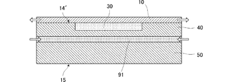
ここで、S104の分離形成工程において支持基板50には、図6(C)に示すように、圧縮応力膜90が裏面15に形成された状態で、圧電薄膜10が表面14に形成される。このとき、圧縮応力膜90が支持基板50における圧電単結晶基板1側の面14を圧縮する。即ち、支持基板50では、圧縮応力膜90による圧縮応力と圧電薄膜10による圧縮応力とが釣り合った状態となる。そのため、支持基板50は、反りが生じず平らになる。
Here, in the separation formation step of S104, the piezoelectric
よって、分離形成工程では、圧電薄膜10による分離面への圧縮応力を起因とした分離が行われず、注入イオン元素のガス化を起因とした分離が行われる。そのため、圧電薄膜10の表面粗さの劣化を防止できる。実験では、圧縮応力膜90を形成しない特許文献1の製造方法では表面粗さRaが50〜100nmであるのに対し、圧縮応力膜90を形成した本実施形態の製造方法では表面粗さRaを10〜20nmにまで改善できることが明らかとなっている。また、圧電薄膜10による圧縮応力が分離面に局所的に発生することも無くなるため、分離後に支持基板50が割れることもない。
Therefore, in the separation formation step, separation due to the compressive stress on the separation surface by the piezoelectric
従って、この実施形態の圧電デバイスの製造方法によれば、圧電薄膜10の表面粗さの劣化と支持基板50の割れを防ぐことができる。
Therefore, according to the method for manufacturing a piezoelectric device of this embodiment, it is possible to prevent the surface roughness of the piezoelectric
また、圧電薄膜10を単結晶薄膜とすることで、スパッタ、蒸着、CVD法等で成膜される多結晶薄膜より圧電性に優れた薄膜を形成することができる。また、圧電単結晶基板1の結晶方位が圧電薄膜10の結晶方位となるため、圧電デバイスの特性に応じた結晶方位を有する圧電単結晶基板1を用意することで、該特性に応じた結晶方位を有する圧電薄膜10を形成できる。また、イオン注入、接合、分離により単結晶薄膜を形成しているため、1枚の圧電単結晶基板1から複数の圧電薄膜10を形成することができるため、単結晶の圧電材料を節約することができる。
In addition, by using the piezoelectric
なお、この実施形態ではS103の圧縮応力膜形成工程において、支持基板50における圧電単結晶基板1側の面14に対向する裏面15に圧縮応力膜90を形成しているが、実施の際は、支持基板50の当該裏面15側から水素イオンを注入することで、イオン注入部分100と同様のイオン注入層を支持基板50中に形成しても構わない。この場合、イオン注入層が支持基板50における圧電単結晶基板1側の面14を圧縮する。即ち、支持基板50では、イオン注入層による圧縮応力と圧電薄膜10による圧縮応力とが釣り合った状態となる。そのため、この場合でも支持基板50は、反りが生じず平らになるため、この実施形態の製造方法と同様の効果を奏する。
In this embodiment, in the compressive stress film forming step of S103, the
次に、分離形成した圧電薄膜10の表面をCMP処理等により研磨して平坦化する(図3:S105)。この表面粗さは、算術平均粗さRaで0.5nm以下が好ましい。
次に、図7(A)に示すように、圧電薄膜10の表面上に、Al(アルミニウム)等を用いて、所定膜厚の上部電極60A,60BとIDT(InterdigitalTransducer)電極60Cを形成する(図3:S106)。ここで、上部電極60A、60BとIDT電極60Cが、本発明の「電極膜」に相当する。
なお、電極60A〜60Cには、Alのみでなく、デバイスの仕様に応じて、Al,W、Mo、Ta、Hf、Cu、Pt、Ti、Au等を単体もしくは複数積層して用いてもよい。Next, the surface of the separated piezoelectric
Next, as shown in FIG. 7A,
The
次に、図7(B)に示すように、圧電薄膜10及び電極60A〜60Cを保護するため、圧電薄膜10及び電極60A〜60Cの表面に絶縁膜70を形成する(図3:S107)。
Next, as shown in FIG. 7B, in order to protect the piezoelectric
次に、図8(A)に示すように、絶縁膜70の上部電極60A,60Bを露出させる領域に開口部82A、82Bをエッチング等で形成する(図3:S108)。
Next, as shown in FIG. 8A,
次に、図8(B)に示すように、外部端子を形成する(図3:S109)。詳述すると、上部電極60A、60B上にバンプパッド61A、61Bを形成し、両バンプパッド61A、61B上にバンプ62A、62Bを形成する。
Next, as shown in FIG. 8B, external terminals are formed (FIG. 3: S109). More specifically,
最後に、支持基板50上に形成された複数の薄膜型圧電デバイスから個別の薄膜型圧電デバイスに分割する分割工程を経て、モールド金型を用いたパッケージングを行う。このようにして薄膜型圧電デバイスを形成する。そのため、複数の薄膜型圧電デバイスを一括製造できる。従って、この実施形態によれば、複数の薄膜型圧電デバイスを一括製造できるため、薄膜型圧電デバイスの製造コストを大幅に削減できる。
Finally, packaging using a mold is performed through a dividing step of dividing a plurality of thin film piezoelectric devices formed on the
以上の製造方法で製造された圧電デバイスは、図8(B)に示すように、支持基板50と、イオンを注入された圧電単結晶基板1からイオン注入部分100で分離して支持基板50上に形成された単結晶の圧電薄膜10であって支持基板50上に接合された圧電薄膜10と、圧電薄膜10上に形成されたIDT電極膜60Cと、を備える。さらに、当該圧電デバイスは、支持基板50の圧電薄膜10側の面に対向する裏面に形成され、支持基板50の圧電薄膜10側の面を圧縮する圧縮応力膜90を備える。圧縮応力膜90は、圧電薄膜10の支持基板50側に形成され、支持基板50の圧電薄膜10側の面を収縮させる。
As shown in FIG. 8 (B), the piezoelectric device manufactured by the above manufacturing method is separated from the supporting
この実施形態では、分離形成工程後に、圧縮応力膜90による圧縮応力と圧電薄膜10による圧縮応力とが釣り合った状態となる。よって、この構成の圧電デバイスにおいては、分離形成工程において、圧電単結晶薄膜10による分離面への圧縮応力を起因とした分離が行われず、注入イオン元素のガス化を起因とした分離が行われる。従って、この実施形態の圧電デバイスによれば、製造時における、圧電薄膜10の表面粗さの劣化と支持基板50の割れを防ぐことができる。
In this embodiment, after the separation forming step, the compressive stress due to the
次に、第2の実施形態に係る圧電デバイスの製造方法について、図を参照して説明する。なお、以下の説明では、圧電デバイスの製造方法として弾性表面波デバイスの製造方法を例に説明する。 Next, a method for manufacturing a piezoelectric device according to the second embodiment will be described with reference to the drawings. In the following description, a method for manufacturing a surface acoustic wave device will be described as an example of a method for manufacturing a piezoelectric device.
図9は、第2の実施形態に係る圧電デバイスの製造方法を示すフローチャートである。図10、図12、図13は、図9に示す圧電デバイスの製造工程を模式的に示す断面図である。図11は、引張応力膜形成工程を経た後の分離工程終了時に引張応力膜により支持基板の反りが発生しない様子を模式的に示す図である。 FIG. 9 is a flowchart showing a method for manufacturing a piezoelectric device according to the second embodiment. 10, FIG. 12, and FIG. 13 are cross-sectional views schematically showing manufacturing steps of the piezoelectric device shown in FIG. FIG. 11 is a diagram schematically illustrating a state in which the support substrate is not warped by the tensile stress film at the end of the separation process after the tensile stress film formation process.
この実施形態の圧電デバイスの製造方法が第1の実施形態に示した圧電デバイスの製造方法と相違する点は、引張応力膜形成工程(S202)を行い、その後に接合工程(S203)を行う点である。即ち、図9のS201、S204〜S209は、それぞれ第1の実施形態に示した図3のS101、S104〜S109と同じである。 The piezoelectric device manufacturing method of this embodiment is different from the piezoelectric device manufacturing method shown in the first embodiment in that a tensile stress film forming step (S202) is performed and then a bonding step (S203) is performed. It is. That is, S201 and S204 to S209 in FIG. 9 are the same as S101 and S104 to S109 in FIG. 3 shown in the first embodiment, respectively.
詳述すると、まず、S201のイオン注入工程を経た圧電単結晶基板1を用意する。
More specifically, first, the piezoelectric
次に、図10(A)に示すように、引張応力膜91を圧電単結晶基板1のイオン注入部分100側の面12に形成する(図9:S202)。そして、引張応力膜91の表面をCMP等により平坦化処理する。引張応力膜91は、支持基板50における圧電単結晶基板1側の面14を圧縮する膜、即ち支持基板50における圧電単結晶基板1側の面14を収縮させる応力層である。引張応力膜91は、例えば酸化シリコン、窒化シリコン、酸化アルミニウム、窒化アルミニウム、酸化亜鉛、酸化タンタルを利用する。引張応力膜91は、蒸着、スパッタリング、CVD等により、圧電単結晶基板1のイオン注入部分100側の面12に成膜される。ただし、いずれの成膜方法でも支持基板50における圧電単結晶基板1側の面14を引っ張る膜が成膜されるよう、材料や膜厚などの成膜条件を設定する。
Next, as shown in FIG. 10A, a
次に、図10(B)に示すように、支持基板50を圧電単結晶基板1に接合する(図9:S203)。なお、この接合方法は、第1の実施形態と同じである。
Next, as shown in FIG. 10B, the
次に、図10(C)に示す圧電単結晶基板1と支持基板50との接合体を(この実施形態では500℃まで)加熱し、イオン注入部分100を分離面とした分離を行う(図9:S204)。なお、この分離方法は、第1の実施形態と同じである。
Next, the joined body of the piezoelectric
ここで、上記S204の分離形成工程により、支持基板50の表面14には、引張応力膜91と単結晶の圧電薄膜10とがこの順に積層される。このとき、図11に示すように、引張応力膜91が圧電薄膜10を引っ張ることにより支持基板50における圧電単結晶基板1側の面14を圧縮する。即ち、支持基板50では、引張応力膜91による引張応力と圧電薄膜10による圧縮応力とが釣り合った状態となる。そのため、この実施形態においても分離後の支持基板50は、反りが生じず平らになる。
従って、この実施形態の圧電デバイスの製造方法によれば、第1の実施形態の圧電デバイスの製造方法と同様の効果を奏する。Here, the
Therefore, according to the piezoelectric device manufacturing method of this embodiment, the same effects as the piezoelectric device manufacturing method of the first embodiment can be obtained.
以後、S204の分離形成工程以降の全工程を経ると、図13(B)に示す構造を有する圧電デバイスが得られる。この圧電デバイスは、支持基板50と、イオンを注入された圧電単結晶基板1からイオン注入部分100で分離して支持基板50上に形成された単結晶の圧電薄膜10であって支持基板50上に接合された圧電薄膜10と、圧電薄膜10上に形成されたIDT電極膜60Cと、を備える。さらに、当該圧電デバイスは、圧電薄膜10と支持基板50との間に形成され、圧電薄膜10を引っ張る引張応力膜91を備える。引張応力膜91は、圧電薄膜10の支持基板50側に形成され、支持基板50の圧電薄膜10側の面を収縮させる。
Thereafter, through all steps after the separation forming step of S204, a piezoelectric device having the structure shown in FIG. 13B is obtained. This piezoelectric device is a single-crystal piezoelectric
この実施形態では、分離形成工程後に、引張応力膜91による引張応力と圧電薄膜10による圧縮応力とが釣り合った状態となる。よって、この構成の圧電デバイスにおいては、分離形成工程において、圧電単結晶薄膜10による分離面への圧縮応力を起因とした分離が行われず、注入イオン元素のガス化を起因とした分離が行われる。従って、この実施形態の圧電デバイスによれば、製造時における、圧電薄膜10の表面粗さの劣化と支持基板50の割れを防ぐことができる。
In this embodiment, after the separation forming step, the tensile stress by the
次に、第3の実施形態に係る圧電デバイスの製造方法について、図を参照して説明する。 Next, a method for manufacturing a piezoelectric device according to the third embodiment will be described with reference to the drawings.
図14は、第3の実施形態に係る圧電デバイスの製造方法を示すフローチャートである。図15、図17は、図14に示す圧電デバイスの製造工程を模式的に示す断面図である。図16は、引張応力膜形成工程を経た後の分離工程終了時に引張応力膜により支持基板の反りが発生しない様子を模式的に示す図である。なお、以下の説明では、圧電デバイスの製造方法として、板波デバイス(図17参照)などのメンブレン構造を持つ圧電デバイスの製造方法を例に説明する。 FIG. 14 is a flowchart showing a method for manufacturing a piezoelectric device according to the third embodiment. 15, FIG. 17 is a cross-sectional view showing a manufacturing process of the piezoelectric device shown in FIG. 1 4 schematically. FIG. 16 is a diagram schematically illustrating a state in which the support substrate is not warped by the tensile stress film at the end of the separation process after the tensile stress film formation process. In the following description, as a method for manufacturing a piezoelectric device, a method for manufacturing a piezoelectric device having a membrane structure such as a plate wave device (see FIG. 17) will be described as an example.
この実施形態の圧電デバイスの製造方法は、図14のS301、S307〜S309、S312の工程が図9のS201、S205〜S207、S209の工程と共通し、その他の工程(S302〜S306、S310、S311)が相違するものである。 In the piezoelectric device manufacturing method of this embodiment, the steps S301, S307 to S309, and S312 in FIG. 14 are the same as the steps S201, S205 to S207, and S209 in FIG. S311) is different.
まず、S301のイオン注入工程を経た圧電単結晶基板1を用意する。
そして、圧電単結晶基板1におけるイオン注入部分100側の面12に、所定膜厚の犠牲層30を形成する(図14:S302)。犠牲層30は、具体的には、Ni,Cu,Al等の金属膜や、SiO2、ZnO、PSG(リンケイ酸ガラス)等の絶縁膜や、有機膜等から、条件に応じて適宜設定する。犠牲層30は、蒸着、スパッタリング、CVD、スピン塗布等により、支持基板50の表面上における空隙層80となる空間(即ち、圧電薄膜10が圧電デバイスとして機能する振動領域および孔部81A、81Bの直下の空間)に、成膜される。なお、実施の際は、犠牲層30を引張応力膜となるよう形成しても構わない。
First, the piezoelectric
Then, a
次に、圧電単結晶基板1におけるイオン注入部分100側の面12に、図15(A)に示すように、所定膜厚の支持層40を形成する(図14:S303)。支持層40は、絶縁性材料からなり、シリコン酸化物や窒化物、アルミニウム酸化物、PSG等の無機物や、樹脂等の有機物を利用し、犠牲層30の除去のためのエッチングガスやエッチング液に対して強い耐性を有するものであればよい。支持層40は、蒸着、スパッタリング、CVD、スピン塗布等により、支持基板50の表面の一定領域(犠牲層30を形成する領域を除外した領域)に成膜される。即ち、この支持層40は、圧電薄膜10が圧電デバイスとして機能しない非振動領域の直下に形成される。そして、支持層40の膜厚は、メンブレンの中空領域を構成する空隙層80の深さに応じて平坦化される。
なお、支持層40は、圧電単結晶基板1や犠牲層30に対して、線膨張係数を加味した上で材質を決定するとよりよい。Next, as shown in FIG. 15A, a
The material of the
次に、図15(B)に示すように、引張応力膜91を圧電単結晶基板1の犠牲層30及び支持層40の表面に形成する(図14:S304)。そして、引張応力膜91の表面をCMP等により平坦化処理する。引張応力膜91の形成方法は、図9のS202と同じである。
Next, as shown in FIG. 15B, a
次に、図15(C)に示すように、支持基板50を圧電単結晶基板1上の引張応力膜91の表面に接合する(図14:S305)。なお、この接合方法は、第2の実施形態と同じである。
Next, as shown in FIG. 15C, the
次に、図15(C)に示す圧電単結晶基板1と支持基板50とを接合した接合体を(この実施形態では500℃まで)加熱し、イオン注入部分100を分離面とした分離を行う(図14:S306)。なお、この分離方法は、第2の実施形態と同じである。
Next, the bonded body obtained by bonding the piezoelectric
ここで、上記S306の分離形成工程により、支持基板50の犠牲層30及び支持層40の表面14′には、単結晶の圧電薄膜10が形成される(図16参照)。このとき、図16に示すように、引張応力膜91が支持基板50の犠牲層30及び支持層40の面14′を圧縮する。即ち、支持基板50では、引張応力膜91による引張応力と圧電薄膜10による圧縮応力とが釣り合った状態となる。そのため、この実施形態においても支持基板50は、反りが生じず平らになる。
従って、この実施形態の圧電デバイスの製造方法によれば、第1の実施形態の圧電デバイスの製造方法と同様の効果を奏する。
Here, the single crystal piezoelectric
Therefore, according to the piezoelectric device manufacturing method of this embodiment, the same effects as the piezoelectric device manufacturing method of the first embodiment can be obtained.
次に、第2の実施形態の製造方法と同様に、ポリッシング(S307)、図17に示すような上部電極60A,60BとIDT電極60Cの形成(S308)、絶縁膜の形成(S309)を行う。
Next, similarly to the manufacturing method of the second embodiment, polishing (S307), formation of the
次に、フォトリソグラフィ技術を用いてレジスト膜をパターニングした後、エッチングガスを流入させることで、犠牲層30の一部を圧電薄膜10の表面側に露出させる孔部81A,81Bを形成する(図14:S310)。
Next, after patterning the resist film using a photolithographic technique, an etching gas is introduced to form
そして、エッチングガスもしくはエッチング液を孔部81A,81Bを介して流入させることで、犠牲層30を除去する(図14:S311)。これにより、犠牲層30が形成されていた空間は、図17に示すような空隙層80となる。
Then, the
次に、第2の実施形態の圧電デバイスの製造方法と同様に、外部端子を形成する(図14:S312)。 Next, external terminals are formed as in the piezoelectric device manufacturing method of the second embodiment (FIG. 14: S312).
最後に、支持基板50上に形成された複数の薄膜型圧電デバイスから個別の薄膜型圧電デバイスに分割する分割工程を経て、モールド金型を用いたパッケージングを行う。これにより、図17に示す構造を有する圧電デバイスが得られる。この圧電デバイスは、支持基板50と空隙層80と支持層40とからなる支持体と、イオンを注入された圧電単結晶基板1からイオン注入部分100で分離して支持体上に形成された単結晶の圧電薄膜10であって支持体上に接合された圧電薄膜10と、圧電薄膜10上に形成されたIDT電極膜60Cと、を備える。さらに、当該圧電デバイスは、圧電薄膜10と支持体との間に形成され、圧電薄膜10を引っ張る引張応力膜91を備える。引張応力膜91は、圧電薄膜10の支持体側に形成され、支持体の圧電薄膜10側の面を収縮させる。
Finally, packaging using a mold is performed through a dividing step of dividing a plurality of thin film piezoelectric devices formed on the
この実施形態では、分離形成工程後に、引張応力膜91による引張応力と圧電薄膜10による圧縮応力とが釣り合った状態となる。よって、この構成の圧電デバイスにおいては、分離形成工程において、圧電単結晶薄膜10による分離面への圧縮応力を起因とした分離が行われず、注入イオン元素のガス化を起因とした分離が行われる。従って、この実施形態の圧電デバイスによれば、製造時における、圧電薄膜10の表面粗さの劣化と支持基板50の割れを防ぐことができる。
In this embodiment, after the separation forming step, the tensile stress by the
なお、上述の実施形態では、板波デバイスを例に説明したが、他に、ジャイロ、RFスイッチ、振動発電素子等、圧電単結晶薄膜からなりメンブレンを有する各種デバイスに対しても、本発明の製造方法を適用することができる。 In the above-described embodiment, a plate wave device has been described as an example. However, the present invention is also applicable to various devices having a membrane made of a piezoelectric single crystal thin film such as a gyro, an RF switch, and a vibration power generation element. A manufacturing method can be applied.
また、上述の各実施形態の説明は、すべての点で例示であって、制限的なものではないと考えられるべきである。本発明の範囲は、上述の実施形態ではなく、特許請求の範囲によって示される。さらに、本発明の範囲には、特許請求の範囲と均等の意味および範囲内でのすべての変更が含まれることが意図される。 Moreover, it should be thought that description of each above-mentioned embodiment is an illustration in all the points, Comprising: It is not restrictive. The scope of the present invention is shown not by the above embodiments but by the claims. Furthermore, the scope of the present invention is intended to include all modifications within the meaning and scope equivalent to the scope of the claims.
1 圧電単結晶基板
4 裏面
5 圧電基板
6 イオン注入層
7 表面
8 結合材
9 支持基板
10 圧電薄膜
20 下部電極膜
21 誘電体膜
22 接合膜
30 犠牲層
40 支持層
50 支持基板
60A、60B 上部電極膜
60C IDT電極膜
61A、61B バンプパッド
62A、62B バンプ
63A 引き回し配線
63B、63C 上部電極膜
70 絶縁膜
80 空隙層
81A,81B 孔部
82A,82B 開口部
90 圧縮応力膜
91 引張応力膜
100 イオン注入部分
DESCRIPTION OF
Claims (13)
イオン化した元素を注入された圧電単結晶基板から、注入された元素の濃度がピークとなる部分を分離面とした分離を行って前記支持体上に形成された圧電単結晶薄膜と、
前記圧電単結晶薄膜上に形成された電極膜と、
前記支持体の前記圧電単結晶薄膜側の面を収縮させる応力層と、を備える圧電デバイス。A support;
A piezoelectric single crystal thin film formed on the support by performing separation using a portion where the concentration of the injected element is a peak as a separation surface from the piezoelectric single crystal substrate into which the ionized element is implanted;
An electrode film formed on the piezoelectric single crystal thin film;
And a stress layer for contracting a surface of the support on the piezoelectric single crystal thin film side.
圧電単結晶基板にイオン化した元素を注入することで、前記圧電単結晶基板の中に注入された元素の濃度がピークとなる部分を形成するイオン注入工程と、
前記支持体を前記圧電単結晶基板のイオン注入面側に形成する支持体形成工程と、
前記支持体の前記圧電単結晶薄膜側の面を収縮させる応力層を形成する応力層形成工程と、
前記注入された元素の濃度がピークとなる部分を分離面とした分離を前記圧電単結晶基板に対して行い、前記圧電単結晶薄膜を前記支持体上に形成する分離形成工程と、を有する圧電デバイスの製造方法。A method for manufacturing a piezoelectric device comprising: a support; and a piezoelectric single crystal thin film formed on the support,
An ion implantation step of forming a portion in which the concentration of the implanted element is peaked in the piezoelectric single crystal substrate by injecting an ionized element into the piezoelectric single crystal substrate;
Forming a support on the ion implantation surface side of the piezoelectric single crystal substrate; and
A stress layer forming step of forming a stress layer for contracting the surface of the support on the piezoelectric single crystal thin film side;
A separation forming step of separating the piezoelectric single crystal substrate from the portion where the concentration of the implanted element reaches a peak as a separation surface, and forming the piezoelectric single crystal thin film on the support. Device manufacturing method.
前記応力層形成工程は、前記圧電単結晶薄膜を引っ張る引張応力膜を前記応力層として前記圧電単結晶基板の前記イオン注入面側に形成する、請求項8に記載の圧電デバイスの製造方法。The support forming step is performed after the stress layer forming step,
9. The method of manufacturing a piezoelectric device according to claim 8, wherein in the stress layer forming step, a tensile stress film that pulls the piezoelectric single crystal thin film is formed as the stress layer on the ion implantation surface side of the piezoelectric single crystal substrate.
前記圧電結晶薄膜をエッチングし、前記犠牲層の一部を前記圧電薄膜の表面側に露出させる孔部を形成する露出工程と、
前記孔部を介して前記犠牲層を除去する犠牲層除去工程と、を有する、請求項8から12のいずれか1項に記載の圧電デバイスの製造方法。A sacrificial layer forming step of forming a sacrificial layer in a space serving as a void layer formed between the piezoelectric single crystal thin film and the support;
An exposure step of etching the piezoelectric crystal thin film to form a hole that exposes a portion of the sacrificial layer to the surface side of the piezoelectric thin film;
The method for manufacturing a piezoelectric device according to claim 8, further comprising a sacrificial layer removing step of removing the sacrificial layer through the hole.
Priority Applications (1)
| Application Number | Priority Date | Filing Date | Title |
|---|---|---|---|
| JP2012536502A JP5522263B2 (en) | 2010-09-28 | 2011-09-28 | Piezoelectric device and method for manufacturing piezoelectric device |
Applications Claiming Priority (4)
| Application Number | Priority Date | Filing Date | Title |
|---|---|---|---|
| JP2010216936 | 2010-09-28 | ||
| JP2010216936 | 2010-09-28 | ||
| PCT/JP2011/072161 WO2012043616A1 (en) | 2010-09-28 | 2011-09-28 | Piezoelectric device and method for manufacturing piezoelectric device |
| JP2012536502A JP5522263B2 (en) | 2010-09-28 | 2011-09-28 | Piezoelectric device and method for manufacturing piezoelectric device |
Publications (2)
| Publication Number | Publication Date |
|---|---|
| JPWO2012043616A1 JPWO2012043616A1 (en) | 2014-02-24 |
| JP5522263B2 true JP5522263B2 (en) | 2014-06-18 |
Family
ID=45893055
Family Applications (1)
| Application Number | Title | Priority Date | Filing Date |
|---|---|---|---|
| JP2012536502A Active JP5522263B2 (en) | 2010-09-28 | 2011-09-28 | Piezoelectric device and method for manufacturing piezoelectric device |
Country Status (4)
| Country | Link |
|---|---|
| US (2) | US9647199B2 (en) |
| EP (1) | EP2624451B1 (en) |
| JP (1) | JP5522263B2 (en) |
| WO (1) | WO2012043616A1 (en) |
Cited By (1)
| Publication number | Priority date | Publication date | Assignee | Title |
|---|---|---|---|---|
| KR20200078635A (en) * | 2018-03-14 | 2020-07-01 | 레이던 컴퍼니 | Stress compensation and relaxation of bonding wafers |
Families Citing this family (9)
| Publication number | Priority date | Publication date | Assignee | Title |
|---|---|---|---|---|
| JP6288110B2 (en) * | 2013-12-27 | 2018-03-07 | 株式会社村田製作所 | Elastic wave device |
| SG11201804271QA (en) * | 2015-11-20 | 2018-06-28 | Sunedison Semiconductor Ltd | Manufacturing method of smoothing a semiconductor surface |
| US9978582B2 (en) * | 2015-12-16 | 2018-05-22 | Ostendo Technologies, Inc. | Methods for improving wafer planarity and bonded wafer assemblies made from the methods |
| US10483248B2 (en) * | 2017-03-23 | 2019-11-19 | Skyworks Solutions, Inc. | Wafer level chip scale filter packaging using semiconductor wafers with through wafer vias |
| TWI780103B (en) * | 2017-05-02 | 2022-10-11 | 日商日本碍子股份有限公司 | Elastic wave element and method of manufacturing the same |
| CN110945971B (en) * | 2017-08-24 | 2023-09-26 | 阿莫善斯有限公司 | Method for manufacturing ceramic substrate and ceramic substrate |
| KR102222096B1 (en) * | 2017-09-15 | 2021-03-04 | 엔지케이 인슐레이터 엘티디 | Acoustic wave element and its manufacturing method |
| JP7439415B2 (en) | 2019-08-28 | 2024-02-28 | 住友金属鉱山株式会社 | Piezoelectric substrate, piezoelectric substrate manufacturing method, and composite substrate |
| CN112467024B (en) * | 2020-11-24 | 2023-04-07 | 上海新硅聚合半导体有限公司 | Preparation method of heterostructure thin film substrate |
Family Cites Families (14)
| Publication number | Priority date | Publication date | Assignee | Title |
|---|---|---|---|---|
| JPH08330882A (en) * | 1995-06-02 | 1996-12-13 | Sumitomo Electric Ind Ltd | Surface acoustic wave element substrate and its manufacture |
| JP2000091663A (en) * | 1998-09-17 | 2000-03-31 | Osaka Gas Co Ltd | Method for working silicon micro-device |
| FR2788176B1 (en) | 1998-12-30 | 2001-05-25 | Thomson Csf | GUIDED ACOUSTIC WAVE DEVICE IN A THIN LAYER OF PIEZOELECTRIC MATERIAL ADHESED BY A MOLECULAR ADHESIVE ONTO A CARRIER SUBSTRATE AND MANUFACTURING METHOD |
| FR2789518B1 (en) * | 1999-02-10 | 2003-06-20 | Commissariat Energie Atomique | MULTILAYER STRUCTURE WITH INTERNAL CONTROLLED STRESSES AND METHOD FOR PRODUCING SUCH A STRUCTURE |
| JP2000244030A (en) * | 1999-02-23 | 2000-09-08 | Mitsubishi Electric Corp | Piezoelectric thin film element |
| JP2003017967A (en) * | 2001-06-29 | 2003-01-17 | Toshiba Corp | Surface acoustic wave element and its manufacturing method |
| JP4830418B2 (en) * | 2005-09-16 | 2011-12-07 | 株式会社デンソー | Semiconductor device |
| JP2007181185A (en) * | 2005-12-01 | 2007-07-12 | Sony Corp | Acoustic resonator and its fabricating method |
| FR2924273B1 (en) * | 2007-11-28 | 2010-02-19 | Commissariat Energie Atomique | DEFORMATION MODERATION METHOD |
| JP4743258B2 (en) * | 2008-10-31 | 2011-08-10 | 株式会社村田製作所 | Method for manufacturing piezoelectric device |
| EP2377176B1 (en) * | 2008-12-17 | 2016-12-14 | Analog Devices, Inc. | Mechanical resonating structures including a temperature compensation structure |
| JP5212484B2 (en) | 2009-01-15 | 2013-06-19 | 株式会社村田製作所 | Piezoelectric device and method for manufacturing piezoelectric device |
| WO2011004665A1 (en) * | 2009-07-07 | 2011-01-13 | 株式会社村田製作所 | Elastic wave device and manufacturing method of elastic wave device |
| JP5429200B2 (en) * | 2010-05-17 | 2014-02-26 | 株式会社村田製作所 | Method for manufacturing composite piezoelectric substrate and piezoelectric device |
-
2011
- 2011-09-28 WO PCT/JP2011/072161 patent/WO2012043616A1/en active Application Filing
- 2011-09-28 JP JP2012536502A patent/JP5522263B2/en active Active
- 2011-09-28 EP EP11829169.9A patent/EP2624451B1/en active Active
-
2013
- 2013-03-26 US US13/850,520 patent/US9647199B2/en active Active
-
2017
- 2017-03-30 US US15/473,661 patent/US10707406B2/en active Active
Cited By (2)
| Publication number | Priority date | Publication date | Assignee | Title |
|---|---|---|---|---|
| KR20200078635A (en) * | 2018-03-14 | 2020-07-01 | 레이던 컴퍼니 | Stress compensation and relaxation of bonding wafers |
| KR102515211B1 (en) | 2018-03-14 | 2023-03-29 | 레이던 컴퍼니 | Stress Compensation and Relief of Bonded Wafers |
Also Published As
| Publication number | Publication date |
|---|---|
| US9647199B2 (en) | 2017-05-09 |
| US20170200882A1 (en) | 2017-07-13 |
| US10707406B2 (en) | 2020-07-07 |
| EP2624451A1 (en) | 2013-08-07 |
| US20130307372A1 (en) | 2013-11-21 |
| EP2624451B1 (en) | 2017-06-07 |
| WO2012043616A1 (en) | 2012-04-05 |
| EP2624451A4 (en) | 2015-03-11 |
| JPWO2012043616A1 (en) | 2014-02-24 |
Similar Documents
| Publication | Publication Date | Title |
|---|---|---|
| JP5522263B2 (en) | Piezoelectric device and method for manufacturing piezoelectric device | |
| JP5447682B2 (en) | Method for manufacturing piezoelectric device | |
| US9508918B2 (en) | Method for manufacturing piezoelectric device with a composite piezoelectric substrate | |
| US9240540B2 (en) | Piezoelectric device | |
| JP5510465B2 (en) | Piezoelectric device and method for manufacturing piezoelectric device | |
| JP6043717B2 (en) | Method of embedding piezoelectric material | |
| JP5152410B2 (en) | Method for manufacturing piezoelectric device | |
| JP5796316B2 (en) | Method for manufacturing piezoelectric device | |
| JP5817830B2 (en) | Piezoelectric bulk wave device and manufacturing method thereof | |
| WO2012128268A1 (en) | Piezoelectric device and manufacturing method for piezoelectric device | |
| JP5182379B2 (en) | Manufacturing method of composite substrate | |
| JP5277999B2 (en) | Manufacturing method of composite substrate | |
| JP2012074462A (en) | Piezoelectric device manufacturing method | |
| WO2011074329A1 (en) | Method for manufacturing piezoelectric device |
Legal Events
| Date | Code | Title | Description |
|---|---|---|---|
| A131 | Notification of reasons for refusal |
Free format text: JAPANESE INTERMEDIATE CODE: A131 Effective date: 20131203 |
|
| TRDD | Decision of grant or rejection written | ||
| A01 | Written decision to grant a patent or to grant a registration (utility model) |
Free format text: JAPANESE INTERMEDIATE CODE: A01 Effective date: 20140311 |
|
| A61 | First payment of annual fees (during grant procedure) |
Free format text: JAPANESE INTERMEDIATE CODE: A61 Effective date: 20140324 |
|
| R150 | Certificate of patent or registration of utility model |
Ref document number: 5522263 Country of ref document: JP Free format text: JAPANESE INTERMEDIATE CODE: R150 |