EP3675359A2 - Phaseninterpolator - Google Patents
Phaseninterpolator Download PDFInfo
- Publication number
- EP3675359A2 EP3675359A2 EP19219260.7A EP19219260A EP3675359A2 EP 3675359 A2 EP3675359 A2 EP 3675359A2 EP 19219260 A EP19219260 A EP 19219260A EP 3675359 A2 EP3675359 A2 EP 3675359A2
- Authority
- EP
- European Patent Office
- Prior art keywords
- phase
- adjusting module
- mos transistor
- signal
- circuit
- Prior art date
- Legal status (The legal status is an assumption and is not a legal conclusion. Google has not performed a legal analysis and makes no representation as to the accuracy of the status listed.)
- Pending
Links
Images


Classifications
-
- H—ELECTRICITY
- H04—ELECTRIC COMMUNICATION TECHNIQUE
- H04L—TRANSMISSION OF DIGITAL INFORMATION, e.g. TELEGRAPHIC COMMUNICATION
- H04L7/00—Arrangements for synchronising receiver with transmitter
- H04L7/02—Speed or phase control by the received code signals, the signals containing no special synchronisation information
- H04L7/033—Speed or phase control by the received code signals, the signals containing no special synchronisation information using the transitions of the received signal to control the phase of the synchronising-signal-generating means, e.g. using a phase-locked loop
- H04L7/0337—Selecting between two or more discretely delayed clocks or selecting between two or more discretely delayed received code signals
-
- H—ELECTRICITY
- H03—ELECTRONIC CIRCUITRY
- H03K—PULSE TECHNIQUE
- H03K5/00—Manipulating of pulses not covered by one of the other main groups of this subclass
- H03K5/13—Arrangements having a single output and transforming input signals into pulses delivered at desired time intervals
- H03K5/135—Arrangements having a single output and transforming input signals into pulses delivered at desired time intervals by the use of time reference signals, e.g. clock signals
-
- H—ELECTRICITY
- H04—ELECTRIC COMMUNICATION TECHNIQUE
- H04L—TRANSMISSION OF DIGITAL INFORMATION, e.g. TELEGRAPHIC COMMUNICATION
- H04L7/00—Arrangements for synchronising receiver with transmitter
- H04L7/0016—Arrangements for synchronising receiver with transmitter correction of synchronization errors
- H04L7/002—Arrangements for synchronising receiver with transmitter correction of synchronization errors correction by interpolation
- H04L7/0025—Arrangements for synchronising receiver with transmitter correction of synchronization errors correction by interpolation interpolation of clock signal
-
- H—ELECTRICITY
- H03—ELECTRONIC CIRCUITRY
- H03K—PULSE TECHNIQUE
- H03K5/00—Manipulating of pulses not covered by one of the other main groups of this subclass
- H03K2005/00013—Delay, i.e. output pulse is delayed after input pulse and pulse length of output pulse is dependent on pulse length of input pulse
- H03K2005/00019—Variable delay
- H03K2005/00026—Variable delay controlled by an analog electrical signal, e.g. obtained after conversion by a D/A converter
- H03K2005/00052—Variable delay controlled by an analog electrical signal, e.g. obtained after conversion by a D/A converter by mixing the outputs of fixed delayed signals with each other or with the input signal
Definitions
- the invention relates to the technical field of high-speed data transmission, and more particularly, to a phase interpolator.
- the phase interpolator is a device for adjusting the phase of a circuit clock and has been widely used in the related field.
- the phase interpolator is a device capable of mixing two input periodic clocks with the same frequency and different phases in proportion to generate an output clock signal with the same frequency and the phase between the two input periodic clocks. In practice, a requirement will be imposed that gears of the phase interpolator need to be switched.
- the conventional phase interpolator is a current steering phase interpolator.
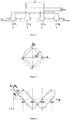
- a clock at the middle phase of the two IQ clocks is obtained by selecting different current weights of two adjacent IQ clocks signals in the circuit, as shown in Figure 1 .
- a1 and a2 refer to weights of two input phases, wherein ideal weighting factors a1 and a2 are indicated by dashed lines, and conventional weighting factors a1 and a2 are indicated by solid lines.
- Figure 3 shows a relationship between the weighting factors a1 and a2 of the conventional phase interpolator and the phase angle ⁇ .
- the present invention provides a phase interpolator.
- a phase interpolator comprising:
- phase interpolator further comprises a low-pass filter circuit
- an input end of the low-pass filter circuit is connected to an output end of the phase adjusting circuit
- the low-pass filter circuit is configured to filter a high-frequency signal of the interpolation signal.
- the phase interpolator further comprises a shaping circuit
- an input end of the shaping circuit is connected to an output end of the low-pass filter circuit
- the shaping circuit is configured to shape the interpolation signal output by the low-pass filter circuit, so as to output a required interpolation signal.
- each of the first phase adjusting module and the second phase adjusting module comprises:
- the first adjusting module comprises a plurality of first adjusting circuits, each of which is connected between the first fulcrum and the signal output end.
- each of the plurality of first adjusting circuits comprises:
- the second adjusting module comprises a plurality of second adjusting circuits, each of which is connected between the second fulcrum and the signal output end.
- each of the plurality of second adjusting circuits comprises:
- both the first MOS transistor and the first switch tube are N-type MOS transistors.
- both the second MOS transistor and the second switch tube are P-type MOS transistors.
- the present invention has the beneficial effects that a phase interpolator is disclosed, by using a first phase adjustment module and a second phase adjustment module, a first clock signal and a second clock signal with the same frequency and different phases are mixed in proportion by adopting a voltage mode to generate an interpolation signal with the same frequency and the phase between the first clock signal and the second clock signal so as to achieve the purpose of phase adjustment, and meanwhile, the circuit can be carried out under lower voltage, so that the power consumption of the phase adjusting circuit is further reduced.
- the term "plurality” means a number greater than one.
- the conventional phase interpolator is a current steering phase interpolator.
- a clock at the middle phase of the two IQ clocks is obtained by selecting different current weights of two adjacent IQ clocks signals in the circuit, as shown in Figure 1 .
- Figures 2 and 3 when the above-mentioned circuit is applied to a high-speed circuit, due to the fact that all of the circuits are driven by current, larger current is needed for the fast switch of signals at a high speed; in the meantime, only when an input signal is preferably a sinusoidal signal can a better result be obtained, and the cost is relatively high.
- the present invention provides a phase interpolator.
- the phase interpolator comprises:
- a phase interpolator comprising a phase adjusting circuit 1.
- the phase adjusting circuit 1 consists of a first phase adjusting module 10 and a second phase adjusting module 12.
- a first clock signal and a second clock signal with the same frequency and different phases are mixed in proportion by adopting a voltage mode to generate an interpolation signal with the same frequency and the phase between the first clock signal and the second clock signal so as to achieve the purpose of phase adjustment, and meanwhile, the circuit can be carried out under lower voltage, so that the power consumption of the phase adjusting circuit is further reduced.
- the phase interpolator further comprises a low-pass filter circuit 2, an input end of the low-pass filter circuit 2 is connected to an output end of the phase adjusting circuit 1, the low-pass filter circuit 2 is configured to filter a high-frequency signal of the interpolation signal; and the phase interpolator further comprises a shaping circuit 3, an input end of the shaping circuit 3 is connected to an output end of the low-pass filter circuit 2, the shaping circuit 3 is configured to shape the interpolation signal output by the low-pass filter circuit 2, so as to output a required interpolation signal.
- a first clock signal and a second clock signal with the same frequency and different phases are mixed in proportion by adopting a voltage mode to generate an interpolation signal with the same frequency and the phase between the first clock signal and the second clock signal.
- the low-pass filter circuit 2 may consist of a first capacitor C1 and a third resistor R3, wherein the third resistor R3 is connected to the output end of the phase adjusting circuit 1, and the first capacitor C1 is connected between the third resistor R3 and the ground GND Shape, by the shaping circuit 3, the interpolation signal output by the low-pass filter circuit 2, so as to output a required interpolation signal.
- the shaping circuit 3 may consist of a second capacitor C2 and a shaping circuit 30, wherein the second capacitor C2 is connected in series with the shaping circuit 30, and is connected between the third resistor R3 and the output end of the phase adjusting circuit 1. In this way, phase adjustment is achieved, and meanwhile, the circuit can be carried out under lower voltage, so that the power consumption of the phase adjusting circuit is further reduced.
- each of the first phase adjusting module 10 and the second phase adjusting module 11 comprises:
- circuit diagrams of the first phase adjusting module 10 and the second phase adjusting module 11 are symmetrically distributed.
- the circuit diagrams comprise the signal input end Input, the signal output end Output, the first MOS transistor M1, the first adjusting module A1, the second MOS transistor M2, the second adjusting module A2, wherein the first MOS transistor M1 is a N-type MOS transistor, and the second MOS transistor M2 is a P-type MOS transistor.
- a first clock signal and a second clock signal with the same frequency and different phases are mixed in proportion by adopting a voltage mode to generate an interpolation signal with the same frequency and the phase between the first clock signal and the second clock signal so as to achieve the purpose of phase adjustment, and meanwhile, the circuit can be carried out under lower voltage, so that the power consumption of the phase adjusting circuit is further reduced.
- the first adjusting module A1 comprises a plurality of first adjusting circuits A10, each of which is connected between the first fulcrum Q1 and the signal output end Output; each of the plurality of first adjusting circuits A10 comprises:
- the first adjusting module A1 comprises a plurality of first adjusting circuits A10, and each of the plurality of first adjusting circuits A10 comprises the first switch tube T1 and the first resistor R1, the first switch tube T1 is a N-type MOS transistor. Voltage weights of the first adjusting module A1 can be adjusted by selecting different resistance values of the first resistor R1 through the first switch tube T1, so as to achieve the purpose of phase adjustment.
- a first clock signal and a second clock signal with the same frequency and different phases are mixed in proportion by adopting a voltage mode to generate an interpolation signal with the same frequency and the phase between the first clock signal and the second clock signal so as to achieve the purpose of phase adjustment, and meanwhile, the circuit can be carried out under lower voltage, so that the power consumption of the phase adjusting circuit is further reduced.
- the second adjusting module A2 comprises a plurality of second adjusting circuits A20, each of which is connected between the second fulcrum Q2 and the signal output end Output; each of the plurality of second adjusting circuits A2 comprises:
- the second adjusting module A2 comprises a plurality of second adjusting circuits A20, and each of the plurality of second adjusting circuits A20 comprises the second switch tube T2 and the second resistor R2, and the second switch tube T2 is a P-type MOS transistor. Voltage weights of the second adjusting module A2 can be adjusted by selecting different resistance values of the second resistor R2 through the second switch tube T2, so as to achieve the purpose of phase adjustment.
- a first clock signal and a second clock signal with the same frequency and different phases are mixed in proportion by adopting a voltage mode to generate an interpolation signal with the same frequency and the phase between the first clock signal and the second clock signal so as to achieve the purpose of phase adjustment, and meanwhile, the circuit can be carried out under lower voltage, so that the power consumption of the phase adjusting circuit is further reduced.
- each of the first phase adjusting module 10 and the second phase adjusting module 11 comprises:
- circuit diagrams of the first phase adjusting module 10 and the second phase adjusting module 11 are symmetrically distributed.
- the circuit diagrams comprise the signal input end Input, the signal output end Output, the first MOS transistor M1, the first adjusting module A1, the second MOS transistor M2, the second adjusting module A2, wherein the first MOS transistor M1 is a N-type MOS transistor, and the second MOS transistor M2 is a P-type MOS transistor.
- a first clock signal and a second clock signal with the same frequency and different phases are mixed in proportion by adopting a voltage mode to generate an interpolation signal with the same frequency and the phase between the first clock signal and the second clock signal so as to achieve the purpose of phase adjustment, and meanwhile, the circuit can be carried out under lower voltage, so that the power consumption of the phase adjusting circuit is further reduced.
- the first adjusting module A1 comprises a plurality of third adjusting circuits A10, each of which is connected between the third fulcrum Q3 and VCC; each of the plurality of first adjusting circuits A10 comprises:
- the first adjusting module A1 comprises a plurality of first adjusting circuits A10, and each of the plurality of first adjusting circuits A10 comprises the first switch tube T1 and the first resistor R1, and the first switch tube T1 is a N-type MOS transistor. Voltage weights of the first adjusting module A1 can be adjusted by selecting different resistance values of the first resistor R1 through the first switch tube T1, so as to achieve the purpose of phase adjustment.
- a first clock signal and a second clock signal with the same frequency and different phases are mixed in proportion by adopting a voltage mode to generate an interpolation signal with the same frequency and the phase between the first clock signal and the second clock signal so as to achieve the purpose of phase adjustment, and meanwhile, the circuit can be carried out under lower voltage, so that the power consumption of the phase adjusting circuit is further reduced.
- the second adjusting module A2 comprises a plurality of second adjusting circuits A20, each of which is connected between the fourth fulcrum Q4 and the ground (GND); each of the plurality of second adjusting circuits A2 comprises:
- the second adjusting module A2 comprises a plurality of second adjusting circuits A20, and each of the plurality of second adjusting circuits A20 comprises the second switch tube T2 and the second resistor R2, and the second switch tube T2 is a P-type MOS transistor. Voltage weights of the second adjusting module A2 can be adjusted by selecting different resistance values of the second resistor R2 through the second switch tube T2, so as to achieve the purpose of phase adjustment.
- a first clock signal and a second clock signal with the same frequency and different phases are mixed in proportion by adopting a voltage mode to generate an interpolation signal with the same frequency and the phase between the first clock signal and the second clock signal so as to achieve the purpose of phase adjustment, and meanwhile, the circuit can be carried out under lower voltage, so that the power consumption of the phase adjusting circuit is further reduced.
Landscapes
- Engineering & Computer Science (AREA)
- Computer Networks & Wireless Communication (AREA)
- Signal Processing (AREA)
- Physics & Mathematics (AREA)
- Nonlinear Science (AREA)
- Manipulation Of Pulses (AREA)
- Stabilization Of Oscillater, Synchronisation, Frequency Synthesizers (AREA)
- Dc Digital Transmission (AREA)
- Networks Using Active Elements (AREA)
- Electronic Switches (AREA)
Applications Claiming Priority (1)
| Application Number | Priority Date | Filing Date | Title |
|---|---|---|---|
| CN201811642621.4A CN109981086B (zh) | 2018-12-29 | 2018-12-29 | 一种相位插值器 |
Publications (2)
| Publication Number | Publication Date |
|---|---|
| EP3675359A2 true EP3675359A2 (de) | 2020-07-01 |
| EP3675359A3 EP3675359A3 (de) | 2020-07-08 |
Family
ID=67076431
Family Applications (1)
| Application Number | Title | Priority Date | Filing Date |
|---|---|---|---|
| EP19219260.7A Pending EP3675359A3 (de) | 2018-12-29 | 2019-12-23 | Phaseninterpolator |
Country Status (3)
| Country | Link |
|---|---|
| US (1) | US10848299B2 (de) |
| EP (1) | EP3675359A3 (de) |
| CN (1) | CN109981086B (de) |
Families Citing this family (7)
| Publication number | Priority date | Publication date | Assignee | Title |
|---|---|---|---|---|
| CN111010175B (zh) * | 2019-12-11 | 2021-06-29 | 浙江大学 | 一种高线性度相位插值器 |
| CN112994685B (zh) * | 2019-12-12 | 2022-08-16 | 上海交通大学 | 数字相位转换器提高输出线性度的方法 |
| CN110995212B (zh) * | 2019-12-19 | 2021-08-24 | 成都海光微电子技术有限公司 | 一种集成电路器件、相位插值器、接口电路及电子设备 |
| US11005467B1 (en) * | 2020-05-18 | 2021-05-11 | Realtek Semiconductor Corp. | Low-noise duty cycle correction circuit and method thereof |
| CN112350694B (zh) * | 2020-10-30 | 2022-09-06 | 上海兆芯集成电路有限公司 | 相位插值器 |
| TWI792643B (zh) * | 2021-10-29 | 2023-02-11 | 瑞昱半導體股份有限公司 | 相位內插器與相位緩衝器電路 |
| CN116846369A (zh) * | 2023-06-09 | 2023-10-03 | 高澈科技(上海)有限公司 | 相位插值器及电子设备 |
Family Cites Families (15)
| Publication number | Priority date | Publication date | Assignee | Title |
|---|---|---|---|---|
| KR20100037427A (ko) * | 2008-10-01 | 2010-04-09 | 삼성전자주식회사 | Ac 커플링 위상 보간기 및 이 장치를 이용하는 지연 고정루프 |
| KR20110003189A (ko) * | 2009-07-03 | 2011-01-11 | 삼성전자주식회사 | 듀티 사이클 에러 보정 회로 |
| KR101287224B1 (ko) * | 2009-08-24 | 2013-07-17 | 후지쯔 가부시끼가이샤 | 위상 인터폴레이터 및 반도체 회로 장치 |
| JP2011055048A (ja) * | 2009-08-31 | 2011-03-17 | Renesas Electronics Corp | 多相クロック生成回路 |
| US8035436B2 (en) * | 2009-09-24 | 2011-10-11 | Oracle America, Inc. | Passive capacitively injected phase interpolator |
| US20110241746A1 (en) * | 2010-03-30 | 2011-10-06 | Taiwan Semiconductor Manufacturing Co., Ltd. | Low power small area static phase interpolator with good linearity |
| KR101331441B1 (ko) * | 2012-06-29 | 2013-11-21 | 포항공과대학교 산학협력단 | 다단 위상믹서 회로 |
| US8873689B2 (en) * | 2012-08-02 | 2014-10-28 | Taiwan Semiconductor Manufacturing Co., Ltd. | Phase interpolator for clock data recovery circuit with active wave shaping integrators |
| US8896358B2 (en) * | 2012-11-08 | 2014-11-25 | Avago Technologies General Ip (Singapore) Pte. Ltd. | Phase interpolator having adaptively biased phase mixer |
| US9077511B2 (en) * | 2013-04-30 | 2015-07-07 | Intel Mobile Communications GmbH | Phase interpolator |
| US8908804B2 (en) * | 2013-04-30 | 2014-12-09 | Intel Mobile Communications GmbH | Phase interpolator |
| US9584304B2 (en) * | 2015-03-30 | 2017-02-28 | Global Unichip Corporation | Phase interpolator and clock and data recovery circuit |
| CN205385462U (zh) * | 2016-03-01 | 2016-07-13 | 成都锐成芯微科技有限责任公司 | 占空比矫正电路 |
| CN108923773A (zh) | 2018-06-27 | 2018-11-30 | 重庆湃芯入微科技有限公司 | 一种低功耗可调型高线性度相位插值器 |
| CN108832915B (zh) * | 2018-09-13 | 2024-05-14 | 长江存储科技有限责任公司 | 一种占空比校准电路 |
-
2018
- 2018-12-29 CN CN201811642621.4A patent/CN109981086B/zh active Active
-
2019
- 2019-12-23 EP EP19219260.7A patent/EP3675359A3/de active Pending
- 2019-12-27 US US16/728,487 patent/US10848299B2/en active Active
Also Published As
| Publication number | Publication date |
|---|---|
| CN109981086B (zh) | 2023-04-28 |
| CN109981086A (zh) | 2019-07-05 |
| US20200213077A1 (en) | 2020-07-02 |
| US10848299B2 (en) | 2020-11-24 |
| EP3675359A3 (de) | 2020-07-08 |
Similar Documents
| Publication | Publication Date | Title |
|---|---|---|
| EP3675359A2 (de) | Phaseninterpolator | |
| US20170163251A1 (en) | Phase interpolators and push-pull buffers | |
| KR101239709B1 (ko) | 반도체 메모리 장치의 듀티 사이클 보정 회로 | |
| US20070194805A1 (en) | Data output driving circuit of semiconductor memory apparatus | |
| US7570094B2 (en) | Automatic duty cycle correction circuit with programmable duty cycle target | |
| TWI519073B (zh) | 移位暫存器電路及其操作方法 | |
| KR20090024453A (ko) | 듀티 싸이클 보정 회로 | |
| US7705630B1 (en) | Negative voltage level shifter having simplified structure | |
| WO2019024803A1 (zh) | 电平移位电路和集成电路芯片 | |
| US20180302073A1 (en) | Duty cycle calibration circuit and frequency synthesizer using the same | |
| US9490758B2 (en) | Power amplifier | |
| US7501874B2 (en) | Level shift circuit | |
| US7652506B2 (en) | Complementary signal generating circuit | |
| US20120001663A1 (en) | Mixed-mode input buffer | |
| KR20020067736A (ko) | 위상혼합기 및 이를 이용한 다중위상 발생기 | |
| US6043679A (en) | Level shifter | |
| CN102427359B (zh) | 插值电路及插值系统 | |
| US9306551B2 (en) | Interpolator and interpolation cells with non-uniform driving capabilities therein | |
| US11368152B2 (en) | Source signal output circuit and inverter thereof | |
| US10305482B2 (en) | Voltage level shifter | |
| US7667520B2 (en) | Level shift device having reduced error in the duty ratio of the output signal | |
| KR100855274B1 (ko) | 유닛 딜레이 셀 및 이를 포함하는 지연 고정 루프 | |
| US8742807B1 (en) | Low supply voltage analog phase interpolator | |
| TWI813197B (zh) | 訊號轉換電路及其偏壓產生電路 | |
| US6714055B2 (en) | Output driver devices |
Legal Events
| Date | Code | Title | Description |
|---|---|---|---|
| PUAI | Public reference made under article 153(3) epc to a published international application that has entered the european phase |
Free format text: ORIGINAL CODE: 0009012 |
|
| STAA | Information on the status of an ep patent application or granted ep patent |
Free format text: STATUS: REQUEST FOR EXAMINATION WAS MADE |
|
| PUAL | Search report despatched |
Free format text: ORIGINAL CODE: 0009013 |
|
| 17P | Request for examination filed |
Effective date: 20191224 |
|
| AK | Designated contracting states |
Kind code of ref document: A2 Designated state(s): AL AT BE BG CH CY CZ DE DK EE ES FI FR GB GR HR HU IE IS IT LI LT LU LV MC MK MT NL NO PL PT RO RS SE SI SK SM TR |
|
| AX | Request for extension of the european patent |
Extension state: BA ME |
|
| AK | Designated contracting states |
Kind code of ref document: A3 Designated state(s): AL AT BE BG CH CY CZ DE DK EE ES FI FR GB GR HR HU IE IS IT LI LT LU LV MC MK MT NL NO PL PT RO RS SE SI SK SM TR |
|
| AX | Request for extension of the european patent |
Extension state: BA ME |
|
| RIC1 | Information provided on ipc code assigned before grant |
Ipc: H03K 5/00 20060101ALN20200529BHEP Ipc: H03K 5/135 20060101AFI20200529BHEP |