EP3675359A2 - Phase interpolator - Google Patents
Phase interpolator Download PDFInfo
- Publication number
- EP3675359A2 EP3675359A2 EP19219260.7A EP19219260A EP3675359A2 EP 3675359 A2 EP3675359 A2 EP 3675359A2 EP 19219260 A EP19219260 A EP 19219260A EP 3675359 A2 EP3675359 A2 EP 3675359A2
- Authority
- EP
- European Patent Office
- Prior art keywords
- phase
- adjusting module
- mos transistor
- signal
- circuit
- Prior art date
- Legal status (The legal status is an assumption and is not a legal conclusion. Google has not performed a legal analysis and makes no representation as to the accuracy of the status listed.)
- Pending
Links
Images


Classifications
-
- H—ELECTRICITY
- H04—ELECTRIC COMMUNICATION TECHNIQUE
- H04L—TRANSMISSION OF DIGITAL INFORMATION, e.g. TELEGRAPHIC COMMUNICATION
- H04L7/00—Arrangements for synchronising receiver with transmitter
- H04L7/02—Speed or phase control by the received code signals, the signals containing no special synchronisation information
- H04L7/033—Speed or phase control by the received code signals, the signals containing no special synchronisation information using the transitions of the received signal to control the phase of the synchronising-signal-generating means, e.g. using a phase-locked loop
- H04L7/0337—Selecting between two or more discretely delayed clocks or selecting between two or more discretely delayed received code signals
-
- H—ELECTRICITY
- H03—ELECTRONIC CIRCUITRY
- H03K—PULSE TECHNIQUE
- H03K5/00—Manipulating of pulses not covered by one of the other main groups of this subclass
- H03K5/13—Arrangements having a single output and transforming input signals into pulses delivered at desired time intervals
- H03K5/135—Arrangements having a single output and transforming input signals into pulses delivered at desired time intervals by the use of time reference signals, e.g. clock signals
-
- H—ELECTRICITY
- H04—ELECTRIC COMMUNICATION TECHNIQUE
- H04L—TRANSMISSION OF DIGITAL INFORMATION, e.g. TELEGRAPHIC COMMUNICATION
- H04L7/00—Arrangements for synchronising receiver with transmitter
- H04L7/0016—Arrangements for synchronising receiver with transmitter correction of synchronization errors
- H04L7/002—Arrangements for synchronising receiver with transmitter correction of synchronization errors correction by interpolation
- H04L7/0025—Arrangements for synchronising receiver with transmitter correction of synchronization errors correction by interpolation interpolation of clock signal
-
- H—ELECTRICITY
- H03—ELECTRONIC CIRCUITRY
- H03K—PULSE TECHNIQUE
- H03K5/00—Manipulating of pulses not covered by one of the other main groups of this subclass
- H03K2005/00013—Delay, i.e. output pulse is delayed after input pulse and pulse length of output pulse is dependent on pulse length of input pulse
- H03K2005/00019—Variable delay
- H03K2005/00026—Variable delay controlled by an analog electrical signal, e.g. obtained after conversion by a D/A converter
- H03K2005/00052—Variable delay controlled by an analog electrical signal, e.g. obtained after conversion by a D/A converter by mixing the outputs of fixed delayed signals with each other or with the input signal
Definitions
- the invention relates to the technical field of high-speed data transmission, and more particularly, to a phase interpolator.
- the phase interpolator is a device for adjusting the phase of a circuit clock and has been widely used in the related field.
- the phase interpolator is a device capable of mixing two input periodic clocks with the same frequency and different phases in proportion to generate an output clock signal with the same frequency and the phase between the two input periodic clocks. In practice, a requirement will be imposed that gears of the phase interpolator need to be switched.
- the conventional phase interpolator is a current steering phase interpolator.
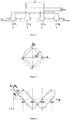
- a clock at the middle phase of the two IQ clocks is obtained by selecting different current weights of two adjacent IQ clocks signals in the circuit, as shown in Figure 1 .
- a1 and a2 refer to weights of two input phases, wherein ideal weighting factors a1 and a2 are indicated by dashed lines, and conventional weighting factors a1 and a2 are indicated by solid lines.
- Figure 3 shows a relationship between the weighting factors a1 and a2 of the conventional phase interpolator and the phase angle ⁇ .
- the present invention provides a phase interpolator.
- a phase interpolator comprising:
- phase interpolator further comprises a low-pass filter circuit
- an input end of the low-pass filter circuit is connected to an output end of the phase adjusting circuit
- the low-pass filter circuit is configured to filter a high-frequency signal of the interpolation signal.
- the phase interpolator further comprises a shaping circuit
- an input end of the shaping circuit is connected to an output end of the low-pass filter circuit
- the shaping circuit is configured to shape the interpolation signal output by the low-pass filter circuit, so as to output a required interpolation signal.
- each of the first phase adjusting module and the second phase adjusting module comprises:
- the first adjusting module comprises a plurality of first adjusting circuits, each of which is connected between the first fulcrum and the signal output end.
- each of the plurality of first adjusting circuits comprises:
- the second adjusting module comprises a plurality of second adjusting circuits, each of which is connected between the second fulcrum and the signal output end.
- each of the plurality of second adjusting circuits comprises:
- both the first MOS transistor and the first switch tube are N-type MOS transistors.
- both the second MOS transistor and the second switch tube are P-type MOS transistors.
- the present invention has the beneficial effects that a phase interpolator is disclosed, by using a first phase adjustment module and a second phase adjustment module, a first clock signal and a second clock signal with the same frequency and different phases are mixed in proportion by adopting a voltage mode to generate an interpolation signal with the same frequency and the phase between the first clock signal and the second clock signal so as to achieve the purpose of phase adjustment, and meanwhile, the circuit can be carried out under lower voltage, so that the power consumption of the phase adjusting circuit is further reduced.
- the term "plurality” means a number greater than one.
- the conventional phase interpolator is a current steering phase interpolator.
- a clock at the middle phase of the two IQ clocks is obtained by selecting different current weights of two adjacent IQ clocks signals in the circuit, as shown in Figure 1 .
- Figures 2 and 3 when the above-mentioned circuit is applied to a high-speed circuit, due to the fact that all of the circuits are driven by current, larger current is needed for the fast switch of signals at a high speed; in the meantime, only when an input signal is preferably a sinusoidal signal can a better result be obtained, and the cost is relatively high.
- the present invention provides a phase interpolator.
- the phase interpolator comprises:
- a phase interpolator comprising a phase adjusting circuit 1.
- the phase adjusting circuit 1 consists of a first phase adjusting module 10 and a second phase adjusting module 12.
- a first clock signal and a second clock signal with the same frequency and different phases are mixed in proportion by adopting a voltage mode to generate an interpolation signal with the same frequency and the phase between the first clock signal and the second clock signal so as to achieve the purpose of phase adjustment, and meanwhile, the circuit can be carried out under lower voltage, so that the power consumption of the phase adjusting circuit is further reduced.
- the phase interpolator further comprises a low-pass filter circuit 2, an input end of the low-pass filter circuit 2 is connected to an output end of the phase adjusting circuit 1, the low-pass filter circuit 2 is configured to filter a high-frequency signal of the interpolation signal; and the phase interpolator further comprises a shaping circuit 3, an input end of the shaping circuit 3 is connected to an output end of the low-pass filter circuit 2, the shaping circuit 3 is configured to shape the interpolation signal output by the low-pass filter circuit 2, so as to output a required interpolation signal.
- a first clock signal and a second clock signal with the same frequency and different phases are mixed in proportion by adopting a voltage mode to generate an interpolation signal with the same frequency and the phase between the first clock signal and the second clock signal.
- the low-pass filter circuit 2 may consist of a first capacitor C1 and a third resistor R3, wherein the third resistor R3 is connected to the output end of the phase adjusting circuit 1, and the first capacitor C1 is connected between the third resistor R3 and the ground GND Shape, by the shaping circuit 3, the interpolation signal output by the low-pass filter circuit 2, so as to output a required interpolation signal.
- the shaping circuit 3 may consist of a second capacitor C2 and a shaping circuit 30, wherein the second capacitor C2 is connected in series with the shaping circuit 30, and is connected between the third resistor R3 and the output end of the phase adjusting circuit 1. In this way, phase adjustment is achieved, and meanwhile, the circuit can be carried out under lower voltage, so that the power consumption of the phase adjusting circuit is further reduced.
- each of the first phase adjusting module 10 and the second phase adjusting module 11 comprises:
- circuit diagrams of the first phase adjusting module 10 and the second phase adjusting module 11 are symmetrically distributed.
- the circuit diagrams comprise the signal input end Input, the signal output end Output, the first MOS transistor M1, the first adjusting module A1, the second MOS transistor M2, the second adjusting module A2, wherein the first MOS transistor M1 is a N-type MOS transistor, and the second MOS transistor M2 is a P-type MOS transistor.
- a first clock signal and a second clock signal with the same frequency and different phases are mixed in proportion by adopting a voltage mode to generate an interpolation signal with the same frequency and the phase between the first clock signal and the second clock signal so as to achieve the purpose of phase adjustment, and meanwhile, the circuit can be carried out under lower voltage, so that the power consumption of the phase adjusting circuit is further reduced.
- the first adjusting module A1 comprises a plurality of first adjusting circuits A10, each of which is connected between the first fulcrum Q1 and the signal output end Output; each of the plurality of first adjusting circuits A10 comprises:
- the first adjusting module A1 comprises a plurality of first adjusting circuits A10, and each of the plurality of first adjusting circuits A10 comprises the first switch tube T1 and the first resistor R1, the first switch tube T1 is a N-type MOS transistor. Voltage weights of the first adjusting module A1 can be adjusted by selecting different resistance values of the first resistor R1 through the first switch tube T1, so as to achieve the purpose of phase adjustment.
- a first clock signal and a second clock signal with the same frequency and different phases are mixed in proportion by adopting a voltage mode to generate an interpolation signal with the same frequency and the phase between the first clock signal and the second clock signal so as to achieve the purpose of phase adjustment, and meanwhile, the circuit can be carried out under lower voltage, so that the power consumption of the phase adjusting circuit is further reduced.
- the second adjusting module A2 comprises a plurality of second adjusting circuits A20, each of which is connected between the second fulcrum Q2 and the signal output end Output; each of the plurality of second adjusting circuits A2 comprises:
- the second adjusting module A2 comprises a plurality of second adjusting circuits A20, and each of the plurality of second adjusting circuits A20 comprises the second switch tube T2 and the second resistor R2, and the second switch tube T2 is a P-type MOS transistor. Voltage weights of the second adjusting module A2 can be adjusted by selecting different resistance values of the second resistor R2 through the second switch tube T2, so as to achieve the purpose of phase adjustment.
- a first clock signal and a second clock signal with the same frequency and different phases are mixed in proportion by adopting a voltage mode to generate an interpolation signal with the same frequency and the phase between the first clock signal and the second clock signal so as to achieve the purpose of phase adjustment, and meanwhile, the circuit can be carried out under lower voltage, so that the power consumption of the phase adjusting circuit is further reduced.
- each of the first phase adjusting module 10 and the second phase adjusting module 11 comprises:
- circuit diagrams of the first phase adjusting module 10 and the second phase adjusting module 11 are symmetrically distributed.
- the circuit diagrams comprise the signal input end Input, the signal output end Output, the first MOS transistor M1, the first adjusting module A1, the second MOS transistor M2, the second adjusting module A2, wherein the first MOS transistor M1 is a N-type MOS transistor, and the second MOS transistor M2 is a P-type MOS transistor.
- a first clock signal and a second clock signal with the same frequency and different phases are mixed in proportion by adopting a voltage mode to generate an interpolation signal with the same frequency and the phase between the first clock signal and the second clock signal so as to achieve the purpose of phase adjustment, and meanwhile, the circuit can be carried out under lower voltage, so that the power consumption of the phase adjusting circuit is further reduced.
- the first adjusting module A1 comprises a plurality of third adjusting circuits A10, each of which is connected between the third fulcrum Q3 and VCC; each of the plurality of first adjusting circuits A10 comprises:
- the first adjusting module A1 comprises a plurality of first adjusting circuits A10, and each of the plurality of first adjusting circuits A10 comprises the first switch tube T1 and the first resistor R1, and the first switch tube T1 is a N-type MOS transistor. Voltage weights of the first adjusting module A1 can be adjusted by selecting different resistance values of the first resistor R1 through the first switch tube T1, so as to achieve the purpose of phase adjustment.
- a first clock signal and a second clock signal with the same frequency and different phases are mixed in proportion by adopting a voltage mode to generate an interpolation signal with the same frequency and the phase between the first clock signal and the second clock signal so as to achieve the purpose of phase adjustment, and meanwhile, the circuit can be carried out under lower voltage, so that the power consumption of the phase adjusting circuit is further reduced.
- the second adjusting module A2 comprises a plurality of second adjusting circuits A20, each of which is connected between the fourth fulcrum Q4 and the ground (GND); each of the plurality of second adjusting circuits A2 comprises:
- the second adjusting module A2 comprises a plurality of second adjusting circuits A20, and each of the plurality of second adjusting circuits A20 comprises the second switch tube T2 and the second resistor R2, and the second switch tube T2 is a P-type MOS transistor. Voltage weights of the second adjusting module A2 can be adjusted by selecting different resistance values of the second resistor R2 through the second switch tube T2, so as to achieve the purpose of phase adjustment.
- a first clock signal and a second clock signal with the same frequency and different phases are mixed in proportion by adopting a voltage mode to generate an interpolation signal with the same frequency and the phase between the first clock signal and the second clock signal so as to achieve the purpose of phase adjustment, and meanwhile, the circuit can be carried out under lower voltage, so that the power consumption of the phase adjusting circuit is further reduced.
Abstract
Description
- The invention relates to the technical field of high-speed data transmission, and more particularly, to a phase interpolator.
- The phase interpolator is a device for adjusting the phase of a circuit clock and has been widely used in the related field. The phase interpolator is a device capable of mixing two input periodic clocks with the same frequency and different phases in proportion to generate an output clock signal with the same frequency and the phase between the two input periodic clocks. In practice, a requirement will be imposed that gears of the phase interpolator need to be switched.
- In the prior art, the conventional phase interpolator is a current steering phase interpolator. A clock at the middle phase of the two IQ clocks is obtained by selecting different current weights of two adjacent IQ clocks signals in the circuit, as shown in
Figure 1 . In a phase diagram representing the conventional phase interpolator shown inFigure 2 , a1 and a2 refer to weights of two input phases, wherein ideal weighting factors a1 and a2 are indicated by dashed lines, and conventional weighting factors a1 and a2 are indicated by solid lines.Figure 3 shows a relationship between the weighting factors a1 and a2 of the conventional phase interpolator and the phase angle ϕ. When the above-mentioned circuit is applied to a high-speed circuit, due to the fact that all of the circuits are driven by current, larger current is needed for the fast switch of signals at a high speed; in the meantime, only when an input signal is preferably a sinusoidal signal can a better result be obtained, and the cost is relatively high. - Given that the foregoing problems exist in the prior art, the present invention provides a phase interpolator.
- The technical solution is as follows:
A phase interpolator, comprising: - a phase adjusting circuit comprising a first phase adjusting module and a second phase adjusting module, the first phase adjusting module outputting a first clock signal, and the second phase adjusting module outputting a second clock signal;
- the first phase adjusting module and the second phase adjusting module are connected in parallel to output an interpolation signal.
- Preferably, wherein the phase interpolator further comprises a low-pass filter circuit, an input end of the low-pass filter circuit is connected to an output end of the phase adjusting circuit, the low-pass filter circuit is configured to filter a high-frequency signal of the interpolation signal.
- Preferably, wherein the phase interpolator further comprises a shaping circuit, an input end of the shaping circuit is connected to an output end of the low-pass filter circuit, the shaping circuit is configured to shape the interpolation signal output by the low-pass filter circuit, so as to output a required interpolation signal.
- Preferably, wherein each of the first phase adjusting module and the second phase adjusting module comprises:
- a signal input end;
- a signal output end;
- a first MOS transistor, wherein a gate of the first MOS transistor is connected to the signal input end, a drain of the first MOS transistor is connected to a VCC (Volt Current Condenser), and a source of the first MOS transistor is connected to a first fulcrum;
- a first adjusting module, connected between the first fulcrum and the signal output end;
- a second MOS transistor, wherein a gate of the second MOS transistor is connected to the signal input end, a source of the second MOS transistor is connected to a ground (GND), and a drain of the second MOS transistor is connected to a second fulcrum; and
- a second adjusting module, connected between the second fulcrum and the signal output end.
- Preferably, the first adjusting module comprises a plurality of first adjusting circuits, each of which is connected between the first fulcrum and the signal output end.
- Preferably, each of the plurality of first adjusting circuits comprises:
- a first switch tube, wherein a drain of the first switch tube is connected to the first fulcrum; and
- a first resistor, connected between a source of the first switch tube and the signal output end.
- Preferably, the second adjusting module comprises a plurality of second adjusting circuits, each of which is connected between the second fulcrum and the signal output end.
- Preferably, each of the plurality of second adjusting circuits comprises:
- a second switch tube, wherein a source of the second switch tube is connected to the second fulcrum; and
- a second resistor, connected between a drain of the second switch tube and the signal output end.
- Preferably, both the first MOS transistor and the first switch tube are N-type MOS transistors.
- Preferably, both the second MOS transistor and the second switch tube are P-type MOS transistors.
- By adopting the above-mentioned technical solutions, the present invention has the beneficial effects that a phase interpolator is disclosed, by using a first phase adjustment module and a second phase adjustment module, a first clock signal and a second clock signal with the same frequency and different phases are mixed in proportion by adopting a voltage mode to generate an interpolation signal with the same frequency and the phase between the first clock signal and the second clock signal so as to achieve the purpose of phase adjustment, and meanwhile, the circuit can be carried out under lower voltage, so that the power consumption of the phase adjusting circuit is further reduced.
- The accompanying drawings, together with the specification, illustrate exemplary embodiments of the present disclosure, and, together with the description, serve to explain the principles of the present invention.
-
Figure 1 shows a circuit diagram of a phase interpolator in the prior art; -
Figure 2 shows a phase diagram of the phase interpolator in the prior art; -
Figure 3 shows a waveform graph of the phase interpolator in the prior art; -
Figure 4 shows a circuit diagram of a phase adjusting module according to an embodiment of the present invention; -
Figure 5 shows a circuit diagram of a phase interpolator according to an embodiment of the present invention; and -
Figure 6 shows a circuit diagram of another phase adjusting module according to an embodiment of the present invention. - The present invention will now be described more fully hereinafter with reference to the accompanying drawings, in which exemplary embodiments of the invention are shown. This invention may, however, be embodied in many different forms and should not be construed as limited to the embodiments set forth herein. Rather, these embodiments are provided so that this disclosure will be thorough and complete, and will fully convey the scope of the invention to those skilled in the art. Like reference numerals refer to like elements throughout.
- The terminology used herein is for the purpose of describing particular embodiments only and is not intended to be limiting of the invention. As used herein, the singular forms "a", "an" and "the" are intended to include the plural forms as well, unless the context clearly indicates otherwise. It will be further understood that the terms "comprises" and/or "comprising," or "includes" and/or "including" or "has" and/or "having" when used herein, specify the presence of stated features, regions, integers, steps, operations, elements, and/or components, but do not preclude the presence or addition of one or more other features, regions, integers, steps, operations, elements, components, and/or groups thereof.
- Unless otherwise defined, all terms (including technical and scientific terms) used herein have the same meaning as commonly understood by one of ordinary skill in the art to which this invention belongs. It will be further understood that terms, such as those defined in commonly used dictionaries, should be interpreted as having a meaning that is consistent with their meaning in the context of the relevant art and the present disclosure, and will not be interpreted in an idealized or overly formal sense unless expressly so defined herein.
- As used herein, "around", "about" or "approximately" shall generally mean within 20 percent, preferably within 10 percent, and more preferably within 5 percent of a given value or range. Numerical quantities given herein are approximate, meaning that the term "around", "about" or "approximately" can be inferred if not expressly stated.
- As used herein, the term "plurality" means a number greater than one.
- Hereinafter, certain exemplary embodiments according to the present disclosure will be described with reference to the accompanying drawings.
- In the prior art, the conventional phase interpolator is a current steering phase interpolator. A clock at the middle phase of the two IQ clocks is obtained by selecting different current weights of two adjacent IQ clocks signals in the circuit, as shown in
Figure 1 . As shown inFigures 2 and 3 , when the above-mentioned circuit is applied to a high-speed circuit, due to the fact that all of the circuits are driven by current, larger current is needed for the fast switch of signals at a high speed; in the meantime, only when an input signal is preferably a sinusoidal signal can a better result be obtained, and the cost is relatively high. - Given that the foregoing problems exist in the prior art, the present invention provides a phase interpolator. With reference to
Figures 4 and 5 , the phase interpolator comprises: - a
phase adjusting circuit 1 comprising a firstphase adjusting module 10 and a secondphase adjusting module 11, the firstphase adjusting module 10 outputting a first clock signal, and the secondphase adjusting module 11 outputting a second clock signal; - the first
phase adjusting module 10 and the secondphase adjusting module 11 are connected in parallel to output an interpolation signal. - By adopting the above-mentioned technical solution, a phase interpolator is disclosed, comprising a
phase adjusting circuit 1. Thephase adjusting circuit 1 consists of a firstphase adjusting module 10 and a secondphase adjusting module 12. By using the firstphase adjustment module 10 and the secondphase adjustment module 11, a first clock signal and a second clock signal with the same frequency and different phases are mixed in proportion by adopting a voltage mode to generate an interpolation signal with the same frequency and the phase between the first clock signal and the second clock signal so as to achieve the purpose of phase adjustment, and meanwhile, the circuit can be carried out under lower voltage, so that the power consumption of the phase adjusting circuit is further reduced. - In a preferred embodiment, the phase interpolator further comprises a low-
pass filter circuit 2, an input end of the low-pass filter circuit 2 is connected to an output end of thephase adjusting circuit 1, the low-pass filter circuit 2 is configured to filter a high-frequency signal of the interpolation signal; and
the phase interpolator further comprises ashaping circuit 3, an input end of theshaping circuit 3 is connected to an output end of the low-pass filter circuit 2, the shapingcircuit 3 is configured to shape the interpolation signal output by the low-pass filter circuit 2, so as to output a required interpolation signal. - In particular, as shown in
Figure 5 , by using a firstphase adjustment module 10 and a secondphase adjustment module 10, a first clock signal and a second clock signal with the same frequency and different phases are mixed in proportion by adopting a voltage mode to generate an interpolation signal with the same frequency and the phase between the first clock signal and the second clock signal. Filter, by the low-pass filter circuit 2, a high-frequency signal of the interpolation signal. The low-pass filter circuit 2 may consist of a first capacitor C1 and a third resistor R3, wherein the third resistor R3 is connected to the output end of thephase adjusting circuit 1, and the first capacitor C1 is connected between the third resistor R3 and the ground GND Shape, by the shapingcircuit 3, the interpolation signal output by the low-pass filter circuit 2, so as to output a required interpolation signal. Theshaping circuit 3 may consist of a second capacitor C2 and ashaping circuit 30, wherein the second capacitor C2 is connected in series with the shapingcircuit 30, and is connected between the third resistor R3 and the output end of thephase adjusting circuit 1. In this way, phase adjustment is achieved, and meanwhile, the circuit can be carried out under lower voltage, so that the power consumption of the phase adjusting circuit is further reduced. - In a preferred embodiment, each of the first
phase adjusting module 10 and the secondphase adjusting module 11 comprises: - a signal input end;
- a signal output end;
- a first MOS transistor M1, wherein a gate of the first MOS transistor M1 is connected to the signal input end, a drain of the first MOS transistor M1 is connected to Volt Current Condenser (VCC), and a source of the first MOS transistor M1 is connected to a first fulcrum Q1;
- a first adjusting module A1, connected between the first fulcrum Q1 and the signal output end Output;
- a second MOS transistor M2, wherein a gate of the second MOS transistor M2 is connected to the signal input end Input, a source of the second MOS transistor M2 is connected to a ground (GND), and a drain of the second MOS transistor M2 is connected to a second fulcrum Q2; and
- a second adjusting module A2, connected between the second fulcrum Q2 and the signal output end Output.
- In particular, as shown in
Figure 4 , circuit diagrams of the firstphase adjusting module 10 and the secondphase adjusting module 11 are symmetrically distributed. The circuit diagrams comprise the signal input end Input, the signal output end Output, the first MOS transistor M1, the first adjusting module A1, the second MOS transistor M2, the second adjusting module A2, wherein the first MOS transistor M1 is a N-type MOS transistor, and the second MOS transistor M2 is a P-type MOS transistor. - Furthermore, by adjusting the first adjusting module A1 and the second adjusting module A2, a first clock signal and a second clock signal with the same frequency and different phases are mixed in proportion by adopting a voltage mode to generate an interpolation signal with the same frequency and the phase between the first clock signal and the second clock signal so as to achieve the purpose of phase adjustment, and meanwhile, the circuit can be carried out under lower voltage, so that the power consumption of the phase adjusting circuit is further reduced.
- In a preferred embodiment, the first adjusting module A1 comprises a plurality of first adjusting circuits A10, each of which is connected between the first fulcrum Q1 and the signal output end Output;
each of the plurality of first adjusting circuits A10 comprises: - a first switch tube T1, wherein a drain of the first switch tube T1 is connected to the first fulcrum Q1; and
- a first resistor R1, connected between a source of the first switch tube T1 and the signal output end Output.
- In particular, as shown in
Figure 4 , the first adjusting module A1 comprises a plurality of first adjusting circuits A10, and each of the plurality of first adjusting circuits A10 comprises the first switch tube T1 and the first resistor R1, the first switch tube T1 is a N-type MOS transistor. Voltage weights of the first adjusting module A1 can be adjusted by selecting different resistance values of the first resistor R1 through the first switch tube T1, so as to achieve the purpose of phase adjustment. - Furthermore, by adjusting the first switch tube T1 of the first adjusting module A1, and selecting different resistance values of the first resistor R1, a first clock signal and a second clock signal with the same frequency and different phases are mixed in proportion by adopting a voltage mode to generate an interpolation signal with the same frequency and the phase between the first clock signal and the second clock signal so as to achieve the purpose of phase adjustment, and meanwhile, the circuit can be carried out under lower voltage, so that the power consumption of the phase adjusting circuit is further reduced.
- In a preferred embodiment, the second adjusting module A2 comprises a plurality of second adjusting circuits A20, each of which is connected between the second fulcrum Q2 and the signal output end Output;
each of the plurality of second adjusting circuits A2 comprises: - a second switch tube T2, wherein a source of the second switch tube T2 is connected to the second fulcrum Q2; and
- a second resistor R2, connected between a drain of the second switch tube T2 and the signal output end Output.
- In particular, as shown in
Figure 4 , the second adjusting module A2 comprises a plurality of second adjusting circuits A20, and each of the plurality of second adjusting circuits A20 comprises the second switch tube T2 and the second resistor R2, and the second switch tube T2 is a P-type MOS transistor. Voltage weights of the second adjusting module A2 can be adjusted by selecting different resistance values of the second resistor R2 through the second switch tube T2, so as to achieve the purpose of phase adjustment. - Furthermore, by adjusting the second switch tube T2 of the second adjusting module A2, and selecting different resistance values of the second resistor R2, a first clock signal and a second clock signal with the same frequency and different phases are mixed in proportion by adopting a voltage mode to generate an interpolation signal with the same frequency and the phase between the first clock signal and the second clock signal so as to achieve the purpose of phase adjustment, and meanwhile, the circuit can be carried out under lower voltage, so that the power consumption of the phase adjusting circuit is further reduced.
- Furthermore, in a further preferred embodiment, as shown in
Figure 6 , each of the firstphase adjusting module 10 and the secondphase adjusting module 11 comprises: - a signal input end;
- a signal output end;
- a first MOS transistor M1, wherein a gate of the first MOS transistor M1 is connected to the signal input end Input, a drain of the first MOS transistor M1 is connected to a third fulcrum Q3, and a source of the first MOS transistor M1 is connected to the signal output end Output;
- a first adjusting module A1, connected between the third fulcrum Q3and VCC;
- a second MOS transistor M2, wherein a gate of the second MOS transistor M2 is connected to the signal input end Input, a source of the second MOS transistor M2 is connected to a fourth fulcrum Q4, and a drain of the second MOS transistor M2 is connected to the source of the first MOS transistor M1; and
- a second adjusting module A2, connected between the fourth fulcrum Q4 and the ground (GND).
- In the above-mentioned technical solution, as shown in
Figure 6 , circuit diagrams of the firstphase adjusting module 10 and the secondphase adjusting module 11 are symmetrically distributed. The circuit diagrams comprise the signal input end Input, the signal output end Output, the first MOS transistor M1, the first adjusting module A1, the second MOS transistor M2, the second adjusting module A2, wherein the first MOS transistor M1 is a N-type MOS transistor, and the second MOS transistor M2 is a P-type MOS transistor. - Furthermore, by adjusting the first adjusting module A1 and the second adjusting module A2, a first clock signal and a second clock signal with the same frequency and different phases are mixed in proportion by adopting a voltage mode to generate an interpolation signal with the same frequency and the phase between the first clock signal and the second clock signal so as to achieve the purpose of phase adjustment, and meanwhile, the circuit can be carried out under lower voltage, so that the power consumption of the phase adjusting circuit is further reduced.
- In particular, as shown in
Figure 6 , the first adjusting module A1 comprises a plurality of third adjusting circuits A10, each of which is connected between the third fulcrum Q3 and VCC;
each of the plurality of first adjusting circuits A10 comprises: - a first switch tube T1, wherein a drain of the first switch tube T1 is connected to VCC; and
- a first resistor R1, connected between a source of the first switch tube T1 and the third fulcrum Q3.
- In particular, as shown in
Figure 6 , the first adjusting module A1 comprises a plurality of first adjusting circuits A10, and each of the plurality of first adjusting circuits A10 comprises the first switch tube T1 and the first resistor R1, and the first switch tube T1 is a N-type MOS transistor. Voltage weights of the first adjusting module A1 can be adjusted by selecting different resistance values of the first resistor R1 through the first switch tube T1, so as to achieve the purpose of phase adjustment. - Furthermore, by adjusting the first switch tube T1 of the first adjusting module A1, and selecting different resistance values of the first resistor R1, a first clock signal and a second clock signal with the same frequency and different phases are mixed in proportion by adopting a voltage mode to generate an interpolation signal with the same frequency and the phase between the first clock signal and the second clock signal so as to achieve the purpose of phase adjustment, and meanwhile, the circuit can be carried out under lower voltage, so that the power consumption of the phase adjusting circuit is further reduced.
- In particular, as shown in
Figure 6 , the second adjusting module A2 comprises a plurality of second adjusting circuits A20, each of which is connected between the fourth fulcrum Q4 and the ground (GND);
each of the plurality of second adjusting circuits A2 comprises: - a second switch tube T2, wherein a source of the second switch tube T2 is connected to the ground GND; and
- a second resistor R2, connected between a drain of the second switch tube T2 and the fourth fulcrum Q4.
- In the above-mentioned technical solution, as shown in
Figure 6 , the second adjusting module A2 comprises a plurality of second adjusting circuits A20, and each of the plurality of second adjusting circuits A20 comprises the second switch tube T2 and the second resistor R2, and the second switch tube T2 is a P-type MOS transistor. Voltage weights of the second adjusting module A2 can be adjusted by selecting different resistance values of the second resistor R2 through the second switch tube T2, so as to achieve the purpose of phase adjustment. - Furthermore, by adjusting the second switch tube T2 of the second adjusting module A2, and selecting different resistance values of the second resistor R2, a first clock signal and a second clock signal with the same frequency and different phases are mixed in proportion by adopting a voltage mode to generate an interpolation signal with the same frequency and the phase between the first clock signal and the second clock signal so as to achieve the purpose of phase adjustment, and meanwhile, the circuit can be carried out under lower voltage, so that the power consumption of the phase adjusting circuit is further reduced.
- The above descriptions are only the preferred embodiments of the invention, not thus limiting the embodiments and scope of the invention. Those skilled in the art should be able to realize that the schemes obtained from the content of specification and drawings of the invention are within the scope of the invention.
Claims (10)
- A phase interpolator, comprising:a phase adjusting circuit comprising a first phase adjusting module and a second phase adjusting module, the first phase adjusting module outputting a first clock signal, and the second phase adjusting module outputting a second clock signal;the first phase adjusting module and the second phase adjusting module are connected in parallel to output an interpolation signal.
- The phase interpolator of claim 1, wherein the phase interpolator further comprises a low-pass filter circuit, an input end of the low-pass filter circuit is connected to an output end of the phase adjusting circuit, the low-pass filter circuit is configured to filter a high-frequency signal of the interpolation signal.
- The phase interpolator of claim 2, wherein the phase interpolator further comprises a shaping circuit, an input end of the shaping circuit is connected to an output end of the low-pass filter circuit, the shaping circuit is configured to shape the interpolation signal output by the low-pass filter circuit, so as to output a required interpolation signal.
- The phase interpolator of claim 1, wherein each of the first phase adjusting module and the second phase adjusting module comprises:a signal input end;a signal output end;a first MOS transistor, wherein a gate of the first MOS transistor is connected to the signal input end, a drain of the first MOS transistor is connected to a VCC (Volt Current Condenser), and a source of the first MOS transistor is connected to a first fulcrum;a first adjusting module, connected between the first fulcrum and the signal output end;a second MOS transistor, wherein a gate of the second MOS transistor is connected to the signal input end, a source of the second MOS transistor is connected to a ground (GND), and a drain of the second MOS transistor is connected to a second fulcrum; anda second adjusting module, connected between the second fulcrum and the signal output end.
- The phase interpolator of claim 4, wherein the first adjusting module comprises a plurality of first adjusting circuits, each of which is connected between the first fulcrum and the signal output end.
- The phase interpolator of claim 5, wherein each of the plurality of first adjusting circuits comprises:a first switch tube, wherein a drain of the first switch tube is connected to the first fulcrum; anda first resistor, connected between a source of the first switch tube and the signal output end.
- The phase interpolator of claim 4, wherein the second adjusting module comprises a plurality of second adjusting circuits, each of which is connected between the second fulcrum and the signal output end.
- The phase interpolator of claim 7, wherein each of the plurality of second adjusting circuits comprises:a second switch tube, wherein a source of the second switch tube is connected to the second fulcrum; anda second resistor, connected between a drain of the second switch tube and the signal output end.
- The phase interpolator of claim 6, wherein both the first MOS transistor and the first switch tube are N-type MOS transistors.
- The phase interpolator of claim 8, wherein both the second MOS transistor and the second switch tube are P-type MOS transistors.
Applications Claiming Priority (1)
| Application Number | Priority Date | Filing Date | Title |
|---|---|---|---|
| CN201811642621.4A CN109981086B (en) | 2018-12-29 | 2018-12-29 | Phase interpolator |
Publications (2)
| Publication Number | Publication Date |
|---|---|
| EP3675359A2 true EP3675359A2 (en) | 2020-07-01 |
| EP3675359A3 EP3675359A3 (en) | 2020-07-08 |
Family
ID=67076431
Family Applications (1)
| Application Number | Title | Priority Date | Filing Date |
|---|---|---|---|
| EP19219260.7A Pending EP3675359A3 (en) | 2018-12-29 | 2019-12-23 | Phase interpolator |
Country Status (3)
| Country | Link |
|---|---|
| US (1) | US10848299B2 (en) |
| EP (1) | EP3675359A3 (en) |
| CN (1) | CN109981086B (en) |
Families Citing this family (7)
| Publication number | Priority date | Publication date | Assignee | Title |
|---|---|---|---|---|
| CN111010175B (en) * | 2019-12-11 | 2021-06-29 | 浙江大学 | High-linearity phase interpolator |
| CN112994685B (en) * | 2019-12-12 | 2022-08-16 | 上海交通大学 | Method for improving output linearity of digital phase converter |
| CN110995212B (en) * | 2019-12-19 | 2021-08-24 | 成都海光微电子技术有限公司 | Integrated circuit device, phase interpolator, interface circuit and electronic equipment |
| US11005467B1 (en) * | 2020-05-18 | 2021-05-11 | Realtek Semiconductor Corp. | Low-noise duty cycle correction circuit and method thereof |
| CN112350694B (en) * | 2020-10-30 | 2022-09-06 | 上海兆芯集成电路有限公司 | Phase interpolator |
| TWI792643B (en) * | 2021-10-29 | 2023-02-11 | 瑞昱半導體股份有限公司 | Phase interpolator and phase buffer circuit |
| CN116846369A (en) * | 2023-06-09 | 2023-10-03 | 高澈科技(上海)有限公司 | Phase interpolator and electronic device |
Family Cites Families (15)
| Publication number | Priority date | Publication date | Assignee | Title |
|---|---|---|---|---|
| KR20100037427A (en) * | 2008-10-01 | 2010-04-09 | 삼성전자주식회사 | Ac coupling phase interpolator and dll using it |
| KR20110003189A (en) * | 2009-07-03 | 2011-01-11 | 삼성전자주식회사 | Duty-cycle error correction circuit |
| EP2472724A4 (en) * | 2009-08-24 | 2014-12-24 | Fujitsu Ltd | Phase interpolator and semiconductor circuit device |
| JP2011055048A (en) * | 2009-08-31 | 2011-03-17 | Renesas Electronics Corp | Polyphase clock generating circuit |
| US8035436B2 (en) * | 2009-09-24 | 2011-10-11 | Oracle America, Inc. | Passive capacitively injected phase interpolator |
| US20110241746A1 (en) * | 2010-03-30 | 2011-10-06 | Taiwan Semiconductor Manufacturing Co., Ltd. | Low power small area static phase interpolator with good linearity |
| KR101331441B1 (en) * | 2012-06-29 | 2013-11-21 | 포항공과대학교 산학협력단 | Multi-stage phase mixer circuit |
| US8873689B2 (en) * | 2012-08-02 | 2014-10-28 | Taiwan Semiconductor Manufacturing Co., Ltd. | Phase interpolator for clock data recovery circuit with active wave shaping integrators |
| US8896358B2 (en) * | 2012-11-08 | 2014-11-25 | Avago Technologies General Ip (Singapore) Pte. Ltd. | Phase interpolator having adaptively biased phase mixer |
| US9077511B2 (en) * | 2013-04-30 | 2015-07-07 | Intel Mobile Communications GmbH | Phase interpolator |
| US8908804B2 (en) | 2013-04-30 | 2014-12-09 | Intel Mobile Communications GmbH | Phase interpolator |
| US9584304B2 (en) * | 2015-03-30 | 2017-02-28 | Global Unichip Corporation | Phase interpolator and clock and data recovery circuit |
| CN205385462U (en) * | 2016-03-01 | 2016-07-13 | 成都锐成芯微科技有限责任公司 | Circuit is corrected to duty cycle |
| CN108923773A (en) | 2018-06-27 | 2018-11-30 | 重庆湃芯入微科技有限公司 | A kind of low-power consumption adjustable type high linearity phase interpolator |
| CN108832915A (en) * | 2018-09-13 | 2018-11-16 | 长江存储科技有限责任公司 | A kind of duty-ratio calibrating circuit |
-
2018
- 2018-12-29 CN CN201811642621.4A patent/CN109981086B/en active Active
-
2019
- 2019-12-23 EP EP19219260.7A patent/EP3675359A3/en active Pending
- 2019-12-27 US US16/728,487 patent/US10848299B2/en active Active
Also Published As
| Publication number | Publication date |
|---|---|
| CN109981086B (en) | 2023-04-28 |
| US20200213077A1 (en) | 2020-07-02 |
| US10848299B2 (en) | 2020-11-24 |
| EP3675359A3 (en) | 2020-07-08 |
| CN109981086A (en) | 2019-07-05 |
Similar Documents
| Publication | Publication Date | Title |
|---|---|---|
| EP3675359A2 (en) | Phase interpolator | |
| US9899994B2 (en) | Phase interpolators and push-pull buffers | |
| US20070194805A1 (en) | Data output driving circuit of semiconductor memory apparatus | |
| KR101239709B1 (en) | Duty Cycle Correcting Circuit of a Semiconductor Memory Apparatus | |
| US7570094B2 (en) | Automatic duty cycle correction circuit with programmable duty cycle target | |
| KR20090024453A (en) | Duty cycle correction circuit | |
| US7705630B1 (en) | Negative voltage level shifter having simplified structure | |
| WO2019024803A1 (en) | Level shifter circuit and integrated circuit chip | |
| US20180302073A1 (en) | Duty cycle calibration circuit and frequency synthesizer using the same | |
| TW201445884A (en) | Shift register circuit and driving method thereof | |
| US7501874B2 (en) | Level shift circuit | |
| US9490758B2 (en) | Power amplifier | |
| US7652506B2 (en) | Complementary signal generating circuit | |
| US20120001663A1 (en) | Mixed-mode input buffer | |
| KR20020067736A (en) | Phase blender and a multi-phase generator using the same | |
| US6043679A (en) | Level shifter | |
| US9306551B2 (en) | Interpolator and interpolation cells with non-uniform driving capabilities therein | |
| US11368152B2 (en) | Source signal output circuit and inverter thereof | |
| US10305482B2 (en) | Voltage level shifter | |
| US20080164923A1 (en) | Delay circuit and electronic device including delay circuit | |
| US7667520B2 (en) | Level shift device having reduced error in the duty ratio of the output signal | |
| KR100855274B1 (en) | Unit delay cell and delay locked loop including the same | |
| US8742807B1 (en) | Low supply voltage analog phase interpolator | |
| TWI813197B (en) | Signal conversion circuit and bias voltage generating circuit thereof | |
| US6714055B2 (en) | Output driver devices |
Legal Events
| Date | Code | Title | Description |
|---|---|---|---|
| PUAI | Public reference made under article 153(3) epc to a published international application that has entered the european phase |
Free format text: ORIGINAL CODE: 0009012 |
|
| STAA | Information on the status of an ep patent application or granted ep patent |
Free format text: STATUS: REQUEST FOR EXAMINATION WAS MADE |
|
| PUAL | Search report despatched |
Free format text: ORIGINAL CODE: 0009013 |
|
| 17P | Request for examination filed |
Effective date: 20191224 |
|
| AK | Designated contracting states |
Kind code of ref document: A2 Designated state(s): AL AT BE BG CH CY CZ DE DK EE ES FI FR GB GR HR HU IE IS IT LI LT LU LV MC MK MT NL NO PL PT RO RS SE SI SK SM TR |
|
| AX | Request for extension of the european patent |
Extension state: BA ME |
|
| AK | Designated contracting states |
Kind code of ref document: A3 Designated state(s): AL AT BE BG CH CY CZ DE DK EE ES FI FR GB GR HR HU IE IS IT LI LT LU LV MC MK MT NL NO PL PT RO RS SE SI SK SM TR |
|
| AX | Request for extension of the european patent |
Extension state: BA ME |
|
| RIC1 | Information provided on ipc code assigned before grant |
Ipc: H03K 5/00 20060101ALN20200529BHEP Ipc: H03K 5/135 20060101AFI20200529BHEP |