EP3672230A1 - Matrixdetektor mit leitern mit gesteuerter impedanz - Google Patents
Matrixdetektor mit leitern mit gesteuerter impedanz Download PDFInfo
- Publication number
- EP3672230A1 EP3672230A1 EP19218197.2A EP19218197A EP3672230A1 EP 3672230 A1 EP3672230 A1 EP 3672230A1 EP 19218197 A EP19218197 A EP 19218197A EP 3672230 A1 EP3672230 A1 EP 3672230A1
- Authority
- EP
- European Patent Office
- Prior art keywords
- line
- impedance
- modules
- pixels
- detector
- Prior art date
- Legal status (The legal status is an assumption and is not a legal conclusion. Google has not performed a legal analysis and makes no representation as to the accuracy of the status listed.)
- Granted
Links
Images

Classifications
-
- H—ELECTRICITY
- H04—ELECTRIC COMMUNICATION TECHNIQUE
- H04N—PICTORIAL COMMUNICATION, e.g. TELEVISION
- H04N25/00—Circuitry of solid-state image sensors [SSIS]; Control thereof
- H04N25/60—Noise processing, e.g. detecting, correcting, reducing or removing noise
- H04N25/68—Noise processing, e.g. detecting, correcting, reducing or removing noise applied to defects
-
- H—ELECTRICITY
- H04—ELECTRIC COMMUNICATION TECHNIQUE
- H04N—PICTORIAL COMMUNICATION, e.g. TELEVISION
- H04N25/00—Circuitry of solid-state image sensors [SSIS]; Control thereof
- H04N25/70—SSIS architectures; Circuits associated therewith
- H04N25/71—Charge-coupled device [CCD] sensors; Charge-transfer registers specially adapted for CCD sensors
- H04N25/74—Circuitry for scanning or addressing the pixel array
-
- H—ELECTRICITY
- H04—ELECTRIC COMMUNICATION TECHNIQUE
- H04N—PICTORIAL COMMUNICATION, e.g. TELEVISION
- H04N25/00—Circuitry of solid-state image sensors [SSIS]; Control thereof
- H04N25/70—SSIS architectures; Circuits associated therewith
- H04N25/76—Addressed sensors, e.g. MOS or CMOS sensors
- H04N25/77—Pixel circuitry, e.g. memories, A/D converters, pixel amplifiers, shared circuits or shared components
-
- H—ELECTRICITY
- H04—ELECTRIC COMMUNICATION TECHNIQUE
- H04N—PICTORIAL COMMUNICATION, e.g. TELEVISION
- H04N25/00—Circuitry of solid-state image sensors [SSIS]; Control thereof
- H04N25/70—SSIS architectures; Circuits associated therewith
- H04N25/71—Charge-coupled device [CCD] sensors; Charge-transfer registers specially adapted for CCD sensors
- H04N25/75—Circuitry for providing, modifying or processing image signals from the pixel array
-
- H—ELECTRICITY
- H04—ELECTRIC COMMUNICATION TECHNIQUE
- H04N—PICTORIAL COMMUNICATION, e.g. TELEVISION
- H04N25/00—Circuitry of solid-state image sensors [SSIS]; Control thereof
- H04N25/70—SSIS architectures; Circuits associated therewith
- H04N25/76—Addressed sensors, e.g. MOS or CMOS sensors
- H04N25/779—Circuitry for scanning or addressing the pixel array
-
- H—ELECTRICITY
- H04—ELECTRIC COMMUNICATION TECHNIQUE
- H04N—PICTORIAL COMMUNICATION, e.g. TELEVISION
- H04N25/00—Circuitry of solid-state image sensors [SSIS]; Control thereof
- H04N25/70—SSIS architectures; Circuits associated therewith
- H04N25/76—Addressed sensors, e.g. MOS or CMOS sensors
- H04N25/7795—Circuitry for generating timing or clock signals
-
- H—ELECTRICITY
- H10—SEMICONDUCTOR DEVICES; ELECTRIC SOLID-STATE DEVICES NOT OTHERWISE PROVIDED FOR
- H10F—INORGANIC SEMICONDUCTOR DEVICES SENSITIVE TO INFRARED RADIATION, LIGHT, ELECTROMAGNETIC RADIATION OF SHORTER WAVELENGTH OR CORPUSCULAR RADIATION
- H10F39/00—Integrated devices, or assemblies of multiple devices, comprising at least one element covered by group H10F30/00, e.g. radiation detectors comprising photodiode arrays
- H10F39/10—Integrated devices
- H10F39/12—Image sensors
- H10F39/18—Complementary metal-oxide-semiconductor [CMOS] image sensors; Photodiode array image sensors
-
- H—ELECTRICITY
- H10—SEMICONDUCTOR DEVICES; ELECTRIC SOLID-STATE DEVICES NOT OTHERWISE PROVIDED FOR
- H10F—INORGANIC SEMICONDUCTOR DEVICES SENSITIVE TO INFRARED RADIATION, LIGHT, ELECTROMAGNETIC RADIATION OF SHORTER WAVELENGTH OR CORPUSCULAR RADIATION
- H10F39/00—Integrated devices, or assemblies of multiple devices, comprising at least one element covered by group H10F30/00, e.g. radiation detectors comprising photodiode arrays
- H10F39/80—Constructional details of image sensors
- H10F39/802—Geometry or disposition of elements in pixels, e.g. address-lines or gate electrodes
-
- H—ELECTRICITY
- H04—ELECTRIC COMMUNICATION TECHNIQUE
- H04N—PICTORIAL COMMUNICATION, e.g. TELEVISION
- H04N25/00—Circuitry of solid-state image sensors [SSIS]; Control thereof
- H04N25/40—Extracting pixel data from image sensors by controlling scanning circuits, e.g. by modifying the number of pixels sampled or to be sampled
- H04N25/44—Extracting pixel data from image sensors by controlling scanning circuits, e.g. by modifying the number of pixels sampled or to be sampled by partially reading an SSIS array
- H04N25/441—Extracting pixel data from image sensors by controlling scanning circuits, e.g. by modifying the number of pixels sampled or to be sampled by partially reading an SSIS array by reading contiguous pixels from selected rows or columns of the array, e.g. interlaced scanning
-
- H—ELECTRICITY
- H04—ELECTRIC COMMUNICATION TECHNIQUE
- H04N—PICTORIAL COMMUNICATION, e.g. TELEVISION
- H04N25/00—Circuitry of solid-state image sensors [SSIS]; Control thereof
- H04N25/70—SSIS architectures; Circuits associated therewith
- H04N25/76—Addressed sensors, e.g. MOS or CMOS sensors
- H04N25/78—Readout circuits for addressed sensors, e.g. output amplifiers or A/D converters
-
- H—ELECTRICITY
- H04—ELECTRIC COMMUNICATION TECHNIQUE
- H04N—PICTORIAL COMMUNICATION, e.g. TELEVISION
- H04N5/00—Details of television systems
- H04N5/30—Transforming light or analogous information into electric information
- H04N5/32—Transforming X-rays
-
- H—ELECTRICITY
- H10—SEMICONDUCTOR DEVICES; ELECTRIC SOLID-STATE DEVICES NOT OTHERWISE PROVIDED FOR
- H10F—INORGANIC SEMICONDUCTOR DEVICES SENSITIVE TO INFRARED RADIATION, LIGHT, ELECTROMAGNETIC RADIATION OF SHORTER WAVELENGTH OR CORPUSCULAR RADIATION
- H10F39/00—Integrated devices, or assemblies of multiple devices, comprising at least one element covered by group H10F30/00, e.g. radiation detectors comprising photodiode arrays
- H10F39/011—Manufacture or treatment of image sensors covered by group H10F39/12
- H10F39/016—Manufacture or treatment of image sensors covered by group H10F39/12 of thin-film-based image sensors
Definitions
- the present invention relates to a matrix detector.
- the invention finds utility in the production of visible images but is not limited to this field. It is possible, for example, to carry out pressure or temperature maps or else two-dimensional representations of chemical or electrical potentials. These maps or representations form images of physical quantities.
- the invention applies in particular to active matrix detectors used for example for detection purposes in imaging devices by ionizing radiation, for example by X-rays, such as TFT type slabs, according to the acronym designating the Anglo-Saxon terminology: "Thin Film Transistor" or thin film transistor.
- a pixel represents the elementary sensitive element of the detector.
- Each pixel converts a physical phenomenon to which it is subjected into an electrical signal.
- the electrical signals from the different pixels are collected during a reading phase of the matrix and then digitized so that they can be processed and stored to form an image.
- the pixels are formed of a zone sensitive to the physical phenomenon and deliver for example a current of electric charges.
- the physical phenomenon can be an electromagnetic radiation carrying a flux of photons and thereafter, the invention will be explained by means of this type of radiation and the charge current is a function of the flux of photons received by the sensitive area. Generalization to any matrix detector will be easy.
- a matrix image detector comprises row conductors, each connecting the pixels of the same row, and column conductors, each connecting the pixels of the same column.
- the column conductors are connected to conversion circuits generally arranged on an edge of the matrix which can be called "column base”.
- Each pixel generally comprises a photosensitive element, or photodetector, which can for example be a photodiode, a photoresistor or a phototransistor.
- photosensitive arrays can have several million pixels organized in rows and columns.
- Each pixel also includes an electronic circuit, for example switches, capacitors, resistors, downstream of which is placed an actuator.
- the assembly constituted by the photosensitive element and the electronic circuit makes it possible to generate electrical charges and to collect them.
- the electronic circuit generally allows the reset of the charge collected in each pixel after a charge transfer.
- the role of the actuator is to transfer or copy the charges collected by the circuit into a column conductor. This transfer is carried out when the actuator receives instructions from a line conductor.
- the output of the actuator corresponds to the output of the pixel.
- the names "row conductor" and "column conductor” are purely arbitrary. It is of course possible to reverse these names.
- a pixel operates in two phases: an image capture phase, during which the electronic circuit of the pixel accumulates the electric charges generated by the photosensitive element, and a reading phase, during which the collected charges are transferred or copied into the column conductor, thanks to the actuator.
- a read instruction is issued to all the actuators on the same line of the matrix by means of a line conductor.
- Each of the pixels of this line is read by transferring its electrical information, charge, voltage, current, frequency ... to the column conductor with which it is associated.
- the pixel lines can be selected in sequence, one after the other in a scanning direction of the lines of the matrix, during a line selection time corresponding to a fraction of the duration of the frame, allowing the application on the pixels of the line considered of appropriate signals, for example voltages.
- the selection of a line corresponds to the application during a corresponding line selection time, of a high level signal controlling the on state of the switching devices of the corresponding line of pixels. Outside the line selection time, the switching devices are kept in a blocked state by applying an appropriate low level signal.
- the switching devices are transistors
- the signals to be applied then being voltages
- VGon the voltage corresponding to the high level and leaving in the conducting state of the switching transistor
- VGoff the voltage corresponding to the low level and in the off state of the switching transistor
- control circuits comprising one or more shift registers in series, each of the shift registers comprising a plurality of stages in cascade, each stage being capable of switching the high and low levels of the applied signal to the actuators of the pixels of a corresponding line of the matrix, according to the sequencing of the selection of the lines, for example according to a vertical scanning.
- the control circuits can be implemented in integrated circuits, the same integrated circuit can for example comprise a plurality of control circuits for a plurality of lines of the matrix.
- the integrated circuits can for example be external to the matrix, and connect to the latter by wired means, for example flexible sheets.
- the control circuits can also be installed on the screen carrying the pixels as described in the patent application WO 2012/152836 filed in the name of the plaintiff.
- the “high impedance” state of the line conductors also causes disturbances in the event of a line being cut. More precisely, in large matrices, it is possible to accept certain manufacturing defects, leading to the non-functioning of a few lines of pixels.
- a line can be cut for example when one of the control circuits is not functional. It is possible to correct the image by extrapolating the adjacent uncut lines. However, the cut line can disturb the adjacent lines. This disturbance is linked to the fact that part of the line is not addressed and remains permanently in the high impedance state during the reading phase.
- the invention aims to overcome all or part of the problems mentioned above by proposing a matrix detector preventing line conductors from remaining in the high impedance state.
- the device further comprises impedance modules connected to each of the line conductors and configured to lower the impedance of each line conductor and maintain each line conductor at low impedance, during a reading phase of the set of pixels, as long as the corresponding selection signal is at the low level, the impedance modules being separated from the control modules.
- Each line conductor has two ends.
- the control module modules are connected to the line conductors at a first end and the impedance modules are advantageously connected to each of the line conductors at a second end.
- the set of pixels, the control modules and the impedance modules are advantageously produced on the same substrate.
- the impedance modules each advantageously comprise a transistor capable of connecting the corresponding line to a voltage source corresponding to the low level of the selection signal when the line is not selected, thus lowering the impedance of the line through the transistor.
- the set of pixels, the control modules and the impedance modules advantageously comprise thin film transistors.
- the detector advantageously comprises two impedance modules per line conductor, the two impedance modules can be used alternately.
- a matrix detector comprising several elementary electronic circuits called pixels, each comprising an element sensitive to a physical quantity.
- the elementary electronic circuits are, in the example described, pixels sensitive to light radiation. It is understood that the invention can be implemented for other detectors sensitive to any form of physical quantity making it possible, for example, to map pressure or temperature.
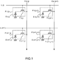
- the figure 1 schematically represents the detection area 10 of a matrix detector.
- This area includes a matrix of two rows and two columns to simplify understanding.
- Four pixels P are formed, each at the intersection of a row and a column. It is understood that the real matrices are generally much larger and have a large number of rows and columns.
- the pixel matrix belongs to a matrix detector 12 making it possible to produce digitized images.
- Each pixel P comprises a photosensitive zone, represented here by a photodiode D, and an electronic processing circuit formed, in the example of the figure 1 , by a single transistor T.
- the references of components D and T are followed by two coordinates specifying the rank of the row, respectively i and i + 1, and that of the column respectively j and j + 1.
- the pixels represented are also called pixel of type 1T because each having a transistor whose function will be described later.
- TFT thin-film field effect transistor
- the transistors of the TFT type can be based on metal oxides such as for example the transistors based on amorphous or crystalline oxide of indium, gallium and zinc known by their Anglo-Saxon abbreviation: IGZO.
- Other families of TFT type transistors can be implemented such as, for example, organic TFTs, TFTs made of amorphous silicon, TFTs made of polycrystalline silicon. In the latter type of TFT transistor, some have been synthesized at low temperature. They are known by their Anglo-Saxon abbreviation: LTPS for “Low-temperature polycrystalline silicon”.
- the invention is not limited to this type of transistors. It can for example be implemented for arrays comprising transistors based on complementary semiconductors made of crystalline silicon known in the Anglo-Saxon literature by their abbreviation CMOS for: "Complementary Metal Oxide Semiconductor”.
- the pixels P of the same column are connected to a column conductor Col. This conductor collects information from the pixels linked to it.
- the pixels P of the same line are connected to a line conductor L carrying a signal VG making it possible to control the corresponding line of pixels.
- the column conductor Col is used to collect information from a pixel in the corresponding column when it is selected by means of the signal VG.
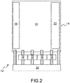
- the figure 2 schematically represents the detector 12 as a whole.
- the detector 12 comprises a slab 14 forming the substrate on which the components of the detection zone 10 are made.
- control modules 16 delivering control signals to all the line conductors L.
- the control modules 16 comprise for example shift registers making it possible to generate the control signals.
- the control modules 16 can be produced on a substrate separate from the slab 14.
- the production of the control modules 16 on the same substrate as the pixels P makes it possible to limit the connections connecting the slab 14 to its environment.
- the detector 12 includes reading circuits 18 connected to the column conductors Col.
- the read circuits 18 are, in turn, generally produced on substrates distinct from the slab 14.
- the read circuits 18 are connected to the slab 14 by means of plies.
- the detector 12 comprises a circuit 20 making it possible to control the control modules 16 and making it possible to recover the signals coming from the reading circuits 18, in particular for multiplexing them.
- the detector 12 comprises impedance modules 22 connected to each of the line conductors L.
- the impedance modules 22 are advantageously made on the slab 14 in order to limit the connections outside the slab 14.
- the invention is described in relation to a 1T type pixel matrix having only one conductor L per pixel line. It is also possible to implement the invention for matrices, in particular formed from 3T pixels, and having several control conductors per line of pixels. In this case, impedance modules can be associated with all the line conductors.
- the drive modules 16 To drive the read transistors T, the drive modules 16 generate binary signals, a high level of which allows the reading of a pixel line and a low level which does not allow the line to be read.
- the designations "high levels” and “low level” are purely arbitrary and are only used to distinguish the voltages applied to the line conductor. These names can of course be reversed.
- the control modules 16 use components of the transistor type and when the high level is applied to the line L, the latter has a lower impedance than when the low level is applied to line L. As indicated above, the highest impedance can cause local variations in potential on the line. These variations can be a source of disturbance in the image from detector 12.
- the impedance modules 22 are configured to lower the impedance of the line conductors L when the signals are transmitted at the low level. More precisely, for each line i, as long as the corresponding control module 16 transmits a line selection signal at the low level, the impedance module 22 maintains the corresponding line at low impedance.
- the impedance modules 22 are separate from the control modules.
- each line conductor L has two ends.
- the control modules 16 are connected to the line conductors L at a first end and the impedance modules 22 are connected to each of the line conductors L at a second end.
- the figure 3 illustrates this arrangement and its advantages. More specifically, the figure 3 represents a detector comprising 6 rows and 8 columns of pixels P. On the left part of the detection zone 10 where the pixels P are arranged, there are the control modules 16 and on the right part, the impedance modules 22. During the manufacture of the detector or during its use, line breaks L may appear.
- the cuts can be involuntary, in the event of a manufacturing defect, or intentional when the cut is used to repair a defect or to minimize its impact on the overall quality of the image from the detector 12.
- a first cut 24 appears on the first line between a control module 16 and the detection zone 10. Cut 26 and 28 appear inside the detection zone 10.
- the cut line portion opposite the control module 16 is electrically floating and its potential is not fixed.
- the potential of this floating portion can in turn disturb the potential of the adjacent rows, columns and pixels by capacitive coupling and therefore degrade the image quality from the detector.
- impedance modules 22 arranged on the opposite side to control modules 16 the isolated line portions of the control modules 16 are no longer floating and their potential is fixed at a value determined by the impedance modules 22, for example a value corresponding to an absence of line selection. This results in an improvement in the image quality from the detector by reducing the artifacts linked to the risk of coupling of these floating portions with neighboring elements, rows, columns or pixels. Consequently, the pixels of a cut line are either driven by the control module 16 associated with the line conductor or placed at low impedance by the impedance module 22 also associated with the line regardless of the position of the cut. along the line.
- the figure 2 represents the implementation of the invention in a detector comprising a slab 14 on which are integrated in addition to the pixels, the control modules 16, and the impedance modules 22.
- a level of integration requires the use of a same transistor technology both for the pixels P, for the control modules 16 and for the impedance modules 22.
- control modules 16 are not integrated on the slab 14.
- control modules 16 integrating the low-impedance maintenance for both signal levels VGon and VGoff using different transistor technologies.
- This variant is nevertheless of interest for stabilizing the impedance of broken lines, which frequently occurs in detectors having a large number of pixels.
- the impedance modules 22 are arranged on the opposite side from that occupied by the control modules 16.
- the impedance modules 22 can be located in the vicinity of the control modules 16, that is to say of the same side of the detection zone 10 and more precisely between control modules 16 and the detection zone 10.
- This arrangement has the advantage of grouping all the control and impedance components on the same edge of the detector 12.
- the advantage relating to maintaining the impedance of the cut lines disappears.
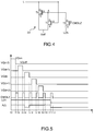
- the figure 4 shows an example of an impedance module 22 produced from three thin film transistors T1, T2 and T3.
- the drain of transistor T1 is connected to line L and its source to a voltage source Voff corresponding to the low level VGoff of the signal VG.
- the control module 16 applies to the line L the signal VG either at the high level VGon when the line L is selected, or at the low level VGoff when the line L is not selected.
- the control module 16, in particular when it is produced on the slab 14, can also use thin film transistors to apply the signal VG.
- the high level VGon is applied through a transistor placing the line L at low impedance while the low level VGoff is applied by blocking this same transistor placing the line L at high impedance.
- the impedance module 22 connects the line L to the voltage Voff when the line L is not selected, thus lowering the impedance of the line conductor L through the transistor T1.
- the transistors T2 and T3 allow the control of the transistor T1.
- the drains of the transistors T2 and T3 are connected to the gate of the transistor T1 forming a node A internal to the impedance module 22.
- the line L is connected to the gate of the transistor T2.
- the source of transistor T2 is connected to the voltage source Voff.
- the source of transistor T3 is connected to a command LZA making it possible to set the level of node A.
- the gate of transistor T3 is connected to a command CMDLZ making it possible to connect node A to the command LZA.
- the figure 5 illustrates in the form of a timing diagram the operation of the impedance module 22.
- the line selection signals VG of five consecutive lines from i-2 to i + 2 are shown.
- the signal VG (i-2) is at the high level VGon between the instants t0 and t1. After time t1, the signal VG (i-2) is at the low level VGoff.
- the selection of the following lines is then linked in the same way.
- the signal VG (i-1) is at the high level VGon between the instants t2 and t3.
- the signal VG (i) is at the high level VGon between the instants t4 and t5.
- the signal VG (i + 1) is at the high level VGon between the instants t6 and t7.
- the signal VG (i + 2) is at the high level VGon between instants t8 and t9.
- the signal CMDLZ goes high for a short time before the selection of each line L, in particular between the instants t3 and t4 for the line i.
- the signal LZA is at the high level.
- the signal LZA is at the low level.
- the line i When the line i is not selected, the node A remains in the high state, the transistor T1 is on and the impedance module 22 maintains at low impedance, the line conductor L (i) which remains at the voltage Voff.
- the voltage VGon is applied to the line conductor L (i) which makes the transistor T2 passing, causing the node A to drop to the low level.
- the transistor T1 becomes non-passing between the instants t4 and t5 .
- the impedance module 22 no longer changes the impedance of the line conductor L (i).
- the CMDLZ signal can be common to all lines and go up high before each line selection.
- the blocking of the transistor T1 of a line becomes effective only when the conductor of the line considered receives the signal VG in the high state.
- the signal LZA is kept low.
- the production on the same panel 14 of the pixels and of the two types of modules 16 and 22 is advantageously done by implementing a single transistor technology, in particular thin film TFT transistors.
- the TFT transistors implemented on a glass slab can hardly stand for a long time in the on state. This causes a drift in their threshold voltage and therefore premature aging of the detector. This is why, apart from the reading phase, the transistors are placed at the voltage Voff.
- the phase of reading all the detector's pixels occupies a period of the order of 1%, or even less, of the period of use of the detector. This ratio may be sufficient to avoid premature aging of the detector due to the switching of the TFT transistors.
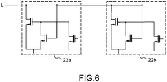
- the figure 6 shows an example where two impedance modules 22a and 22b are connected to the same line conductor L.
- the two modules 22a and 22b are used alternately.
- the module 22a is used during the reading of an image and the module 22b during the reading of the next image.
- This embodiment makes it possible to halve the durations during which the transistors are in the on state. The life of the detector is then increased in the same proportion.
- the impedance modules 22 represented on the figures 4 and 6 are well suited to being produced on the same TFT type slab as the detection zone 10. It is of course possible to implement the invention with other transistor technologies or to produce the detection zone 10 and the modules impedance 22 on different slabs.
- the impedance modules 22 can for example be produced by means of AND logic gates receiving the CMDLZ signal the VG signal and possibly the LZA signal.
- the output of the impedance modules 22 controlling the stopping of the low impedance of the corresponding line is obtained when the signal VG is at the high level and when the signal CMDLZ is at the low level.
- Other ways of making the impedance modules 22, such as by implementing shift registers, are of course possible.
Landscapes
- Engineering & Computer Science (AREA)
- Multimedia (AREA)
- Signal Processing (AREA)
- Solid State Image Pick-Up Elements (AREA)
- Measurement Of Radiation (AREA)
- Transforming Light Signals Into Electric Signals (AREA)
- Health & Medical Sciences (AREA)
- Toxicology (AREA)
- Investigating Or Analyzing Materials By The Use Of Electric Means (AREA)
Applications Claiming Priority (1)
| Application Number | Priority Date | Filing Date | Title |
|---|---|---|---|
| FR1873891A FR3091113B1 (fr) | 2018-12-21 | 2018-12-21 | Détecteur matriciel à conducteurs de ligne d’impédance maitrisée |
Publications (2)
| Publication Number | Publication Date |
|---|---|
| EP3672230A1 true EP3672230A1 (de) | 2020-06-24 |
| EP3672230B1 EP3672230B1 (de) | 2021-02-24 |
Family
ID=67107585
Family Applications (1)
| Application Number | Title | Priority Date | Filing Date |
|---|---|---|---|
| EP19218197.2A Active EP3672230B1 (de) | 2018-12-21 | 2019-12-19 | Matrixdetektor mit leitern mit gesteuerter impedanz |
Country Status (6)
| Country | Link |
|---|---|
| US (1) | US10999547B2 (de) |
| EP (1) | EP3672230B1 (de) |
| JP (1) | JP2020102847A (de) |
| KR (1) | KR20200078406A (de) |
| CN (1) | CN111355908A (de) |
| FR (1) | FR3091113B1 (de) |
Cited By (1)
| Publication number | Priority date | Publication date | Assignee | Title |
|---|---|---|---|---|
| FR3119708A1 (fr) | 2021-02-11 | 2022-08-12 | Trixell | Détecteur numérique à étages de conversion superposés |
Citations (4)
| Publication number | Priority date | Publication date | Assignee | Title |
|---|---|---|---|---|
| US20060001918A1 (en) * | 2004-07-01 | 2006-01-05 | Sony Corporation | Physical information acquisition method, a physical information acquisition apparatus, and a semiconductor device |
| US20070146514A1 (en) * | 2005-11-17 | 2007-06-28 | Noriya Maeda | Method of acquiring physical information and physical information acquiring device |
| US20120086826A1 (en) * | 2005-10-05 | 2012-04-12 | Panasonic Corporation | Solid-state imaging device, imaging apparatus and driving method for the same |
| WO2012152836A1 (fr) | 2011-05-10 | 2012-11-15 | Trixell S.A.S. | Dispositif d'adressage de lignes d'un circuit de commande pour matrice active de detection |
Family Cites Families (19)
| Publication number | Priority date | Publication date | Assignee | Title |
|---|---|---|---|---|
| US5619223A (en) * | 1994-04-14 | 1997-04-08 | Prime View Hk Limited | Apparatus for increasing the effective yield of displays with integregated row select driver circuit |
| EP0727083A1 (de) * | 1994-09-01 | 1996-08-21 | Koninklijke Philips Electronics N.V. | Flüssigkristallanzeigetafel |
| US6157375A (en) * | 1998-06-30 | 2000-12-05 | Sun Microsystems, Inc. | Method and apparatus for selective enabling of addressable display elements |
| US6809767B1 (en) * | 1999-03-16 | 2004-10-26 | Kozlowski Lester J | Low-noise CMOS active pixel sensor for imaging arrays with high speed global or row reset |
| EP1599854A1 (de) * | 2003-02-13 | 2005-11-30 | Koninklijke Philips Electronics N.V. | Optisch adressierbare matrixanzeige |
| FR2855326B1 (fr) * | 2003-05-23 | 2005-07-22 | Atmel Grenoble Sa | Capteur d'image matriciel en technologie cmos |
| JP4358125B2 (ja) * | 2005-02-04 | 2009-11-04 | 富士通マイクロエレクトロニクス株式会社 | クロストークノイズ低減回路を備えた半導体装置 |
| JP2006314025A (ja) * | 2005-05-09 | 2006-11-16 | Sony Corp | 撮像装置と撮像装置用の電源供給方法 |
| JP4192980B2 (ja) * | 2006-09-01 | 2008-12-10 | エプソンイメージングデバイス株式会社 | 電気光学装置、駆動回路および電子機器 |
| JP4349446B2 (ja) * | 2007-07-10 | 2009-10-21 | エプソンイメージングデバイス株式会社 | 電気光学装置、駆動回路および電子機器 |
| JP4673396B2 (ja) * | 2007-09-14 | 2011-04-20 | キヤノン株式会社 | 撮像装置及び撮像システム |
| FR2965440B1 (fr) * | 2010-09-29 | 2013-08-23 | Commissariat Energie Atomique | Dispositif d'imagerie a chute ohmique nulle dans un bus de donnee |
| JP2012129425A (ja) * | 2010-12-16 | 2012-07-05 | Canon Inc | マトリクス基板、検出装置、検出システム、及び、検出装置の駆動方法 |
| JP2013090139A (ja) * | 2011-10-18 | 2013-05-13 | Sony Corp | 撮像素子およびカメラシステム |
| TWI643500B (zh) * | 2014-03-31 | 2018-12-01 | 日商新力股份有限公司 | 攝像元件、攝像方法及電子機器 |
| JP2016042664A (ja) * | 2014-08-18 | 2016-03-31 | キヤノン株式会社 | センサアレー装置及びその制御方法、放射線撮影装置 |
| JP2018113615A (ja) * | 2017-01-12 | 2018-07-19 | ソニーセミコンダクタソリューションズ株式会社 | 固体撮像素子、駆動方法、および電子機器 |
| JP2018180414A (ja) * | 2017-04-19 | 2018-11-15 | 三菱電機株式会社 | 液晶表示装置 |
| US10873716B2 (en) * | 2018-11-05 | 2020-12-22 | SmartSens Technology (HK) Co., Ltd. | Dual row control signal circuit for reduced image sensor shading |
-
2018
- 2018-12-21 FR FR1873891A patent/FR3091113B1/fr not_active Expired - Fee Related
-
2019
- 2019-12-17 US US16/717,995 patent/US10999547B2/en active Active
- 2019-12-19 JP JP2019229018A patent/JP2020102847A/ja active Pending
- 2019-12-19 EP EP19218197.2A patent/EP3672230B1/de active Active
- 2019-12-20 KR KR1020190172401A patent/KR20200078406A/ko not_active Ceased
- 2019-12-23 CN CN201911334992.0A patent/CN111355908A/zh active Pending
Patent Citations (4)
| Publication number | Priority date | Publication date | Assignee | Title |
|---|---|---|---|---|
| US20060001918A1 (en) * | 2004-07-01 | 2006-01-05 | Sony Corporation | Physical information acquisition method, a physical information acquisition apparatus, and a semiconductor device |
| US20120086826A1 (en) * | 2005-10-05 | 2012-04-12 | Panasonic Corporation | Solid-state imaging device, imaging apparatus and driving method for the same |
| US20070146514A1 (en) * | 2005-11-17 | 2007-06-28 | Noriya Maeda | Method of acquiring physical information and physical information acquiring device |
| WO2012152836A1 (fr) | 2011-05-10 | 2012-11-15 | Trixell S.A.S. | Dispositif d'adressage de lignes d'un circuit de commande pour matrice active de detection |
Cited By (3)
| Publication number | Priority date | Publication date | Assignee | Title |
|---|---|---|---|---|
| FR3119708A1 (fr) | 2021-02-11 | 2022-08-12 | Trixell | Détecteur numérique à étages de conversion superposés |
| EP4043929A1 (de) | 2021-02-11 | 2022-08-17 | Trixell | Digitaler detektor mit überlagerten umwandlungsstufen |
| US12111429B2 (en) | 2021-02-11 | 2024-10-08 | Trixell | Digital detector with superposed conversion stages |
Also Published As
| Publication number | Publication date |
|---|---|
| US20200204754A1 (en) | 2020-06-25 |
| EP3672230B1 (de) | 2021-02-24 |
| CN111355908A (zh) | 2020-06-30 |
| KR20200078406A (ko) | 2020-07-01 |
| US10999547B2 (en) | 2021-05-04 |
| FR3091113B1 (fr) | 2021-03-05 |
| JP2020102847A (ja) | 2020-07-02 |
| FR3091113A1 (fr) | 2020-06-26 |
Similar Documents
| Publication | Publication Date | Title |
|---|---|---|
| RU2607732C2 (ru) | Устройство съемки изображений и система съемки изображений | |
| FR2487566A1 (fr) | Matrice de detection d'un rayonnement electromagnetique et intensificateur d'images radiologiques comportant une telle matrice | |
| US8223233B2 (en) | Imaging device and method of driving solid state imaging element | |
| WO2010015621A1 (fr) | Registre a decalage a transistors a effet de champ | |
| US9018590B2 (en) | Device for addressing lines of a control circuit for an active detection matrix | |
| US20100002113A1 (en) | Imaging device and method of driving solid state imaging element | |
| EP0064890A1 (de) | Einen Zeilenspeicher umfassende Einrichtung zur Bildabtastung in aufeinanderfolgenden Zeilen unter Verwendung elektrischer Ladungsübertragung und Fernsehkamera mit einer solchen Einrichtung | |
| JP7357297B2 (ja) | 撮像装置および撮像方法 | |
| EP3672230B1 (de) | Matrixdetektor mit leitern mit gesteuerter impedanz | |
| CA2539506C (fr) | Procede de commande d'un dispositif photosensible | |
| FR3091115A1 (fr) | Détecteur matriciel à regroupement rapide | |
| WO2014096433A1 (fr) | Procede de lecture d'un dispositif d'imagerie | |
| CA2378444C (fr) | Procede de commande d'un dispositif photosensible apte a produire des images de bonne qualite | |
| EP1425903B1 (de) | Steuerungsverfahren einer photoempfindlichen vorrichtung | |
| EP3026890B1 (de) | Steuerung der integrationszeit in einem lichtempfindlichen apparat | |
| EP3972240B1 (de) | Matrixdetektor mit mehreren gruppen von steuermodulen und ausführungsverfahren dieses detektors | |
| US20240357250A1 (en) | Imaging element and electronic device | |
| FR3071103B1 (fr) | Pixel photosensible et capteur d'image associe | |
| JP2017194280A (ja) | 撮像回路、信号読出回路、赤外線撮像装置、赤外線検出回路および撮像回路の動作方法 | |
| FR3145445A1 (fr) | Procédé de lecture et dispositif de lecture de signaux électriques issus d’un capteur photosensible | |
| FR2936087A1 (fr) | Registre a decalage a transistors a effet de champ. | |
| FR2660821A1 (fr) | Matrice photosensible a transfert de charges adaptee a un balayage progressif et son procede de fabrication. |
Legal Events
| Date | Code | Title | Description |
|---|---|---|---|
| PUAI | Public reference made under article 153(3) epc to a published international application that has entered the european phase |
Free format text: ORIGINAL CODE: 0009012 |
|
| STAA | Information on the status of an ep patent application or granted ep patent |
Free format text: STATUS: THE APPLICATION HAS BEEN PUBLISHED |
|
| AK | Designated contracting states |
Kind code of ref document: A1 Designated state(s): AL AT BE BG CH CY CZ DE DK EE ES FI FR GB GR HR HU IE IS IT LI LT LU LV MC MK MT NL NO PL PT RO RS SE SI SK SM TR |
|
| AX | Request for extension of the european patent |
Extension state: BA ME |
|
| STAA | Information on the status of an ep patent application or granted ep patent |
Free format text: STATUS: REQUEST FOR EXAMINATION WAS MADE |
|
| 17P | Request for examination filed |
Effective date: 20200916 |
|
| RBV | Designated contracting states (corrected) |
Designated state(s): AL AT BE BG CH CY CZ DE DK EE ES FI FR GB GR HR HU IE IS IT LI LT LU LV MC MK MT NL NO PL PT RO RS SE SI SK SM TR |
|
| GRAJ | Information related to disapproval of communication of intention to grant by the applicant or resumption of examination proceedings by the epo deleted |
Free format text: ORIGINAL CODE: EPIDOSDIGR1 |
|
| STAA | Information on the status of an ep patent application or granted ep patent |
Free format text: STATUS: GRANT OF PATENT IS INTENDED |
|
| RIC1 | Information provided on ipc code assigned before grant |
Ipc: H04N 5/376 20110101AFI20201016BHEP Ipc: H04N 5/378 20110101ALN20201016BHEP Ipc: H04N 5/32 20060101ALI20201016BHEP |
|
| GRAP | Despatch of communication of intention to grant a patent |
Free format text: ORIGINAL CODE: EPIDOSNIGR1 |
|
| RIC1 | Information provided on ipc code assigned before grant |
Ipc: H04N 5/376 20110101AFI20201026BHEP Ipc: H04N 5/32 20060101ALI20201026BHEP Ipc: H04N 5/378 20110101ALN20201026BHEP |
|
| INTG | Intention to grant announced |
Effective date: 20201202 |
|
| GRAS | Grant fee paid |
Free format text: ORIGINAL CODE: EPIDOSNIGR3 |
|
| GRAA | (expected) grant |
Free format text: ORIGINAL CODE: 0009210 |
|
| STAA | Information on the status of an ep patent application or granted ep patent |
Free format text: STATUS: THE PATENT HAS BEEN GRANTED |
|
| AK | Designated contracting states |
Kind code of ref document: B1 Designated state(s): AL AT BE BG CH CY CZ DE DK EE ES FI FR GB GR HR HU IE IS IT LI LT LU LV MC MK MT NL NO PL PT RO RS SE SI SK SM TR |
|
| REG | Reference to a national code |
Ref country code: CH Ref legal event code: EP |
|
| REG | Reference to a national code |
Ref country code: DE Ref legal event code: R096 Ref document number: 602019002796 Country of ref document: DE |
|
| REG | Reference to a national code |
Ref country code: AT Ref legal event code: REF Ref document number: 1365962 Country of ref document: AT Kind code of ref document: T Effective date: 20210315 |
|
| REG | Reference to a national code |
Ref country code: IE Ref legal event code: FG4D Free format text: LANGUAGE OF EP DOCUMENT: FRENCH |
|
| REG | Reference to a national code |
Ref country code: NL Ref legal event code: FP |
|
| REG | Reference to a national code |
Ref country code: LT Ref legal event code: MG9D |
|
| PG25 | Lapsed in a contracting state [announced via postgrant information from national office to epo] |
Ref country code: LT Free format text: LAPSE BECAUSE OF FAILURE TO SUBMIT A TRANSLATION OF THE DESCRIPTION OR TO PAY THE FEE WITHIN THE PRESCRIBED TIME-LIMIT Effective date: 20210224 Ref country code: PT Free format text: LAPSE BECAUSE OF FAILURE TO SUBMIT A TRANSLATION OF THE DESCRIPTION OR TO PAY THE FEE WITHIN THE PRESCRIBED TIME-LIMIT Effective date: 20210624 Ref country code: NO Free format text: LAPSE BECAUSE OF FAILURE TO SUBMIT A TRANSLATION OF THE DESCRIPTION OR TO PAY THE FEE WITHIN THE PRESCRIBED TIME-LIMIT Effective date: 20210524 Ref country code: HR Free format text: LAPSE BECAUSE OF FAILURE TO SUBMIT A TRANSLATION OF THE DESCRIPTION OR TO PAY THE FEE WITHIN THE PRESCRIBED TIME-LIMIT Effective date: 20210224 Ref country code: BG Free format text: LAPSE BECAUSE OF FAILURE TO SUBMIT A TRANSLATION OF THE DESCRIPTION OR TO PAY THE FEE WITHIN THE PRESCRIBED TIME-LIMIT Effective date: 20210524 Ref country code: FI Free format text: LAPSE BECAUSE OF FAILURE TO SUBMIT A TRANSLATION OF THE DESCRIPTION OR TO PAY THE FEE WITHIN THE PRESCRIBED TIME-LIMIT Effective date: 20210224 Ref country code: GR Free format text: LAPSE BECAUSE OF FAILURE TO SUBMIT A TRANSLATION OF THE DESCRIPTION OR TO PAY THE FEE WITHIN THE PRESCRIBED TIME-LIMIT Effective date: 20210525 |
|
| REG | Reference to a national code |
Ref country code: AT Ref legal event code: MK05 Ref document number: 1365962 Country of ref document: AT Kind code of ref document: T Effective date: 20210224 |
|
| PG25 | Lapsed in a contracting state [announced via postgrant information from national office to epo] |
Ref country code: LV Free format text: LAPSE BECAUSE OF FAILURE TO SUBMIT A TRANSLATION OF THE DESCRIPTION OR TO PAY THE FEE WITHIN THE PRESCRIBED TIME-LIMIT Effective date: 20210224 Ref country code: PL Free format text: LAPSE BECAUSE OF FAILURE TO SUBMIT A TRANSLATION OF THE DESCRIPTION OR TO PAY THE FEE WITHIN THE PRESCRIBED TIME-LIMIT Effective date: 20210224 Ref country code: RS Free format text: LAPSE BECAUSE OF FAILURE TO SUBMIT A TRANSLATION OF THE DESCRIPTION OR TO PAY THE FEE WITHIN THE PRESCRIBED TIME-LIMIT Effective date: 20210224 Ref country code: SE Free format text: LAPSE BECAUSE OF FAILURE TO SUBMIT A TRANSLATION OF THE DESCRIPTION OR TO PAY THE FEE WITHIN THE PRESCRIBED TIME-LIMIT Effective date: 20210224 |
|
| PG25 | Lapsed in a contracting state [announced via postgrant information from national office to epo] |
Ref country code: IS Free format text: LAPSE BECAUSE OF FAILURE TO SUBMIT A TRANSLATION OF THE DESCRIPTION OR TO PAY THE FEE WITHIN THE PRESCRIBED TIME-LIMIT Effective date: 20210624 |
|
| PG25 | Lapsed in a contracting state [announced via postgrant information from national office to epo] |
Ref country code: SM Free format text: LAPSE BECAUSE OF FAILURE TO SUBMIT A TRANSLATION OF THE DESCRIPTION OR TO PAY THE FEE WITHIN THE PRESCRIBED TIME-LIMIT Effective date: 20210224 Ref country code: AT Free format text: LAPSE BECAUSE OF FAILURE TO SUBMIT A TRANSLATION OF THE DESCRIPTION OR TO PAY THE FEE WITHIN THE PRESCRIBED TIME-LIMIT Effective date: 20210224 Ref country code: EE Free format text: LAPSE BECAUSE OF FAILURE TO SUBMIT A TRANSLATION OF THE DESCRIPTION OR TO PAY THE FEE WITHIN THE PRESCRIBED TIME-LIMIT Effective date: 20210224 Ref country code: CZ Free format text: LAPSE BECAUSE OF FAILURE TO SUBMIT A TRANSLATION OF THE DESCRIPTION OR TO PAY THE FEE WITHIN THE PRESCRIBED TIME-LIMIT Effective date: 20210224 |
|
| REG | Reference to a national code |
Ref country code: DE Ref legal event code: R097 Ref document number: 602019002796 Country of ref document: DE |
|
| PG25 | Lapsed in a contracting state [announced via postgrant information from national office to epo] |
Ref country code: DK Free format text: LAPSE BECAUSE OF FAILURE TO SUBMIT A TRANSLATION OF THE DESCRIPTION OR TO PAY THE FEE WITHIN THE PRESCRIBED TIME-LIMIT Effective date: 20210224 Ref country code: SK Free format text: LAPSE BECAUSE OF FAILURE TO SUBMIT A TRANSLATION OF THE DESCRIPTION OR TO PAY THE FEE WITHIN THE PRESCRIBED TIME-LIMIT Effective date: 20210224 Ref country code: RO Free format text: LAPSE BECAUSE OF FAILURE TO SUBMIT A TRANSLATION OF THE DESCRIPTION OR TO PAY THE FEE WITHIN THE PRESCRIBED TIME-LIMIT Effective date: 20210224 |
|
| PLBE | No opposition filed within time limit |
Free format text: ORIGINAL CODE: 0009261 |
|
| STAA | Information on the status of an ep patent application or granted ep patent |
Free format text: STATUS: NO OPPOSITION FILED WITHIN TIME LIMIT |
|
| PG25 | Lapsed in a contracting state [announced via postgrant information from national office to epo] |
Ref country code: ES Free format text: LAPSE BECAUSE OF FAILURE TO SUBMIT A TRANSLATION OF THE DESCRIPTION OR TO PAY THE FEE WITHIN THE PRESCRIBED TIME-LIMIT Effective date: 20210224 Ref country code: AL Free format text: LAPSE BECAUSE OF FAILURE TO SUBMIT A TRANSLATION OF THE DESCRIPTION OR TO PAY THE FEE WITHIN THE PRESCRIBED TIME-LIMIT Effective date: 20210224 |
|
| 26N | No opposition filed |
Effective date: 20211125 |
|
| PGFP | Annual fee paid to national office [announced via postgrant information from national office to epo] |
Ref country code: BE Payment date: 20211203 Year of fee payment: 3 |
|
| PG25 | Lapsed in a contracting state [announced via postgrant information from national office to epo] |
Ref country code: IT Free format text: LAPSE BECAUSE OF FAILURE TO SUBMIT A TRANSLATION OF THE DESCRIPTION OR TO PAY THE FEE WITHIN THE PRESCRIBED TIME-LIMIT Effective date: 20210224 |
|
| PG25 | Lapsed in a contracting state [announced via postgrant information from national office to epo] |
Ref country code: IS Free format text: LAPSE BECAUSE OF FAILURE TO SUBMIT A TRANSLATION OF THE DESCRIPTION OR TO PAY THE FEE WITHIN THE PRESCRIBED TIME-LIMIT Effective date: 20210624 |
|
| PG25 | Lapsed in a contracting state [announced via postgrant information from national office to epo] |
Ref country code: MC Free format text: LAPSE BECAUSE OF FAILURE TO SUBMIT A TRANSLATION OF THE DESCRIPTION OR TO PAY THE FEE WITHIN THE PRESCRIBED TIME-LIMIT Effective date: 20210224 |
|
| PG25 | Lapsed in a contracting state [announced via postgrant information from national office to epo] |
Ref country code: LU Free format text: LAPSE BECAUSE OF NON-PAYMENT OF DUE FEES Effective date: 20211219 Ref country code: IE Free format text: LAPSE BECAUSE OF NON-PAYMENT OF DUE FEES Effective date: 20211219 |
|
| REG | Reference to a national code |
Ref country code: DE Ref legal event code: R079 Ref document number: 602019002796 Country of ref document: DE Free format text: PREVIOUS MAIN CLASS: H04N0005376000 Ipc: H04N0025779000 |
|
| P01 | Opt-out of the competence of the unified patent court (upc) registered |
Effective date: 20230517 |
|
| PG25 | Lapsed in a contracting state [announced via postgrant information from national office to epo] |
Ref country code: CY Free format text: LAPSE BECAUSE OF FAILURE TO SUBMIT A TRANSLATION OF THE DESCRIPTION OR TO PAY THE FEE WITHIN THE PRESCRIBED TIME-LIMIT Effective date: 20210224 |
|
| PG25 | Lapsed in a contracting state [announced via postgrant information from national office to epo] |
Ref country code: HU Free format text: LAPSE BECAUSE OF FAILURE TO SUBMIT A TRANSLATION OF THE DESCRIPTION OR TO PAY THE FEE WITHIN THE PRESCRIBED TIME-LIMIT; INVALID AB INITIO Effective date: 20191219 |
|
| REG | Reference to a national code |
Ref country code: CH Ref legal event code: PL |
|
| REG | Reference to a national code |
Ref country code: NL Ref legal event code: MM Effective date: 20230101 |
|
| REG | Reference to a national code |
Ref country code: BE Ref legal event code: MM Effective date: 20221231 |
|
| PG25 | Lapsed in a contracting state [announced via postgrant information from national office to epo] |
Ref country code: SI Free format text: LAPSE BECAUSE OF FAILURE TO SUBMIT A TRANSLATION OF THE DESCRIPTION OR TO PAY THE FEE WITHIN THE PRESCRIBED TIME-LIMIT Effective date: 20210224 Ref country code: NL Free format text: LAPSE BECAUSE OF NON-PAYMENT OF DUE FEES Effective date: 20230101 |
|
| PG25 | Lapsed in a contracting state [announced via postgrant information from national office to epo] |
Ref country code: LI Free format text: LAPSE BECAUSE OF NON-PAYMENT OF DUE FEES Effective date: 20221231 Ref country code: CH Free format text: LAPSE BECAUSE OF NON-PAYMENT OF DUE FEES Effective date: 20221231 |
|
| PG25 | Lapsed in a contracting state [announced via postgrant information from national office to epo] |
Ref country code: BE Free format text: LAPSE BECAUSE OF NON-PAYMENT OF DUE FEES Effective date: 20221231 |
|
| PG25 | Lapsed in a contracting state [announced via postgrant information from national office to epo] |
Ref country code: MK Free format text: LAPSE BECAUSE OF FAILURE TO SUBMIT A TRANSLATION OF THE DESCRIPTION OR TO PAY THE FEE WITHIN THE PRESCRIBED TIME-LIMIT Effective date: 20210224 |
|
| GBPC | Gb: european patent ceased through non-payment of renewal fee |
Effective date: 20231219 |
|
| PG25 | Lapsed in a contracting state [announced via postgrant information from national office to epo] |
Ref country code: MT Free format text: LAPSE BECAUSE OF FAILURE TO SUBMIT A TRANSLATION OF THE DESCRIPTION OR TO PAY THE FEE WITHIN THE PRESCRIBED TIME-LIMIT Effective date: 20210224 |
|
| PG25 | Lapsed in a contracting state [announced via postgrant information from national office to epo] |
Ref country code: GB Free format text: LAPSE BECAUSE OF NON-PAYMENT OF DUE FEES Effective date: 20231219 |
|
| PG25 | Lapsed in a contracting state [announced via postgrant information from national office to epo] |
Ref country code: GB Free format text: LAPSE BECAUSE OF NON-PAYMENT OF DUE FEES Effective date: 20231219 |
|
| PG25 | Lapsed in a contracting state [announced via postgrant information from national office to epo] |
Ref country code: TR Free format text: LAPSE BECAUSE OF FAILURE TO SUBMIT A TRANSLATION OF THE DESCRIPTION OR TO PAY THE FEE WITHIN THE PRESCRIBED TIME-LIMIT Effective date: 20210224 |
|
| PGFP | Annual fee paid to national office [announced via postgrant information from national office to epo] |
Ref country code: DE Payment date: 20251119 Year of fee payment: 7 |
|
| PGFP | Annual fee paid to national office [announced via postgrant information from national office to epo] |
Ref country code: FR Payment date: 20251124 Year of fee payment: 7 |