EP3663368B1 - Tintenzusammensetzung und verfahren zur herstellung einer organischen lichtemittierenden vorrichtung - Google Patents
Tintenzusammensetzung und verfahren zur herstellung einer organischen lichtemittierenden vorrichtung Download PDFInfo
- Publication number
- EP3663368B1 EP3663368B1 EP19767490.6A EP19767490A EP3663368B1 EP 3663368 B1 EP3663368 B1 EP 3663368B1 EP 19767490 A EP19767490 A EP 19767490A EP 3663368 B1 EP3663368 B1 EP 3663368B1
- Authority
- EP
- European Patent Office
- Prior art keywords
- group
- substituted
- unsubstituted
- compound
- ink composition
- Prior art date
- Legal status (The legal status is an assumption and is not a legal conclusion. Google has not performed a legal analysis and makes no representation as to the accuracy of the status listed.)
- Active
Links
- FSWCCQWDVGZMRD-UHFFFAOYSA-N CC1CC=CCC1 Chemical compound CC1CC=CCC1 FSWCCQWDVGZMRD-UHFFFAOYSA-N 0.000 description 1
- UAEPNZWRGJTJPN-UHFFFAOYSA-N CC1CCCCC1 Chemical compound CC1CCCCC1 UAEPNZWRGJTJPN-UHFFFAOYSA-N 0.000 description 1
- ZUNSDEVCBWMHMO-UHFFFAOYSA-N COC(F)=C(F)F Chemical compound COC(F)=C(F)F ZUNSDEVCBWMHMO-UHFFFAOYSA-N 0.000 description 1
Images
Classifications
-
- C—CHEMISTRY; METALLURGY
- C09—DYES; PAINTS; POLISHES; NATURAL RESINS; ADHESIVES; COMPOSITIONS NOT OTHERWISE PROVIDED FOR; APPLICATIONS OF MATERIALS NOT OTHERWISE PROVIDED FOR
- C09D—COATING COMPOSITIONS, e.g. PAINTS, VARNISHES OR LACQUERS; FILLING PASTES; CHEMICAL PAINT OR INK REMOVERS; INKS; CORRECTING FLUIDS; WOODSTAINS; PASTES OR SOLIDS FOR COLOURING OR PRINTING; USE OF MATERIALS THEREFOR
- C09D11/00—Inks
- C09D11/30—Inkjet printing inks
- C09D11/32—Inkjet printing inks characterised by colouring agents
- C09D11/328—Inkjet printing inks characterised by colouring agents characterised by dyes
-
- C—CHEMISTRY; METALLURGY
- C07—ORGANIC CHEMISTRY
- C07C—ACYCLIC OR CARBOCYCLIC COMPOUNDS
- C07C211/00—Compounds containing amino groups bound to a carbon skeleton
- C07C211/43—Compounds containing amino groups bound to a carbon skeleton having amino groups bound to carbon atoms of six-membered aromatic rings of the carbon skeleton
- C07C211/57—Compounds containing amino groups bound to a carbon skeleton having amino groups bound to carbon atoms of six-membered aromatic rings of the carbon skeleton having amino groups bound to carbon atoms of six-membered aromatic rings being part of condensed ring systems of the carbon skeleton
- C07C211/61—Compounds containing amino groups bound to a carbon skeleton having amino groups bound to carbon atoms of six-membered aromatic rings of the carbon skeleton having amino groups bound to carbon atoms of six-membered aromatic rings being part of condensed ring systems of the carbon skeleton with at least one of the condensed ring systems formed by three or more rings
-
- C—CHEMISTRY; METALLURGY
- C07—ORGANIC CHEMISTRY
- C07C—ACYCLIC OR CARBOCYCLIC COMPOUNDS
- C07C217/00—Compounds containing amino and etherified hydroxy groups bound to the same carbon skeleton
- C07C217/78—Compounds containing amino and etherified hydroxy groups bound to the same carbon skeleton having amino groups and etherified hydroxy groups bound to carbon atoms of six-membered aromatic rings of the same carbon skeleton
- C07C217/94—Compounds containing amino and etherified hydroxy groups bound to the same carbon skeleton having amino groups and etherified hydroxy groups bound to carbon atoms of six-membered aromatic rings of the same carbon skeleton having amino groups bound to carbon atoms of six-membered aromatic rings being part of condensed ring systems and etherified hydroxy groups bound to carbon atoms of six-membered aromatic rings of the same carbon skeleton
-
- C—CHEMISTRY; METALLURGY
- C09—DYES; PAINTS; POLISHES; NATURAL RESINS; ADHESIVES; COMPOSITIONS NOT OTHERWISE PROVIDED FOR; APPLICATIONS OF MATERIALS NOT OTHERWISE PROVIDED FOR
- C09D—COATING COMPOSITIONS, e.g. PAINTS, VARNISHES OR LACQUERS; FILLING PASTES; CHEMICAL PAINT OR INK REMOVERS; INKS; CORRECTING FLUIDS; WOODSTAINS; PASTES OR SOLIDS FOR COLOURING OR PRINTING; USE OF MATERIALS THEREFOR
- C09D11/00—Inks
- C09D11/02—Printing inks
- C09D11/03—Printing inks characterised by features other than the chemical nature of the binder
- C09D11/033—Printing inks characterised by features other than the chemical nature of the binder characterised by the solvent
-
- C—CHEMISTRY; METALLURGY
- C09—DYES; PAINTS; POLISHES; NATURAL RESINS; ADHESIVES; COMPOSITIONS NOT OTHERWISE PROVIDED FOR; APPLICATIONS OF MATERIALS NOT OTHERWISE PROVIDED FOR
- C09D—COATING COMPOSITIONS, e.g. PAINTS, VARNISHES OR LACQUERS; FILLING PASTES; CHEMICAL PAINT OR INK REMOVERS; INKS; CORRECTING FLUIDS; WOODSTAINS; PASTES OR SOLIDS FOR COLOURING OR PRINTING; USE OF MATERIALS THEREFOR
- C09D11/00—Inks
- C09D11/02—Printing inks
- C09D11/03—Printing inks characterised by features other than the chemical nature of the binder
- C09D11/037—Printing inks characterised by features other than the chemical nature of the binder characterised by the pigment
-
- C—CHEMISTRY; METALLURGY
- C09—DYES; PAINTS; POLISHES; NATURAL RESINS; ADHESIVES; COMPOSITIONS NOT OTHERWISE PROVIDED FOR; APPLICATIONS OF MATERIALS NOT OTHERWISE PROVIDED FOR
- C09D—COATING COMPOSITIONS, e.g. PAINTS, VARNISHES OR LACQUERS; FILLING PASTES; CHEMICAL PAINT OR INK REMOVERS; INKS; CORRECTING FLUIDS; WOODSTAINS; PASTES OR SOLIDS FOR COLOURING OR PRINTING; USE OF MATERIALS THEREFOR
- C09D11/00—Inks
- C09D11/30—Inkjet printing inks
- C09D11/32—Inkjet printing inks characterised by colouring agents
- C09D11/322—Pigment inks
-
- C—CHEMISTRY; METALLURGY
- C09—DYES; PAINTS; POLISHES; NATURAL RESINS; ADHESIVES; COMPOSITIONS NOT OTHERWISE PROVIDED FOR; APPLICATIONS OF MATERIALS NOT OTHERWISE PROVIDED FOR
- C09D—COATING COMPOSITIONS, e.g. PAINTS, VARNISHES OR LACQUERS; FILLING PASTES; CHEMICAL PAINT OR INK REMOVERS; INKS; CORRECTING FLUIDS; WOODSTAINS; PASTES OR SOLIDS FOR COLOURING OR PRINTING; USE OF MATERIALS THEREFOR
- C09D11/00—Inks
- C09D11/30—Inkjet printing inks
- C09D11/36—Inkjet printing inks based on non-aqueous solvents
-
- C—CHEMISTRY; METALLURGY
- C09—DYES; PAINTS; POLISHES; NATURAL RESINS; ADHESIVES; COMPOSITIONS NOT OTHERWISE PROVIDED FOR; APPLICATIONS OF MATERIALS NOT OTHERWISE PROVIDED FOR
- C09D—COATING COMPOSITIONS, e.g. PAINTS, VARNISHES OR LACQUERS; FILLING PASTES; CHEMICAL PAINT OR INK REMOVERS; INKS; CORRECTING FLUIDS; WOODSTAINS; PASTES OR SOLIDS FOR COLOURING OR PRINTING; USE OF MATERIALS THEREFOR
- C09D11/00—Inks
- C09D11/30—Inkjet printing inks
- C09D11/38—Inkjet printing inks characterised by non-macromolecular additives other than solvents, pigments or dyes
-
- C—CHEMISTRY; METALLURGY
- C09—DYES; PAINTS; POLISHES; NATURAL RESINS; ADHESIVES; COMPOSITIONS NOT OTHERWISE PROVIDED FOR; APPLICATIONS OF MATERIALS NOT OTHERWISE PROVIDED FOR
- C09D—COATING COMPOSITIONS, e.g. PAINTS, VARNISHES OR LACQUERS; FILLING PASTES; CHEMICAL PAINT OR INK REMOVERS; INKS; CORRECTING FLUIDS; WOODSTAINS; PASTES OR SOLIDS FOR COLOURING OR PRINTING; USE OF MATERIALS THEREFOR
- C09D11/00—Inks
- C09D11/50—Sympathetic, colour changing or similar inks
-
- C—CHEMISTRY; METALLURGY
- C09—DYES; PAINTS; POLISHES; NATURAL RESINS; ADHESIVES; COMPOSITIONS NOT OTHERWISE PROVIDED FOR; APPLICATIONS OF MATERIALS NOT OTHERWISE PROVIDED FOR
- C09K—MATERIALS FOR MISCELLANEOUS APPLICATIONS, NOT PROVIDED FOR ELSEWHERE
- C09K11/00—Luminescent materials, e.g. electroluminescent or chemiluminescent
- C09K11/06—Luminescent materials, e.g. electroluminescent or chemiluminescent containing organic luminescent materials
-
- H—ELECTRICITY
- H10—SEMICONDUCTOR DEVICES; ELECTRIC SOLID-STATE DEVICES NOT OTHERWISE PROVIDED FOR
- H10K—ORGANIC ELECTRIC SOLID-STATE DEVICES
- H10K71/00—Manufacture or treatment specially adapted for the organic devices covered by this subclass
- H10K71/10—Deposition of organic active material
- H10K71/12—Deposition of organic active material using liquid deposition, e.g. spin coating
- H10K71/15—Deposition of organic active material using liquid deposition, e.g. spin coating characterised by the solvent used
-
- H—ELECTRICITY
- H10—SEMICONDUCTOR DEVICES; ELECTRIC SOLID-STATE DEVICES NOT OTHERWISE PROVIDED FOR
- H10K—ORGANIC ELECTRIC SOLID-STATE DEVICES
- H10K85/00—Organic materials used in the body or electrodes of devices covered by this subclass
- H10K85/60—Organic compounds having low molecular weight
- H10K85/631—Amine compounds having at least two aryl rest on at least one amine-nitrogen atom, e.g. triphenylamine
- H10K85/633—Amine compounds having at least two aryl rest on at least one amine-nitrogen atom, e.g. triphenylamine comprising polycyclic condensed aromatic hydrocarbons as substituents on the nitrogen atom
-
- C—CHEMISTRY; METALLURGY
- C07—ORGANIC CHEMISTRY
- C07C—ACYCLIC OR CARBOCYCLIC COMPOUNDS
- C07C2603/00—Systems containing at least three condensed rings
- C07C2603/02—Ortho- or ortho- and peri-condensed systems
- C07C2603/04—Ortho- or ortho- and peri-condensed systems containing three rings
- C07C2603/06—Ortho- or ortho- and peri-condensed systems containing three rings containing at least one ring with less than six ring members
- C07C2603/10—Ortho- or ortho- and peri-condensed systems containing three rings containing at least one ring with less than six ring members containing five-membered rings
- C07C2603/12—Ortho- or ortho- and peri-condensed systems containing three rings containing at least one ring with less than six ring members containing five-membered rings only one five-membered ring
- C07C2603/18—Fluorenes; Hydrogenated fluorenes
-
- C—CHEMISTRY; METALLURGY
- C09—DYES; PAINTS; POLISHES; NATURAL RESINS; ADHESIVES; COMPOSITIONS NOT OTHERWISE PROVIDED FOR; APPLICATIONS OF MATERIALS NOT OTHERWISE PROVIDED FOR
- C09K—MATERIALS FOR MISCELLANEOUS APPLICATIONS, NOT PROVIDED FOR ELSEWHERE
- C09K2211/00—Chemical nature of organic luminescent or tenebrescent compounds
- C09K2211/10—Non-macromolecular compounds
- C09K2211/1003—Carbocyclic compounds
- C09K2211/1007—Non-condensed systems
-
- C—CHEMISTRY; METALLURGY
- C09—DYES; PAINTS; POLISHES; NATURAL RESINS; ADHESIVES; COMPOSITIONS NOT OTHERWISE PROVIDED FOR; APPLICATIONS OF MATERIALS NOT OTHERWISE PROVIDED FOR
- C09K—MATERIALS FOR MISCELLANEOUS APPLICATIONS, NOT PROVIDED FOR ELSEWHERE
- C09K2211/00—Chemical nature of organic luminescent or tenebrescent compounds
- C09K2211/10—Non-macromolecular compounds
- C09K2211/1003—Carbocyclic compounds
- C09K2211/1011—Condensed systems
-
- C—CHEMISTRY; METALLURGY
- C09—DYES; PAINTS; POLISHES; NATURAL RESINS; ADHESIVES; COMPOSITIONS NOT OTHERWISE PROVIDED FOR; APPLICATIONS OF MATERIALS NOT OTHERWISE PROVIDED FOR
- C09K—MATERIALS FOR MISCELLANEOUS APPLICATIONS, NOT PROVIDED FOR ELSEWHERE
- C09K2211/00—Chemical nature of organic luminescent or tenebrescent compounds
- C09K2211/10—Non-macromolecular compounds
- C09K2211/1003—Carbocyclic compounds
- C09K2211/1014—Carbocyclic compounds bridged by heteroatoms, e.g. N, P, Si or B
-
- H—ELECTRICITY
- H10—SEMICONDUCTOR DEVICES; ELECTRIC SOLID-STATE DEVICES NOT OTHERWISE PROVIDED FOR
- H10K—ORGANIC ELECTRIC SOLID-STATE DEVICES
- H10K50/00—Organic light-emitting devices
- H10K50/10—OLEDs or polymer light-emitting diodes [PLED]
- H10K50/11—OLEDs or polymer light-emitting diodes [PLED] characterised by the electroluminescent [EL] layers
-
- H—ELECTRICITY
- H10—SEMICONDUCTOR DEVICES; ELECTRIC SOLID-STATE DEVICES NOT OTHERWISE PROVIDED FOR
- H10K—ORGANIC ELECTRIC SOLID-STATE DEVICES
- H10K50/00—Organic light-emitting devices
- H10K50/10—OLEDs or polymer light-emitting diodes [PLED]
- H10K50/14—Carrier transporting layers
- H10K50/15—Hole transporting layers
-
- H—ELECTRICITY
- H10—SEMICONDUCTOR DEVICES; ELECTRIC SOLID-STATE DEVICES NOT OTHERWISE PROVIDED FOR
- H10K—ORGANIC ELECTRIC SOLID-STATE DEVICES
- H10K50/00—Organic light-emitting devices
- H10K50/10—OLEDs or polymer light-emitting diodes [PLED]
- H10K50/14—Carrier transporting layers
- H10K50/16—Electron transporting layers
-
- H—ELECTRICITY
- H10—SEMICONDUCTOR DEVICES; ELECTRIC SOLID-STATE DEVICES NOT OTHERWISE PROVIDED FOR
- H10K—ORGANIC ELECTRIC SOLID-STATE DEVICES
- H10K50/00—Organic light-emitting devices
- H10K50/10—OLEDs or polymer light-emitting diodes [PLED]
- H10K50/17—Carrier injection layers
-
- H—ELECTRICITY
- H10—SEMICONDUCTOR DEVICES; ELECTRIC SOLID-STATE DEVICES NOT OTHERWISE PROVIDED FOR
- H10K—ORGANIC ELECTRIC SOLID-STATE DEVICES
- H10K50/00—Organic light-emitting devices
- H10K50/10—OLEDs or polymer light-emitting diodes [PLED]
- H10K50/17—Carrier injection layers
- H10K50/171—Electron injection layers
-
- H—ELECTRICITY
- H10—SEMICONDUCTOR DEVICES; ELECTRIC SOLID-STATE DEVICES NOT OTHERWISE PROVIDED FOR
- H10K—ORGANIC ELECTRIC SOLID-STATE DEVICES
- H10K71/00—Manufacture or treatment specially adapted for the organic devices covered by this subclass
- H10K71/10—Deposition of organic active material
- H10K71/12—Deposition of organic active material using liquid deposition, e.g. spin coating
- H10K71/13—Deposition of organic active material using liquid deposition, e.g. spin coating using printing techniques, e.g. ink-jet printing or screen printing
- H10K71/135—Deposition of organic active material using liquid deposition, e.g. spin coating using printing techniques, e.g. ink-jet printing or screen printing using ink-jet printing
-
- H—ELECTRICITY
- H10—SEMICONDUCTOR DEVICES; ELECTRIC SOLID-STATE DEVICES NOT OTHERWISE PROVIDED FOR
- H10K—ORGANIC ELECTRIC SOLID-STATE DEVICES
- H10K85/00—Organic materials used in the body or electrodes of devices covered by this subclass
- H10K85/60—Organic compounds having low molecular weight
- H10K85/615—Polycyclic condensed aromatic hydrocarbons, e.g. anthracene
- H10K85/626—Polycyclic condensed aromatic hydrocarbons, e.g. anthracene containing more than one polycyclic condensed aromatic rings, e.g. bis-anthracene
Definitions
- the present specification relates to an ink composition and a method for manufacturing an organic light emitting device.
- a deposition process in the related art has a disadvantage in that it is difficult to manufacture a red-green-blue (RGB) type OLED display because a mask sagging phenomenon occurs as the area of the display increases.
- a solution process such as inkjet printing has an advantage in that a RGB type pattern may be formed even in a large area of a display, and all RGBs may be formed with a one-time process only.
- An ink composition used in an inkjet printing process needs to enable a stable discharge, prevent a functional layer material such as a charge transport material or a light emitting material and a solvent from being phase-separated, and enable a uniform film to be formed during the formation of the film.
- solvents of ethers having a relatively low polarity or solvents of hydrocarbons have been frequently used in the ink composition, and for example, solvents such as phenoxytoluene and cyclohexylbenzene have been used.
- solvents such as phenoxytoluene and cyclohexylbenzene have been used.
- the solvent is used as a main solvent, there are problems in that the process time is prolonged because there is a limitation in increasing the solid content of ink due to the low solubility for the functional layer material, , and a stable film cannot be formed because the phase separation occurs during the drying.
- the solubility of a solvent for a functional layer material is low, the number of drops dropped onto a pixel is increased in order to obtain a desired thickness because the amount of functional layer material which may be dissolved in ink is limited, so that it is difficult not only to obtain a flat profile, but also to obtain a desired thickness.
- a solvent used in an ink composition needs to have high solubility for a functional layer material and have a high boiling point in order to prevent a problem in that a nozzle part is dried.
- cyclohexanone in the related art corresponds to a solvent having good solubility, but has a low boiling point, so that when cyclohexanone is used in an ink composition, cyclohexanone is not appropriate for an inkjet process because a nozzle part is dried.
- the present specification has been made in an effort to provide an ink composition that may be used in an organic light emitting device and a method for manufacturing an organic light emitting device using the same.
- the present specification provides an ink composition including: a compound represented by the following Formula 1; and a solvent represented by the following Formula 2.
- L1, L2, and L4 are the same as or different from each other, and are each independently a direct bond; a substituted or unsubstituted alkylene group; a substituted or unsubstituted arylene group; or a substituted or unsubstituted heteroarylene group
- L3 is a substituted or unsubstituted arylene group; or a substituted or unsubstituted heteroarylene group
- X1 and X2 are the same as or different from each other, and are each independently a photocurable group or a thermosetting group
- Ar1 and Ar2 are the same as or different from each other, and are each independently a substituted or unsubstituted aryl group; or a substituted or unsubstituted heteroaryl group
- R1 to R6 are the same as or different from each other, and are each independently hydrogen; deuterium; a substituted or unsubstituted alkyl group; a substituted or unsubstituted
- the present specification provides a method for manufacturing an organic light emitting device, the method including: preparing a substrate; forming a first electrode or a second electron on the substrate; forming an organic material layer having one or more layers on the first electrode or the second electrode; and forming a second electrode or a first electrode on the organic material layer, in which the forming of the organic material layer includes forming an organic material layer having one or more layers by using the ink composition.
- the solubility of a solvent for a functional layer material is high, so that it is possible to increase the content of the functional layer material in the ink composition and to enhance the stability of the ink composition due to the increase in content of the functional layer material in the ink composition. That is, a flat film may be formed because precipitation or phase separation of the functional layer material does not occur.
- a uniform film may be formed by controlling the evaporation rate in the process of drying the ink composition due to low vapor pressure characteristics.
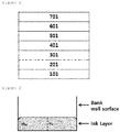
- FIG. 1 illustrates an example of an organic light emitting device according to an exemplary embodiment of the present specification.
- An ink composition used in an inkjet printing process needs to enable a stable discharge, prevent a functional layer material such as a charge transport material or a light emitting material and a solvent from being phase-separated, and enable a uniform film to be formed during the formation of the film.
- solvents of ethers having a relatively low polarity and solvents of hydrocarbons have been frequently used in the ink composition, and for example, solvents such as phenoxytoluene and cyclohexylbenzene have been used.
- solvents such as phenoxytoluene and cyclohexylbenzene have been used.
- the solvent is used as a main solvent, there are problems in that the process time is prolonged due to the limitation because there is a limitation in increasing the solid content of ink due to the low solubility for the functional layer material,, and a stable film cannot be formed because the phase separation occurs during the drying.
- the solubility of a solvent for a functional layer material is low, the number of drops dropped onto a pixel is increased in order to obtain a desired thickness because the amount of functional layer material which may be dissolved in ink is limited, so that it is difficult not only to obtain a flat profile, but also to obtain a desired thickness.
- a solvent used in an ink composition needs to have high solubility for a functional layer material and have a high boiling point in order to prevent a problem in that a nozzle part is dried.
- cyclohexanone in the related art corresponds to a solvent having good solubility, but has a low boiling point, so that when cyclohexanone is used in an ink composition, cyclohexanone is not appropriate for an inkjet process because a nozzle part is dried.
- the solubility of a solvent for a functional layer material is high, so that it is possible to increase the content of the functional layer material in the ink composition and to enhance the stability of the ink composition due to the increase in content of the functional layer material in the ink composition. That is, a flat film may be formed because precipitation or phase separation of the functional layer material does not occur.
- a uniform film may be formed by controlling the evaporation rate in the process of drying the ink composition due to low vapor pressure characteristics.
- an arylamine-based single molecule used in an organic light emitting device for a solution process does not itself have resistance to a solvent in the next process, a curing group needs to be introduced into the arylamine-based single molecule which can be used in OLED device for a solution process.
- a fluorene-based compound to which an amine group is bonded which is represented by Formula 1 of the present specification, may reduce steric hindrance around a curing group as an appropriate distance is maintained between the curing group and fluorene due to a linker. Accordingly, the mobility of the curing group itself may be increased to efficiently perform a curing reaction during light and heat treatments on a thin film, and to form a thin film having excellent solvent resistance.
- a styrene group or an ethenyl group as a curing agent is bonded to the fluorene-based compound according to an exemplary embodiment of the present specification, it is possible to reduce the interference with the interaction on a thin film in a part which is connected to a fluorene to which a cured product is bonded and an arylamine-based single molecular core skeleton by introducing a curing group into the position of No. 9 carbon of fluorene in which the conjugation with the core structure of fluorene is broken. In addition, it is possible not only to minimize an undesirable effect on the molecular orbital function of the core skeleton, but also to manufacture an organic light emitting device having a longer service life.
- the solvent represented by Formula 2 has higher solubility and a higher boiling point than solvents in the related art, so that it is possible to increase the content of the compound represented by Formula 1, which is a functional layer material in the ink composition. Accordingly, since the stability of the ink composition may be enhanced, precipitation or phase separation of the functional layer material does not occur, so that it possible to effectively form a flat film.
- substitution means that a hydrogen atom bonded to a carbon atom of a compound is changed into another substituent, and a position to be substituted is not limited as long as the position is a position at which the hydrogen atom is substituted, that is, a position at which the substituent may be substituted, and when two or more are substituted, the two or more substituents may be the same as or different from each other.
- substituted or unsubstituted means being substituted with one or two or more substituents selected from the group consisting of deuterium; a halogen group; a nitrile group; a nitro group; a hydroxyl group; an alkoxy group; a silyl group; an alkyl group; a cycloalkyl group; an amine group; an aryl group; and a heterocyclic group including one or more of N, O, S, Se, and Si atoms, being substituted with a substituent to which two or more substituents among the substituents exemplified above are linked, or having no substituent.
- examples of a halogen group include fluorine, chlorine, bromine or iodine.
- an alkyl group may be straight-chained or branch-chained, and the number of carbon atoms thereof is not particularly limited, but is preferably 1 to 50, and more preferably 1 to 30.
- Specific examples thereof include methyl, ethyl, propyl, n-propyl, isopropyl, butyl, n-butyl, isobutyl, tert-butyl, sec-butyl, 1-methyl-butyl, 1-ethyl-butyl, pentyl, n-pentyl, isopentyl, neopentyl, tert-pentyl, hexyl, n-hexyl, 1-methylpentyl, 2-methylpentyl, 4-methyl-2-pentyl, 3,3-dimethylbutyl, 2-ethylbutyl, heptyl, n-heptyl, 1-methylhexyl, cyclopentylmethyl, cyclopent
- a cycloalkyl group is not particularly limited, but has preferably 3 to 60 carbon atoms, and more preferably 3 to 30 carbon atoms.
- Specific examples thereof include cyclopropyl, cyclobutyl, cyclopentyl, 3-methylcyclopentyl, 2,3-dimethylcyclopentyl, cyclohexyl, 3-methylcyclohexyl, 4-methylcyclohexyl, 2,3-dimethylcyclohexyl, 3,4,5-trimethylcyclohexyl, 4-tert-butylcyclohexyl, cycloheptyl, cyclooctyl, and the like, but are not limited thereto.
- an alkoxy group may be straight-chained, branched, or cyclic.
- the carbon number of the alkoxy group is not particularly limited, but is preferably1 to 20 carbon atoms, and more preferably 1 to 10 carbon atoms.
- Specific examples thereof include methoxy, ethoxy, n-propoxy, isopropoxy, i-propyloxy, n-butoxy, isobutoxy, tert-butoxy, sec-butoxy, n-pentyloxy, neopentyloxy, isopentyloxy, n-hexyloxy, 3,3-dimethylbutyloxy, 2-ethylbutyloxy, n-octyloxy, n-nonyloxy, n-decyloxy, benzyloxy, p-methylbenzyloxy, and the like, but are not limited thereto.
- a silyl group includes Si and is a substituent to which the Si atom is directly linked as a radical, and is represented by -SiR 201 R 202 R 203 , and R 201 to R 203 are the same as or different from each other, and may be each independently a substituent composed of at least one of hydrogen; deuterium; a halogen group; an alkyl group; an alkenyl group; an alkoxy group; a cycloalkyl group; an aryl group; and a heterocyclic group.
- silyl group examples include a trimethylsilyl group, a triethylsilyl group, a t-butyldimethylsilyl group, a vinyldimethylsilyl group, a propyldimethylsilyl group, a triphenylsilyl group, a diphenylsilyl group, a phenylsilyl group, and the like, but are not limited thereto.
- an aryl group is a monocyclic aryl group
- the number of carbon atoms thereof is not particularly limited, but is preferably 6 to 50, and more preferably 6 to 30.
- Specific examples of the monocyclic aryl group include a phenyl group, a biphenyl group, a terphenyl group, a quarterphenyl group, and the like, but are not limited thereto.
- the aryl group is a polycyclic aryl group
- the number of carbon atoms thereof is not particularly limited, but is preferably 10 to 50, and more preferably 10 to 30.
- Specific examples of the polycyclic aryl group include a naphthyl group, an anthracenyl group, a phenanthryl group, pyrenyl group, a perylenyl group, a triphenylene group, a chrysenyl group, a fluorenyl group, and the like, but are not limited thereto.
- the fluorenyl group may be substituted, and adjacent substituents may be bonded to each other to form a ring.
- the substituent may be and the like, but is not limited thereto.
- a heterocyclic group includes one or more of N, O, S, Si, and Se as a heteroatom, and the number of carbon atoms thereof is not particularly limited, but is preferably 2 to 60, and more preferably 2 to 30.
- the heterocyclic group include a thiophene group, a furan group, a pyrrole group, an imidazole group, a thiazole group, an oxazole group, an oxadiazole group, a triazole group, a pyridine group, a bipyridine group, a pyrimidine group, a triazine group, an acridine group, a pyridazine group, a pyrazine group, a quinoline group, a quinazoline group, a quinoxaline group, a phthalazine group, a pteridine group, a pyrido pyrimidine group, a pyrido pyrazine
- a heteroaryl group may be selected from the examples of the heterocyclic group except for an aromatic heteroaryl group, but is not limited thereto.
- an amine group is represented by -NR 206 R 207 , and R 206 and R 207 are the same as or different from each other, and may be each independently a substituent composed of at least one of hydrogen, deuterium, a halogen group, an alkyl group, an alkenyl group, an alkoxy group, a cycloalkyl group, an aryl group, and a heterocyclic group.
- the amine group may be selected from the group consisting of -NH 2 , a monoalkylamine group, a dialkylamine group, an N-alkylarylamine group, a monoarylamine group, a diarylamine group, an N-arylheteroarylamine group, an N-alkylheteroarylamine group, a monoheteroarylamine group, and a diheteroarylamine group, and the number of carbon atoms thereof is not particularly limited, but is preferably 1 to 30, and more preferably 1 to 20.
- the amine group include a methylamine group, a dimethylamine group, an ethylamine group, a diethylamine group, a phenylamine group, a naphthylamine group, a biphenylamine group, an anthracenylamine group, a 9-methyl-anthracenylamine group, a diphenylamine group, a ditolylamine group, an N-phenyltolylamine group, a triphenylamine group, an N-phenylbiphenylamine group, an N-phenylnaphthylamine group, an N-biphenylnaphthylamine group; an N-naphthylfluorenylamine group; an N-phenylphenanthrenylamine group, an N-biphenylphenanthrenylamine group, an N-phenylfluorenylamine group, an N-phenyl terphenylamine group
- examples of an arylamine group include a substituted or unsubstituted monoarylamine group, a substituted or unsubstituted diarylamine group, or a substituted or unsubstituted triarylamine group.
- the aryl group in the arylamine group may be a monocyclic aryl group or a polycyclic aryl group.
- the arylamine group including two or more aryl groups may include a monocyclic aryl group, a polycyclic aryl group, or both a monocyclic aryl group and a polycyclic aryl group.
- the aryl group in the arylamine group may be selected from the above-described examples of the aryl group.
- an alkylene group means a group having two bonding positions in an alkyl group, that is, a divalent group.
- the above-described description on the alkyl group may be applied to the alkylene group, except for a divalent alkylene group.
- an arylene group means a group having two bonding positions in an aryl group, that is, a divalent group.
- the above-described description on the aryl group may be applied to the arylene group, except for a divalent arylene group.
- a heteroarylene group means a group having two bonding positions in a heteroaryl group, that is, a divalent group.
- the above-described description on the heteroaryl group may be applied to the heteroarylene group, except for a divalent heteroarylene group.
- L1, L2, and L4 are the same as or different from each other, and are each independently a direct bond; a substituted or unsubstituted alkylene group; a substituted or unsubstituted arylene group; or a substituted or unsubstituted heteroarylene group.
- L1 is a direct bond.
- L2 is a direct bond.
- L1 and L2 are the same as or different from each other, and are each independently a substituted or unsubstituted alkylene group having 1 to 20 carbon atoms.
- L1 and L2 are the same as or different from each other, and are each independently a substituted or unsubstituted alkylene group having 1 to 10 carbon atoms.
- L1 is a substituted or unsubstituted hexylene group, a substituted or unsubstituted heptylene group, or a substituted or unsubstituted octylene group.
- L1 is a hexylene group.
- L1 is a heptylene group.
- L1 is an octylene group.
- L2 is a substituted or unsubstituted hexylene group, a substituted or unsubstituted heptylene group, or a substituted or unsubstituted octylene group.
- L2 is a hexylene group.
- L2 is a heptylene group.
- L2 is an octylene group.
- L4 is a direct bond.
- L4 is a substituted or unsubstituted alkylene group having 1 to 10 carbon atoms.
- L4 is a substituted or unsubstituted methylene group, a substituted or unsubstituted ethylene group, a substituted or unsubstituted propylene group, a substituted or unsubstituted butylene group, a substituted or unsubstituted pentylene group, or a substituted or unsubstituted hexylene group.
- L4 is a methylene group.
- L4 is an ethylene group.
- L3 is a substituted or unsubstituted arylene group; or a substituted or unsubstituted heteroarylene group.
- L3 is a substituted or unsubstituted arylene group having 6 to 30 carbon atoms.
- L3 is a substituted or unsubstituted phenylene group, a substituted or unsubstituted biphenylene group, a substituted or unsubstituted terphenylene group; a substituted or unsubstituted naphthylene group, a substituted or unsubstituted phenanthrylene group, a substituted or unsubstituted triphenylene group, or a substituted or unsubstituted fluorenylene group.
- L3 is a biphenylene group.
- L3 is a substituted or unsubstituted heteroarylene group having 2 to 30 carbon atoms.
- X1 and X2 are the same as or different from each other, and are each independently a photocurable group or a thermosetting group.
- X1 and X2 are any one selected from the following structures.
- a 1 to A 3 are the same as or different from each other, and are each independently a substituted or unsubstituted alkyl group having 1 to 6 carbon atoms.
- Ar1 and Ar2 are the same as or different from each other, and are each independently a substituted or unsubstituted aryl group; or a substituted or unsubstituted heteroaryl group.
- Ar1 and Ar2 are the same as or different from each other, and are each independently a substituted or unsubstituted aryl group having 6 to 30 carbon atoms.
- Ar1 is a substituted or unsubstituted phenyl group, a substituted or unsubstituted biphenyl group, a substituted or unsubstituted terphenyl group, a substituted or unsubstituted naphthyl group, a substituted or unsubstituted phenanthryl group, a substituted or unsubstituted triphenylene group, or a substituted or unsubstituted fluorenyl group.
- Ar1 is a phenyl group.
- Ar1 is a biphenyl group.
- Ar1 is a naphthyl group.
- Ar2 is a substituted or unsubstituted phenyl group, a substituted or unsubstituted biphenyl group, a substituted or unsubstituted terphenyl group, a substituted or unsubstituted naphthyl group, a substituted or unsubstituted phenanthryl group, a substituted or unsubstituted triphenylene group, or a substituted or unsubstituted fluorenyl group.
- Ar2 is a phenyl group.
- Ar2 is a biphenyl group.
- Ar2 is a naphthyl group.
- R1 to R6 are the same as or different from each other, and are each independently hydrogen; deuterium; a substituted or unsubstituted alkyl group; a substituted or unsubstituted alkoxy group; a substituted or unsubstituted aryl group; or a substituted or unsubstituted heteroaryl group.
- R1 to R6 are the same as or different from each other, and are each independently a substituted or unsubstituted alkyl group having 1 to 10 carbon atoms.
- R1 to R6 are the same as or different from each other, and are each independently a substituted or unsubstituted methyl group, a substituted or unsubstituted ethyl group, a substituted or unsubstituted propyl group, a substituted or unsubstituted isopropyl group, or a substituted or unsubstituted tert-butyl group.
- R1 is a methyl group.
- R4 is a methyl group.
- R1 to R6 are each hydrogen.
- R11 is hydrogen; deuterium; or a substituted or unsubstituted alkyl group.
- R11 is hydrogen
- R11 is a substituted or unsubstituted alkyl group having 1 to 10 carbon atoms.
- R11 is a substituted or unsubstituted methyl group, a substituted or unsubstituted ethyl group, or a substituted or unsubstituted propyl group.
- R12 is an ethyl group.
- R12 is a propyl group.
- R12 is a butyl group.
- R12 is a pentyl group.
- R12 is a hexyl group.
- R12 is a heptyl group.
- R12 is an octyl group.
- R12 is a nonyl group.
- m1 to m4 are an integer from 1 to 6, and when m1 to m4 are each 2 or more, two or more L1's to L4's are each the same as or different from each other.
- m1 is 1.
- m2 is 1.
- m3 is 1.
- m4 is 1.
- r1, r4, and r11 are an integer from 1 to 5
- r2 and r5 are an integer from 1 to 4
- r3 and r6 are an integer from 1 to 3
- r1 is 2 or 5.
- the compound represented by Formula 1 is any one selected from the following Compounds 1-1 to 1-6.
- Compound 1-1 Compound 1-2
- Compound 1-3 Compound 1-4
- Compound 1-5 Compound 1-6
- the solvent represented by Formula 2 is any one selected from the following Compounds 2-1 to 2-7.
- Compound 2-1 Compound 2-2 Compound 2-3
- Compound 2-4 Compound 2-5
- Compound 2-6 Compound 2-7
- the compound represented by Formula 1 is preferably 0.1 part by weight to 10 parts by weight, and more preferably 0.5 part by weight to 5 parts by weight, based on 100 parts by weight of the total solvent.
- a film having a desired thickness is easily obtained by adjusting the number of drops.
- there is an advantage in that a film having a large thickness may be obtained, and a flat film may be formed after drying.
- the solubility of the compound represented by Formula 1 based on the total weight of the total solvent is 2 wt% to 15 wt% at 25°C and 1 atm.
- the ink composition has a viscosity of preferably 2 cP to 20 cP, and more preferably 3 cP to 15 cP.
- the ink composition may have discharge stability, so that a device is easily manufactured.
- the ink composition may further include a polymer compound.
- the ink composition further includes a polymer compound, ink characteristics of the ink composition may be enhanced. That is, an ink composition further including the polymer compound may provide a viscosity suitable for coating or inkjet printing, and may form a flat film.
- the polymer compound has a molecular weight of 10,000 g/mol to 200,000 g/mol.
- the polymer compound may further include a photo-curing group or a thermosetting group.
- the ink composition may be in a liquid phase.
- the "liquid phase” means that the composition is in a liquid state at room temperature under atmospheric pressure.
- the ink composition may further include another solvent, in addition to the solvent represented by Formula 2, as a subsolvent during the preparation of the ink composition.
- the subsolvent serves to adjust the viscosity of the main solvent ink and to adjust the ink drying rate.
- solvents such as an ether-based solvent such as phenoxytoluene and 3,4-dimethylanisole; an ester-based solvent such as methylbenzoate and dimethyl phthalate; an aromatic hydrocarbon-based solvent such as cyclohexylbenzene, methylnaphthalene, ethylnaphthalene, trimethylbenzene, isopropylnaphthalene, and mesitylene; an aliphatic hydrocarbon-based solvent such as cyclohexane, methylcyclohexane, n-pentane, n-hexane, n-heptane, n-octane, n-nonane, and n-decane; a glycol ether solvent such as diethylene glycol butyl methyl ether and triethylene glycol monobenzyl ether; a fluorine-based solvent; and an alcohol-based solvent such as methanol, ethanol, propanol, but
- the subsolvent may be included in an amount of 0.1 wt% to 70 wt% or 0.1 wt% to 50 wt%, and preferably 1 wt% to 30 wt% based on the total solvent.
- the subsolvent is an aromatic hydrocarbon-based solvent; or an alcohol-based solvent.
- the subsolvent is 3-ethylbiphenyl, 2-isopropylnaphthalene, or 2-phenylethyl alcohol.
- the ink composition may further include one or two or more additives selected from the group consisting of a thermal polymerization initiator and a photopolymerization initiator.
- thermal polymerization initiator examples include peroxides such as methyl ethyl ketone peroxide, methyl isobutyl ketone peroxide, acetyl acetone peroxide, methyl cyclohexanone peroxide, cyclohexanone peroxide, isobutyryl peroxide, 2,4-dichlorobenzoyl peroxide, bis-3,5,5-trimethylhexanoyl peroxide, lauryl peroxide, benzoyl peroxide, p-kroll benzoyl peroxide, dicumyl peroxide, 2,5-dimethyl-2,5-(t-butyl oxy)-hexane, 1,3-bis(t-butyl peroxyisopropyl) benzene, t-butyl cumyl peroxide, di-t-butyl peroxide, 2,5-dimethyl-2,5-(di-t-butyl peroxy) hex
- the photopolymerization initiator examples include an acetophenone-based or ketal-based photopolymerization initiator such as diethoxy acetophenone, 2,2-dimethoxy-1,2-diphenylethan-1-one, 1-hydroxycyclohexyl-phenyl-ketone, 4-(2-hydroxyethoxy)phenyl-(2-hydroxy-2-propyl)ketone, 2-benzyl-2-dimethylamino-1-(4-morpholinophenyl)butanone-1,2-hydroxy-2-methyl-1-phenylpropan-1-one, 2-methyl-2-morpholino(4-methylthiophenyl)propan-1-one, and 1-phenyl-1,2-propanedione-2-(o-ethoxycarbonyl)oxime; a benzoin ether-based photopolymerization initiator such as benzoin, benzoin methyl ether, benzoin ethyl ether, benzoin isobutyl ether, and benzoin is
- examples of other photopolymerization initiators include ethyl anthraquinone, 2,4,6-trimethylhenzoyldiphenyl phosphine oxide, 2,4,6-trimethylbenzoylphenylethoxy phosphine oxide, bis(2,4,6-trimethylbenzoyl)phenyl phosphine oxide, bis(2,4-dimethoxybenzoyl)-2,4,4-trimethylpentyl phosphine oxide, methylphenylglyoxy ester, 9,10-phenanthrene, an acridine-based compound, a triazine-based compound, an imidazole-based compound, and the like, but are not limited thereto.
- compounds having photopolymerization promoting effects may be used either alone or in combination with the photopolymerization initiators.
- the compounds having photopolymerization promoting effects include triethanolamine, methyldiethanolamine, ethyl 4-dimethylaminobenzoate, isoamyl 4-dimethylaminobenzoate, (2-dimethylamino)ethyl benzoate, 4,4'-dimethylamino benzophenone, and the like, but are not limited thereto.
- the ink composition may further include another additive such as a surfactant.
- the surfactant is preferably a non-ionic surfactant, and may be a silicone-based or fluorine-based surfactant, but is not limited thereto.
- a difference in temperature between an exothermic peak and an endothermic peak before the exothermic peak is 20°C or more.
- the difference in temperature between the exothermic peak and the endothermic peak before the exothermic peak may be 20°C to 200°C.
- the differential scanning calorimeter means a device which can quantitatively measure variables such as a change in enthalpy of a sample to heat based on a quantitative analysis of the sample and a change in area of a peak during the denaturalization of the sample from positions, shapes, and the number of the peaks obtained by showing a flow of heat as a function of temperature from the measurement of an amount of energy (enthalpy) required to maintain the difference in temperature between the sample and a reference material as zero while changing the temperatures of the sample and the reference material at a predetermined rate by a program.
- enthalpy amount of energy
- the ink composition may further include a p-doping material.
- the p-doping material includes F 4 TCNQ; or a boron anion.
- the p-doping material includes F 4 TCNQ; or a boron anion, and the boron anion includes a halogen group.
- the p-doping material includes F 4 TCNQ; or a boron anion, and the boron anion includes F.
- the p-doping material may be selected from the following structures.
- the p-doping material is sufficient as long as the material is a material which allows a host material to have p-semiconductor characteristics, one or two or more thereof may be used, and the type thereof is not limited.
- a content of the p-doping material is preferably 0 wt% to 50 wt%, and more preferably 0 wt% to 30 wt%, based on the compound represented by Formula 1.
- the present specification also provides an organic light emitting device formed by using the ink composition.
- the organic light emitting device includes: a first electrode; a second electrode provided to face the first electrode; and an organic material layer having one or more layers provided between the first electrode and the second electrode, in which one or more layers of the organic material layer is formed by using the ink composition.
- the organic material layer formed by using the ink composition is a hole transport layer, a hole injection layer, or a layer which simultaneously transports and injects holes.
- the organic material layer formed by using the ink composition is a light emitting layer.
- the organic material layer formed by using the ink composition is an electron transport layer or an electron injection layer.
- the organic light emitting device further includes one or two or more layers selected from the group consisting of a hole injection layer, a hole transport layer, an electron transport layer, an electron injection layer, an electron blocking layer, and a hole blocking layer.
- the organic light emitting device may be an organic light emitting device having a normal type structure in which a second electrode, an organic material layer having one or more layers, and a first electrode are sequentially stacked on a substrate.
- the organic light emitting device may be an organic light emitting device having an inverted type structure in which a first electrode, an organic material layer having one or more layers, and a second electrode are sequentially stacked on a substrate.
- the first electrode is a cathode
- the second electrode is an anode
- the first electrode is an anode
- the second electrode is a cathode
- the organic material layer of the organic light emitting device of the present specification may also be composed of a single-layered structure, but may be composed of a multi-layered structure in which an organic material layer having two or more layers is stacked.
- the organic light emitting device of the present specification may have a structure including a hole injection layer, a hole transport layer, a light emitting layer, an electron transport layer, an electron injection layer, and the like as organic material layers.
- the structure of the organic light emitting device is not limited thereto, and may include a fewer number of organic layers.
- FIG. 1 the structure of the organic light emitting device according to an exemplary embodiment of the present specification is exemplified in FIG. 1 .
- FIG. 1 exemplifies a structure of an organic light emitting device in which an anode 201, a hole injection layer 301, a hole transport layer 401, a light emitting layer 501, an electron transport layer 601, and a cathode 701 are sequentially stacked on a substrate 101.
- the hole injection layer 301 or the hole transport layer 401 in FIG. 1 may be formed by using the ink composition.
- the light emitting layer 501 in FIG. 1 may be formed by using the ink composition.
- the electron transport layer 601 in FIG. 1 may be formed by using the ink composition.
- FIG. 1 exemplifies an organic light emitting device, and the organic light emitting device is not limited thereto.
- the organic material layers may be formed of the same material or different materials.
- the organic light emitting device of the present specification may be manufactured by the materials and methods known in the art, except that one or more layers of the organic material layer are formed by using the ink composition.
- the organic light emitting device of the present specification may be manufactured by sequentially stacking an anode, an organic material layer, and a cathode on a substrate.
- the organic light emitting device may be manufactured by depositing a metal or a metal oxide having conductivity, or an alloy thereof on a substrate to form an anode, forming an organic material layer including a hole injection layer, a hole transport layer, a light emitting layer, and an electron transport layer thereon, and then depositing a material, which may be used as a cathode, thereon, by using a physical vapor deposition (PVD) method such as sputtering or e-beam evaporation.
- PVD physical vapor deposition
- the method for manufacturing an organic light emitting device may form R, G, and B pixels at one time by sequentially jetting R, G, and B inks onto a substrate, in which a bank is formed, through each head to fill the substrate with the inks, and simultaneously drying the substrate, the method has an advantage in that the manufacturing process thereof is much simpler than several deposition processes.
- the present specification also provides a method for manufacturing an organic light emitting device formed by using the ink composition.
- an exemplary embodiment of the present specification provides a method for manufacturing an organic light emitting device, the method including: preparing a substrate; forming a first electrode or a second electron on the substrate; forming an organic material layer having one or more layers on the first electrode or the second electrode; and forming a second electrode or a first electrode on the organic material layer, in which the forming of the organic material layer includes forming an organic material layer having one or more layers by using the ink composition.
- the organic material layer formed by using the ink composition is formed by using a solution process.
- the ink composition according to an exemplary embodiment of the present specification is suitable for a solution process due to the structural characteristics thereof, so that the organic material layer may be formed by a printing method, and as a result, there is an economic effect in terms of time and costs when a device is manufactured.
- examples of the printing method include inkjet printing, nozzle printing, offset printing, transfer printing or screen printing, and the like, but are not limited thereto.
- the organic material layer formed by using the ink composition is formed by using an inkjet printing method.
- the forming an organic material layer having one or more layers by using the ink composition may include subjecting the organic material layer to a heat treatment or a light treatment.
- an organic material layer having one or more layers by using the ink composition includes the subjecting of the organic material layer to the heat treatment or the light treatment, a plurality of photocurable groups or thermosetting groups included in the ink composition may form a cross-linkage, thereby providing an organic material layer including a thin-filmed structure.
- a plurality of photocurable groups or thermosetting groups included in the ink composition may form a cross-linkage, thereby providing an organic material layer including a thin-filmed structure.
- the organic material layer formed by using the ink composition is formed by a method including the subjecting of the organic material layer to the heat treatment or the light treatment, resistance to a solvent is increased, so that a plurality of layers may be formed by repeatedly carrying out solution deposition and crosslinking methods, and stability is increased, so that service life characteristics of the device may be increased.
- the time for heat-treating the organic material layer formed by using the ink composition is preferably within 1 hour, and more preferably within 30 minutes.
- the ink composition when the ink composition does not include an additive, it is preferred that a cross-linkage proceeds by performing a heat treatment at a temperature of 100°C to 250°C, and it is more preferred that a cross-linkage proceeds at a temperature of 120°C to 200°C.
- the ink composition of the present specification may further include an initiator, but it is more preferred that the initiator is not used.
- an atmosphere under which the organic material layer formed by using the ink composition is heat-treated is an inert gas such as argon and nitrogen.
- the organic material layer formed by using the ink composition may also be heat-treated under the air atmosphere.
- the ink composition may be mixed with a polymer binding agent and dispersed.
- the polymer binding agent those which do not extremely suppress charge transport are preferred, and those which are not strong in absorption to visible light are preferably used.
- the polymer binding agent include poly(N-vinylcarbazole), polyaniline, and derivatives thereof, polythiophene and derivatives thereof, poly(p-phenylene vinylene) and derivatives thereof, poly(2,5-thienylene vinylene) and derivatives thereof, polycarbonate, polyacrylate, polymethyl acrylate, polymethyl methacrylate, polystyrene, polyvinyl chloride, polysiloxane, and the like, but are not limited thereto.
- the first electrode material materials having a high work function are usually preferred so as to facilitate the injection of holes into an organic material layer.
- materials having a high work function include: a metal, such as vanadium, chromium, copper, zinc, and gold, or an alloy thereof; a metal oxide, such as zinc oxide, indium oxide, indium tin oxide (ITO), and indium zinc oxide (IZO); a combination of metal and oxide, such as ZnO : Al or SnO 2 : Sb; a conductive polymer, such as poly(3-methylthiophene), poly[3,4-(ethylene-1,2-dioxy)thiophene] (PEDOT), polypyrrole, and polyaniline; and the like, but are not limited thereto.
- a metal such as vanadium, chromium, copper, zinc, and gold, or an alloy thereof
- a metal oxide such as zinc oxide, indium oxide, indium tin oxide (ITO), and indium zinc oxide (IZO)
- IZO
- the second electrode material materials having a low work function are usually preferred so as to facilitate the injection of electrons into an organic material layer.
- materials having a low work function include: a metal, such as magnesium, calcium, sodium, potassium, titanium, indium, yttrium, lithium, gadolinium, aluminum, silver, tin, and lead, or an alloy thereof; a multi-layered structural material, such as LiF/Al or LiO 2 /Al; and the like, but are not limited thereto.
- the light emitting layer may include a host material and a dopant material.
- the host material include a fused aromatic ring derivative, or a hetero ring-containing compound, and the like.
- the fused aromatic ring derivative include an anthracene derivative, a pyrene derivative, a naphthalene derivative, a pentacene derivative, a phenanthrene compound, a fluoranthene compound, and the like
- specific examples of the hetero ring-containing compound include a dibenzofuran derivative, a ladder-type furan compound, a pyrimidine derivative, and the like, but the examples are not limited thereto.
- the dopant material examples include an aromatic amine derivative, a styrylamine compound, a boron complex, a fluoranthene compound, a metal complex, and the like.
- the aromatic amine derivative is a fused aromatic ring derivative having a substituted or unsubstituted arylamine group, and examples thereof include pyrene, anthracene, chrysene, periflanthene, and the like having an arylamine group.
- the styrylamine compound is a compound in which a substituted or unsubstituted arylamine is substituted with at least one arylvinyl group, and one or two or more substituents selected from the group consisting of an aryl group, a silyl group, an alkyl group, a cycloalkyl group, and an arylamine group are substituted or unsubstituted.
- substituents selected from the group consisting of an aryl group, a silyl group, an alkyl group, a cycloalkyl group, and an arylamine group are substituted or unsubstituted.
- Specific examples thereof include styrylamine, styryldiamine, styryltriamine, styryltetramine, and the like, but are not limited thereto.
- examples of the metal complex include an iridium complex, a platinum complex, and the like, but are not limited thereto.
- a light emitting material of the light emitting layer is a material which may emit light in a visible light region by accepting and combining holes and electrons from a hole transport layer and an electron transport layer, respectively, and preferably a material having high quantum efficiency for fluorescence or phosphorescence.
- Examples thereof include: an 8-hydroxy-quinoline aluminum complex (Alq 3 ); a carbazole-based compound; a dimerized styryl compound; BAlq; a 10-hydroxybenzoquinoline-metal compound; benzoxazole-based, benzothiazole-based and benzimidazole-based compounds; a poly(p-phenylenevinylene) (PPV)-based polymer; a spiro compound; polyfluorene; lubrene; and the like, but are not limited thereto.
- Alq 3 8-hydroxy-quinoline aluminum complex
- a carbazole-based compound a dimerized styryl compound
- BAlq a 10-hydroxybenzoquinoline-metal compound
- benzoxazole-based, benzothiazole-based and benzimidazole-based compounds a poly(p-phenylenevinylene) (PPV)-based polymer
- PPV poly(p-phenylenevinylene)
- the hole injection layer is a layer which injects holes from an electrode.
- a hole injection material has an ability to transport holes, so that it is preferred that the hole injection material has a hole injection effect in a first electrode and an excellent hole injection effect for a light emitting layer or a light emitting material.
- the hole injection material is preferably a material which is excellent in ability to prevent excitons produced from a light emitting layer from moving to an electron injection layer or an electron injection material.
- the hole injection material is preferably a material which is excellent in ability to form a thin film.
- the highest occupied molecular orbital (HOMO) of the hole injection material is preferably a value between the work function of the second electrode material and the HOMO of the neighboring organic material layer.
- the hole injection material include: metal porphyrin, oligothiophene, and arylamine-based organic materials; hexanitrile hexaazatriphenylene-based organic materials; quinacridone-based organic materials; perylene-based organic materials; polythiophene-based conductive polymers such as anthraquinone and polyaniline; and the like, but are not limited thereto.
- the hole transport layer is a layer which accepts holes from a hole injection layer and transports the holes to a light emitting layer.
- a hole transport material is preferably a material having high hole mobility which may receive holes transported from a first electrode or a hole injection layer and transfer the holes to a light emitting layer. Specific examples thereof include an arylamine-based organic material, a conductive polymer, a block copolymer having both conjugated portions and nonconjugated portions, and the like, but are not limited thereto.
- the electron transport layer is a layer which accepts electrons from an electron injection layer and transports the electrons to a light emitting layer.
- An electron transport material is preferably a material having high electron mobility which may proficiently receive electrons from a second electrode and transfer the electrons to a light emitting layer. Specific examples thereof include: an Al complex of 8-hydroxyquinoline; a complex including Alq 3 ; an organic radical compound; a hydroxyflavone-metal complex; and the like, but are not limited thereto.
- the electron transport layer may be used with any desired first electrode material, as used according to the related art.
- appropriate examples of the first electrode material are a typical material which has a low work function, followed by an aluminum layer or a silver layer. Specific examples thereof include cesium, barium, calcium, ytterbium, and samarium, in each case followed by an aluminum layer or a silver layer.
- the electron injection layer is a layer which injects electrons from an electrode. It is preferred that an electron injection material is excellent in ability to transport electrons and has an electron injection effect from the second electrode and an excellent electron injection effect for a light emitting layer or a light emitting material. Further, the electron injection material is preferably a material which prevents excitons produced from a light emitting layer from moving to a hole injection layer and is excellent in ability to form a thin film.
- fluorenone anthraquinodimethane, diphenoquinone, thiopyran dioxide, oxazole, oxadiazole, triazole, imidazole, perylenetetracarboxylic acid, fluorenylidene methane, anthrone, and the like, and derivatives thereof, metal complex compounds, nitrogen-containing 5-membered ring derivatives, and the like, but are not limited thereto.
- Examples of the metal complex compounds include 8-hydroxyquinolinato lithium, bis(8-hydroxyquinolinato) zinc, bis(8-hydroxyquinolinato) copper, bis(8-hydroxyquinolinato) manganese, tris(8-hydroxyquinolinato) aluminum, tris(2-methyl-8-hydroxyquinolinato) aluminum, tris(8-hydroxyquinolinato) gallium, bis(10-hydroxybenzo[h]quinolinato) beryllium, bis(10-hydroxybenzo[h]quinolinato) zinc, bis(2-methyl-8-quinolinato) chlorogallium, bis(2-methyl-8-quinolinato)(o-cresolato) gallium, bis(2-methyl-8-quinolinato)(1-naphtholato) aluminum, bis(2-methyl-8-quinolinato)(2-naphtholato) gallium, and the like, but are not limited thereto.
- the electron blocking layer is a layer which may improve the service life and efficiency of a device by preventing holes injected from a hole injection layer from passing through a light emitting layer and entering an electron injection layer.
- the publicly-known material can be used without limitation, and may be formed between a light emitting layer and a hole injection layer, or between a light emitting layer and a layer which simultaneously injects and transports holes.
- the hole blocking layer is a layer which blocks holes from reaching a second electrode, and may be generally formed under the same conditions as those of the hole injection layer. Specific examples thereof include an oxadiazole derivative or a triazole derivative, a phenanthroline derivative, an aluminum complex, and the like, but are not limited thereto.
- the organic light emitting device may be a top emission type, a bottom emission type, or a dual emission type according to the materials to be used.
- Compound 1-1 prepared above was dissolved at a concentration of 2 wt% in 1.96 g of a solvent (Compound 2-1 [p-tolyl n-octanoate]) to prepare an ink composition.
- a solvent Compound 2-1 [p-tolyl n-octanoate]
- Example 2 to 22 and Comparative Examples 1 to 18 were prepared in the same manner as in Example 1, except that the functional layer materials and the solvents were used as in the following Tables 1 to 6.
- the solvents used in the following Tables 1 to 6 products manufactured by Tokyo Chemical Industry (TCI) Co., Ltd. and Aldrich Chemical Company, Inc. were used.
- Examples 2, 3, 7, 10, 11, 14, 17, 18, 20, and 21 include the solvent represented by Formula 2 and a subsolvent as solvents, and the numerical value in the parenthesis means a weight ratio of the solvent of Formula 2 to the subsolvent.
- the discharge stability was measured by using a Fujifilm, Dimatix DMP-2800 apparatus, 10 pl cartridge (DMC-11610) and evaluated with the following criteria, and the results thereof are shown in the following Tables 1 to 6. A case where the solubility was not good and the discharge stability could not be evaluated was marked with "-".
- Hc means the height of the center of the ink layer as in Figure 2
- H 90 means the height at the 90% position of the ink layer as follows. That is, when the length of the x-axis of the pixel is 100 in total, Hc means the height at the position of 50, and H 90 means the height at the position of 5 or 95.
- Examples 1 to 22 in which the compound represented by Formula 1 and the solvent represented by Formula 2 according to the present specification are used have excellent discharge stability and film flatness as compared to Comparative Examples 1 to 18 in which the solvent represented by Formula 2 is not used.
- Comparative Examples 3-7 and 9 ink agglomeration occurred, so that the flatness could not be measured.
Landscapes
- Chemical & Material Sciences (AREA)
- Organic Chemistry (AREA)
- Engineering & Computer Science (AREA)
- Materials Engineering (AREA)
- Life Sciences & Earth Sciences (AREA)
- Wood Science & Technology (AREA)
- Chemical Kinetics & Catalysis (AREA)
- General Chemical & Material Sciences (AREA)
- Physics & Mathematics (AREA)
- Spectroscopy & Molecular Physics (AREA)
- Manufacturing & Machinery (AREA)
- Electroluminescent Light Sources (AREA)
- Inks, Pencil-Leads, Or Crayons (AREA)
Claims (15)
- Tintenzusammensetzung, umfassend:eine durch die folgende Formel 1 dargestellte Verbindung; undein durch die folgende Formel 2 dargestelltes Lösungsmittel:

 L1, L2 und L4 gleich oder voneinander verschieden sind und jeweils unabhängig eine direkte Bindung; eine substituierte oder unsubstituierte Alkylengruppe; eine substituierte oder unsubstituierte Arylengruppe; oder eine substituierte oder unsubstituierte Heteroarylengruppe sind,L3 eine substituierte oder unsubstituierte Arylengruppe; oder eine substituierte oder unsubstituierte Heteroarylengruppe ist,X1 und X2 gleich oder voneinander verschieden sind und jeweils unabhängig eine photohärtbare Gruppe oder eine warmhärtende Gruppe sindAr1 und Ar2 gleich oder voneinander verschieden sind und jeweils unabhängig eine substituierte oder unsubstituierte Arylgruppe; oder eine substituierte oder unsubstituierte Heteroarylgruppe sind,R1 bis R6 gleich oder voneinander verschieden sind und jeweils unabhängig Wasserstoff, Deuterium, eine substituierte oder unsubstituierte Alkylgruppe; eine substituierte oder unsubstituierte Alkoxygruppe; eine substituierte oder unsubstituierte Arylgruppe; oder eine substituierte oder unsubstituierte Heteroarylgruppe sind,R11 Wasserstoff, Deuterium; oder eine substituierte oder unsubstituierte Alkylgruppe ist,R12 eine substituierte oder unsubstituierte Ethylgruppe, eine substituierte oder unsubstituierte Propylgruppe, eine substituierte oder unsubstituierte Butylgruppe, eine substituierte oder unsubstituierte Pentylgruppe, eine substituierte oder unsubstituierte Hexylgruppe, eine substituierte oder unsubstituierte Heptylgruppe, eine substituierte oder unsubstituierte Octylgruppe oder eine substituierte oder unsubstituierte Nonylgruppe ist,m1 bis m4 eine ganze Zahl von 1 bis 6 sind, wenn m1 bis m4 jeweils 2 oder mehr sind, zwei oder mehr der L1 bis L4 gleich oder voneinander verschieden sind,r1, r4 und r11 eine ganze Zahl von 1 bis 5 sind,r2 und r5 eine ganze Zahl von 1 bis 4 sind,r3 und r6 eine ganze Zahl von 1 bis 3 sind undwenn r1 bis r6 und r11 jeweils 2 oder mehr sind, zwei oder mehr der R1 bis R6 und der R11 gleich oder voneinander verschieden sind.
 - Tintenzusammensetzung gemäß Anspruch 1, worin X1 und X2 irgendeine sind, die ausgewählt ist aus den folgenden Strukturen:


- Tintenzusammensetzung gemäß Anspruch 1, worin L3 eine substituierte oder unsubstituierte Phenylengruppe, eine substituierte oder unsubstituierte Biphenylengruppe, eine substituierte oder unsubstituierte Terphenylengruppe, eine substituierte oder unsubstituierte Naphthylengruppe, eine substituierte oder unsubstituierte Phenanthrylengruppe oder eine substituierte oder unsubstituierte Fluorenylengruppe ist.
- Tintenzusammensetzung gemäß Anspruch 1, worin Ar1 und Ar2 gleich oder voneinander verschieden sind und jeweils unabhängig eine substituierte oder unsubstituierte Phenylgruppe, eine substituierte oder unsubstituierte Biphenylgruppe, eine substituierte oder unsubstituierte Terphenylgruppe, eine substituierte oder unsubstituierte Naphthylgruppe, eine substituierte oder unsubstituierte Phenanthrylgruppe, eine substituierte oder unsubstituierte Triphenylengruppe oder eine substituierte oder unsubstituierte Fluorenylgruppe sind.
- Tintenzusammensetzung gemäß Anspruch 1, worin die durch die Formel 1 dargestellte Verbindung irgendeine ist, die ausgewählt ist aus den folgenden Verbindungen 1-1 bis 1-6:
Verbindung 1-1 Verbindung 1-2 

Verbindung 1-3 Verbindung 1-4 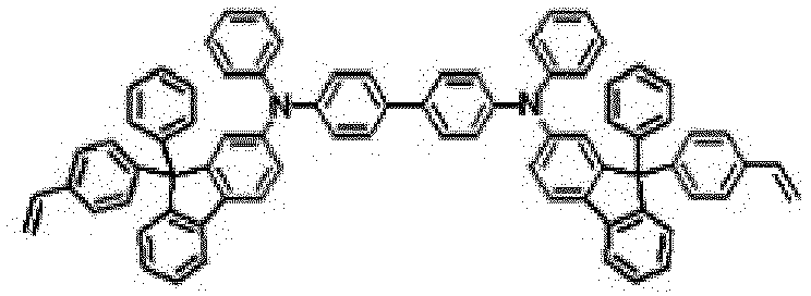

Verbindung 1-5 Verbindung 1-6 

- Tintenzusammensetzung gemäß Anspruch 1, worin das durch die Formel 2 dargestellte Lösungsmittel irgendeines ist, das ausgewählt ist aus den folgenden Verbindung 2-1 bis 2-7:
Verbindung 2-1 Verbindung 2-2 

Verbindung 2-3 Verbindung 2-4 

Verbindung 2-5 Verbindung 2-6 

Verbindung 2-7 
- Tintenzusammensetzung gemäß Anspruch 1, ferner umfassend:
ein Unterlösungsmittel. - Tintenzusammensetzung gemäß Anspruch 7, worin das Unterlösungsmittel 3-Ethylbiphenyl, 2-Isopropylnaphthalin oder 2-Phenylethylalkohol ist.
- Tintenzusammensetzung gemäß Anspruch 1, worin die durch die Formel 1 dargestellte Verbindung in einer Menge von 0,1 Gewichtsteilen bis 10 Gewichtsteilen umfasst ist, bezogen auf 100 Gewichtsteile des gesamten Lösungsmittels.
- Tintenzusammensetzung gemäß Anspruch 1, worin die Tintenzusammensetzung eine Viskosität von 2 cP bis 20 cP aufweist.
- Verfahren zur Herstellung einer organischen lichtemittierenden Vorrichtung, wobei das Verfahren umfasst:Vorbereiten eines Substrats;Bilden einer ersten Elektrode oder eine zweiten Elektrode auf dem Substrat;Bilden einer organischen Materialschicht, die ein oder mehr Schichten aufweist, auf der ersten Elektrode oder der zweiten Elektrode; undBilden einer zweiten Elektrode oder einer ersten Elektrode auf der organischen Materialschicht,worin das Bilden der organischen Materialschicht das Bilden einer organischen Materialschicht, die ein oder mehr Schichten aufweist, unter Verwendung der Tintenzusammensetzung gemäß irgendeinem der Ansprüche 1 bis 10 umfasst.
- Verfahren gemäß Anspruch 11, worin die organische Materialschicht, die unter Verwendung der Tintenzusammensetzung gebildet wird, durch ein Tintenstrahl-Druckverfahren gebildet wird.
- Verfahren gemäß Anspruch 11, worin das organische Materialschicht, die unter Verwendung der Tintenzusammensetzung gebildet wird, eine lichtemittierende Schicht ist.
- Verfahren gemäß Anspruch 11, worin die organische Materialschicht, die unter Verwendung der Tintenzusammensetzung gebildet wird, eine Elektroneninjektionsschicht oder eine Elektronentransportschicht ist.
- Verfahren gemäß Anspruch 11, worin die organische Materialschicht, die unter Verwendung der Tintenzusammensetzung gebildet wird, eine Lochinjektionsschicht, eine Lochtransportschicht oder eine Schicht, die simultan Löcher injiziert oder transportiert, ist.
Applications Claiming Priority (2)
| Application Number | Priority Date | Filing Date | Title |
|---|---|---|---|
| KR20180030985 | 2018-03-16 | ||
| PCT/KR2019/003007 WO2019177410A1 (ko) | 2018-03-16 | 2019-03-15 | 잉크 조성물 및 유기 발광 소자의 제조방법 |
Publications (3)
| Publication Number | Publication Date |
|---|---|
| EP3663368A1 EP3663368A1 (de) | 2020-06-10 |
| EP3663368A4 EP3663368A4 (de) | 2020-11-18 |
| EP3663368B1 true EP3663368B1 (de) | 2021-09-01 |
Family
ID=67908361
Family Applications (1)
| Application Number | Title | Priority Date | Filing Date |
|---|---|---|---|
| EP19767490.6A Active EP3663368B1 (de) | 2018-03-16 | 2019-03-15 | Tintenzusammensetzung und verfahren zur herstellung einer organischen lichtemittierenden vorrichtung |
Country Status (6)
| Country | Link |
|---|---|
| US (1) | US11515476B2 (de) |
| EP (1) | EP3663368B1 (de) |
| JP (1) | JP6910698B2 (de) |
| KR (1) | KR102182179B1 (de) |
| CN (1) | CN111032797B (de) |
| WO (1) | WO2019177410A1 (de) |
Families Citing this family (9)
| Publication number | Priority date | Publication date | Assignee | Title |
|---|---|---|---|---|
| US20230098935A1 (en) * | 2020-01-08 | 2023-03-30 | Lg Chem, Ltd. | Fluorene-Based Compound, Organic Light-Emitting Device Using Same, And Manufacturing Method Therefor |
| KR102820891B1 (ko) * | 2020-07-31 | 2025-06-13 | 주식회사 엘지화학 | 유기 화합물의 제조방법 |
| KR102906834B1 (ko) * | 2020-10-30 | 2025-12-31 | 주식회사 엘지화학 | 중합체 및 이를 이용한 유기 발광 소자 |
| US20240376327A1 (en) * | 2021-09-14 | 2024-11-14 | Lg Chem, Ltd. | Ink Composition, Organic Material Layer Comprising Same, and Organic Light-Emitting Device Comprising Same |
| US20240343930A1 (en) * | 2021-09-14 | 2024-10-17 | Lg Chem, Ltd. | Ink Composition, Organic Material Layer Comprising Same, and Organic Light-Emitting Device Comprising Same |
| CN118251380A (zh) | 2021-11-04 | 2024-06-25 | 多蒂肯独家合成控股公司 | 螺-(茚满-芴)型化合物及其在有机电子器件中的用途 |
| KR102805387B1 (ko) * | 2021-11-29 | 2025-05-13 | 단국대학교 산학협력단 | 유기발광소자의 발광층 잉크 조성물 및 이를 이용하는 유기발광소자의 발광층 제조 방법 |
| WO2024063595A1 (ko) * | 2022-09-23 | 2024-03-28 | 주식회사 엘지화학 | 잉크 조성물, 이를 포함하는 유기물층 및 이를 포함하는 유기 발광 소자 |
| EP4484506A4 (de) * | 2022-09-23 | 2025-08-27 | Lg Chemical Ltd | Tintenzusammensetzung, organische materialschicht damit und organische lichtemittierende vorrichtung damit |
Family Cites Families (25)
| Publication number | Priority date | Publication date | Assignee | Title |
|---|---|---|---|---|
| JP4816687B2 (ja) | 2003-08-14 | 2011-11-16 | 三菱化学株式会社 | 有機電界発光素子用組成物、有機電界発光素子、有機電界発光素子の製造方法及び有機電界発光素子用組成物の保管方法 |
| US7785573B2 (en) | 2006-01-23 | 2010-08-31 | Isp Investments Inc. | Solubilizing agents for active or functional organic compounds |
| JP5298524B2 (ja) * | 2006-12-27 | 2013-09-25 | 三菱化学株式会社 | 架橋基を有する有機化合物、有機電界発光素子材料、有機電界発光素子用組成物および有機電界発光素子 |
| JP5125480B2 (ja) * | 2007-01-15 | 2013-01-23 | 三菱化学株式会社 | 正孔輸送材料、該正孔輸送材料を重合させてなる高分子化合物、有機電界発光素子用組成物および有機電界発光素子 |
| JP5470706B2 (ja) * | 2007-01-25 | 2014-04-16 | 三菱化学株式会社 | 正孔輸送材料、該正孔輸送材料を重合させてなる高分子化合物、有機電界発光素子用組成物および有機電界発光素子 |
| US8586199B2 (en) * | 2007-04-06 | 2013-11-19 | Idemitsu Kosan Co., Ltd. | Organic electroluminescence device |
| JP4990685B2 (ja) * | 2007-06-11 | 2012-08-01 | 凸版印刷株式会社 | 蛍光材料、発光インク組成物および有機el素子 |
| KR20090114716A (ko) * | 2008-04-30 | 2009-11-04 | 덕산하이메탈(주) | 정공수송층 물질 및 이를 포함하는 유기 전계발광 소자 |
| KR101395018B1 (ko) | 2010-05-13 | 2014-05-16 | 주식회사 엘지화학 | 잉크젯용 잉크 조성물, 이를 이용한 컬러필터 및 이를 포함하는 표시장치 |
| EP2428512B1 (de) * | 2010-09-08 | 2014-10-22 | Semiconductor Energy Laboratory Co., Ltd. | Fluorenverbindung, lichtemittierendes Element, lichtemittierende Vorrichtung, elektronische Vorrichtung und Beleuchtungsvorrichtung. |
| EP2610240A1 (de) | 2011-12-28 | 2013-07-03 | Solvay Sa | Vernetzbare Arylamin-Verbindungen |
| CN108863814A (zh) * | 2012-07-23 | 2018-11-23 | 默克专利有限公司 | 芴和含有所述芴的电子器件 |
| KR102109353B1 (ko) | 2013-05-08 | 2020-05-12 | 덕산네오룩스 주식회사 | 유기전기 소자용 화합물, 이를 이용한 유기전기소자 및 그 전자 장치 |
| KR102117603B1 (ko) * | 2014-02-10 | 2020-06-01 | 덕산네오룩스 주식회사 | 유기전기소자용 화합물, 이를 이용한 유기전기소자 및 그 전자 장치 |
| JP6425394B2 (ja) | 2014-03-14 | 2018-11-21 | 出光興産株式会社 | インク組成物、インク組成物を用いた有機エレクトロルミネッセンス素子、及び電子機器 |
| KR102250691B1 (ko) * | 2014-10-06 | 2021-05-13 | 덕산네오룩스 주식회사 | 유기전기 소자용 화합물, 이를 이용한 유기전기소자 및 그 전자 장치 |
| KR102329807B1 (ko) * | 2014-11-05 | 2021-11-22 | 덕산네오룩스 주식회사 | 유기전기소자용 조성물을 이용한 디스플레이 장치 및 유기전기소자 |
| CN107690720B (zh) | 2015-06-12 | 2020-04-03 | 默克专利有限公司 | 作为用于oled制剂的溶剂的含有非芳族环的酯 |
| US20170024344A1 (en) | 2015-07-22 | 2017-01-26 | Microchip Technology Incorporated | Method and System for USB 2.0 Bandwidth Reservation |
| CN111477768B (zh) * | 2015-12-15 | 2023-04-07 | 默克专利有限公司 | 作为用于有机电子制剂的溶剂的含芳族基团的酯 |
| KR102126602B1 (ko) * | 2016-04-22 | 2020-06-24 | 주식회사 엘지화학 | 카바졸 유도체 및 이를 이용한 유기 발광 소자 |
| JP6833388B2 (ja) | 2016-08-01 | 2021-02-24 | 株式会社Joled | 有機el用インク |
| EP3514139B1 (de) | 2017-02-28 | 2024-01-31 | LG Chem, Ltd. | Fluorbasierte verbindung, organische lichtemittierende vorrichtung damit und verfahren zur herstellung davon |
| KR102536248B1 (ko) | 2017-06-21 | 2023-05-25 | 삼성디스플레이 주식회사 | 헤테로시클릭 화합물 및 이를 포함한 유기 발광 소자 |
| KR102217266B1 (ko) | 2018-09-28 | 2021-02-17 | 주식회사 엘지화학 | 유기 발광 소자용 잉크 조성물 |
-
2019
- 2019-03-15 KR KR1020190029611A patent/KR102182179B1/ko active Active
- 2019-03-15 CN CN201980004019.4A patent/CN111032797B/zh active Active
- 2019-03-15 WO PCT/KR2019/003007 patent/WO2019177410A1/ko not_active Ceased
- 2019-03-15 JP JP2020513276A patent/JP6910698B2/ja active Active
- 2019-03-15 EP EP19767490.6A patent/EP3663368B1/de active Active
- 2019-03-15 US US16/641,479 patent/US11515476B2/en active Active
Also Published As
| Publication number | Publication date |
|---|---|
| JP2020532872A (ja) | 2020-11-12 |
| KR20190109295A (ko) | 2019-09-25 |
| CN111032797B (zh) | 2022-03-18 |
| WO2019177410A1 (ko) | 2019-09-19 |
| EP3663368A4 (de) | 2020-11-18 |
| CN111032797A (zh) | 2020-04-17 |
| EP3663368A1 (de) | 2020-06-10 |
| US11515476B2 (en) | 2022-11-29 |
| JP6910698B2 (ja) | 2021-07-28 |
| KR102182179B1 (ko) | 2020-11-24 |
| US20210050523A1 (en) | 2021-02-18 |
Similar Documents
| Publication | Publication Date | Title |
|---|---|---|
| EP3663368B1 (de) | Tintenzusammensetzung und verfahren zur herstellung einer organischen lichtemittierenden vorrichtung | |
| US11472966B2 (en) | Coating composition, organic light-emitting diode using same and method for preparing same | |
| KR102056532B1 (ko) | 플루오렌계 화합물, 이를 이용한 유기 발광 소자 및 이의 제조방법 | |
| EP3683208B1 (de) | Verbindung, beschichtungszusammensetzung damit und vorrichtung mit organischer lichtemittierender diode | |
| KR20190134033A (ko) | 유기 발광 소자 | |
| JP2019533653A (ja) | 化合物、これを含むコーティング組成物、これを用いた有機発光素子およびその製造方法 | |
| EP3680262B1 (de) | Polymer, beschichtungszusammensetzung damit und organische leuchtdiode damit | |
| US11127904B2 (en) | Compound, coating composition comprising same, organic light emitting device using same, and manufacturing method thereof | |
| EP4071193B1 (de) | Neuartiges polymer und organisches lichtemittierendes element damit | |
| KR102489570B1 (ko) | 신규한 고분자 및 이를 이용한 유기 발광 소자 | |
| KR102549459B1 (ko) | 신규한 고분자 및 이를 이용한 유기발광 소자 | |
| JP6683337B2 (ja) | 化合物を含むコーティング組成物およびこれを含む有機発光素子 | |
| KR20210153454A (ko) | 신규한 고분자 및 이를 이용한 유기 발광 소자 | |
| EP4092035B1 (de) | Neuartige verbindung und organische lichtemittierende vorrichtung damit | |
| KR20200029344A (ko) | 신규한 화합물 및 이를 포함하는 유기 발광 소자 | |
| KR20220005338A (ko) | 신규한 고분자 및 이를 이용한 유기 발광 소자 | |
| KR20190134036A (ko) | 유기 발광 소자 | |
| KR102133626B1 (ko) | 코팅 조성물, 이를 이용하여 제조된 유기 발광 소자 및 이의 제조방법 | |
| KR20240176369A (ko) | 신규한 고분자 및 이를 이용한 유기 발광 소자 | |
| KR20220001952A (ko) | 신규한 고분자 및 이를 이용한 유기 발광 소자 |
Legal Events
| Date | Code | Title | Description |
|---|---|---|---|
| STAA | Information on the status of an ep patent application or granted ep patent |
Free format text: STATUS: THE INTERNATIONAL PUBLICATION HAS BEEN MADE |
|
| PUAI | Public reference made under article 153(3) epc to a published international application that has entered the european phase |
Free format text: ORIGINAL CODE: 0009012 |
|
| STAA | Information on the status of an ep patent application or granted ep patent |
Free format text: STATUS: REQUEST FOR EXAMINATION WAS MADE |
|
| 17P | Request for examination filed |
Effective date: 20200306 |
|
| AK | Designated contracting states |
Kind code of ref document: A1 Designated state(s): AL AT BE BG CH CY CZ DE DK EE ES FI FR GB GR HR HU IE IS IT LI LT LU LV MC MK MT NL NO PL PT RO RS SE SI SK SM TR |
|
| AX | Request for extension of the european patent |
Extension state: BA ME |
|
| A4 | Supplementary search report drawn up and despatched |
Effective date: 20201020 |
|
| RIC1 | Information provided on ipc code assigned before grant |
Ipc: C09D 11/38 20140101AFI20201015BHEP Ipc: H01L 51/50 20060101ALI20201015BHEP Ipc: H01L 51/00 20060101ALI20201015BHEP Ipc: C09D 11/36 20140101ALI20201015BHEP |
|
| GRAP | Despatch of communication of intention to grant a patent |
Free format text: ORIGINAL CODE: EPIDOSNIGR1 |
|
| STAA | Information on the status of an ep patent application or granted ep patent |
Free format text: STATUS: GRANT OF PATENT IS INTENDED |
|
| RIN1 | Information on inventor provided before grant (corrected) |
Inventor name: JUNG, JI YOUNG Inventor name: KIM, MI KYOUNG |
|
| INTG | Intention to grant announced |
Effective date: 20210422 |
|
| DAV | Request for validation of the european patent (deleted) | ||
| DAX | Request for extension of the european patent (deleted) | ||
| GRAS | Grant fee paid |
Free format text: ORIGINAL CODE: EPIDOSNIGR3 |
|
| GRAA | (expected) grant |
Free format text: ORIGINAL CODE: 0009210 |
|
| STAA | Information on the status of an ep patent application or granted ep patent |
Free format text: STATUS: THE PATENT HAS BEEN GRANTED |
|
| AK | Designated contracting states |
Kind code of ref document: B1 Designated state(s): AL AT BE BG CH CY CZ DE DK EE ES FI FR GB GR HR HU IE IS IT LI LT LU LV MC MK MT NL NO PL PT RO RS SE SI SK SM TR |
|
| REG | Reference to a national code |
Ref country code: GB Ref legal event code: FG4D |
|
| REG | Reference to a national code |
Ref country code: CH Ref legal event code: EP Ref country code: AT Ref legal event code: REF Ref document number: 1426255 Country of ref document: AT Kind code of ref document: T Effective date: 20210915 |
|
| REG | Reference to a national code |
Ref country code: DE Ref legal event code: R096 Ref document number: 602019007394 Country of ref document: DE |
|
| REG | Reference to a national code |
Ref country code: IE Ref legal event code: FG4D |
|
| REG | Reference to a national code |
Ref country code: LT Ref legal event code: MG9D |
|
| REG | Reference to a national code |
Ref country code: NL Ref legal event code: MP Effective date: 20210901 |
|
| PG25 | Lapsed in a contracting state [announced via postgrant information from national office to epo] |
Ref country code: LT Free format text: LAPSE BECAUSE OF FAILURE TO SUBMIT A TRANSLATION OF THE DESCRIPTION OR TO PAY THE FEE WITHIN THE PRESCRIBED TIME-LIMIT Effective date: 20210901 Ref country code: BG Free format text: LAPSE BECAUSE OF FAILURE TO SUBMIT A TRANSLATION OF THE DESCRIPTION OR TO PAY THE FEE WITHIN THE PRESCRIBED TIME-LIMIT Effective date: 20211201 Ref country code: HR Free format text: LAPSE BECAUSE OF FAILURE TO SUBMIT A TRANSLATION OF THE DESCRIPTION OR TO PAY THE FEE WITHIN THE PRESCRIBED TIME-LIMIT Effective date: 20210901 Ref country code: FI Free format text: LAPSE BECAUSE OF FAILURE TO SUBMIT A TRANSLATION OF THE DESCRIPTION OR TO PAY THE FEE WITHIN THE PRESCRIBED TIME-LIMIT Effective date: 20210901 Ref country code: NO Free format text: LAPSE BECAUSE OF FAILURE TO SUBMIT A TRANSLATION OF THE DESCRIPTION OR TO PAY THE FEE WITHIN THE PRESCRIBED TIME-LIMIT Effective date: 20211201 Ref country code: SE Free format text: LAPSE BECAUSE OF FAILURE TO SUBMIT A TRANSLATION OF THE DESCRIPTION OR TO PAY THE FEE WITHIN THE PRESCRIBED TIME-LIMIT Effective date: 20210901 Ref country code: RS Free format text: LAPSE BECAUSE OF FAILURE TO SUBMIT A TRANSLATION OF THE DESCRIPTION OR TO PAY THE FEE WITHIN THE PRESCRIBED TIME-LIMIT Effective date: 20210901 Ref country code: ES Free format text: LAPSE BECAUSE OF FAILURE TO SUBMIT A TRANSLATION OF THE DESCRIPTION OR TO PAY THE FEE WITHIN THE PRESCRIBED TIME-LIMIT Effective date: 20210901 |
|
| REG | Reference to a national code |
Ref country code: AT Ref legal event code: MK05 Ref document number: 1426255 Country of ref document: AT Kind code of ref document: T Effective date: 20210901 |
|
| PG25 | Lapsed in a contracting state [announced via postgrant information from national office to epo] |
Ref country code: PL Free format text: LAPSE BECAUSE OF FAILURE TO SUBMIT A TRANSLATION OF THE DESCRIPTION OR TO PAY THE FEE WITHIN THE PRESCRIBED TIME-LIMIT Effective date: 20210901 Ref country code: LV Free format text: LAPSE BECAUSE OF FAILURE TO SUBMIT A TRANSLATION OF THE DESCRIPTION OR TO PAY THE FEE WITHIN THE PRESCRIBED TIME-LIMIT Effective date: 20210901 Ref country code: GR Free format text: LAPSE BECAUSE OF FAILURE TO SUBMIT A TRANSLATION OF THE DESCRIPTION OR TO PAY THE FEE WITHIN THE PRESCRIBED TIME-LIMIT Effective date: 20211202 |
|
| PG25 | Lapsed in a contracting state [announced via postgrant information from national office to epo] |
Ref country code: AT Free format text: LAPSE BECAUSE OF FAILURE TO SUBMIT A TRANSLATION OF THE DESCRIPTION OR TO PAY THE FEE WITHIN THE PRESCRIBED TIME-LIMIT Effective date: 20210901 |
|
| PG25 | Lapsed in a contracting state [announced via postgrant information from national office to epo] |
Ref country code: IS Free format text: LAPSE BECAUSE OF FAILURE TO SUBMIT A TRANSLATION OF THE DESCRIPTION OR TO PAY THE FEE WITHIN THE PRESCRIBED TIME-LIMIT Effective date: 20220101 Ref country code: SM Free format text: LAPSE BECAUSE OF FAILURE TO SUBMIT A TRANSLATION OF THE DESCRIPTION OR TO PAY THE FEE WITHIN THE PRESCRIBED TIME-LIMIT Effective date: 20210901 Ref country code: SK Free format text: LAPSE BECAUSE OF FAILURE TO SUBMIT A TRANSLATION OF THE DESCRIPTION OR TO PAY THE FEE WITHIN THE PRESCRIBED TIME-LIMIT Effective date: 20210901 Ref country code: RO Free format text: LAPSE BECAUSE OF FAILURE TO SUBMIT A TRANSLATION OF THE DESCRIPTION OR TO PAY THE FEE WITHIN THE PRESCRIBED TIME-LIMIT Effective date: 20210901 Ref country code: PT Free format text: LAPSE BECAUSE OF FAILURE TO SUBMIT A TRANSLATION OF THE DESCRIPTION OR TO PAY THE FEE WITHIN THE PRESCRIBED TIME-LIMIT Effective date: 20220103 Ref country code: NL Free format text: LAPSE BECAUSE OF FAILURE TO SUBMIT A TRANSLATION OF THE DESCRIPTION OR TO PAY THE FEE WITHIN THE PRESCRIBED TIME-LIMIT Effective date: 20210901 Ref country code: EE Free format text: LAPSE BECAUSE OF FAILURE TO SUBMIT A TRANSLATION OF THE DESCRIPTION OR TO PAY THE FEE WITHIN THE PRESCRIBED TIME-LIMIT Effective date: 20210901 Ref country code: CZ Free format text: LAPSE BECAUSE OF FAILURE TO SUBMIT A TRANSLATION OF THE DESCRIPTION OR TO PAY THE FEE WITHIN THE PRESCRIBED TIME-LIMIT Effective date: 20210901 Ref country code: AL Free format text: LAPSE BECAUSE OF FAILURE TO SUBMIT A TRANSLATION OF THE DESCRIPTION OR TO PAY THE FEE WITHIN THE PRESCRIBED TIME-LIMIT Effective date: 20210901 |
|
| REG | Reference to a national code |
Ref country code: DE Ref legal event code: R097 Ref document number: 602019007394 Country of ref document: DE |
|
| PLBE | No opposition filed within time limit |
Free format text: ORIGINAL CODE: 0009261 |
|
| STAA | Information on the status of an ep patent application or granted ep patent |
Free format text: STATUS: NO OPPOSITION FILED WITHIN TIME LIMIT |
|
| PG25 | Lapsed in a contracting state [announced via postgrant information from national office to epo] |
Ref country code: IT Free format text: LAPSE BECAUSE OF FAILURE TO SUBMIT A TRANSLATION OF THE DESCRIPTION OR TO PAY THE FEE WITHIN THE PRESCRIBED TIME-LIMIT Effective date: 20210901 Ref country code: DK Free format text: LAPSE BECAUSE OF FAILURE TO SUBMIT A TRANSLATION OF THE DESCRIPTION OR TO PAY THE FEE WITHIN THE PRESCRIBED TIME-LIMIT Effective date: 20210901 |
|
| 26N | No opposition filed |
Effective date: 20220602 |
|
| PG25 | Lapsed in a contracting state [announced via postgrant information from national office to epo] |
Ref country code: SI Free format text: LAPSE BECAUSE OF FAILURE TO SUBMIT A TRANSLATION OF THE DESCRIPTION OR TO PAY THE FEE WITHIN THE PRESCRIBED TIME-LIMIT Effective date: 20210901 |
|
| PG25 | Lapsed in a contracting state [announced via postgrant information from national office to epo] |
Ref country code: MC Free format text: LAPSE BECAUSE OF FAILURE TO SUBMIT A TRANSLATION OF THE DESCRIPTION OR TO PAY THE FEE WITHIN THE PRESCRIBED TIME-LIMIT Effective date: 20210901 |
|
| REG | Reference to a national code |
Ref country code: CH Ref legal event code: PL |
|
| REG | Reference to a national code |
Ref country code: BE Ref legal event code: MM Effective date: 20220331 |
|
| PG25 | Lapsed in a contracting state [announced via postgrant information from national office to epo] |
Ref country code: IE Free format text: LAPSE BECAUSE OF NON-PAYMENT OF DUE FEES Effective date: 20220315 Ref country code: CH Free format text: LAPSE BECAUSE OF NON-PAYMENT OF DUE FEES Effective date: 20220331 Ref country code: LU Free format text: LAPSE BECAUSE OF NON-PAYMENT OF DUE FEES Effective date: 20220315 Ref country code: LI Free format text: LAPSE BECAUSE OF NON-PAYMENT OF DUE FEES Effective date: 20220331 |
|
| PG25 | Lapsed in a contracting state [announced via postgrant information from national office to epo] |
Ref country code: BE Free format text: LAPSE BECAUSE OF NON-PAYMENT OF DUE FEES Effective date: 20220331 |
|
| PG25 | Lapsed in a contracting state [announced via postgrant information from national office to epo] |
Ref country code: MK Free format text: LAPSE BECAUSE OF FAILURE TO SUBMIT A TRANSLATION OF THE DESCRIPTION OR TO PAY THE FEE WITHIN THE PRESCRIBED TIME-LIMIT Effective date: 20210901 Ref country code: CY Free format text: LAPSE BECAUSE OF FAILURE TO SUBMIT A TRANSLATION OF THE DESCRIPTION OR TO PAY THE FEE WITHIN THE PRESCRIBED TIME-LIMIT Effective date: 20210901 |
|
| PG25 | Lapsed in a contracting state [announced via postgrant information from national office to epo] |
Ref country code: HU Free format text: LAPSE BECAUSE OF FAILURE TO SUBMIT A TRANSLATION OF THE DESCRIPTION OR TO PAY THE FEE WITHIN THE PRESCRIBED TIME-LIMIT; INVALID AB INITIO Effective date: 20190315 |
|
| PG25 | Lapsed in a contracting state [announced via postgrant information from national office to epo] |
Ref country code: MT Free format text: LAPSE BECAUSE OF FAILURE TO SUBMIT A TRANSLATION OF THE DESCRIPTION OR TO PAY THE FEE WITHIN THE PRESCRIBED TIME-LIMIT Effective date: 20210901 |
|
| PGFP | Annual fee paid to national office [announced via postgrant information from national office to epo] |
Ref country code: DE Payment date: 20250220 Year of fee payment: 7 |
|
| PGFP | Annual fee paid to national office [announced via postgrant information from national office to epo] |
Ref country code: FR Payment date: 20250221 Year of fee payment: 7 |
|
| PGFP | Annual fee paid to national office [announced via postgrant information from national office to epo] |
Ref country code: GB Payment date: 20250224 Year of fee payment: 7 |
|
| PG25 | Lapsed in a contracting state [announced via postgrant information from national office to epo] |
Ref country code: TR Free format text: LAPSE BECAUSE OF FAILURE TO SUBMIT A TRANSLATION OF THE DESCRIPTION OR TO PAY THE FEE WITHIN THE PRESCRIBED TIME-LIMIT Effective date: 20210901 |