EP3661042A1 - Dispositif de conversion de puissance électrique - Google Patents
Dispositif de conversion de puissance électrique Download PDFInfo
- Publication number
- EP3661042A1 EP3661042A1 EP18837405.2A EP18837405A EP3661042A1 EP 3661042 A1 EP3661042 A1 EP 3661042A1 EP 18837405 A EP18837405 A EP 18837405A EP 3661042 A1 EP3661042 A1 EP 3661042A1
- Authority
- EP
- European Patent Office
- Prior art keywords
- electric
- conversion device
- semiconductor module
- power conversion
- power semiconductor
- Prior art date
- Legal status (The legal status is an assumption and is not a legal conclusion. Google has not performed a legal analysis and makes no representation as to the accuracy of the status listed.)
- Withdrawn
Links
Images


Classifications
-
- H—ELECTRICITY
- H02—GENERATION; CONVERSION OR DISTRIBUTION OF ELECTRIC POWER
- H02M—APPARATUS FOR CONVERSION BETWEEN AC AND AC, BETWEEN AC AND DC, OR BETWEEN DC AND DC, AND FOR USE WITH MAINS OR SIMILAR POWER SUPPLY SYSTEMS; CONVERSION OF DC OR AC INPUT POWER INTO SURGE OUTPUT POWER; CONTROL OR REGULATION THEREOF
- H02M7/00—Conversion of ac power input into dc power output; Conversion of dc power input into ac power output
- H02M7/003—Constructional details, e.g. physical layout, assembly, wiring or busbar connections
-
- H—ELECTRICITY
- H05—ELECTRIC TECHNIQUES NOT OTHERWISE PROVIDED FOR
- H05K—PRINTED CIRCUITS; CASINGS OR CONSTRUCTIONAL DETAILS OF ELECTRIC APPARATUS; MANUFACTURE OF ASSEMBLAGES OF ELECTRICAL COMPONENTS
- H05K7/00—Constructional details common to different types of electric apparatus
- H05K7/14—Mounting supporting structure in casing or on frame or rack
- H05K7/1422—Printed circuit boards receptacles, e.g. stacked structures, electronic circuit modules or box like frames
- H05K7/1427—Housings
- H05K7/1432—Housings specially adapted for power drive units or power converters
- H05K7/14329—Housings specially adapted for power drive units or power converters specially adapted for the configuration of power bus bars
-
- H—ELECTRICITY
- H05—ELECTRIC TECHNIQUES NOT OTHERWISE PROVIDED FOR
- H05K—PRINTED CIRCUITS; CASINGS OR CONSTRUCTIONAL DETAILS OF ELECTRIC APPARATUS; MANUFACTURE OF ASSEMBLAGES OF ELECTRICAL COMPONENTS
- H05K7/00—Constructional details common to different types of electric apparatus
- H05K7/20—Modifications to facilitate cooling, ventilating, or heating
- H05K7/2089—Modifications to facilitate cooling, ventilating, or heating for power electronics, e.g. for inverters for controlling motor
- H05K7/20909—Forced ventilation, e.g. on heat dissipaters coupled to components
- H05K7/20918—Forced ventilation, e.g. on heat dissipaters coupled to components the components being isolated from air flow, e.g. hollow heat sinks, wind tunnels or funnels
Definitions
- the present invention relates to a mounting structure of equipment in an electric-power conversion device, and is particularly suitable by being applied to an electric-power conversion device in which a power semiconductor module is mounted.
- An electric-power conversion device installed in a railroad vehicle is a device that controls an electric motor that drives a vehicle such as an electric railroad vehicle.
- the electric-power conversion device is mainly installed under the floor of a vehicle, and converts electric power input from a railroad wire by switching operations of a main circuit including plural power semiconductor modules.
- the converted electric power is used to control an electric motor for railroad vehicles.
- the main circuit that is a primary constitutional device of the electric-power conversion device includes, for example, a power semiconductor module having a power switching element, a gate drive device that is a driving circuit thereof, and a filter capacitor that stabilizes DC electric power input from a wire (see Patent Literature 1).
- Patent Literature 1 Japanese Unexamined Patent Application Publication No. Hei11 (1999)-251499
- the height dimension of the electric-power conversion device in the vertical direction has been one of restrictions when being installed in a relation of a distance to the ground surface.
- the present invention has been made in consideration of the above-described point, and proposes an electric-power conversion device that can be easily mounted in a low floor vehicle while suppressing the height dimension in the vertical direction when being installed.
- the present invention provides an electric-power conversion device comprising: a power semiconductor module in which each of an upper arm power switching element and a lower arm power switching element is driven in accordance with conduction modes to a P-pole terminal and an N-pole terminal; a gate drive device that controls conduction to the power semiconductor module through the P-pole terminal and the N-pole terminal; a filter capacitor in which plural terminals each of which is connected to the P-pole terminal and the N-pole terminal are formed on the power semiconductor module side; a cooler that cools the power semiconductor module through a predetermined surface with which the power semiconductor module comes into contact; and plural thin plate-shaped busbars that electrically connect the P-pole terminal and the N-pole terminal to the plural terminals, wherein the filter capacitor is arranged near the power semiconductor module along the predetermined surface and the plural terminals are arranged on the side of the P-pole terminal and the N-pole terminal, and wherein the plural thin plate-shaped busbars are formed substantially in parallel with the vertical direction with respect to the
- an electric-power conversion device can be easily mounted in a low floor vehicle while suppressing the height dimension in the vertical direction when being installed.
- Fig. 1 shows an outlined configuration example of a railroad vehicle including an electric-power conversion device 1 according to a first embodiment.
- the railroad vehicle is a low floor vehicle that runs with wheels 109 on railroad tracks 110 by using power (not shown), and includes an air blower 105, a ventilation chamber 102, and the electric-power conversion device 1 under the floor of a vehicle body 104.
- the electric-power conversion device 1 is housed in a housing 101 attached to the floor of the vehicle body 104, and is cooled by exposing a heat radiation member to cooling air 103 flowing in the ventilation chamber 102 in the case of, for example, an air-cooling type.
- a configuration of the electric-power conversion device 1 will be described in detail.
- FIG. 2 shows an example of an appearance in the case of viewing an upper surface of the electric-power conversion device 1 from the upper side
- Fig. 3 shows an example of an appearance in the case of viewing a bottom surface of the electric-power conversion device 1 from the lower side
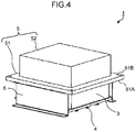
- Fig. 4 shows an example of an appearance in the case of viewing a side surface of the electric-power conversion device 1 from a point positioned slightly upward.
- the electric-power conversion device 1 is a device that generates a DC from a single-phase AC, or generates a three-phase AC from a DC.
- the former is referred to as a converter whereas the latter is referred to as an inverter.
- the converter converts a single-phase AC voltage from an AC power supply into a DC voltage, has a function of charging a filter capacitor 3 for smoothing a DC voltage, and is configured using a two-phase leg.
- the inverter has a function of converting a DC voltage charged to the filter capacitor 3 into an AC voltage by continuously changing a ratio of ON/OFF of each power switching element included in a power semiconductor module, and configures a three-phase leg. Accordingly, the inverter generates a three-phase AC, energizes each power switching element of the power semiconductor module using the three-phase AC through a U-phase busbar 91, a V-phase busbar 92, and a W-phase busbar 93, and drives an electric motor (not shown) mounted in a wagon installed under the floor of the vehicle body 104. Both of the converter and the inverter convert electric power by controlling the conduction of each power switching element.
- a power switching element there is an Si-IGBT characterized in that ON resistance and a driving current are small and a switching speed is fast.
- an SiC-MOSFET that can perform a faster switching operation may be employed.
- the electric-power conversion device 1 basically includes a support frame (frame) 6, a power semiconductor module, a cooler 5, busbars 7, 8, and 9, the filter capacitor 3, and a gate drive device 4.
- the power semiconductor module 2 includes, for example, U-phase, V-phase, and W-phase power switching elements having the P-pole and N-pole. Each power switching element generates heat when being in a conductive state and being cutoff.
- the power semiconductor module 2 will be described later in detail.
- the cooler 5 has a function of cooling the power semiconductor module that largely consumes electric power to generate heat when being in a conductive state and being cutoff.
- An air-cooling type or a water-cooling type can be employed for the cooler 5.
- As the air-cooling type a radiator type, a heat pipe type, or a fin type can be employed.
- the cooler 5 includes, for example, a rectangular flat plate-like cooling block 51, and includes a box-like heat radiation member 52 arranged nearly in the center of one surface (corresponding to a surface facing upward in the drawing) of the cooling block 51.
- the cooler 5 is supported by support frames 6 around rectangular both side parts facing each other in the other surface 51A (corresponding to a surface facing downward in the drawing) of the cooling block 51.
- the power semiconductor module 2 is arranged along the other surface 51A.
- the other surface 51A is also referred to as an "element attachment surface".
- the support frames 6 are basic structures configuring the electric-power conversion device 1, and are used, as the function thereof, when being fixed to the housing 101 or when holding the cooler 5 or other constitutional devices.
- These support frames 6 are rectangular flat plate-like members fixed so as to rise nearly in the vertical direction from the other surface 51A of the cooling block 51, and other side members of the flat plate parts that do not come into contact with the other surface 51A of the cooling block 51 are configured to be bent outward in the direction parallel to the other surface 51A. Surfaces on one side of the other side members configured to be bent are fixed to, for example, a bottom part of the low floor vehicle when the electric-power conversion device 1 is attached to the bottom part.
- Fig. 5 shows a configuration example of a main circuit and a control logic unit 100 of the electric-power conversion device 1.
- feeding systems of a railroad there are an AC-type system and a DC-type system in general.
- main electric motors there are an AC electric motor and a DC electric motor.
- an inverter or a converter, or a combination thereof can be used in the electric-power conversion device 1 in accordance with a combination of a feeding system and an electric motor.
- an inverter applied to a combination of a DC feeding system and an AC electric motor will be described as an example.
- the main circuit in the embodiment is configured to have the filter capacitor 3 and a three-phase inverter connected in electric circuit paths between the P-pole busbar 7 and the N-pole busbar 8 that are DC terminals.
- the three-phase inverter converts an input DC into a three-phase AC having an arbitrary frequency and an arbitrary voltage, and outputs the three-phase AC to AC terminals U, V, and W.
- the three-phase inverter includes six groups of power switching elements (PU, NU, PV, NV, PW, and NW) of a U-phase 211, a V-phase 212, and a W-phase 213.
- the power switching element in each phase includes an element and a freewheel diode connected in parallel with the element.
- Si-IGBT is an example of a circuit symbol as the power switching element, but SiC-MOSFET may be used instead.
- the control logic unit 100 is provided separately from the electric-power conversion device 1, and outputs a control signal to the electric-power conversion device 1 through the gate drive device 4 in conduction control.
- the control logic unit 100 drives each power switching element of the power semiconductor module 2 using the control signal.
- the gate drive device 4 is arranged on the surface side opposite to the cooler 5 with the filter capacitor 3 therebetween. Electronic components mounted in the gate drive device 4 may malfunction due to heat or the lifetime of the gate drive device 4 may become short. For example, the power semiconductor module 2 and wirings such as the busbars 7, 8, and 9 generate heat by themselves, and the temperature of the vicinity thereof possibly increases. Thus, the gate drive device 4 is desirably arranged at a position where a thermal influence by the surrounding heating components can be avoided.
- Fig. 6 is a cross-sectional view for showing an example of a basic configuration of the electric-power conversion device 1
- Fig. 7 is a diagram obtained by enlarging a part denoted by a range W shown in Fig. 6
- Fig. 8 is a perspective view for showing a configuration example when the main circuit part of the electric-power conversion device 1 shown in Fig. 2 is viewed from the element attachment surface side.
- Fig. 9(A) and Fig. 9(B) are a plan view and a circuit diagram for showing a configuration example of the power semiconductor module 2, respectively.
- Fig. 10 is a perspective view of the power semiconductor module 2 shown in Fig. 9(A) .
- a configuration example of the power semiconductor module 2 will be described using Fig. 9(A), Fig. 9(B), and Fig. 10 .
- the 2iN1 means that an element group 11 of a P-pole upper arm and an element group 12 of an N-pole lower arm shown in Fig. 9(B) are stored in one package.
- P-pole terminals 21 and N-pole terminals 22 can be closely arranged as shown in Fig. 9(A) and Fig. 10 .
- the P-pole terminals 21, the N-pole terminals 22, M-pole terminals 23, and signal input terminals 24 and 25 are provided in the package.
- the signal input terminals 24 are terminals for driving the element group 11 of the upper arm and the signal input terminals 25 are terminals for driving the element group 12 of the lower arm.
- the power semiconductor module 2 is attached to the cooler 5 including the cooling block 51 and the heat radiation member 52 so that the side of the P-pole terminals 21 and the N-pole terminals 22 faces inward and the side of the M-pole terminals 23 faces outward.
- the busbars 7, 8, 9, 13, and 14 are provided in the electric-power conversion device 1 to be electrically connected to external devices. It should be noted that the P-pole busbar 7 and the N-pole busbar 8 show end portions of the busbars 13 and 14, respectively.
- copper having a small volume resistivity is employed and the cross-sectional area of a conductor is configured to be large in order to suppress heating of the conductor. Especially in the case where light weight is required, aluminum is employed in some cases as the material.
- Electric connection between the P-pole terminals 21 and the N-pole terminals 22 of the power semiconductor module 2 and each terminal 10 of the filter capacitor 3 is secured by closely arranging the thin plate-like busbars 13 and 14 to which films are attached for insulation.
- the inductance of the main circuit can be reduced by the existence of the busbars 13 and 14.
- the P-pole thin-plate-shaped busbar 13 and the N-pole thin-plate-shaped busbar 14 for electrically connecting the power semiconductor module 2 and the filter capacitor 3 to each other stand in the direction vertical to the attachment surface of the power semiconductor module 2, and are fixed to the P-pole terminals 21 and the N-pole terminals 22 while being close to each other in the facing direction.
- This configuration is employed to reduce the inductance of the P-pole thin-plate-shaped busbar 13 and the N-pole thin-plate-shaped busbar 14. As a distance between the P-pole thin-plate-shaped busbar 13 and the N-pole thin-plate-shaped busbar 14 becomes shorter, the inductance can be reduced. However, such a configuration causes low withstand voltage, resulting in a restriction.
- the filter capacitor 3 is provided near the power semiconductor module 2 along the longitudinal direction of the power semiconductor module 2 and an element attachment surface 51A of the cooling block 51 of the cooler 5, and plural terminals 10 are arranged on the side of the P-pole terminals 21 and the N-pole terminals 22. Namely, the plural terminals 10 of the filter capacitor 3 are provided on the side of the power semiconductor module 2 in the horizontal direction in the direction of the line drawings shown in Fig. 6 and Fig. 7 , and connects the P-pole thin-plate-shaped busbar 13 and the N-pole thin-plate-shaped busbar 14 to each other.
- the gate drive device 4 In general, there is a possibility that electronic components mounted in the gate drive device 4 shown in Fig. 6 malfunction due to heat or the lifetime of the gate drive device 4 becomes short.
- the power semiconductor module 2, wirings, the busbars, and the like generate heat by themselves, and the temperature of the vicinity thereof possibly increases.
- the gate drive device 4 is required to be arranged while avoiding a thermal influence by the surrounding heating components, and thus is arranged just below the filter capacitor 3 in the direction of the line drawings shown in Fig. 6 and Fig. 7 .
- the filter capacitor 3 does not overlap with the gate drive device 4 on the terminal surface side (just below the power semiconductor module 2 in the direction of the line drawings shown in Fig. 6 and Fig. 7 ) of the power semiconductor module 2, and thus the height of the power semiconductor module 2, a spatial insulation distance to the gate drive device 4, and the like can be ignored.
- the height dimension A of the electric-power conversion device 1 according to the embodiment is minimized in the vertical direction as shown in Fig. 6 , and mounting of the electric-power conversion device 1 into the low floor vehicle becomes easier.
- a distance B between the P-pole terminals 21 and the N-pole terminals 22 of the power semiconductor module 2 and the terminals 10 of the filter capacitor 3 can be minimized, and thus the inductance of the main circuit can be reduced.
- V L ⁇ di / dt
- the inductance L can be suppressed to a minimum, and thus the restriction as described above can be minimized.
- An electric-power conversion device 1A according to a second embodiment has substantially the same configuration and executes substantially the same operation as the electric-power conversion device 1 according to the first embodiment, and thus the explanation of the same configuration and operation will be omitted, and different points will be mainly described below.
- Fig. 11 is a perspective view for showing a configuration example of the electric-power conversion device 1A according to the second embodiment.
- a fin type is employed for the heat radiation member 52 of the cooler 5.
- the attachment direction of the power semiconductor module 2 matches that of a planar heat radiation fin 15. Namely, the heat radiation fin 15 is attached along the arrangement direction of the P-pole terminals 21 and the N-pole terminals 22 in the power semiconductor module 2.
- the configurations of the P-pole thin-plate-shaped busbar 13 and the N-pole thin-plate-shaped busbar 14 can be simplified, and the width dimension W of the cooling block 51 can be suppressed to be small.
- the cross-sectional area of the passage of the ventilation chamber 102 (see Fig. 1 ) can be reduced. Accordingly, the size of the electric-power conversion device 1A can be made smaller.
- An electric-power conversion device 1B according to a third embodiment has substantially the same configuration and executes substantially the same operation as the electric-power conversion device 1 according to the first embodiment, and thus the explanation of the same configuration and operation will be omitted, and different points will be mainly described below.
- Fig. 12 is a perspective view for showing a configuration example of the electric-power conversion device 1B according to the third embodiment.
- a heat pipe type is employed for the heat radiation member 52 of the cooler 5.
- An electric-power conversion device 1C according to a fourth embodiment has substantially the same configuration and executes substantially the same operation as the electric-power conversion device 1 according to the first embodiment, and thus the explanation of the same configuration and operation will be omitted, and different points will be mainly described below.
- Fig. 13 is a perspective view for showing a configuration example of the electric-power conversion device 1C according to the fourth embodiment.
- a radiator type is employed for the heat radiation member 52 of the cooler 5.
- An electric-power conversion device 1D according to a fifth embodiment has substantially the same configuration and executes substantially the same operation as the electric-power conversion device 1 according to the first embodiment, and thus the explanation of the same configuration and operation will be omitted, and different points will be mainly described below.
- Fig. 14 is a perspective view for showing a configuration example of the electric-power conversion device 1D according to the fifth embodiment.
- a water cooling-type cooler 5 is employed instead of the cooler 5 in the above-described embodiments.
- the water cooling-type does not need to include the heat radiation member 52 exposed to the cooling air 103 in the cooler 5.
- the electric-power conversion device 1D can be further made thinner as compared to the electric-power conversion device 1 according to the first embodiment.
- An electric-power conversion device 1E according to a sixth embodiment has substantially the same configuration and executes substantially the same operation as the electric-power conversion device 1 according to the first embodiment, and thus the explanation of the same configuration and operation will be omitted, and different points will be mainly described below.
- Fig. 15 is a plan view for showing a configuration example of the electric-power conversion device 1E according to the sixth embodiment.
- the filter capacitor 3 is arranged on the windward side of the power semiconductor module 2.
- the filter capacitor 3 can be used even at a higher temperature of surrounding environments by arranging the filter capacitor 3 on the windward side of cooling air CA of the power semiconductor module 2 that generates heat as shown by a sign SH.
- An electric-power conversion device 1F according to a seventh embodiment has substantially the same configuration and executes substantially the same operation as the electric-power conversion device 1 according to the first embodiment, and thus the explanation of the same configuration and operation will be omitted, and different points will be mainly described below.
- Fig. 16 is a plan view for showing a partial configuration example of the electric-power conversion device 1F according to the seventh embodiment.
- the terminal 10 of the filter capacitor 3 is arranged at a position eccentric relative to the center of the filter capacitor 3 in the vertical direction of the element attachment surface 51A. Namely, a dimension C from the element attachment surface 51A of the cooling block 51 in the filter capacitor 3 in the vertical direction to the center of the terminal 10 is not equal to a dimension D from a surface opposite to the surface in contact with the element attachment surface 51A to the center.
- the inductance L of the main circuit can be reduced by minimizing a distance B between the P-pole terminals 21 or the N-pole terminals 22 of the power semiconductor module 2 and the terminal 10 of the filter capacitor 3 while securing a spatial insulation distance and a creepage distance.
- An electric-power conversion device 1G according to an eighth embodiment has substantially the same configuration and executes substantially the same operation as the electric-power conversion device 1 according to the first embodiment, and thus the explanation of the same configuration and operation will be omitted, and different points will be mainly described below.
- Fig. 17 is a plan view for showing a configuration example of the electric-power conversion device 1G according to the eighth embodiment.
- a gap S is provided between a surface of the cooling block 51 facing the filter capacitor 3 and a surface of the filter capacitor 3 facing the cooling block 51. It should be noted that the gap S is provided on an entire surface or a partial surface where the filter capacitor 3 and the cooling block 51 face each other.
- the filter capacitor 3 is hardly affected by heat from the power semiconductor module 2 by providing the air layer between the filter capacitor 3 and the cooling block 51 for heat insulation.
- the allowable temperature of the filter capacitor 3 is lower than that of the power semiconductor module 2, even in the case where the electric-power conversion device is used in a state where the temperature of the cooling block 51 exceeds that of the filter capacitor 3, the cooling efficiency is improved because the cooling air passes through the gap S.
- the cooling air may pass through the gap S by providing a fan at the support frame 6 or in the housing 101 to circulate the cooling air in the housing 101.
- An electric-power conversion device 1H according to a ninth embodiment has substantially the same configuration and executes substantially the same operation as the electric-power conversion device 1G according to the eighth embodiment, and thus the explanation of the same configuration and operation will be omitted, and different points will be mainly described below.
- Fig. 18 is a plan view for showing a configuration example of the electric-power conversion device 1H according to the ninth embodiment.
- the gap S is provided between a surface of the cooling block 51 facing the filter capacitor 3 and a surface of the filter capacitor 3 facing the cooling block 51, and further the gap S is filled with a heat insulating member 17.
- the heat insulating member 17 filled in the gap S is provided on an entire surface or a partial surface where the filter capacitor 3 and the cooling block 51 face each other.
- the cooling efficiency is further improved depending on the material of the heat insulating member 17 as compared to the eighth embodiment.
- An electric-power conversion device 1I according to a tenth embodiment has substantially the same configuration and executes substantially the same operation as the electric-power conversion device 1 according to the first embodiment, and thus the explanation of the same configuration and operation will be omitted, and different points will be mainly described below.
- Fig. 19 is a plan view for showing a configuration example of the electric-power conversion device 1I according to the tenth embodiment.
- the heat radiation member 52 of the cooler 5 for cooling heat SH generated by the power semiconductor module 2 is provided substantially right above the element attachment surface that is a contact surface between the power semiconductor module 2 and the cooling block 51.
- the weight of the electric-power conversion device 1I can be reduced.
- the weight balance of the whole electric-power conversion device 1 can be improved by shifting the position of the center of gravity to the center of the electric-power conversion device 1I as near as possible.
- the power of the above-described air blower 105 (see Fig. 1 ) can be suppressed to a minimum by minimizing the length in the ventilation direction with respect to the cooling air.
- the light weight of the air blower 105 and energy saving by power saving can be realized, and the running cost can be reduced.
- the present invention can be widely applied to an electric-power conversion device in which a power semiconductor module is mounted.
Landscapes
- Engineering & Computer Science (AREA)
- Microelectronics & Electronic Packaging (AREA)
- Physics & Mathematics (AREA)
- Thermal Sciences (AREA)
- Power Engineering (AREA)
- Inverter Devices (AREA)
Applications Claiming Priority (2)
| Application Number | Priority Date | Filing Date | Title |
|---|---|---|---|
| JP2017147141 | 2017-07-28 | ||
| PCT/JP2018/012829 WO2019021532A1 (fr) | 2017-07-28 | 2018-03-28 | Dispositif de conversion de puissance électrique |
Publications (2)
| Publication Number | Publication Date |
|---|---|
| EP3661042A1 true EP3661042A1 (fr) | 2020-06-03 |
| EP3661042A4 EP3661042A4 (fr) | 2021-03-31 |
Family
ID=65039506
Family Applications (1)
| Application Number | Title | Priority Date | Filing Date |
|---|---|---|---|
| EP18837405.2A Withdrawn EP3661042A4 (fr) | 2017-07-28 | 2018-03-28 | Dispositif de conversion de puissance électrique |
Country Status (4)
| Country | Link |
|---|---|
| EP (1) | EP3661042A4 (fr) |
| JP (1) | JP6837554B2 (fr) |
| CN (1) | CN110710094B (fr) |
| WO (1) | WO2019021532A1 (fr) |
Families Citing this family (4)
| Publication number | Priority date | Publication date | Assignee | Title |
|---|---|---|---|---|
| JP6867432B2 (ja) | 2019-05-09 | 2021-04-28 | 三菱電機株式会社 | 電力変換装置 |
| JP7408941B2 (ja) * | 2019-07-25 | 2024-01-09 | 富士電機株式会社 | 電力変換装置 |
| WO2023079685A1 (fr) * | 2021-11-05 | 2023-05-11 | 東芝三菱電機産業システム株式会社 | Sous-module de dispositif de conversion de puissance |
| JPWO2023188043A1 (fr) * | 2022-03-29 | 2023-10-05 |
Family Cites Families (15)
| Publication number | Priority date | Publication date | Assignee | Title |
|---|---|---|---|---|
| JP3229931B2 (ja) * | 1997-09-08 | 2001-11-19 | 三菱電機株式会社 | 3レベル電力変換装置 |
| JP3367411B2 (ja) | 1998-03-06 | 2003-01-14 | 株式会社日立製作所 | 電力変換装置 |
| JP3950836B2 (ja) * | 2003-10-16 | 2007-08-01 | 株式会社東芝 | 車両用制御装置 |
| US7869208B2 (en) * | 2008-12-31 | 2011-01-11 | Caterpillar Inc | Electronics component packaging for power converter |
| CN102474193B (zh) * | 2009-07-06 | 2015-01-21 | 三菱电机株式会社 | 功率变换装置 |
| FR2985597B1 (fr) * | 2012-01-05 | 2014-10-24 | Valeo Equip Electr Moteur | Dispositif d'assemblage de capacites pour convertisseur electronique |
| JP2014096910A (ja) * | 2012-11-08 | 2014-05-22 | Honda Motor Co Ltd | 電力変換装置 |
| CN103065805B (zh) * | 2013-01-08 | 2017-12-19 | 周旺龙 | 一种矩形方块状有散热面的铝电解电容器模组及结构 |
| JP5714077B2 (ja) * | 2013-10-25 | 2015-05-07 | 三菱電機株式会社 | 接続導体の冷却装置及びそれを用いた電力変換装置 |
| CN103825528A (zh) * | 2014-03-13 | 2014-05-28 | 杭州明果教育咨询有限公司 | 一种低速电动汽车用集成化封装的电机控制器 |
| JP6340907B2 (ja) * | 2014-05-16 | 2018-06-13 | 日産自動車株式会社 | 電力変換装置 |
| CN105406791A (zh) * | 2014-09-10 | 2016-03-16 | 周旺龙 | 一种电动车辆电机控制器及控制器总成的结构方式 |
| JP6350167B2 (ja) * | 2014-09-23 | 2018-07-04 | 株式会社デンソー | 電力変換装置 |
| DE102015219643A1 (de) * | 2015-10-09 | 2017-04-27 | Conti Temic Microelectronic Gmbh | Elektromotor-Wechselrichter |
| CN205666751U (zh) * | 2016-05-20 | 2016-10-26 | 珠海九源电力电子科技有限公司 | 一种基于竖装叠层母排的变流器模组 |
-
2018
- 2018-03-28 WO PCT/JP2018/012829 patent/WO2019021532A1/fr active Application Filing
- 2018-03-28 CN CN201880036509.8A patent/CN110710094B/zh active Active
- 2018-03-28 JP JP2019532364A patent/JP6837554B2/ja active Active
- 2018-03-28 EP EP18837405.2A patent/EP3661042A4/fr not_active Withdrawn
Also Published As
| Publication number | Publication date |
|---|---|
| JPWO2019021532A1 (ja) | 2020-07-27 |
| CN110710094B (zh) | 2021-07-27 |
| CN110710094A (zh) | 2020-01-17 |
| EP3661042A4 (fr) | 2021-03-31 |
| JP6837554B2 (ja) | 2021-03-03 |
| WO2019021532A1 (fr) | 2019-01-31 |
Similar Documents
| Publication | Publication Date | Title |
|---|---|---|
| EP3661042A1 (fr) | Dispositif de conversion de puissance électrique | |
| US9270199B2 (en) | Power conversion apparatus with a laminated bus bar comprising an exposed heat radiating portion | |
| EP2006987B1 (fr) | Dispositif de convertisseur de puissance | |
| US8699254B2 (en) | Power inverter | |
| JP6296888B2 (ja) | 電力変換装置 | |
| JP6429720B2 (ja) | 電力変換装置及び鉄道車両 | |
| US9102242B2 (en) | Mechatronic integration of motor drive and E-machine, especially smart-E-motor | |
| JP2010104204A (ja) | 電力変換装置 | |
| JP5440634B2 (ja) | 電力変換装置 | |
| JP6812317B2 (ja) | 電力変換装置および電力変換装置を搭載した車両 | |
| JP2016213946A (ja) | 電力変換装置及び鉄道車両 | |
| EP2034602A1 (fr) | Convertisseur de puissance | |
| US9320179B2 (en) | Gas cooled traction drive inverter | |
| KR101346393B1 (ko) | 전기차 추진 제어장치 | |
| JP5218307B2 (ja) | 冷却装置付きパワーモジュール | |
| JP6713246B2 (ja) | 電力変換装置 | |
| CN112313869A (zh) | 电力转换装置 | |
| US20200382014A1 (en) | Power conversion device | |
| JP7319945B2 (ja) | 電力変換装置 | |
| CN113632364B (zh) | 电力变换单元 | |
| JP2015076933A (ja) | 電力変換装置 | |
| JP2003023778A (ja) | 車両用電力変換装置 | |
| CN113329587B (zh) | 电力转换装置 | |
| EP3667892A1 (fr) | Dispositif de conversion de puissance et procédé de refroidissement associé | |
| JP2023161632A (ja) | 電力変換装置 |
Legal Events
| Date | Code | Title | Description |
|---|---|---|---|
| STAA | Information on the status of an ep patent application or granted ep patent |
Free format text: STATUS: THE INTERNATIONAL PUBLICATION HAS BEEN MADE |
|
| PUAI | Public reference made under article 153(3) epc to a published international application that has entered the european phase |
Free format text: ORIGINAL CODE: 0009012 |
|
| STAA | Information on the status of an ep patent application or granted ep patent |
Free format text: STATUS: REQUEST FOR EXAMINATION WAS MADE |
|
| 17P | Request for examination filed |
Effective date: 20200110 |
|
| AK | Designated contracting states |
Kind code of ref document: A1 Designated state(s): AL AT BE BG CH CY CZ DE DK EE ES FI FR GB GR HR HU IE IS IT LI LT LU LV MC MK MT NL NO PL PT RO RS SE SI SK SM TR |
|
| AX | Request for extension of the european patent |
Extension state: BA ME |
|
| DAV | Request for validation of the european patent (deleted) | ||
| DAX | Request for extension of the european patent (deleted) | ||
| REG | Reference to a national code |
Ref country code: DE Ref legal event code: R079 Free format text: PREVIOUS MAIN CLASS: H02M0007480000 Ipc: H02M0007000000 |
|
| A4 | Supplementary search report drawn up and despatched |
Effective date: 20210226 |
|
| RIC1 | Information provided on ipc code assigned before grant |
Ipc: H02M 7/00 20060101AFI20210222BHEP Ipc: H05K 7/20 20060101ALI20210222BHEP |
|
| STAA | Information on the status of an ep patent application or granted ep patent |
Free format text: STATUS: EXAMINATION IS IN PROGRESS |
|
| 17Q | First examination report despatched |
Effective date: 20211109 |
|
| STAA | Information on the status of an ep patent application or granted ep patent |
Free format text: STATUS: THE APPLICATION HAS BEEN WITHDRAWN |
|
| 18W | Application withdrawn |
Effective date: 20230616 |