EP3650575A1 - Masque de dépôt en phase vapeur, dispositif de masque de dépôt en phase vapeur, procédé de fabrication de masque de dépôt en phase vapeur et procédé de fabrication de dispositif de masque de dépôt en phase vapeur - Google Patents
Masque de dépôt en phase vapeur, dispositif de masque de dépôt en phase vapeur, procédé de fabrication de masque de dépôt en phase vapeur et procédé de fabrication de dispositif de masque de dépôt en phase vapeur Download PDFInfo
- Publication number
- EP3650575A1 EP3650575A1 EP18827999.6A EP18827999A EP3650575A1 EP 3650575 A1 EP3650575 A1 EP 3650575A1 EP 18827999 A EP18827999 A EP 18827999A EP 3650575 A1 EP3650575 A1 EP 3650575A1
- Authority
- EP
- European Patent Office
- Prior art keywords
- mask
- deposition mask
- deposition
- metal layer
- substrate
- Prior art date
- Legal status (The legal status is an assumption and is not a legal conclusion. Google has not performed a legal analysis and makes no representation as to the accuracy of the status listed.)
- Pending
Links
- 238000004519 manufacturing process Methods 0.000 title claims description 78
- 238000007740 vapor deposition Methods 0.000 title description 5
- 230000008021 deposition Effects 0.000 claims abstract description 323
- 238000000151 deposition Methods 0.000 claims description 327
- 239000000758 substrate Substances 0.000 claims description 128
- 229910052751 metal Inorganic materials 0.000 claims description 124
- 239000002184 metal Substances 0.000 claims description 124
- 238000000926 separation method Methods 0.000 claims description 20
- 238000005530 etching Methods 0.000 claims description 14
- 238000002360 preparation method Methods 0.000 claims description 6
- 239000010410 layer Substances 0.000 description 136
- 238000012986 modification Methods 0.000 description 54
- 230000004048 modification Effects 0.000 description 54
- 239000000463 material Substances 0.000 description 34
- 238000000034 method Methods 0.000 description 24
- 238000007747 plating Methods 0.000 description 19
- PXHVJJICTQNCMI-UHFFFAOYSA-N Nickel Chemical compound [Ni] PXHVJJICTQNCMI-UHFFFAOYSA-N 0.000 description 16
- 229910000640 Fe alloy Inorganic materials 0.000 description 9
- 238000003466 welding Methods 0.000 description 9
- 229910052759 nickel Inorganic materials 0.000 description 8
- 239000000203 mixture Substances 0.000 description 7
- 239000000243 solution Substances 0.000 description 6
- JNDMLEXHDPKVFC-UHFFFAOYSA-N aluminum;oxygen(2-);yttrium(3+) Chemical compound [O-2].[O-2].[O-2].[Al+3].[Y+3] JNDMLEXHDPKVFC-UHFFFAOYSA-N 0.000 description 5
- 230000000052 comparative effect Effects 0.000 description 5
- 229910019901 yttrium aluminum garnet Inorganic materials 0.000 description 5
- 239000004020 conductor Substances 0.000 description 4
- 238000005137 deposition process Methods 0.000 description 4
- 238000006073 displacement reaction Methods 0.000 description 4
- VYZAMTAEIAYCRO-UHFFFAOYSA-N Chromium Chemical compound [Cr] VYZAMTAEIAYCRO-UHFFFAOYSA-N 0.000 description 3
- RYGMFSIKBFXOCR-UHFFFAOYSA-N Copper Chemical compound [Cu] RYGMFSIKBFXOCR-UHFFFAOYSA-N 0.000 description 3
- 229910045601 alloy Inorganic materials 0.000 description 3
- 239000000956 alloy Substances 0.000 description 3
- 229910052804 chromium Inorganic materials 0.000 description 3
- 239000011651 chromium Substances 0.000 description 3
- 229910052802 copper Inorganic materials 0.000 description 3
- 239000010949 copper Substances 0.000 description 3
- 238000007772 electroless plating Methods 0.000 description 3
- 238000009713 electroplating Methods 0.000 description 3
- 238000005304 joining Methods 0.000 description 3
- 230000037303 wrinkles Effects 0.000 description 3
- WSFSSNUMVMOOMR-UHFFFAOYSA-N Formaldehyde Chemical compound O=C WSFSSNUMVMOOMR-UHFFFAOYSA-N 0.000 description 2
- 229910001374 Invar Inorganic materials 0.000 description 2
- 239000000654 additive Substances 0.000 description 2
- 239000000853 adhesive Substances 0.000 description 2
- 230000001070 adhesive effect Effects 0.000 description 2
- 239000003054 catalyst Substances 0.000 description 2
- 239000003086 colorant Substances 0.000 description 2
- 230000002950 deficient Effects 0.000 description 2
- 239000011521 glass Substances 0.000 description 2
- 238000003384 imaging method Methods 0.000 description 2
- 230000009916 joint effect Effects 0.000 description 2
- 239000007769 metal material Substances 0.000 description 2
- 239000011368 organic material Substances 0.000 description 2
- 238000000059 patterning Methods 0.000 description 2
- 230000000704 physical effect Effects 0.000 description 2
- UMGDCJDMYOKAJW-UHFFFAOYSA-N thiourea Chemical compound NC(N)=S UMGDCJDMYOKAJW-UHFFFAOYSA-N 0.000 description 2
- FTLYMKDSHNWQKD-UHFFFAOYSA-N (2,4,5-trichlorophenyl)boronic acid Chemical compound OB(O)C1=CC(Cl)=C(Cl)C=C1Cl FTLYMKDSHNWQKD-UHFFFAOYSA-N 0.000 description 1
- GOLORTLGFDVFDW-UHFFFAOYSA-N 3-(1h-benzimidazol-2-yl)-7-(diethylamino)chromen-2-one Chemical compound C1=CC=C2NC(C3=CC4=CC=C(C=C4OC3=O)N(CC)CC)=NC2=C1 GOLORTLGFDVFDW-UHFFFAOYSA-N 0.000 description 1
- 229910000531 Co alloy Inorganic materials 0.000 description 1
- 229910001030 Iron–nickel alloy Inorganic materials 0.000 description 1
- 229910052779 Neodymium Inorganic materials 0.000 description 1
- 229910021585 Nickel(II) bromide Inorganic materials 0.000 description 1
- 235000010627 Phaseolus vulgaris Nutrition 0.000 description 1
- 244000046052 Phaseolus vulgaris Species 0.000 description 1
- XSQUKJJJFZCRTK-UHFFFAOYSA-N Urea Natural products NC(N)=O XSQUKJJJFZCRTK-UHFFFAOYSA-N 0.000 description 1
- QXZUUHYBWMWJHK-UHFFFAOYSA-N [Co].[Ni] Chemical compound [Co].[Ni] QXZUUHYBWMWJHK-UHFFFAOYSA-N 0.000 description 1
- -1 acryl Chemical group 0.000 description 1
- 239000003963 antioxidant agent Substances 0.000 description 1
- 230000006399 behavior Effects 0.000 description 1
- KGBXLFKZBHKPEV-UHFFFAOYSA-N boric acid Chemical compound OB(O)O KGBXLFKZBHKPEV-UHFFFAOYSA-N 0.000 description 1
- 239000004327 boric acid Substances 0.000 description 1
- 229910017052 cobalt Inorganic materials 0.000 description 1
- 239000010941 cobalt Substances 0.000 description 1
- GUTLYIVDDKVIGB-UHFFFAOYSA-N cobalt atom Chemical compound [Co] GUTLYIVDDKVIGB-UHFFFAOYSA-N 0.000 description 1
- 239000013078 crystal Substances 0.000 description 1
- 238000005520 cutting process Methods 0.000 description 1
- 230000000694 effects Effects 0.000 description 1
- 239000004615 ingredient Substances 0.000 description 1
- 238000009434 installation Methods 0.000 description 1
- 238000009413 insulation Methods 0.000 description 1
- SQZYOZWYVFYNFV-UHFFFAOYSA-L iron(2+);disulfamate Chemical compound [Fe+2].NS([O-])(=O)=O.NS([O-])(=O)=O SQZYOZWYVFYNFV-UHFFFAOYSA-L 0.000 description 1
- 238000010030 laminating Methods 0.000 description 1
- 239000011259 mixed solution Substances 0.000 description 1
- QEFYFXOXNSNQGX-UHFFFAOYSA-N neodymium atom Chemical compound [Nd] QEFYFXOXNSNQGX-UHFFFAOYSA-N 0.000 description 1
- IPLJNQFXJUCRNH-UHFFFAOYSA-L nickel(2+);dibromide Chemical compound [Ni+2].[Br-].[Br-] IPLJNQFXJUCRNH-UHFFFAOYSA-L 0.000 description 1
- KERTUBUCQCSNJU-UHFFFAOYSA-L nickel(2+);disulfamate Chemical compound [Ni+2].NS([O-])(=O)=O.NS([O-])(=O)=O KERTUBUCQCSNJU-UHFFFAOYSA-L 0.000 description 1
- 230000010355 oscillation Effects 0.000 description 1
- 239000006174 pH buffer Substances 0.000 description 1
- 239000011295 pitch Substances 0.000 description 1
- TVDSBUOJIPERQY-UHFFFAOYSA-N prop-2-yn-1-ol Chemical compound OCC#C TVDSBUOJIPERQY-UHFFFAOYSA-N 0.000 description 1
- 239000011347 resin Substances 0.000 description 1
- 229920005989 resin Polymers 0.000 description 1
- 230000000452 restraining effect Effects 0.000 description 1
- 229940085605 saccharin sodium Drugs 0.000 description 1
- 239000002356 single layer Substances 0.000 description 1
- 238000004544 sputter deposition Methods 0.000 description 1
- 239000010935 stainless steel Substances 0.000 description 1
- 229910001220 stainless steel Inorganic materials 0.000 description 1
Images


Classifications
-
- H—ELECTRICITY
- H01—ELECTRIC ELEMENTS
- H01L—SEMICONDUCTOR DEVICES NOT COVERED BY CLASS H10
- H01L21/00—Processes or apparatus adapted for the manufacture or treatment of semiconductor or solid state devices or of parts thereof
- H01L21/02—Manufacture or treatment of semiconductor devices or of parts thereof
- H01L21/027—Making masks on semiconductor bodies for further photolithographic processing not provided for in group H01L21/18 or H01L21/34
- H01L21/033—Making masks on semiconductor bodies for further photolithographic processing not provided for in group H01L21/18 or H01L21/34 comprising inorganic layers
- H01L21/0334—Making masks on semiconductor bodies for further photolithographic processing not provided for in group H01L21/18 or H01L21/34 comprising inorganic layers characterised by their size, orientation, disposition, behaviour, shape, in horizontal or vertical plane
- H01L21/0337—Making masks on semiconductor bodies for further photolithographic processing not provided for in group H01L21/18 or H01L21/34 comprising inorganic layers characterised by their size, orientation, disposition, behaviour, shape, in horizontal or vertical plane characterised by the process involved to create the mask, e.g. lift-off masks, sidewalls, or to modify the mask, e.g. pre-treatment, post-treatment
-
- C—CHEMISTRY; METALLURGY
- C23—COATING METALLIC MATERIAL; COATING MATERIAL WITH METALLIC MATERIAL; CHEMICAL SURFACE TREATMENT; DIFFUSION TREATMENT OF METALLIC MATERIAL; COATING BY VACUUM EVAPORATION, BY SPUTTERING, BY ION IMPLANTATION OR BY CHEMICAL VAPOUR DEPOSITION, IN GENERAL; INHIBITING CORROSION OF METALLIC MATERIAL OR INCRUSTATION IN GENERAL
- C23C—COATING METALLIC MATERIAL; COATING MATERIAL WITH METALLIC MATERIAL; SURFACE TREATMENT OF METALLIC MATERIAL BY DIFFUSION INTO THE SURFACE, BY CHEMICAL CONVERSION OR SUBSTITUTION; COATING BY VACUUM EVAPORATION, BY SPUTTERING, BY ION IMPLANTATION OR BY CHEMICAL VAPOUR DEPOSITION, IN GENERAL
- C23C14/00—Coating by vacuum evaporation, by sputtering or by ion implantation of the coating forming material
- C23C14/04—Coating on selected surface areas, e.g. using masks
-
- C—CHEMISTRY; METALLURGY
- C23—COATING METALLIC MATERIAL; COATING MATERIAL WITH METALLIC MATERIAL; CHEMICAL SURFACE TREATMENT; DIFFUSION TREATMENT OF METALLIC MATERIAL; COATING BY VACUUM EVAPORATION, BY SPUTTERING, BY ION IMPLANTATION OR BY CHEMICAL VAPOUR DEPOSITION, IN GENERAL; INHIBITING CORROSION OF METALLIC MATERIAL OR INCRUSTATION IN GENERAL
- C23C—COATING METALLIC MATERIAL; COATING MATERIAL WITH METALLIC MATERIAL; SURFACE TREATMENT OF METALLIC MATERIAL BY DIFFUSION INTO THE SURFACE, BY CHEMICAL CONVERSION OR SUBSTITUTION; COATING BY VACUUM EVAPORATION, BY SPUTTERING, BY ION IMPLANTATION OR BY CHEMICAL VAPOUR DEPOSITION, IN GENERAL
- C23C14/00—Coating by vacuum evaporation, by sputtering or by ion implantation of the coating forming material
- C23C14/06—Coating by vacuum evaporation, by sputtering or by ion implantation of the coating forming material characterised by the coating material
- C23C14/12—Organic material
-
- C—CHEMISTRY; METALLURGY
- C23—COATING METALLIC MATERIAL; COATING MATERIAL WITH METALLIC MATERIAL; CHEMICAL SURFACE TREATMENT; DIFFUSION TREATMENT OF METALLIC MATERIAL; COATING BY VACUUM EVAPORATION, BY SPUTTERING, BY ION IMPLANTATION OR BY CHEMICAL VAPOUR DEPOSITION, IN GENERAL; INHIBITING CORROSION OF METALLIC MATERIAL OR INCRUSTATION IN GENERAL
- C23C—COATING METALLIC MATERIAL; COATING MATERIAL WITH METALLIC MATERIAL; SURFACE TREATMENT OF METALLIC MATERIAL BY DIFFUSION INTO THE SURFACE, BY CHEMICAL CONVERSION OR SUBSTITUTION; COATING BY VACUUM EVAPORATION, BY SPUTTERING, BY ION IMPLANTATION OR BY CHEMICAL VAPOUR DEPOSITION, IN GENERAL
- C23C14/00—Coating by vacuum evaporation, by sputtering or by ion implantation of the coating forming material
- C23C14/22—Coating by vacuum evaporation, by sputtering or by ion implantation of the coating forming material characterised by the process of coating
- C23C14/24—Vacuum evaporation
-
- C—CHEMISTRY; METALLURGY
- C23—COATING METALLIC MATERIAL; COATING MATERIAL WITH METALLIC MATERIAL; CHEMICAL SURFACE TREATMENT; DIFFUSION TREATMENT OF METALLIC MATERIAL; COATING BY VACUUM EVAPORATION, BY SPUTTERING, BY ION IMPLANTATION OR BY CHEMICAL VAPOUR DEPOSITION, IN GENERAL; INHIBITING CORROSION OF METALLIC MATERIAL OR INCRUSTATION IN GENERAL
- C23F—NON-MECHANICAL REMOVAL OF METALLIC MATERIAL FROM SURFACE; INHIBITING CORROSION OF METALLIC MATERIAL OR INCRUSTATION IN GENERAL; MULTI-STEP PROCESSES FOR SURFACE TREATMENT OF METALLIC MATERIAL INVOLVING AT LEAST ONE PROCESS PROVIDED FOR IN CLASS C23 AND AT LEAST ONE PROCESS COVERED BY SUBCLASS C21D OR C22F OR CLASS C25
- C23F1/00—Etching metallic material by chemical means
- C23F1/02—Local etching
-
- H—ELECTRICITY
- H01—ELECTRIC ELEMENTS
- H01L—SEMICONDUCTOR DEVICES NOT COVERED BY CLASS H10
- H01L21/00—Processes or apparatus adapted for the manufacture or treatment of semiconductor or solid state devices or of parts thereof
- H01L21/02—Manufacture or treatment of semiconductor devices or of parts thereof
- H01L21/027—Making masks on semiconductor bodies for further photolithographic processing not provided for in group H01L21/18 or H01L21/34
- H01L21/033—Making masks on semiconductor bodies for further photolithographic processing not provided for in group H01L21/18 or H01L21/34 comprising inorganic layers
- H01L21/0332—Making masks on semiconductor bodies for further photolithographic processing not provided for in group H01L21/18 or H01L21/34 comprising inorganic layers characterised by their composition, e.g. multilayer masks, materials
-
- H—ELECTRICITY
- H05—ELECTRIC TECHNIQUES NOT OTHERWISE PROVIDED FOR
- H05B—ELECTRIC HEATING; ELECTRIC LIGHT SOURCES NOT OTHERWISE PROVIDED FOR; CIRCUIT ARRANGEMENTS FOR ELECTRIC LIGHT SOURCES, IN GENERAL
- H05B33/00—Electroluminescent light sources
- H05B33/10—Apparatus or processes specially adapted to the manufacture of electroluminescent light sources
-
- H—ELECTRICITY
- H10—SEMICONDUCTOR DEVICES; ELECTRIC SOLID-STATE DEVICES NOT OTHERWISE PROVIDED FOR
- H10K—ORGANIC ELECTRIC SOLID-STATE DEVICES
- H10K50/00—Organic light-emitting devices
-
- H—ELECTRICITY
- H10—SEMICONDUCTOR DEVICES; ELECTRIC SOLID-STATE DEVICES NOT OTHERWISE PROVIDED FOR
- H10K—ORGANIC ELECTRIC SOLID-STATE DEVICES
- H10K71/00—Manufacture or treatment specially adapted for the organic devices covered by this subclass
- H10K71/10—Deposition of organic active material
- H10K71/16—Deposition of organic active material using physical vapour deposition [PVD], e.g. vacuum deposition or sputtering
- H10K71/164—Deposition of organic active material using physical vapour deposition [PVD], e.g. vacuum deposition or sputtering using vacuum deposition
-
- H—ELECTRICITY
- H10—SEMICONDUCTOR DEVICES; ELECTRIC SOLID-STATE DEVICES NOT OTHERWISE PROVIDED FOR
- H10K—ORGANIC ELECTRIC SOLID-STATE DEVICES
- H10K71/00—Manufacture or treatment specially adapted for the organic devices covered by this subclass
- H10K71/10—Deposition of organic active material
- H10K71/16—Deposition of organic active material using physical vapour deposition [PVD], e.g. vacuum deposition or sputtering
- H10K71/166—Deposition of organic active material using physical vapour deposition [PVD], e.g. vacuum deposition or sputtering using selective deposition, e.g. using a mask
-
- C—CHEMISTRY; METALLURGY
- C23—COATING METALLIC MATERIAL; COATING MATERIAL WITH METALLIC MATERIAL; CHEMICAL SURFACE TREATMENT; DIFFUSION TREATMENT OF METALLIC MATERIAL; COATING BY VACUUM EVAPORATION, BY SPUTTERING, BY ION IMPLANTATION OR BY CHEMICAL VAPOUR DEPOSITION, IN GENERAL; INHIBITING CORROSION OF METALLIC MATERIAL OR INCRUSTATION IN GENERAL
- C23C—COATING METALLIC MATERIAL; COATING MATERIAL WITH METALLIC MATERIAL; SURFACE TREATMENT OF METALLIC MATERIAL BY DIFFUSION INTO THE SURFACE, BY CHEMICAL CONVERSION OR SUBSTITUTION; COATING BY VACUUM EVAPORATION, BY SPUTTERING, BY ION IMPLANTATION OR BY CHEMICAL VAPOUR DEPOSITION, IN GENERAL
- C23C14/00—Coating by vacuum evaporation, by sputtering or by ion implantation of the coating forming material
- C23C14/04—Coating on selected surface areas, e.g. using masks
- C23C14/042—Coating on selected surface areas, e.g. using masks using masks
Definitions
- the present disclosure relates to a deposition mask that is used for depositing a deposition material onto a substrate to be deposited (a substrate onto which the deposition material is deposited), a deposition mask apparatus, a manufacturing method of a deposition mask, and a manufacturing method of a deposition mask apparatus.
- a display device used in a portable device such as a smart phone and a tablet PC is required to have high fineness, e.g., a pixel density of not less than 400 ppi.
- the portable device is applicable in the ultra full high-definitions reference.
- the pixel density of the display device needs to be not less than 800 ppi or more, for example.
- An organic EL display device draws attention because of its excellent responsibility, low power consumption and excellent contrast.
- a known method for forming pixels of an organic EL display device is a method which uses a deposition mask including through-holes that are arranged in a desired pattern, and forms pixels in the desired pattern.
- a substrate for an organic EL display device (substrate for organic EL) is firstly put into a deposition apparatus. Then, a deposition step in which a deposition mask is brought into contact with the substrate for organic EL so as to deposit an organic material onto the substrate for organic EL is carried out in the deposition apparatus.
- a deposition mask disclosed in JP2016-148112A can be given as an example of such a deposition mask.
- the deposition mask disclosed in JP2016-148112A is manufactured by a plating process.
- a conductive pattern is formed on an insulating substrate, and then a metal layer is formed on the conductive pattern by means of an electrolytic plating method. Thereafter, by removing the substrate and the conductive pattern, a deposition mask with the metal layer can be obtained.
- This technique is advantageous in that a thinned deposition mask can be obtained because the deposition mask is manufactured by a plating process.
- a deposition material which moves toward a substrate to be deposited such as an substrate for organic EL from a direction that is largely inclined with respect to a normal direction of a plate surface of the deposition mask can be allowed to suitably adhere to the substrate to be deposited exposed to through-holes of the deposition mask.
- a deposition mask is manufactured by using a plating process, and then the deposition mask is attached to a frame so as to manufacture a deposition mask apparatus.
- the frame of the deposition mask apparatus holds the deposition mask in a tensioned condition. Namely, tension is applied to the deposition mask which is fixed on the frame. Thus, the deposition mask is prevented from being bent.
- the present inventors have found that, since tension is applied to the thinned deposition mask, the deposition mask is disadvantageously wrinkled and/or deformed.
- a deposition mask and a deposition mask apparatus in the following method.
- a conductive pattern made of a conductive material, such as copper is provided on a substrate.
- a metal layer which will serve as a deposition mask is provided on the conductive pattern, so as to produce a laminated body including the substrate, the conductive pattern and the metal layer.
- the metal layer of the laminated body is joined to a frame by welding, for example.
- the conductive pattern is etched and removed, and the substrate is separated from the metal layer.
- a deposition mask formed of the metal layer, and a deposition mask apparatus having the deposition mask and the frame can be manufactured.
- the metal layer of the laminated body which will serve as the deposition mask, is joined to the frame while the metal layer is being held on the substrate, flatness of the deposition mask can be well ensured. Thus, it is considered that the deposition mask can be prevented from being wrinkled and/or deformed.
- the present inventors have found the following problem in this method.
- a residual stress internal stress
- a tensile force may be generated in a plane of the metal layer.
- a power of the tensile force varies depending on a thickness and/or a composition of the metal layer.
- the deposition mask formed of a plated layer inevitably has non-uniform thickness and/or composition in its plane. In this case, the tensile force in the plane of the deposition mask may become non-uniform.
- positions of respective through-holes are displaced from predetermined positions, because of the non-uniform tensile force in the plane.
- the present disclosure has been made in view of the above circumstances.
- the object of the present disclosure is to provide a deposition mask, a deposition mask apparatus, and a manufacturing method of a deposition mask and a deposition mask apparatus, capable of preventing positional displacement of through-holes.
- a deposition mask of the present disclosure comprises:
- a deposition mask of the present disclosure comprises the aforementioned deposition mask, and a frame attached to the deposition mask.
- a manufacturing method of a deposition mask of the present disclosure is a manufacturing method of a deposition mask including a first mask in which a plurality of openings arranged at least along a first direction are formed, and a second mask superposed on the first mask and having a plurality of through-holes formed therein, the through-hole having a planar dimension smaller than a planar dimension of the opening, the manufacturing method comprising:
- the plurality of joints may be arranged along an outer edge of the metal layer; and a notch may be formed at a position in the outer edge of the metal layer, the position corresponding to a space between the two joints that are adjacent to each other in the arrangement direction of the plurality of joints.
- a manufacturing method of a deposition mask apparatus of the present disclosure is a manufacturing method of a deposition mask apparatus including a deposition mask and a frame attached to the deposition mask, the manufacturing method comprising:
- the manufacturing method of a deposition mask apparatus of the present disclosure may further comprises, , before the attachment step, a stretching step in which the deposition mask is stretched in a planar direction thereof.
- the present disclosure can provide a deposition mask, a deposition mask apparatus, and a manufacturing method of a deposition mask and a deposition mask apparatus, capable of restraining positional displacement of through-holes.
- Figs. 1 to 31 are views for describing an embodiment of the present disclosure.
- a deposition mask apparatus used for patterning an organic material on a substrate in a desired pattern in order to manufacture an organic EL display device and a manufacturing method of the deposition mask apparatus are described by way of example.
- the present disclosure is not limited to this application, and can be applied to a deposition mask apparatus used for various purposes and a manufacturing method of the deposition mask apparatus.
- the terms “plate”, “sheet” and “film” are not differentiated from one another, based only on the difference in terms.
- the “plate” is a concept including a member that can be referred to as “sheet” or "film”.
- plate plane means a plane corresponding to a plane direction of a plate-like (sheet-like, film-like) member as a target, when the plate-like (sheet-like, film-like) member as a target is seen as a whole in general.
- a planar direction used for a plate-like (sheet-like, film-like) member means a direction parallel to a plate plane (sheet plane, film plane) of the member.
- a normal direction used to the plate-like (sheet-like, film-like) member means a normal direction with respect to a plate plane (sheet surface, film surface) of the member.
- the deposition apparatus 90 includes therein a deposition source (e.g., a crucible 94), a heater 96, and a deposition mask apparatus 10.
- the deposition apparatus 90 may further include exhaust means to create a vacuum atmosphere inside of the deposition apparatus 90.
- the crucible 94 accommodates a deposition material 98 such as an organic luminescent material.
- the heater 96 is configured to heat the crucible 94 so as to evaporate the deposition material 98 in the vacuum atmosphere.
- the deposition mask apparatus 10 is located opposite to the crucible 94.
- the deposition mask apparatus 10 includes a deposition mask 20 and a frame 12 for supporting the deposition mask 20.
- the frame 12 is configured to support the deposition mask 20 to pull it in a taut state in its planar direction in order to prevent the deposition mask 20 from warping.
- the deposition mask apparatus 10 is disposed in the deposition apparatus 90 such that the deposition mask 20 faces a substrate to be deposited (e.g., an substrate for organic EL) 92, which is an object onto which the deposition material 98 is to be deposited.
- a substrate to be deposited e.g., an substrate for organic EL
- the deposition mask apparatus 10 may include a magnet 93 disposed on a surface of the substrate for organic EL 92, which is opposite to the surface on the deposition mask 20 side.
- the deposition mask 20 can be attracted to the magnet 93 by magnetic force, so that the deposition mask 20 can be brought into tight contact with the substrate to be deposited 92.
- the deposition mask 20 includes a first mask 30 and a second mask 40 superposed on the first mask 30.
- the first mask 30 has a plate member 32 and a plurality of openings 35 formed in the plate member 32.
- the second mask 40 has a metal layer 42 and a plurality of through-holes 45 formed in the metal layer 42.
- a thickness of the first mask 30 is not less than 50 ⁇ m and not more than 3000 ⁇ m
- a thickness of the second mask 40 is not less than 2.5 ⁇ m and not more than 30 ⁇ m.
- the through-hole 45 has a planar dimension smaller than a planar dimension of the opening 35.
- the description that the through-hole 45 has a planar dimension smaller than a planar dimension of the opening 35 means that the dimension of the through-hole 45 is smaller than the dimension of the opening 35 in all the directions along a plate plane of the first mask 30 (a plate plane of the second mask 40).
- an outline delimiting the opening 35 surrounds outlines delimiting the through-holes 45 positioned in the opening 35.
- a maximum dimension of the through-hole 45 in the planar direction is not less than 5 ⁇ m and not more than 100 ⁇ m, for example.
- the through-hole 45 of the second mask 45 is also formed at a position that is not overlapped with the opening 35 of the first mask 30.
- the through-hole 45 may have a slit-like shape having a longitudinal direction and a width direction orthogonal to the longitudinal direction.
- a maximum width of the through-hole 45 along the width direction may be not less than 5 ⁇ m and not more than 100 ⁇ m, for example.
- the deposition mask 20 has a first surface 20a and a second surface 20b that defines a surface opposite to the first surface 20a.
- the deposition mask 20 is disposed between the substrate to be deposited 92 and the crucible 94.
- the deposition mask 20 is supported in the deposition apparatus 90 such that its second surface 20b faces a lower surface of the substrate to be deposited 92, in other words, such that its first surface 20a faces the crucible 94, and is used for depositing the deposition material 98 onto the substrate to be deposited 92.
- the deposition material 98 can be film-deposited onto the surface of the substrate to be deposited 92 in a desired pattern corresponding to the positions of the openings 35 of the first make 30 and the through-holes 45 of the second mask 40.
- Fig. 2 is a cross-sectional view showing an organic EL display device 100 manufactured by using the deposition apparatus 90 of Fig. 1 .
- the organic EL display device 100 includes the substrate to be deposited (substrate for organic EL) 92 and patterned pixels containing the deposition materials 98.
- deposition apparatuses 90 equipped with deposition masks 20 corresponding to the respective colors are prepared, and the substrate to be deposited 92 is introduced into each deposition apparatus 90. Accordingly, for example, an organic luminescent material for red color, an organic luminescent material for green color, and an organic luminescent material for blue color can be sequentially deposited on the substrate to be deposited 92.
- the deposition process is sometimes performed inside the deposition apparatus 90 in a high-temperature atmosphere.
- the deposition mask 20, the frame 12, and the substrate to be deposited 92 which are held inside the deposition apparatus 90, are also heated.
- the first mask 30 and the second mask 40 of deposition mask 20, the frame 12, and the substrate to be deposited 92 develop dimensional change behaviors based on their respective thermal expansion coefficients.
- the thermal expansion coefficients of the first mask 30, the second mask 40, the frame 12 and the substrate to be deposited 92 largely differ from one another, positioning displacement occurs because of the difference in dimensional change.
- dimensional precision and/or positional precision of the deposition material deposited onto the substrate to be deposited 92 decrease.
- the thermal expansion coefficients of the first mask 30, the second mask 40 and the frame 12 are preferably equivalent to the thermal expansion coefficient of the substrate to be deposited 92.
- an iron alloy containing nickel can be used as a main material of the first mask 30, the second mask 40 and the frame 12.
- an iron alloy containing nickel may be an invar material containing not less than 34% by mass and not more than 38% by mass of nickel, a super invar material containing cobalt in addition to not less than 30% by mass and not more than 34% by mass of nickel, and a low thermal expansion Fe-Ni based plated alloy not less than 38% by mass and not more than 54% by mass of nickel.
- a material other than the aforementioned iron alloy may be used as the material forming the first mask 30 and the second mask 40.
- an alloy other than the aforementioned iron alloy containing nickel such as an iron alloy containing chromium
- an iron alloy containing chromium for example, an iron alloy, which is called so-called stainless steel, can be used.
- alloys such as a nickel or nickel-cobalt alloy other than iron alloys may be used.
- Fig. 3 is a plan view schematically showing an example of the deposition mask apparatus 10 having the deposition mask 20, the deposition mask apparatus 10 being seen from the first surface 20 side.
- Fig. 4 is a cross-sectional view of the deposition mask apparatus 10, which shows the deposition mask 10 in a cross-section corresponding to a VI-VI line of Fig. 3 .
- the deposition mask 20 has an outline of, for example, a substantially quadrangular shape in a plan view, more precisely, a substantially rectangular shape in a plan view.
- the frame 12 is formed as a substantially rectangular frame.
- the deposition mask 20 is attached to the frame 12 such that each side of the deposition mask 20 corresponds to each side of the frame 12.
- the deposition mask 20 has the first mask 30 and the second mask 40 stacked on each other.
- the second mask 40 is disposed on the second surface 20b side with respect to the first mask 30.
- the surface of the first mask 30, which is opposite to the second mask 40, and the surface of the second mask 40, which is exposed from the opening 35 of the first mask 30, define the first surface 20a of the deposition mask 20.
- the surface of the second mask 40, which is opposed to the first mask 30, defines the second surface 20b of the deposition mask 20.
- the first mask 30 and the second mask 40 respectively have a substantially rectangular outline in a plan view.
- the first mask 30 has a planar dimension larger than a planar dimension of the second mask 40.
- the outline delimiting the first mask 30 surrounds the outline delimiting the second mask 40.
- the first mask 30 and the second mask 40 of the deposition mask 20 are fixed to each other.
- the deposition mask 20 has a plurality of first joints 16 that join the first mask 30 and the second mask 40 to each other.
- the first mask 30 and the frame 12 are fixed to each other.
- the deposition mask apparatus 10 has a plurality of second joints 18 that join the first mask 30 and the frame 12 to each other.
- the joints 16, 18 are respectively arranged along an outer edge 22 of the deposition mask 20. Particularly in the illustrated example, the outer edge 22 of the deposition mask 20 and an outer edge 43 of the second mask 40 extend parallel to each other, i.e., along the same direction.
- the deposition mask 20 has the substantially rectangular outline in a plan view.
- the joints 16, 18 are also arranged in a substantially rectangular pattern along the outer edge 22 of the deposition mask 20.
- the joints 16, 18 are respectively arranged linearly with a certain distance from the outer edge 22 of the deposition mask 20. Namely, the joints 16, 18 are arranged respectively along a direction parallel to the direction in which the outer edge 22 of the deposition mask 20 extends.
- the joints 16, 18 are respectively arranged equidistantly along the direction in which the outer edge 22 extends.
- the description that the joints 16, 18 are arranged along the outer edges 22, 43 means that the joints 16, 18 are arranged at least along a part of the entire circumferences of the outer edges 22, 43. In the illustrated example, the joints 16, 18 are arranged along the entire circumferences of the outer edges 22, 43. However, not limited thereto, the joints 16, 18 may be arranged along only two opposed sides of the entire circumferences of the outer edges 22, 43.
- the first mask 30 and the second mask 40 are fixed to each other by spot welding.
- the respective first joints 16 and the second joints 18 are formed as joints by spot welding.
- the first mask 30 and the second mask 40, and/or the first mask 30 and the frame 12 may be fixed to each other by another fixing means such as an adhesive. Namely, the respective first joints 16 and the second joints 18 may be formed as adhesive parts.
- Fig. 5 is a plan view showing the first mask 30 of the deposition mask apparatus 10 of Fig. 3 .
- the first mask 30 has the plurality of openings 35 which are arranged at predetermined pitches along a first direction D1 and a second direction D2.
- the first direction D1 and the second direction D2 are directions both parallel to a plane direction of the plate member 32 of the first mask 30.
- the second direction D2 is orthogonal to the first direction D1.
- the first mask 30 having a single layer is described by way of example.
- the first mask 30 may have a plurality of layers. Namely, the first mask 30 may be produced by laminating a plurality of layers along its plate plane direction.
- One opening 35 of the first mask 30 corresponds to one display area of the organic EL display device 100. Therefore, the illustrated deposition mask apparatus 10 enables a multifaceted deposition of the organic EL display device 100, correspondingly to the respective openings 35 of the first mask 30.
- the opening 35 has an outline of, for example, a substantially quadrangular shape in a plan view, more precisely, a substantially rectangular shape in a plan view.
- each opening 35 can have an outline of a different shape in accordance with the shape of the display area of the substrate to be deposited (substrate for organic EL) 92.
- each opening 35 may have a circular outline.
- Fig. 3 shows that the respective openings 35 have the same shape with each outer in a plan view.
- the respective openings 35 may have opening shapes different from one another.
- the first mask 30 may have a plurality of openings 35 having different shapes in a plan view.
- an alignment mark 37 is provided near a corner of each opening 35 of the first mask 30.
- one opening 35 is provided, correspondingly to four corners thereof, with four alignment marks 37.
- some (e.g., two) alignment marks 37 are shared by the openings 35 adjacent to each other.
- the alignment marks 37 are used when relative positions between the respective through-holes 45 of the second mask 40 exposed into the respective opening 35 are aligned with predetermined positions, in a stretching step performed in a manufacturing method of the deposition mask apparatus 10 described later.
- a specific shape of the alignment mark 37 is not specifically limited, as long as it can be recognized by an imaging device such as a camera. Alignment of the through-holes 45 using these alignment marks 37 can be carried out similarly to the method described in JP4606114B2 or JP4562488B2 , for example.
- Fig. 6 is a plan view showing the second mask 40 of the deposition mask apparatus 10 of Fig. 3 .
- the plurality of through-holes 45 of the second mask 40 are formed over the whole area of a porous area 44 including an area overlapping with the plurality of openings 35 of the first mask 30.
- the example shown in Fig. 6 can make uniform rigidity of the second mask 40 and an internal stress (residual stress) generated in the second mask 40, as compared with a case in which the through-holes 45 are provided in only a part corresponding to a display area of the substrate to be deposited (substrate for organic EL) 92.
- a through-hole 45 of the through-holes 45 of the second mask 40 which is not overlapped with the opening 35 of the first mask 30, is covered by a plate member 32 of the first mask 30 from the first surface 20a side of the deposition mask 20.
- the deposition material 98 which flies from the deposition source positioned on the first surface 20a side with respect to the deposition mask 20, reaches the substrate to be deposited 92 through a through-hole 45 of the through-holes 45 of the second mask 40, which is overlapped with the opening 35 of the first mask 30.
- Fig. 7 is a partial plan view of the deposition mask apparatus 10, showing a part surrounded by one-dot chain lines indicted by VII of Fig. 3 , which is seen from the second surface 20b side of the deposition mask 20.
- the through-hole 45 has has an outline of, for example, a substantially quadrangular shape in a plan view, more precisely, a substantially rectangular shape in a plan view.
- each through-hole 45 can have an outline of a different shape in accordance with the shape of the pixel of the organic EL display device 100.
- each through-hole 45 may have a circular outline or a slit-like outline.
- a notch 46 is formed at a position in the outer edge 43 of the second mask 40, the position corresponding to a space between the adjacent two first joints 16.
- the position in the outer edge 43 of the second mask 40, the position corresponding to a space between the adjacent two first joints 16, indicates a part of the outer edge 22, which is positioned from a position between the adjacent two first joints 16 in a direction orthogonal to a direction connecting the adjacent two first joints 16 in the plate plane of the second mask 40.
- the notch 46 is formed in the outer edge 43 of the second mask 43 to include a position corresponding to a center between the adjacent two first joints 16.
- the notch 46 is formed to include a part of the outer edge 22, which is positioned from a position at a center between the adjacent two first joints 16 in a direction orthogonal to a direction connecting the adjacent two first joints 16 in the plate plane of the second mask 40.
- the second mask 40 has such notches 46, an etchant can penetrate from the outer edge 43 side of the second mask 40 through the notches 46, in a separation step of the manufacturing method of the deposition mask 20 described later.
- a conductive pattern 52 located near the outer edge 43 can be easily etched and removed.
- Each notch 46 extends from the outer edge 43 of the second mask 40 toward the porous area 44.
- the notch 46 has a certain width and extends from the outer edge 43 of the second mask 40 toward the porous area 44.
- corners of an end of the notch 46 on the porous area 44 side are rounded.
- the end of the notch 46 on the porous area 44 side has a substantially semicircular shape.
- a joint piece 48 is formed between the adjacent two notches 46.
- the joint piece 48 is positioned between the adjacent two notches 46.
- the second mask 40 is joined to the first mask 30 at the joint piece 48. Namely, the joint piece 48 and the first mask 30 are fixed to each other through the first joint 16.
- one first joint 16 is located on one joint piece 48.
- a plurality of joint pieces 48 is arranged along the outer edge 43 of the second mask 40. The plurality of joint pieces 48 are equidistantly arranged along a direction in which the outer edge 22 extends.
- Each joint piece 48 extends from the outer edge 43 of the second mask 40 toward the porous area 44 in a plan view.
- the joint piece 48 has a certain width, excluding a part of its area on the porous area 44 side, and extends from the outer edge 43 of the second mask 40 toward the porous area 44.
- each joint piece 48 is disposed on an outermost circumference of the second mask 40.
- An end 49 which is positioned on the opposite side of the porous area 44 along the direction in which each joint piece 48 extends, defines a part of the outer edge 43 of the second mask 40.
- a substantially rectangular virtual line formed by connecting the respective ends 49 of the plurality of joint pieces 48 defines the outer edge 43 of the second mask 40.
- the notch 46 has a first width W 1 along the direction in which the outer edge extends.
- the joint piece 48 has a second width W 2 along the direction in which the outer edge 22 extends.
- the first width W 1 of the notch 46 is larger than the second width W 2 of the joint piece 48.
- the first width W 1 of the notch 46 may be not less than 1 mm and not more than 10 mm, for example.
- the second width W 2 of of the joint piece 48 may be not less than 1 mm and not more than 3 mm, for example.
- a length L of the joint piece 48 (a length of the notch 46) may be not less than 1 mm and not more than 5 mm, for example.
- Figs. 8 to 12 are cross-sectional views of respective members to show examples of respective steps of the deposition mask 20.
- a substrate 51 is firstly prepared.
- a material forming the substrate 51 and a thickness of the substrate 51 are not specifically limited, as long as they offer an insulation property and a suitable strength.
- a glass material having a high light transmissivity can be suitably used as a material forming the substrate 51.
- a conductive pattern 52 is formed on one surface of the substrate 51.
- the conductive pattern 52 has a pattern corresponding to a pattern of the second mask 40 to be formed in the below-described film deposition step.
- the conductive pattern 52 has the same pattern as the pattern of the second mask 40 to be formed in the below-described film deposition step.
- a conductive material such as a metal material or an oxide conductive material is suitably used as a material forming the conductive pattern 52.
- a metal material may be chromium or copper.
- a material having a high bonding property to the below-described covering layer is used as a material forming the conductive pattern 52.
- the covering layer is produced by patterning a so-called dry film, such as a resist film containing an acryl-based photosetting resin, copper is preferably used as a material forming the conductive pattern 52.
- the conductive pattern 52 may be formed by removing by etching, for example, a part of the conductive layer disposed on the substrate 51, which is other than a part for defining the conductive pattern 52.
- a conductive layer formed of the aforementioned conductive material is firstly provided on the substrate 51 by sputtering or electroless plating. Then, a covering layer having a predetermined pattern is formed on the conductive layer.
- a photolithographic method may be employed as a method for forming the covering layer. Thereafter, a part of the conductive layer, which is not covered with the covering layer, is removed by etching, and then the covering layer is removed.
- the pattern substrate 50 on which the conductive pattern 52 having the pattern corresponding to the second mask 40 is formed can be obtained.
- a thickness of the conductive pattern 52 (a thickness of the conductive layer) may be not less than 50 nm and not more than 300 nm, for example.
- a film deposition step in which a metal layer 42 is formed on the conductive pattern 52 is performed.
- a metal layer 42 provided with through-holes 45 is formed on the conductive pattern 52.
- a plating step in which a plating solution is supplied onto the substrate 51 on which the conductive pattern 52 is formed so as to precipitate the metal layer 42 on the conducive pattern 52, is performed.
- the substrate 51 on which the conductive pattern 52 is formed is immersed into a plating bath filled with a plating solution.
- the metal layer 42 which will become the second mask 40 can be formed on the conductive pattern 52.
- a specific method of the plating step is not particularly limited, as long as the metal layer 42 can be precipitated on the conductive pattern 52.
- the plating step may be performed as a so-called electrolytic plating step in which a current is applied to the conductive pattern 52 so as to precipitate the metal layer 42 on the conductive pattern 52.
- the plating step may be an electroless plating step.
- a suitable catalyst layer may be provided on the conductive pattern 52.
- a catalyst layer may be provided on the conductive pattern 52.
- ingredients of the plating solution to be used are suitably determined in accordance with properties required for the metal layer 42.
- a mixed solution containing nickel sulfamate or nickel bromide and a solution containing ferrous sulfamate may be used as the plating solution.
- the plating solution may contain various additives. Examples of additives that can be used include pH buffers such as boric acid, primary brighteners such as saccharin sodium, secondary brighteners such as butynediol, propargyl alcohol, coumarin, formalin and thiourea, and antioxidants.
- a laminated body 60 having the pattern substrate 50 and the metal layer 42, as shown in Fig. 9 can be produced.
- the laminated body 60 has the substrate 51, the conductive pattern 52 provided on the substrate 51, and the metal layer 42 provided on the conductive pattern 52 on the opposite side of the substrate 51.
- the laminated body 60 may be cut at a position which will become the outer edge 43 of the second mask 40.
- a joint step in which the first mask 30 and the metal layer 42 are joined to each other is performed.
- the metal layer 42 of the laminated body 60 is joined to the first mask 30 by a plurality of first joints (joints) 16.
- first joints joints
- the joint pieces 48 in the metal layer 42 are joined to the first mask 30.
- spot welding may be employed as the joint method.
- the first mask 30 and the metal layer 42 are fixed to each other by laser spot welding.
- the first mask 30 is superposed on the metal layer 42 such that the first mask 30 in which a plurality of openings are formed and the metal layer 42 are in contact with each other.
- the outer edge 33 of the first mask 30 is positioned outside the outer edge 43 of the metal layer 42 (the outer edge of the second mask 40) in the planar direction.
- the joint piece 48 of the metal layer 42 is irradiated with a laser beam L1 from the substrate 51 side through the substrate 51 to melt a part of the joint piece 48 and a part of the first mask 30 by heat generated by the irradiation of the laser beam L1, so that the joint piece 48 and the first mask 30 are welded and fixed.
- a first joint 16 made of the parts of the first mask 30 and the metal layer 42, which have been melted and then solidified, is formed across the joint piece 48 and the first mask 30. Namely, the first mask 30 and the metal layer 42 are joined to each other through the first joint 16.
- the metal layer 42 and the first mask 30 can be joined in a short period of time with less energy, by applying the laser beam L1 from the substrate side 51, i.e., from the metal layer 42 side with respect to the first mask 30.
- a YAG laser beam generated by a YAG laser system can be used as the laser beam L1.
- a YAG laser system a system including a crystal of YAG (yttrium aluminum garnet) doped with Nd (neodymium) as an oscillation medium can be used.
- the first mask 30 and the metal layer 42 may be joined while a circumference of the first mask 30 is being pulled, i.e., stretched outside in an in-plane direction. In this case, after the separation step described later, it can be prevented that the first mask 30 is deformed by a residual stress in the metal layer 42 so that the deposition mask 20 is deformed as a whole.
- a separation step in which a combined body of the first mask 30 and the metal layer 42 is separated from the substrate 51 is performed.
- the combined body is firstly immersed into an etchant capable of selectively etching the conductive pattern 52. Then, the combined body is peeled and separated from the substrate 51. Thereafter, the combined body is again immersed into the etchant so as to completely etch and remove the conductive pattern 52 remaining on the metal layer 42.
- the substrate 51 is separated from the metal layer 42, so that a second mask 40 can be formed from the metal layer 42.
- the conductive pattern 52 positioned in the opening 35 of the first mask 30 in a plan view is exposed into the through-holes 45 of the second mask 40.
- the conductive pattern 52 is etched by the etchant having penetrated into the through-hole 45 from a surface exposed into the through-hole 45, i.e., a side surface.
- the etching proceeds from the side surface of the conductive pattern 52 to the inside.
- the metal layer 42 of the second mask 40 and the substrate 51 are separated.
- the etchant penetrates into the notch 46 from the outer edge 43 side of the second mask 40.
- the conductive pattern 52 present between the joint piece 48 and the substrate 51 is exposed into the notch 46.
- the conductive pattern 52 is etched by the etchant having penetrated into the notch 46 from a surface exposed into the notch 46, i.e., the side surface.
- an etchant that does not dissolve the first mask 30 and the second mask 40 but dissolves only the conductive pattern 51 only the conductive pattern 52 can be dissolved and removed, without the first mask 30 and the second mask 40 being eroded by the etchant.
- the etching proceeds from the side surface of the conductive pattern 52, which corresponds to opposed side surfaces of the point piece 48, to the inside.
- the metal layer 42 of the second mas 40 and the substrate 51 are separated.
- the metal layer 42 (second mask 40) and the substrate 51 may not be completely separated. Namely, the metal layer 42 and the substrate 51 may be connected partially by the conductive pattern 52. In this case, by peeling the substrate 51 from the combined body of the first mask 30 and the second mask 40 to break the conductive pattern 52 which partially connects the metal layer 42 and the substrate 51, the substrate 51 can be separated from the combined body. The conductive pattern 52 remaining on the metal layer 42 can be completely etched and removed by again immersing the combined body into the etchant.
- the deposition mask 20 having the first mask 30 and the second mask 40, as shown in Fig. 12 can be obtained.
- Fig. 13 is a plan view showing the deposition mask 20 and the frame 12, in particular, showing the deposition mask 20 seen from the first surface 20a side.
- Fig. 14 is a cross-sectional view showing the deposition mask 20 and the frame 12.
- the deposition mask 20 which is manufactured by the manufacturing method described above with reference to Figs. 8 to 12 , is prepared.
- a stretching step in which tension is given to the deposition mask 20 in the planar direction, i.e., the deposition mask 20 is stretched in its planar direction, is performed.
- the respective sides of the rectangular deposition mask 20 are held by a plurality of clamps, not shown, and the respective clamps are pulled outside in the planar direction with respect to the deposition mask 20, so that the deposition mask 20 is stretched.
- the metal layer 42 of the second mask 40 is a metal layer precipitated by a plating method, a residual stress (internal stress) is generated in the metal layer 42, which results in a tensile force in the plane of the metal layer 42.
- a power of the tensile force varies depending on a thickness and/or a composition of the metal layer 42.
- the metal layer 42 formed of a plated layer inevitably has non-uniform thickness and/or composition in its plane. In this case, the tensile force in the plane of the metal layer 42 may become non-uniform.
- positions of the respective through-holes 45 are displaced from predetermined positions.
- the stretching step is an alignment step in which the positions of the respective through-holes 45 are aligned with the predetermined positions.
- the stretching step is performed before an attachment step described below.
- the alignment of the through-holes 45 using the alignment marks 37 can be carried out similarly to the method described in JP4606114B2 or JP4562488B2 , for example.
- an attachment step in which the deposition mask 20 is attached to the frame 12 is performed.
- the deposition mask 20 is joined to the frame 12 through a plurality of second joints 18.
- a part near the outer edge 33 of the first mask 30 of the deposition mask 20 is joined to the frame 12.
- spot welding may be employed as the joint method.
- the first mask 30 and the frame 12 are fixed to each other by laser spot welding.
- the stretched deposition mask 20 is aligned with the frame 12 so as to be disposed in contact with the frame 12.
- the deposition mask 20 is disposed such that a surface on the opposite side of the second mask 40 is in contact with the frame 12 at a part near the outer edge 33 of the first mask 30.
- the deposition mask 20 (first mask 30) is irradiated with a laser beam L2 from the second surface 20b side to melt a part of the first mask 30 and a part of the frame 12 by heat generated by the irradiation of the laser beam L2, so that the first mask 30 and the frame 12 are welded and fixed to each other.
- the deposition mask apparatus 10 shown in Fig. 4 can be manufactured.
- the laser beam L2 and a laser system emitting the laser beam L2 can be used.
- the attachment step is performed firstly.
- the frame is disposed so as to be in contact with the metal layer of the laminated body shown in Fig. 9 .
- the metal layer is irradiated with a laser beam from the substrate side through the substrate to melt a part of the metal layer and a part of the frame by heat generated by the irradiation of the laser beam, so that the metal layer and the frame are welded and fixed to each other.
- the separation step is performed.
- the combined body including the substrate, the conductive pattern, the metal layer and the frame is immersed into an etchant capable of selectively etching the conductive pattern.
- the metal layer is peeled and separated from the substrate.
- the substrate is removed from the metal layer so as to form the second mask from the metal layer, whereby the deposition mask apparatus having the second mask (deposition mask) and the frame 12 can be obtained.
- the frame has relatively a larger weight because of its increased thickness dimension and increased density.
- the substrate is subjected to the weight of the frame and may be broken.
- the separation step it is necessary that the combined body is held such that the substrate is positioned above the frame.
- the substrate, the conductive pattern, the metal layer and the frame are disposed in this order from above.
- the combined body under this state is immersed into the etchant, air enters an area surrounded by the frame below the metal layer, so that bubbles may be generated.
- an etching progress rate may become non-uniform in a plane of the conductive pattern. As a result, there may be a part where the conductive pattern is not sufficiently etched and removed. In this case, when the substrate is peeled from the metal layer, the metal layer is partially pulled hard, which may cause the metal layer to be broken or wrinkled.
- the first mask 30 having the thickness smaller than the thickness of the frame that is joined to the second mask 40.
- the first mask 30, the second mask 40, the conductive pattern 52 and the substrate 51 are held such that the substrate 51 is positioned above the first mask 30 and the second mask 40, and they are immersed into the etchant.
- bubbles are unlikely to be generated below the metal layer.
- it can be prevented that an etching progress rate becomes non-uniform in a plane of the conductive pattern.
- the substrate is peeled from the metal layer, it can be prevented that the metal layer is broken or wrinkled.
- the frame has a general rigidity that is larger than that of the substrate.
- a force applied for peeling is concentrated on the substrate, whereby there is a possibility that the substrate and/or metal layer are broken.
- the step of etching and removing the conductive pattern when the metal layer and the substrate are not completely separated and the metal layer and the substrate are partially connected by the conductive pattern, it is highly probable that the substrate and/or the metal layer are broken.
- the first mask 30 having the general rigidity larger than the rigidity of the frame that is joined to the second mask 40.
- the frame has relatively a larger dimension and weight
- a larger apparatus e.g., transfer apparatus, etching bath
- etching bath e.g., transfer apparatus, etching bath
- the apparatus that handles the combined body can be made smaller.
- the apparatus that handles the combined body can be made further smaller.
- the deposition mask 20 which is manufactured by the manufacturing method described above with reference to Figs. 8 to 12 , is prepared (preparation step).
- the deposition mask 20 is fixed on the frame 12, and is prepared as the deposition mask apparatus 10.
- the deposition mask apparatus 10 is positioned such that the deposition mask 20 is opposed to the substrate to be deposited 92 (positioning step).
- the deposition mask 20 is brought into tight contact with the substrate to be deposited 92 by using the magnet 93. Under this state, the substrate to be deposited 92, the deposition mask apparatus 10 and the magnet 93 are loaded into the deposition apparatus 90 (loading step).
- the deposition mask apparatus 10 may be positioned such that the deposition mask 20 is opposed to the substrate to be deposited 92. Thereafter, the atmosphere (air) in the deposit apparatus 90 is discharged by the exhaust means, not shown, so as to decompress the inside of the deposition apparatus 90 (exhaust step). Then, the deposition material 98 is evaporated to fly to the substrate to be deposited 92 through the deposition mask 20, so that the deposition material 98 is deposited onto the substrate to be deposited 92 in a pattern corresponding to the through-holes 25 of the deposition mask 2 (deposition step).
- an atmosphere is introduced into the deposition apparatus 90 so that the inside of the deposition apparatus 90 returns to a normal pressure (introduction step).
- introduction step the substrate to be deposited 92 with the deposition material 98 adhered thereto, the deposition mask 20, the frame 12 and the magnet 93 are unloaded from the deposition apparatus 90 (unloading step).
- the deposition mask 20 is peeled from the substrate to be deposited 92, and the deposition mask 20, the frame 12 and the magnet 93 are removed (removal step).
- the deposition mask 20 in this embodiment comprises the first mask 30 having the opening 35 formed therein, and the second mask 40 superposed on the first mask 30 and having a plurality of through-holes 45 formed therein, the through-hole 45 having a planar dimension smaller than a planar dimension of the opening 35, wherein the deposition mask 20 has a plurality of joints 16 that join the second mask 40 and the first mask 30 to each other, the plurality of joints 16 are arranged along an outer edge 43 of the second mask 40, and the notch 46 is formed at a position in the outer edge 43 of the second mask 40, the position corresponding to a space between the adjacent two joints 16.
- the deposition mask apparatus 10 in this embodiment comprises the aforementioned deposition mask 20, and the frame 12 attached to the deposition mask 20.
- the manufacturing method of the deposition mask 20 in this embodiment is a manufacturing method of the deposition mask 20 including the first mask 30 having the opening 35 formed therein, and the second mask 40 superposed on the first mask 30 and having a plurality of the through-holes 45 formed therein, the through-hole 45 having a planar dimension smaller than a planar dimension of the opening 35, the manufacturing method comprising: a joint step in which the metal layer 42 of the laminated body 60 is joined to the first mask 30 by a plurality of the joints 16, wherein the laminated body 60 includes the substrate 51, the conductive pattern 52 provided on the substrate 51, and the metal layer 42 provided on the conductive pattern 52 on the opposite side of the substrate 51; and a separation step in which the substrate 51 is separated from the metal layer 42 by etching and removing the conductive pattern 52 so as to form the second mask 40 from the metal layer 42.
- the plurality joints 16 are arranged along the outer edge 43 of the metal layer 42, and the notch 46 is formed at a position in the outer edge 43 of the metal layer 42, the position corresponding to a space between the two joints 16 that are adjacent to each other in the arrangement direction of the plurality of joints 16.
- the manufacturing method of the deposition mask apparatus 10 in this embodiment is a manufacturing method of the deposition mask apparatus 10 including the deposition mask 20 and the frame 12 attached to the deposition mask 20, the manufacturing method comprising: a preparation step in which the aforementioned deposition mask 20, or the deposition mask 20 manufactured by the aforementioned manufacturing method of the deposition mask 20, is prepared; and an attachment step in which the deposition mask 20 is attached to the frame 12.
- the manufacturing method of the deposition mask apparatus 10 in this embodiment further comprises, before the attachment step, a stretching step in which the deposition mask 20 is stretched in a planar direction thereof.
- the metal layer 42 of the second mask 40 is a metal layer that is precipitated by using a plating method
- a residual stress internal stress
- a power of the tensile force varies depending on a thickness and/or a composition of the metal layer 42.
- the metal layer 42 formed of a plated layer inevitably has non-uniform thickness and/or composition in its plane. In this case, the tensile force in the plane of the metal layer 42 may become non-uniform.
- positions of the respective through-holes 45 are displaced from predetermined positions, because of the in-plane non-uniformity of the tensile force.
- the positions of the respective through-holes 45 are corrected such that the respective through-holes 45 are located at the predetermined positions by stretching the deposition mask 20, and then the deposition mask 20 can be attached to the frame 12.
- positional precision of the through-holes 45 of the deposition mask 20 can be improved. Namely, the possible displacement of the through-holes 45 of the deposition mask 20 can be effectively prevented.
- Figs. 15 to 17 are views for describing a modification example of the manufacturing method of the deposition mask apparatus 10.
- Figs. 15 to 17 are plan views of respective members to show the respective steps of the deposition mask apparatus 10 in this modification example.
- a deposition mask 20 shown in Fig. 15 which was similarly manufactured by the manufacturing method of the deposition mask 20 described above with reference to Figs. 8 to 12 , is cut along a cutting line C so as to manufacture two deposition masks 20, for example.
- the two deposition masks 20 are stretched and respectively attached to a frame 12 shown in Fig. 16 , so as to manufacture a deposition mask apparatus 10 shown in Fig. 17 .
- the frame 12 has a frame member formed to have a substantially rectangular shape in a plan view, and a connection member that connects center portions of a pair of opposed sides of two pairs of opposed sides constituting the frame member.
- the deposition mask 20 an be attached to the frame 12 similarly to the aforementioned attachment step.
- Figs. 18 and 19 are views for describing another modification example of the manufacturing method of the deposition mask apparatus 10.
- Figs. 18 and 19 are plan views of respective members to show the respective steps of the deposition mask apparatus 10 in this modification example.
- a plurality of laminated bodies 60 are firstly produced.
- Each laminated body 60 has a size corresponding to one opening 35 of a first mask 30.
- each laminated body 60 is subjected to the aforementioned joint step and the separation step.
- each laminated body 60 is aligned with the opening 35 of the first mask 30 and is joined to the first mask 30.
- the laminated body 60 can be joined to the first mask 30 similarly to the aforementioned joint step.
- the substrate 51 of each laminated body 60 is separated from a metal layer 42.
- a deposition mask 20 is produced.
- two deposition masks 20 are produced.
- the respective deposition masks 20 are stretched and respectively attached to a frame 12 shown in Fig. 16 , for example, so as to manufacture a deposition mask apparatus 10 shown in Fig. 19 .
- a deposition mask apparatus 10 shown in Fig. 19 a deposition mask apparatus 10 shown in Fig. 19 .
- one large deposition mask 20 may be produced, and the deposition mask 20 may be attached to the frame 12 similarly to the frame 12 shown in Fig. 3 .
- Figs. 20 to 22 are views for describing yet another modification example of the manufacturing method of the deposition mask apparatus 10.
- Figs. 20 to 22 are plan views of respective members to show the respective steps of the deposition mask apparatus 10 in this modification example.
- a plurality of laminated bodies 60 and a plurality of first masks 30 are produced.
- Each first mask 30 has one opening 35, and each laminated body 60 has a size corresponding to the one opening 35 of the first mask 30.
- each laminated body 60 and each first mask 30 are subjected to the aforementioned joint step and the separation step.
- one laminated body 60 is aligned with the first mask 30 and is joined to the first mask 30.
- the laminated body 60 can be joined to the first mask 30 similarly to the aforementioned joint step.
- a substrate 51 of each laminated body 60 is separated from a metal layer 42.
- one deposition mask 20 is produced. By repeating these step plural times, a plurality of the deposition masks 20 are produced.
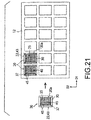
- the respective deposition masks 20 are stretched, and are aligned with respective openings of a frame 12 shown in Fig. 21 , for example, which has a grid-like plane shape, and are attached thereto, so as to manufacture a deposition mask 10 shown in Fig. 22 .
- Figs. 23 and 24 are views for describing yet another modification example of the manufacturing method of the deposition mask apparatus 10.
- Figs. 23 and 24 are plan views of respective members to show the respective steps of the deposition mask apparatus 10 in this modification example.
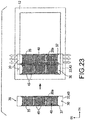
- each deposition mask 20 includes a first mask 30 having a plurality of openings 35 arranged along one direction (second direction D2), and has a general stick-like plane shape extending in the one direction.
- the respective deposition masks 20 are stretched and respectively attached to a frame 12 shown in Fig. 3 , for example, so as to manufacture a deposition mask apparatus 10 shown in Fig. 24 .
- the deposition mask 20 can be attached to the frame 12 similarly to the aforementioned attachment step.
- the deposition mask 20 having a stick-like plane shape can be stretched along the longitudinal direction (second direction D2), with only respective longitudinal ends of the deposition mask 20 being held by a plurality of clamps.
- the stretching step since the positions of the respective through-holes 45 can be corrected by stretching the deposition mask 20 along the longitudinal direction thereof, the stretching step can be facilitated.
- a notch and a joint piece which are similar to the notch 46 and the joint piece 48 described with reference to Figs. 6a and 7 , can be provided on the outer edges of the second masks 40 of the respective deposition masks 20.
- Fig. 25 is a partial plan view showing a modification example of the second mask 40 of the deposition mask 20.
- a plurality of notches 46 are arranged along a long side of the second mask 40 (along the first direction D1), and a width W 11 of each notch 46 along the long side is larger than the first width W 1 of the notch 46 in the embodiment described above with reference to Fig. 6 .
- the plurality of notches 46 and the joint pieces 48 arranged along the long side of the second mask 40 (along the first direction D1) have the width W 11 and a width W 12 , respectively.
- the plurality of notches 46 and the joint pieces 48 arranged along a short side of the second mask 40 (along the second direction D2) have a width W 11 and a width W 21 , respectively.
- the width W 11 is larger than the width W 21 .
- the width W 12 and the width W 22 may be the same with each other.
- a residual stress (internal stress) is generated in the metal layer 42, which results in a tensile force in the plane of the metal layer 42.
- a power of the tensile force varies depending on a thickness and/or a composition of the metal layer.
- a thickness of the joint piece 48 of the second mask 40 is set to be larger than a thickness of the porous area 44, in order to ensure an appropriate joint property.
- a larger in-plane tensile force may be generated in the joint piece 48 than in the porous area 44.
- the in-plane tensile force of the joint piece 48 can be reduced, whereby lowering of positional precision of the through-holes 45 in the porous area 44, which is caused by the in-plane tensile force, can be effectively prevented.
- Fig. 26 is a partial plan view showing another modification example of the second mask 40.
- a plurality of notches 46 are arranged along a long side of the second mask 40 (along the first direction D1), and a width W 11 of each notch 46 along the long side is larger than the first width W 1 of the notch 46 in the embodiment described above with reference to Fig. 6 .
- a plurality of notches 46 are arranged along a short side of the second mask 40 (along the second direction D2), and a width W 21 of each notch 46 along the short side is larger than the first width W 1 of the notch 46 in the embodiment described above with reference to Fig. 6 .
- the width W 11 and the width W 21 may be the same with each other, and the width W 12 and the width W 22 of may be the same with each other.
- Fig. 27 is a partial plan view showing yet another modification example of the second mask 40.
- a width W 112 of some notches 46 of a plurality of notches 46 arranged along a long side of the second mask 40 (along the first direction D1) is larger than a width W 111 of other notches 46.
- the width W 112 of every third notch 46 is larger than the other width W 111 of the notches 46.
- a width W 212 of some notches 46 of a plurality of notches 46 arranged along a short side of the second mask 40 (along the second direction D1) is larger than a width W 211 of other notches 46.
- the width W 212 of every third notch 46 is larger than the other width W 211 of the notches 46.
- the second mask 40 has a plurality of joint piece groups G arranged along its outer edge.
- One joint piece group G includes a plurality of joint pieces 48.
- one joint piece group G includes three joint pieces 48.
- Figs. 28 and 29 are partial plan view showing yet another modification example of the second mask 40.
- a width of a distal end 48a of a joint piece 48 is larger than a width of a proximal end 48b.
- the distal end 48 has a substantially circular outline in a plan view.
- the distal end 48a has a substantially rectangular outline in a plan view. Not limited to the substantially circular shape and the substantially rectangular shape, the distal end 48a can have any shape.
- the distal ends 48a can be joined to the first mask 30 by welding.
- the distal end 48a having relatively a larger width can ensure a suitably joint property to the first mask 30, and the proximal end 48b having relatively a smaller width can reduce the in-plane tensile force of the joint piece 48, whereby lowering of positional precision of the through-holes 45 in the porous area 44, which is caused by the in-plane tensile force, can be effectively prevented.
- Fig. 30 is a partial view showing yet another modification example of the second mask 40.
- a width of a joint piece 48 increases from a distal end side (end 49 side) toward a proximal end side (porous area 44 side).
- the joint piece 48 has a substantially trapezoidal outline in a plan view.
- the joint piece 48 has substantially an isosceles trapezoidal shape in a plan view.
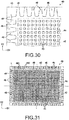
- Fig. 31 is a plan view showing yet another modification example of the second mask 40.
- a width of a joint piece 48 increases from the distal end side of the joint piece 48 toward the proximal end side thereof.
- the plurality of joint pieces 48 arranged along a long side of the second mask 40 and the plurality of joint pieces arranged along the long side of the second mask 40 have shapes different from each other, with respect to the center of the long side.
- the plurality of joint pieces 48 arranged along a short side of the second mask 40 and the plurality of joint pieces arranged along the short side of the second mask 40 have shapes different from each other, with respect to the center of the short side.
- the joint piece 48 has a substantially trapezoidal outline in a plan view, and has an end 49 and a proximal end, which form an upper base and a lower base of the trapezoidal shape, and two side edges 481, 482, which form legs of the substantially trapezoidal shape.
- the two side edges 481, 482 include a first side edge 481 facing a corner of the second mask 40 closest from the joint piece 48, and a second side edge 482 facing away from the corner.
- An angle defined between the second side edge 482 of the joint piece 48 and the outer edge 43 of the joint piece 48, which passes the end 49, is larger than an angle defined between the first side edge 481 of the joint piece 48 and the outer edge 43 of the joint piece 48, which passes the end 49 of the joint piece 48.
- the angle defined between the side edge 481, 482 and the outer edge 43 is greater than 0 degrees and not more than 90 degrees. Particularly in the illustrated example, the angle defined between the first side edge 481 and the outer edge 43 is 90 degrees, and the angle defined between the second side edge 482 and the outer edge 43 is less than 90 degrees.
- an in-plane tensile force in the metal layer 42 precipitated by a plating method acts relatively larger along a direction connecting a center of the second mask 40 and each corner thereof (diagonal direction).
- an angle defined between an orientation in which the joint piece 48 extends from its proximal end toward its distal end, and an orientation in which an in-plane tensile force in the metal layer 42 largely acts can be made smaller.
- an in-plane tensile force acting on the porous area 44 can be prevented from becoming non-uniform.
Landscapes
- Chemical & Material Sciences (AREA)
- Engineering & Computer Science (AREA)
- Chemical Kinetics & Catalysis (AREA)
- Organic Chemistry (AREA)
- Metallurgy (AREA)
- Mechanical Engineering (AREA)
- Materials Engineering (AREA)
- Manufacturing & Machinery (AREA)
- Physics & Mathematics (AREA)
- Condensed Matter Physics & Semiconductors (AREA)
- Power Engineering (AREA)
- Microelectronics & Electronic Packaging (AREA)
- Computer Hardware Design (AREA)
- General Physics & Mathematics (AREA)
- Inorganic Chemistry (AREA)
- General Chemical & Material Sciences (AREA)
- Optics & Photonics (AREA)
- Electroluminescent Light Sources (AREA)
- Physical Vapour Deposition (AREA)
Applications Claiming Priority (2)
| Application Number | Priority Date | Filing Date | Title |
|---|---|---|---|
| JP2017132162 | 2017-07-05 | ||
| PCT/JP2018/023065 WO2019009050A1 (fr) | 2017-07-05 | 2018-06-18 | Masque de dépôt en phase vapeur, dispositif de masque de dépôt en phase vapeur, procédé de fabrication de masque de dépôt en phase vapeur et procédé de fabrication de dispositif de masque de dépôt en phase vapeur |
Publications (2)
| Publication Number | Publication Date |
|---|---|
| EP3650575A1 true EP3650575A1 (fr) | 2020-05-13 |
| EP3650575A4 EP3650575A4 (fr) | 2021-04-21 |
Family
ID=64949937
Family Applications (1)
| Application Number | Title | Priority Date | Filing Date |
|---|---|---|---|
| EP18827999.6A Pending EP3650575A4 (fr) | 2017-07-05 | 2018-06-18 | Masque de dépôt en phase vapeur, dispositif de masque de dépôt en phase vapeur, procédé de fabrication de masque de dépôt en phase vapeur et procédé de fabrication de dispositif de masque de dépôt en phase vapeur |
Country Status (7)
| Country | Link |
|---|---|
| US (1) | US11380546B2 (fr) |
| EP (1) | EP3650575A4 (fr) |
| JP (1) | JP7008288B2 (fr) |
| KR (1) | KR102418174B1 (fr) |
| CN (2) | CN109207919B (fr) |
| TW (1) | TWI684653B (fr) |
| WO (1) | WO2019009050A1 (fr) |
Families Citing this family (14)
| Publication number | Priority date | Publication date | Assignee | Title |
|---|---|---|---|---|
| WO2019009050A1 (fr) | 2017-07-05 | 2019-01-10 | 大日本印刷株式会社 | Masque de dépôt en phase vapeur, dispositif de masque de dépôt en phase vapeur, procédé de fabrication de masque de dépôt en phase vapeur et procédé de fabrication de dispositif de masque de dépôt en phase vapeur |
| WO2020009088A1 (fr) * | 2018-07-03 | 2020-01-09 | 大日本印刷株式会社 | Masque et son procédé de production |
| WO2020158566A1 (fr) * | 2019-01-31 | 2020-08-06 | 大日本印刷株式会社 | Groupe de masques de dépôt, procédé de fabrication d'un dispositif électronique et dispositif électronique |
| JP7149196B2 (ja) * | 2019-02-01 | 2022-10-06 | 株式会社ジャパンディスプレイ | 蒸着マスク |
| KR20200096877A (ko) | 2019-02-06 | 2020-08-14 | 다이니폰 인사츠 가부시키가이샤 | 증착 마스크 장치, 마스크 지지 기구 및 증착 마스크 장치의 제조 방법 |
| CN109913805B (zh) * | 2019-03-27 | 2021-01-26 | 京东方科技集团股份有限公司 | 一种掩膜版 |
| JP7449485B2 (ja) * | 2019-03-28 | 2024-03-14 | 大日本印刷株式会社 | 蒸着マスク及び蒸着マスクの製造方法 |
| JP7473298B2 (ja) * | 2019-03-29 | 2024-04-23 | マクセル株式会社 | 蒸着マスク |
| CN111394692B (zh) * | 2020-05-09 | 2022-05-13 | 京东方科技集团股份有限公司 | 掩膜版 |
| KR20220056914A (ko) * | 2020-10-28 | 2022-05-09 | 삼성디스플레이 주식회사 | 마스크 프레임 및 이를 포함하는 증착 장치 |
| KR20220113588A (ko) * | 2021-02-05 | 2022-08-16 | 삼성디스플레이 주식회사 | 마스크 및 이의 제조 방법 |
| CN113005401A (zh) * | 2021-02-26 | 2021-06-22 | 昆山国显光电有限公司 | 张网方法及张网装置 |
| WO2023145950A1 (fr) * | 2022-01-31 | 2023-08-03 | 大日本印刷株式会社 | Masque de dépôt, masque de dépôt avec cadre, procédé de fabrication de masque de dépôt, procédé de fabrication de dispositif organique, et procédé de fabrication de masque de dépôt avec cadre |
| CN115948710A (zh) * | 2022-10-20 | 2023-04-11 | 京东方科技集团股份有限公司 | 一种蒸镀掩膜版及其制作方法、蒸镀设备 |
Family Cites Families (19)
| Publication number | Priority date | Publication date | Assignee | Title |
|---|---|---|---|---|
| JPH0885869A (ja) * | 1994-09-19 | 1996-04-02 | Murata Mfg Co Ltd | 電子部品の電極形成方法およびその方法に用いられるジグ |
| CA2426641C (fr) * | 2001-08-24 | 2010-10-26 | Dai Nippon Printing Co., Ltd. | Dispositif de masque de formation a plusieurs faces pour depot sous vide |
| JP4562488B2 (ja) | 2004-10-15 | 2010-10-13 | 大日本印刷株式会社 | メタルマスク位置アラインメント方法及び装置 |
| JP4606114B2 (ja) | 2004-10-15 | 2011-01-05 | 大日本印刷株式会社 | メタルマスク位置アラインメント方法及び装置 |
| JP2006124761A (ja) * | 2004-10-28 | 2006-05-18 | Canon Inc | 蒸着装置 |
| JP2005268822A (ja) * | 2005-05-27 | 2005-09-29 | Rohm Co Ltd | 半導体の電極形成方法及び蒸着用マスク |
| KR101202346B1 (ko) * | 2009-04-16 | 2012-11-16 | 삼성디스플레이 주식회사 | 박막 증착용 마스크 프레임 조립체, 그 제조 방법 및 유기 발광 표시 장치의 제조 방법 |
| KR20120105292A (ko) * | 2011-03-15 | 2012-09-25 | 삼성디스플레이 주식회사 | 증착 마스크 및 증착 마스크 제조 방법 |
| CN103781935B (zh) * | 2011-08-25 | 2017-07-11 | 应用材料公司 | 用以沉积层于基板上的遮罩结构、设备及方法 |
| US20160043319A1 (en) * | 2013-04-22 | 2016-02-11 | Applied Materials, Inc. | Actively-aligned fine metal mask |
| KR102218656B1 (ko) * | 2013-05-08 | 2021-02-23 | 삼성디스플레이 주식회사 | 마스크 조립체 및 이의 제조 방법 |
| JP5780350B2 (ja) * | 2013-11-14 | 2015-09-16 | 大日本印刷株式会社 | 蒸着マスク、フレーム付き蒸着マスク、及び有機半導体素子の製造方法 |
| JP6288497B2 (ja) * | 2013-12-13 | 2018-03-07 | 株式会社ブイ・テクノロジー | マスク及びその製造方法 |
| KR102474454B1 (ko) * | 2015-02-10 | 2022-12-06 | 다이니폰 인사츠 가부시키가이샤 | 증착 마스크의 제조 방법 및 증착 마스크 |
| KR102444178B1 (ko) * | 2015-04-27 | 2022-09-19 | 삼성디스플레이 주식회사 | 마스크 조립체, 마스크 조립체 제조방법 및 표시 장치 제조방법 |
| EP3358038B1 (fr) * | 2015-09-30 | 2023-01-18 | Dai Nippon Printing Co., Ltd. | Masque de dépôt, son procédé de fabrication et plaque métallique |
| CN106086781B (zh) * | 2016-06-15 | 2018-09-11 | 京东方科技集团股份有限公司 | 掩膜组件及其制造方法、显示装置 |
| JP7121918B2 (ja) * | 2016-12-14 | 2022-08-19 | 大日本印刷株式会社 | 蒸着マスク装置及び蒸着マスク装置の製造方法 |
| WO2019009050A1 (fr) * | 2017-07-05 | 2019-01-10 | 大日本印刷株式会社 | Masque de dépôt en phase vapeur, dispositif de masque de dépôt en phase vapeur, procédé de fabrication de masque de dépôt en phase vapeur et procédé de fabrication de dispositif de masque de dépôt en phase vapeur |
-
2018
- 2018-06-18 WO PCT/JP2018/023065 patent/WO2019009050A1/fr unknown
- 2018-06-18 KR KR1020207003256A patent/KR102418174B1/ko active IP Right Grant
- 2018-06-18 JP JP2019527608A patent/JP7008288B2/ja active Active
- 2018-06-18 EP EP18827999.6A patent/EP3650575A4/fr active Pending
- 2018-06-28 TW TW107122267A patent/TWI684653B/zh active
- 2018-07-05 CN CN201810729647.6A patent/CN109207919B/zh active Active
- 2018-07-05 CN CN201821059026.3U patent/CN208485938U/zh active Active
-
2019
- 2019-12-24 US US16/726,431 patent/US11380546B2/en active Active
Also Published As
| Publication number | Publication date |
|---|---|
| CN109207919B (zh) | 2020-12-08 |
| KR20200026280A (ko) | 2020-03-10 |
| CN109207919A (zh) | 2019-01-15 |
| JP7008288B2 (ja) | 2022-01-25 |
| US20200152463A1 (en) | 2020-05-14 |
| WO2019009050A1 (fr) | 2019-01-10 |
| CN208485938U (zh) | 2019-02-12 |
| KR102418174B1 (ko) | 2022-07-08 |
| US11380546B2 (en) | 2022-07-05 |
| TW201907029A (zh) | 2019-02-16 |
| EP3650575A4 (fr) | 2021-04-21 |
| TWI684653B (zh) | 2020-02-11 |
| JPWO2019009050A1 (ja) | 2020-04-30 |
Similar Documents
| Publication | Publication Date | Title |
|---|---|---|
| US11380546B2 (en) | Deposition mask, deposition mask apparatus, manufacturing method of deposition mask, and manufacturing method of deposition mask apparatus | |
| EP3556899B1 (fr) | Dispositif de masque de dépôt en phase vapeur et procédé de fabrication de dispositif de masque de dépôt en phase vapeur | |
| US11211558B2 (en) | Deposition mask device and method of manufacturing deposition mask device | |
| US11773477B2 (en) | Deposition mask | |
| EP3680362A1 (fr) | Procédé et dispositif de production pour dispositif de masque de dépôt en phase vapeur | |
| CN213232465U (zh) | 蒸镀掩模、蒸镀掩模装置以及中间体 | |
| JP2021147705A (ja) | 蒸着マスク装置の製造方法および有機el表示装置の製造方法 | |
| JP2020026553A (ja) | 蒸着マスク及び蒸着マスクの製造方法 | |
| EP3690078A1 (fr) | Masque de dépôt en phase vapeur | |
| JP2019081962A (ja) | 蒸着マスク | |
| JP6747054B2 (ja) | 蒸着マスク溶接方法 | |
| EP3674436B1 (fr) | Masque de dépôt | |
| JP2020084306A (ja) | 蒸着マスク装置の製造装置及び蒸着マスク装置の製造方法 | |
| JP7232430B2 (ja) | 蒸着マスクの製造方法 | |
| JP6425135B2 (ja) | 蒸着マスクの製造方法 | |
| JP3082805U (ja) | 蒸着用マスク | |
| JP7134589B2 (ja) | 蒸着マスク | |
| JP2021008673A (ja) | 蒸着マスク |
Legal Events
| Date | Code | Title | Description |
|---|---|---|---|
| STAA | Information on the status of an ep patent application or granted ep patent |
Free format text: STATUS: THE INTERNATIONAL PUBLICATION HAS BEEN MADE |
|
| PUAI | Public reference made under article 153(3) epc to a published international application that has entered the european phase |
Free format text: ORIGINAL CODE: 0009012 |
|
| STAA | Information on the status of an ep patent application or granted ep patent |
Free format text: STATUS: REQUEST FOR EXAMINATION WAS MADE |
|
| 17P | Request for examination filed |
Effective date: 20200109 |
|
| AK | Designated contracting states |
Kind code of ref document: A1 Designated state(s): AL AT BE BG CH CY CZ DE DK EE ES FI FR GB GR HR HU IE IS IT LI LT LU LV MC MK MT NL NO PL PT RO RS SE SI SK SM TR |
|
| AX | Request for extension of the european patent |
Extension state: BA ME |
|
| DAV | Request for validation of the european patent (deleted) | ||
| DAX | Request for extension of the european patent (deleted) | ||
| A4 | Supplementary search report drawn up and despatched |
Effective date: 20210319 |
|
| RIC1 | Information provided on ipc code assigned before grant |
Ipc: C23C 14/04 20060101AFI20210315BHEP Ipc: C23C 14/12 20060101ALI20210315BHEP Ipc: C23F 1/02 20060101ALI20210315BHEP |