EP3649635B1 - Oled-pixelschaltung sowie ansteuerungsverfahren dafür und anzeigevorrichtung - Google Patents
Oled-pixelschaltung sowie ansteuerungsverfahren dafür und anzeigevorrichtung Download PDFInfo
- Publication number
- EP3649635B1 EP3649635B1 EP17890839.8A EP17890839A EP3649635B1 EP 3649635 B1 EP3649635 B1 EP 3649635B1 EP 17890839 A EP17890839 A EP 17890839A EP 3649635 B1 EP3649635 B1 EP 3649635B1
- Authority
- EP
- European Patent Office
- Prior art keywords
- node
- voltage
- circuit
- data
- sub
- Prior art date
- Legal status (The legal status is an assumption and is not a legal conclusion. Google has not performed a legal analysis and makes no representation as to the accuracy of the status listed.)
- Active
Links
- 238000000034 method Methods 0.000 title claims description 42
- 238000005070 sampling Methods 0.000 claims description 62
- 239000003990 capacitor Substances 0.000 claims description 19
- 238000007667 floating Methods 0.000 claims description 7
- 238000010586 diagram Methods 0.000 description 8
- 230000000694 effects Effects 0.000 description 5
- 238000005516 engineering process Methods 0.000 description 3
- 230000001808 coupling effect Effects 0.000 description 2
- 230000003071 parasitic effect Effects 0.000 description 2
- 239000010409 thin film Substances 0.000 description 2
- 230000003679 aging effect Effects 0.000 description 1
- 230000005540 biological transmission Effects 0.000 description 1
- 238000004364 calculation method Methods 0.000 description 1
- 238000006243 chemical reaction Methods 0.000 description 1
- 230000008878 coupling Effects 0.000 description 1
- 238000010168 coupling process Methods 0.000 description 1
- 238000005859 coupling reaction Methods 0.000 description 1
- 238000001514 detection method Methods 0.000 description 1
- 239000004973 liquid crystal related substance Substances 0.000 description 1
- 239000011159 matrix material Substances 0.000 description 1
- 230000000750 progressive effect Effects 0.000 description 1
Images

Classifications
-
- G—PHYSICS
- G09—EDUCATION; CRYPTOGRAPHY; DISPLAY; ADVERTISING; SEALS
- G09G—ARRANGEMENTS OR CIRCUITS FOR CONTROL OF INDICATING DEVICES USING STATIC MEANS TO PRESENT VARIABLE INFORMATION
- G09G3/00—Control arrangements or circuits, of interest only in connection with visual indicators other than cathode-ray tubes
- G09G3/20—Control arrangements or circuits, of interest only in connection with visual indicators other than cathode-ray tubes for presentation of an assembly of a number of characters, e.g. a page, by composing the assembly by combination of individual elements arranged in a matrix no fixed position being assigned to or needed to be assigned to the individual characters or partial characters
- G09G3/22—Control arrangements or circuits, of interest only in connection with visual indicators other than cathode-ray tubes for presentation of an assembly of a number of characters, e.g. a page, by composing the assembly by combination of individual elements arranged in a matrix no fixed position being assigned to or needed to be assigned to the individual characters or partial characters using controlled light sources
- G09G3/30—Control arrangements or circuits, of interest only in connection with visual indicators other than cathode-ray tubes for presentation of an assembly of a number of characters, e.g. a page, by composing the assembly by combination of individual elements arranged in a matrix no fixed position being assigned to or needed to be assigned to the individual characters or partial characters using controlled light sources using electroluminescent panels
- G09G3/32—Control arrangements or circuits, of interest only in connection with visual indicators other than cathode-ray tubes for presentation of an assembly of a number of characters, e.g. a page, by composing the assembly by combination of individual elements arranged in a matrix no fixed position being assigned to or needed to be assigned to the individual characters or partial characters using controlled light sources using electroluminescent panels semiconductive, e.g. using light-emitting diodes [LED]
- G09G3/3208—Control arrangements or circuits, of interest only in connection with visual indicators other than cathode-ray tubes for presentation of an assembly of a number of characters, e.g. a page, by composing the assembly by combination of individual elements arranged in a matrix no fixed position being assigned to or needed to be assigned to the individual characters or partial characters using controlled light sources using electroluminescent panels semiconductive, e.g. using light-emitting diodes [LED] organic, e.g. using organic light-emitting diodes [OLED]
- G09G3/3225—Control arrangements or circuits, of interest only in connection with visual indicators other than cathode-ray tubes for presentation of an assembly of a number of characters, e.g. a page, by composing the assembly by combination of individual elements arranged in a matrix no fixed position being assigned to or needed to be assigned to the individual characters or partial characters using controlled light sources using electroluminescent panels semiconductive, e.g. using light-emitting diodes [LED] organic, e.g. using organic light-emitting diodes [OLED] using an active matrix
- G09G3/3233—Control arrangements or circuits, of interest only in connection with visual indicators other than cathode-ray tubes for presentation of an assembly of a number of characters, e.g. a page, by composing the assembly by combination of individual elements arranged in a matrix no fixed position being assigned to or needed to be assigned to the individual characters or partial characters using controlled light sources using electroluminescent panels semiconductive, e.g. using light-emitting diodes [LED] organic, e.g. using organic light-emitting diodes [OLED] using an active matrix with pixel circuitry controlling the current through the light-emitting element
-
- G—PHYSICS
- G09—EDUCATION; CRYPTOGRAPHY; DISPLAY; ADVERTISING; SEALS
- G09G—ARRANGEMENTS OR CIRCUITS FOR CONTROL OF INDICATING DEVICES USING STATIC MEANS TO PRESENT VARIABLE INFORMATION
- G09G3/00—Control arrangements or circuits, of interest only in connection with visual indicators other than cathode-ray tubes
- G09G3/20—Control arrangements or circuits, of interest only in connection with visual indicators other than cathode-ray tubes for presentation of an assembly of a number of characters, e.g. a page, by composing the assembly by combination of individual elements arranged in a matrix no fixed position being assigned to or needed to be assigned to the individual characters or partial characters
- G09G3/22—Control arrangements or circuits, of interest only in connection with visual indicators other than cathode-ray tubes for presentation of an assembly of a number of characters, e.g. a page, by composing the assembly by combination of individual elements arranged in a matrix no fixed position being assigned to or needed to be assigned to the individual characters or partial characters using controlled light sources
- G09G3/30—Control arrangements or circuits, of interest only in connection with visual indicators other than cathode-ray tubes for presentation of an assembly of a number of characters, e.g. a page, by composing the assembly by combination of individual elements arranged in a matrix no fixed position being assigned to or needed to be assigned to the individual characters or partial characters using controlled light sources using electroluminescent panels
- G09G3/32—Control arrangements or circuits, of interest only in connection with visual indicators other than cathode-ray tubes for presentation of an assembly of a number of characters, e.g. a page, by composing the assembly by combination of individual elements arranged in a matrix no fixed position being assigned to or needed to be assigned to the individual characters or partial characters using controlled light sources using electroluminescent panels semiconductive, e.g. using light-emitting diodes [LED]
- G09G3/3208—Control arrangements or circuits, of interest only in connection with visual indicators other than cathode-ray tubes for presentation of an assembly of a number of characters, e.g. a page, by composing the assembly by combination of individual elements arranged in a matrix no fixed position being assigned to or needed to be assigned to the individual characters or partial characters using controlled light sources using electroluminescent panels semiconductive, e.g. using light-emitting diodes [LED] organic, e.g. using organic light-emitting diodes [OLED]
-
- G—PHYSICS
- G09—EDUCATION; CRYPTOGRAPHY; DISPLAY; ADVERTISING; SEALS
- G09G—ARRANGEMENTS OR CIRCUITS FOR CONTROL OF INDICATING DEVICES USING STATIC MEANS TO PRESENT VARIABLE INFORMATION
- G09G2300/00—Aspects of the constitution of display devices
- G09G2300/08—Active matrix structure, i.e. with use of active elements, inclusive of non-linear two terminal elements, in the pixels together with light emitting or modulating elements
- G09G2300/0809—Several active elements per pixel in active matrix panels
- G09G2300/0819—Several active elements per pixel in active matrix panels used for counteracting undesired variations, e.g. feedback or autozeroing
-
- G—PHYSICS
- G09—EDUCATION; CRYPTOGRAPHY; DISPLAY; ADVERTISING; SEALS
- G09G—ARRANGEMENTS OR CIRCUITS FOR CONTROL OF INDICATING DEVICES USING STATIC MEANS TO PRESENT VARIABLE INFORMATION
- G09G2300/00—Aspects of the constitution of display devices
- G09G2300/08—Active matrix structure, i.e. with use of active elements, inclusive of non-linear two terminal elements, in the pixels together with light emitting or modulating elements
- G09G2300/0809—Several active elements per pixel in active matrix panels
- G09G2300/0842—Several active elements per pixel in active matrix panels forming a memory circuit, e.g. a dynamic memory with one capacitor
- G09G2300/0861—Several active elements per pixel in active matrix panels forming a memory circuit, e.g. a dynamic memory with one capacitor with additional control of the display period without amending the charge stored in a pixel memory, e.g. by means of additional select electrodes
-
- G—PHYSICS
- G09—EDUCATION; CRYPTOGRAPHY; DISPLAY; ADVERTISING; SEALS
- G09G—ARRANGEMENTS OR CIRCUITS FOR CONTROL OF INDICATING DEVICES USING STATIC MEANS TO PRESENT VARIABLE INFORMATION
- G09G2310/00—Command of the display device
- G09G2310/02—Addressing, scanning or driving the display screen or processing steps related thereto
- G09G2310/0202—Addressing of scan or signal lines
-
- G—PHYSICS
- G09—EDUCATION; CRYPTOGRAPHY; DISPLAY; ADVERTISING; SEALS
- G09G—ARRANGEMENTS OR CIRCUITS FOR CONTROL OF INDICATING DEVICES USING STATIC MEANS TO PRESENT VARIABLE INFORMATION
- G09G2310/00—Command of the display device
- G09G2310/02—Addressing, scanning or driving the display screen or processing steps related thereto
- G09G2310/0264—Details of driving circuits
- G09G2310/0294—Details of sampling or holding circuits arranged for use in a driver for data electrodes
-
- G—PHYSICS
- G09—EDUCATION; CRYPTOGRAPHY; DISPLAY; ADVERTISING; SEALS
- G09G—ARRANGEMENTS OR CIRCUITS FOR CONTROL OF INDICATING DEVICES USING STATIC MEANS TO PRESENT VARIABLE INFORMATION
- G09G2320/00—Control of display operating conditions
- G09G2320/02—Improving the quality of display appearance
- G09G2320/0233—Improving the luminance or brightness uniformity across the screen
-
- G—PHYSICS
- G09—EDUCATION; CRYPTOGRAPHY; DISPLAY; ADVERTISING; SEALS
- G09G—ARRANGEMENTS OR CIRCUITS FOR CONTROL OF INDICATING DEVICES USING STATIC MEANS TO PRESENT VARIABLE INFORMATION
- G09G2320/00—Control of display operating conditions
- G09G2320/02—Improving the quality of display appearance
- G09G2320/029—Improving the quality of display appearance by monitoring one or more pixels in the display panel, e.g. by monitoring a fixed reference pixel
- G09G2320/0295—Improving the quality of display appearance by monitoring one or more pixels in the display panel, e.g. by monitoring a fixed reference pixel by monitoring each display pixel
-
- G—PHYSICS
- G09—EDUCATION; CRYPTOGRAPHY; DISPLAY; ADVERTISING; SEALS
- G09G—ARRANGEMENTS OR CIRCUITS FOR CONTROL OF INDICATING DEVICES USING STATIC MEANS TO PRESENT VARIABLE INFORMATION
- G09G2320/00—Control of display operating conditions
- G09G2320/04—Maintaining the quality of display appearance
- G09G2320/043—Preventing or counteracting the effects of ageing
- G09G2320/045—Compensation of drifts in the characteristics of light emitting or modulating elements
-
- G—PHYSICS
- G09—EDUCATION; CRYPTOGRAPHY; DISPLAY; ADVERTISING; SEALS
- G09G—ARRANGEMENTS OR CIRCUITS FOR CONTROL OF INDICATING DEVICES USING STATIC MEANS TO PRESENT VARIABLE INFORMATION
- G09G2330/00—Aspects of power supply; Aspects of display protection and defect management
- G09G2330/02—Details of power systems and of start or stop of display operation
Definitions
- the present invention relates to display technology, more particularly, to a display apparatus including an organic light-emission display panel, and a method of driving pixel circuits included in the display apparatus.
- OLED display technology is popular today and is advantageous over Liquid Crystal Display (LCD) in low power consumption, selfluminous, wide viewing angle, and fast response speed.
- LCD Liquid Crystal Display
- OLED display panel has been applied in smart phone, PDA, digital camera to replace traditional LCD display panel.
- pixel circuit design plays an important role.
- OLED display panel is controlled by a driving current.
- a stable driving current is needed to control each light-emitting diode to emit light. Due to process variation and device aging effect, pixel luminance nonuniformity exists in the threshold voltage of each driving transistor in the pixel circuit. Additionally, the carrier mobility associated with the driving transistor is also drifted along with temperature variation. Therefore, even input image data are provided with a same gray scale level, the luminous level on the display panel still shows variation among different pixels, reducing the display effect of the whole image.
- US patent application US 2017/162122A1 discloses a gate driving circuit including a plurality of stages to respectively output a plurality of scan signals, an N-th stage of the stages includes: a shift register to output an N-th scan signal based on an (N-1)-th scan signal; and a sensing signal output block connected to the shift register and to output an (N-1)-th sensing signal for compensation of a pixel based on a sensing control signal and a data control signal, where N is an integer greater than 1.
- US patent application US 2013/147690 A1 discloses an organic light-emitting display device having a signal line that is shared by a first column of pixels and a second column of pixels to transmit a data signal and a sensing signal.
- the organic light-emitting display device includes a plurality of columns of pixels, and a plurality of signal lines extending between the plurality of columns of pixels. Each of the plurality of signal lines is configured to transmit a data signal from a data driver to the first column of pixels at first times.
- the data signals control the operation of an organic light-emitting element in the first column of pixels.
- the same signal line transmits a sensing signal from the second column of pixels to the data driver at second times.
- the sensing signal represents a variable property of an electrical component in a pixel of the second column of pixels.
- an organic light emitting display can include a display panel including a plurality of pixels of a source following manner, in which a source voltage of a driving thin film transistor (TFT) is changed according to a current flowing between a drain electrode and a source electrode of the driving TFT, a gate driving circuit for generating a mobility sensing gate pulse for operating the pixel in the source following manner, a data driving circuit for detecting a sensing voltage corresponding to mobility of the driving TFT from the pixel in response to the mobility sensing gate pulse, and a timing controller for setting a mobility sensing period in a period, in which a gate-source voltage of the driving TFT is greater than a threshold voltage of the driving TFT.
- TFT driving thin film transistor
- a so-called internal compensation is often used in certain designs of pixel circuit for generating a driving current that is able to compensate the drift of the threshold voltage of the driving transistor.
- conventional pixel circuit design with internal compensation can only compensate the threshold voltage drift in a relative small range while provide poor compensation to the carrier mobility.
- a so-called external compensation may be able to provide very good compensations to both the threshold voltage and carrier mobility of the driving transistor in the pixel circuit but has a major reliability drawback due to complicated circuit design, large volume of data processing, and prone to errors in the data processing and transmission.
- the present disclosure provides, inter alia, a pixel circuit, a method of driving the pixel circuit, an organic light-emitting diode (OLED) display panel, and a display apparatus having the same, that substantially obviate one or more of the problems due to limitations and disadvantages of the related art.
- OLED organic light-emitting diode
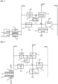
- FIG. 1 is a simplified block diagram of a pixel circuit according to some embodiments of the present disclosure.
- the block diagram shows that the pixel circuit includes at least a data-input sub-circuit 1, a driving-control sub-circuit 2, a reset sub-circuit 3, a power-storage sub-circuit 4, a light-emitting device 5, and a sampling sub-circuit 6 electrically coupled to at least a data line (Data), a reset line (Initial), several scan lines G1, G2, and G3, a first power supply Vdd and a second power supply Vss.
- Data data line
- Itial reset line
- G1, G2, and G3 a first power supply Vdd
- Vss second power supply
- the data input sub-circuit 1 is coupled to the data line Data, a first scan line G1, and a first node A of the pixel circuit.
- the data input sub-circuit 1 is configured to provide a data signal from the data line Data to the first node A under a control of a first control signal supplied from the first scan line G1.
- the reset sub-circuit 3 is coupled to the reset line Initial, a third scan line G3, and a second node B of the pixel circuit.
- the reset sub-circuit 3 is configured to provide a reset signal from the reset line Initial to the second node B under a control of a third control signal supplied from the third scan line G3.
- the driving-control sub-circuit 2 is coupled to the first power supply Vdd, the first node A, and the second node B.
- the driving-control circuit 2 is configured to drive the light-emitting device 5 to emit light under a control of a voltage at the first node A.
- the power-storage sub-circuit 4 is coupled to the first node A, the second node B, and is configured to regulate a voltage difference between the first node A and the second node B.
- the light-emitting device 5 is coupled to the second node B and the second power supply Vss.
- the sampling sub-circuit 6 is coupled to the data line Data, the second scan line G2, and the second node B.
- the sampling sub-circuit 6 is configured to connect the second node B to the data line Data under a control of the second control signal provided to the second scan line.
- the pixel circuit disclosed in FIG. 1 is able to perform an internal compensation to compensate a threshold voltage associated with a driving transistor in the driving-control sub-circuit 2. Additionally, the sampling sub-circuit 6 is able to connect the second node to the data line to allow a current signal be collected from the second node B which is depended upon the carrier mobility of the driving transistor.
- the pixel circuit of FIG. 1 also includes a first switch sub-circuit 7 coupled to the data line, and an ADC sub-circuit 8 coupled to the first switch sub-circuit 7. The first switch sub-circuit is turned on to allow the ADC sub-circuit 8 to receive the current signal.
- the ADC sub-circuit 8 is able to couple with an external processor to process the current signal and generate a compensation signal. Based on the compensation signal and original data signal for displaying a pixel image, a compensated data signal can be calculated.
- the pixel circuit of FIG. 1 also includes a DAC sub-circuit 10 coupled to a second switch sub-circuit 9 which is also coupled to the data line. The DAC sub-circuit 10 is configured to send the compensated data signal through the second switch sub-circuit 9 back to the data line for compensating the drift of the carrier mobility.
- the current signal collected from the data line corresponding to a voltage level at the second node contains information about other electrical properties beyond the carrier mobility associated with the driving transistor of the driving-control sub-circuit 2 as well as the light-emitting device 5. Therefore, the compensated data signal sent back from the DAC sub-circuit 10 is also able to properly compensate drifts or variations of those other electrical properties other than the carrier mobility.
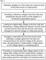
- the pixel circuit of FIG. 1 is given in more details in FIG. 2 .
- the driving-control sub-circuit 2 includes a driving transistor DT1 having a gate terminal coupled to the first node A, a source coupled to the first power supply Vdd, and a drain coupled to the second node B.
- the driving transistor DT1 is an N-type transistor.
- the first power supply Vdd provides a positive voltage
- the second power supply Vss provides a negative voltage or is simply grounded.
- the data-input sub-circuit 1 includes a first switch transistor T1 having a gate terminal coupled to the first scan line G1, a source coupled to the data line Data, and a drain coupled to the first node A.
- the first switch transistor T1 is an N-type transistor which is in a conduction state (on-state) when the first scan line G1 is provided with the first control signal at a high-level voltage or is in a block state (off-state) when the first control signal is a low-level voltage.
- the first switch transistor T1 can be a P-type transistor and is operated by opposite polarity of the first control signal provided at the first scan line G1. When the first switch transistor is in an on-state, it allows a data signal to be passed through the first switch transistor T1 and applies a voltage corresponding to the data signal to the first node A.
- the sampling sub-circuit 6 includes a second switch transistor T2 having a gate terminal coupled to the second scan line G2, a source coupled to the second node B, and a drain coupled to the data line Data.
- the second switch transistor When the second switch transistor is turned on by a second control signal at a turn-on level provided to the second scan line G2, the data line and the second node B will be at the same voltage level.
- the voltage at the second node B contains information about the current electric properties such as the threshold voltage and carrier mobility of the driving transistor DT1.
- a voltage signal collected at the data line is equivalent to the voltage at the second node, thus, the voltage signal collected at the data line will be processed to achieve compensation to the carrier mobility of the driving transistor.
- the reset sub-circuit 3 includes a third switch transistor T3 having a gate coupled to the third scan line G3, a source coupled to the reset line Initial, and a drain coupled to the second node B.
- a reset voltage can be applied through the third switch transistor T3 to the second node B to reset the second node potential level.
- the power-storage sub-circuit 4 is a capacitor C1 having a first terminal coupled to the first node A and a second terminal coupled to the second node B.
- the capacitor C1 is used to regulate the voltage difference between the first node A and the second node B based on its charging and coupling function.
- the capacitor C1 is to maintain the voltage difference stable during certain period of display cycle.
- the capacitor C1 is able to maintain the voltage difference stable between the first node and the second node.
- the voltage level at the second node is changed accordingly.
- the light-emitting device 5 is an organic light-emitting diode (OLED) having a first electrode coupled to the second node B and a second electrode coupled to the second power supply Vss (or optionally a ground voltage).
- OLED organic light-emitting diode
- the OLED is driven by a current signal to emit light.
- the current signal is substantially determined by the driving transistor DT1 controlled by the voltage at the first node A and the voltage at the second node B.
- the first Switch sub-circuit 7 includes a fourth switch transistor T4 having a first terminal coupled to the data line Data, a second terminal coupled to the ADC sub-circuit 8, and a gate being controlled by a first select signal V1. If V1 is set to a turn-on level the fourth switch transistor is in a conduction state and if V1 is set to a turn-off level the fourth transistor is in a block state.
- the ADC sub-circuit 8 is an analogto-digital conversion circuit configured to convert an analog signal received from the data line through the fourth transistor T4 to a digital signal, and send the digital signal to an external processor (not shown) to process the digital signal to calculate a compensation voltage based on a compensation algorithm.
- the second Switch sub-circuit 9 includes a fifth switch transistor having a first terminal coupled to a DAC sub-circuit 10 and a second terminal coupled to the data line Data, and a gate being controlled by a second select signal V2.
- the DAC sub-circuit 10 is configured to, at a proper period depended on a control scheme, convert a digital signal to an analog voltage. If V2 is set to a turn-on level, the fifth switch transistor T5 will be in a conduction state to allow the current signal to pass from the DAC sub-circuit 10 to the data line.
- the analog voltage carries a compensated data signal that is deduced from a compensation voltage obtained by the processor and at least an original data voltage that was supposed to drive the light-emitting device to emit light normally for displaying a pixel image.
- the second, third, fourth, and fifth switch transistors mentioned above can be either a N-type transistor or a P-type transistor, which can be operated to achieve respective desired function at either on-state or off-state only by setting the corresponding turn-on level or turn-off level to an opposite polarity.
- all the transistors are N-type transistors.
- the turn-on level of the transistor is represented by a high voltage level, denoted by "1" and the turn-off level of the transistor is a low voltage level, denoted by "0".
- each switch transistor is a thin-film transistor.
- each switch transistor is a MOS transistor.
- the source and drain of each transistor can be interchanged or simply referred to the first terminal and the second terminal thereof.
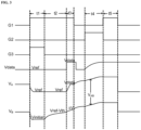
- a timing diagram of applying major control signals and setting corresponding voltages at data line and circuit nodes is provided in FIG. 3 in a single cycle of displaying one frame of (pixel) image.
- the single cycle includes at least five periods: a reset period 11, a threshold-compensation period t2, a first data-input period t3, a sampling period t4, and a second data-input period t5.
- the pixel circuit By executing various steps of controlling one or more sub-circuits in the pixel circuit in each of the five periods in certain order as depicted in the figure, the pixel circuit is able to drive the OLED to emit light with a proper emission intensity with both internal compensation and external compensation to eliminate potential electrical property drift effect associated with the driving transistor and the OLED itself.
- the timing diagram may include all the five periods but with some periods being in different orders relative to others.
- from one cycle to a next cycle there may be another gap time of variable duration.
- the driving transistor DT1, the first switch transistor T1, and the third switch transistor T3 are made to be a conduction state.
- the second switch transistor T2, the fourth switch transistor T4, and the fifth switch transistor T5 are turned off.
- the first node A and the second node B are respectively reset by a data signal Vdata (which is Vref) and a reset signal Vinitial.
- Vdata which is Vref
- Vinitial the data signal
- Vref is a reference voltage and not the original data voltage loaded to the data line when the pixel circuit is normally operated for displaying a pixel image.
- DT1, T1 are in conduction state.
- T2, T3, T4, and T5 are in block state.
- the first power supply Vdd through the DT1 in conduction state to charge the second node B until it reaches a first voltage level V B Vref - Vth, here Vth is a threshold voltage of the driving transistor DT1.
- Vdata is set to a same voltage level as in the reset period t1 for controlling the voltage level at first node A.
- DT1 and T1 are turned on and T2, T3, T4, and T5 are turned off.
- an original data signal set for displaying a pixel image with a desired intensity Vdata is loaded to the data line, which is in turn passed to the first node A.
- V A Vdata (or change from Vref in period t2 to Vdata in period t3).
- the OLED itself has an effective capacitance Coled.
- ⁇ V C1/(C1+Coled) ⁇ (Vdata - Vref).
- the storage capacitor C1 is configured to maintain the voltage difference V AB between the first node A and the second node B substantially stable.
- the voltage signal collected at the data line is received by the ADC sub-circuit 8 as an analog signal.
- the ADC sub-circuit 8 converts this analog signal to a digital signal and sent to an external processor.
- the processor is able to obtain a compensation voltage based on the second voltage at the second node.
- the obtained compensation voltage can be further used to generate a compensated data signal in accordance with an original data signal Vdata (per pixel circuit).
- the compensated data voltage once it is applied back to the data line, can make a proper compensation to substantially eliminate any drift effect of the threshold voltage and carrier mobility of the driving transistor DT1.
- the second voltage at the second node B which is also coupled to the first electrode of the OLED in the driving path from the first power supply Vdd to the second power supply Vss (or ground), is also affected by an IR drop across the OLED. Therefore, the compensated data signal obtained based on the current signal collected from the data line corresponding to the voltage level at the second node B is also able to provide a compensation of potential variation of IR drop of the OLED due to its electrical property drift.
- I represents a current flowing through the driving transistor
- C represents a parasitic capacitance of the data line which is a constant
- t represents a time duration of t4 period for the data line to be fully charged from the second node B.
- the current I is then changing with the variation of ⁇ U. Since the current I flowing through the driving transistor DT1 is proportional to the carrier mobility ⁇ n thereof, the voltage change ⁇ U on the data line can be used to deduce a compensation voltage for compensating the drift of the carrier mobility ⁇ n .
- V B Vref - Vth + ⁇ V at the second node B
- ⁇ V and Vref can be obtained by calculation.
- the voltage V B itself is sensed by the ADC sub-circuit 8. Therefore, in the above process, the value of threshold voltage Vth associated with the driving transistor currently in real time can also be captured.
- the driving transistor DT1, the first switch transistor T1, and the fifth switch transistor T5 are in conduction state.
- T2, T3, and T4 are turned off.
- T5 is turned on so that the compensated data signal can be converted to an analog compensated data voltage to be sent back to the data line. From the data line, the compensated data voltage is applied to the first node A to cause the driving transistor DT1 to determine a driving current I d flowing to the OLED.
- the driving current I d drives the OLED to emit light with a desired intensity the substantially eliminates drifts of electrical properties associated with the driving transistor as well as the OLED itself. Therefore, when different pixel circuits in a display panel receive a same original data signal, respect images can be displayed with a same luminance as each pixel circuit can be individually compensated to use corresponding compensated data signals to drive different pixel circuits for emitting light with potential different drifts being independently eliminated. This can substantially enhance image luminance uniformity in entire display area of the display panel.
- FIG. 4 shows an alternative example of applying major control signals and setting corresponding voltages at data line and circuit nodes according to a timing waveform for a single cycle of displaying a frame of pixel image.
- the cycle includes 6 periods of operating the pixel circuit: a node-reset period t1, a sampling period t2, a reset period t3, a threshold-compensation period t4, a data-input period t5, and an emission period t6.
- the operation of the pixel circuit includes the first two periods (t1 and t2) executed for an external compensation followed by four periods (t3 - t6) executed for an internal compensation.
- a compensated data signal obtained in the first two periods may be inputted immediately after the first two periods and may be inputted after one or more cycles during which only the internal compensations are performed.
- the pixel circuit of the present disclosure allows such flexibility of making proper external compensation less frequently to save a lot of time and power of the processor to process a huge amount of data for a plurality of pixel circuits (e.g., 3 ⁇ 1080 ⁇ 1920) in the OLED display panel.
- the driving transistor DT1, the first switch transistor T1, and the third switch transistor T3 are turned on in to a conduction state.
- the second switch transistor T2, the fourth switch transistor T4, and the fifth switch transistor T5 are turned off to be a block state.
- the data line is provided with a data signal which corresponds to a voltage of Vdata.
- the voltage Vdata is applied via the first switch transistor T1 to the first node A.
- V A Vdata.
- the reset line is provided with a reset signal Vinitial.
- This period is called no-reset period as both the first node A and the second node B are reset to respect voltages no matter what their previous voltage level is.
- the voltage Vdata is the same as an original data voltage supposed to be applied to the corresponding pixel circuit of the display panel through a progressive scanning-input scheme for displaying a frame of image. Of course, in this period, no current is yet generated to flow into the OLED to drive for light emission.
- the data line should be reset in a gap time to zero voltage and be a floating state.
- DT1 is still in conduction state as the voltage at the first node A remains at Vdata.
- the first node A is in floating state.
- T2 and T4 are turned on in this period.
- T1, T3, and T5 are turned off.
- the first power supply Vdd can charge the second node B to a first voltage higher than the previous level of Vinitial with a current I flown through the driving transistor DT1 in a duration of t.
- the first power supply Vdd can further charge the data line in the same duration of t to cause a change of voltage ⁇ U when T2 is in conduction state.
- T4 is turned on in this period to allow the voltage collected at the data line to be passed as an analog signal to the ADC sub-circuit 8.
- the ADC sub-circuit 8 is configured to convert the analog signal to a digital signal sent to an external processor to calculate a compensation voltage based on the first voltage at the second node B using a certain compensation algorithm.
- the compensation voltage calculated by the processor should bear all information for at least properly compensating the drift of carrier mobility.
- the current I also bears information about other electrical properties of the driving transistor as well as the OLED, both coupled to the second node.
- the compensation voltage should also be used for make compensation to drifts of the other electric properties of both the driving transistor and the OLED itself.
- the compensation voltage is used to generate a compensated data signal by the processor for a specific pixel circuit by considering an original data voltage supposed to apply to the pixel circuit before compensation.
- the compensated data signal is deduced after the sampling period t2 by the external processor.
- the compensated data signal is able to provide an external compensation to the driving current I d for driving the OLED to emit light with an intensity being substantially independent from at least the drift of carrier mobility of the driving transistor DT 1 as well as the drift of threshold voltage of DT 1 and variation of OLED itself.
- the compensated data signal is sent back to the data line as a compensated data voltage converted from a digital signal by a DAC sub-circuit 10 in an emission period after the sampling period t2.
- this compensated data voltage is loaded to the data line and can be passed to the first node A to control the driving transistor DT1 to generate a driving current I d to drive the OLED to emit light for completing the external compensation.
- this emission period may be executed once after one or more cycles of displaying one or more frames of images during which only internal compensation is performed to make the driving current I d to be independent from a threshold voltage Vth of the driving transistor DT1.
- the storage capacitor C1 is configured to maintain the voltage difference V AB between the first node A and the second node B substantially stable.
- T1, T2, T3, T4, and T5 all are turned off.
- an alternative emission period may include sending a compensated data signal determined by an external processor back to the data line to replace the original data voltage Vdata (as shown earlier after the sampling period t2), the drift effect of carrier mobility or other electric properties of the driving transistor as well the OLED in the pixel circuit can be compensated.
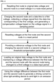
- FIG. 5 is a flow chart showing a method of driving the OLED pixel circuit of FIG. 2 according to an embodiment of the present disclosure. Referring to FIG.
- the method includes, in a reset period of the cycle, supplying the first control signal from the first scan line G1 to control the data-input sub-circuit 1 to connect the data line Data to the first node A; applying a reference voltage Vref from the data line Data to the first node A; supplying the third control signal from the third scan line G3 to control the reset sub-circuit 3 to connect the reset line Initial to the second node B; and applying a reset voltage Vinitial from the reset line to the second node B.
- the method further includes, in a threshold-compensation period of the cycle, supplying the first control signal from the first scan line G1 to control the data-input sub-circuit 1 o connect the data line Data to the first node A; using the reference voltage Vref at the first node A to make the driving-control sub-circuit 2 in conduction state; and using the first power supply Vdd through the driving-control sub-circuit 2 to charge the second node B to a first voltage equal to the reference voltage Vref minus a threshold voltage Vth associated with the driving-control sub-circuit 2.
- the method includes, in a data-input period of the cycle, supplying the first control signal from the first scan line G1 to control the data-input sub-circuit 1 to connect the data line Data to the first node A; applying an original data voltage Vdata from the data line to the first node A; and using the power-storage sub-circuit 4 to maintain a voltage difference V AB between the first node A and the second node B and change the second node B to a second voltage.
- the method further includes, in a sampling period, supplying the second control signal from the second scan line G2 to control the sampling sub-circuit 6 to connect the data line to the second node; using the first power supply Vdd through the driving-control sub-circuit 2 and the sampling sub-circuit 6 to charge the data line, collecting a voltage signal from the data line corresponding to the second voltage at the second node B to determine a compensation voltage based on the voltage signal.
- the method includes, in an emission period of the cycle, supplying the first control signal from the first scan line G1 to control the data-input sub-circuit 1 to connect the data line Data to the first node A; providing a compensated data voltage to the first node for controlling the driving-control sub-circuit 2 to determine a driving current I d flown from the first power supply Vdd through the driving-control sub-circuit 2 to drive the light-emitting device OLED to emit light.
- the driving current I d is independent from the threshold voltage Vth and carrier mobility ⁇ n drift.
- the method further includes, in the reset period, supplying the second control signal from the second scan line G2 to control the sampling sub-circuit 6 to disconnect the data line from the second node B; in the threshold-compensation period, supplying the second control signal from the second scan line G2 to control the sampling sub-circuit 6 to disconnect the data line Data from the second node B and supplying the third control signal from the third scan line G3 to control the reset sub-circuit 3 to disconnect the reset line Initial from the second node B.
- the method further includes, in the data-input period, using the original data voltage Vdata at the first node A to make the driving-control sub-circuit 2 in conduction state, supplying the second control signal from the second scan line G2 to control the sampling sub-circuit 6 to disconnect the data line Data from the second node B and supplying the third control signal from the third scan line G3 to control the reset sub-circuit 3 to disconnect the reset line Initial from the second node B to maintain the second node B at the second voltage.
- the method further includes, in the sampling period, supplying the first control signal from the first scan line G1 to control the data-input sub-circuit 1 to disconnect the data line from the first node A and supplying the third control signal from the third scan line G3 to control the reset sub-circuit 3 to disconnect the reset line Initial from the second node B.
- the method further includes, in the emission period, supplying the second control signal from the second scan line G2 to control the sampling sub-circuit 6 to disconnect the data line Data from the second node B and supplying the third control signal from the third scan line to control the reset sub-circuit 3 to disconnect the reset line from the second node B.
- the method further includes, after the data-input period and before the sampling period, supplying the first control signal G1 to disconnect the data line from the first node A to make the first node floating at the original data voltage to keep the driving-control sub-circuit 2 in conduction state, and resetting the data line Data to a zero voltage before being charged through the sampling sub-circuit 6 in the sampling period.
- the method of collecting a voltage signal from the data line corresponding to the second voltage at the second node to determine a compensation voltage includes supplying the first select signal at a turn-on level to turn the first switch sub-circuit to an on-state, sending the voltage signal to an ADC sub-circuit to convert the voltage signal to a digital signal, sending the digital signal to a processor to calculate a compensation voltage based on the second voltage at the second node and to calculate the compensated data voltage based on the compensation voltage and an original data voltage.
- the method of providing a compensated data voltage to the first node includes supplying the second select signal at a turn-on level to turn the second switch sub-circuit to an on-state, sending the compensated data voltage from an DAC sub-circuit to the data line through the data-input sub-circuit to the first node.
- FIG. 6 shows a flow chart showing a method of driving the OLED pixel circuit of FIG. 2 according to another embodiment of the present disclosure.
- the method of driving the pixel circuit in each cycle of displaying a frame of image includes, in the node-reset period, supplying the first control signal from the first scan line G1 to control the data-input sub-circuit 1 to connect the data line Data to the first node A, providing an original data voltage Vdata from the data line Data to the first node A, supplying the third control signal from the third scan line G3 to control the reset sub-circuit 3 to connect the reset line Initial to the second node B, providing the reset voltage Vinitial from the reset line to the second node B.
- the method further includes resetting the data line to zero voltage.
- the method further includes, in the sampling period, supplying the second control signal from the second scan line G2 to control the sampling sub-circuit 6 to connect the data line Data to the second node B, charging the data line Data from the first power supply Vdd through the driving-control sub-circuit 2 and the sampling sub-circuit 6 while charging the second node B to a first voltage, collecting a voltage signal from the data line Data corresponding to the first voltage at the second node B and to determine a compensation voltage based on the first voltage.
- the compensation voltage is calculated based on current electric properties associated with the driving-control sub-circuit 2 and the light-emitting device OLED and is used to determine a compensated data signal.
- the method includes, in the reset period, supplying the first control signal from the first scan line G1 to control the data-input sub-circuit 1 to connect the data line Data to the first node A; applying a reference voltage Vref from the data line Data to the first node A; supplying the third control signal from the third scan line G3 to control the reset sub-circuit 3 to connect the reset line Initial to the second node B; and applying a reset voltage Vinitial from the reset line to the second node B.
- the method further includes, in the threshold-compensation period, supplying the first control signal from the first scan line G1 to control the data-input sub-circuit 1 to connect the data line Data to the first node A; using the reference voltage Vref at the first node A to make the driving-control sub-circuit in conduction state; and using the first power supply Vdd through the driving-control sub-circuit 2 to charge the second node B to a second voltage equal to the reference voltage Vref minus a threshold voltage Vth associated with the driving-control sub-circuit 2.
- the method further includes, in the data-input period, supplying the first control signal from the first scan line G1 to control the data-input sub-circuit 1 to connect the data line Data to the first node A; applying an original data voltage Vdata from the data line Data to the first node A; and using the power-storage sub-circuit 4 to maintain a voltage difference V AB stable between the first node A and the second node B with the second node B being changed to a third voltage.
- the method includes, in the emission period, supplying all the first control signal, the second control signal, and the third control signal at turn-off level to disconnect the data line Data from the first node A and second node B and disconnect the reset line Initial from the second node B, using the voltage difference V AB between the first node A and the second node B maintained by the power-storage sub-circuit 4 to control the driving-control sub-circuit 2 to generate a driving current I d to drive the light-emitting device OLED to emit light.
- the driving current I d is at least independent from the threshold voltage Vth.
- the present disclosure provides an organic light-emission display panel including a plurality of pixel circuits arranged in a matrix.
- Each pixel circuit is a pixel circuit described herein and shown in FIG. 2 .
- the present disclosure provides a display apparatus including an organic light-emission display panel described above.
Landscapes
- Engineering & Computer Science (AREA)
- Physics & Mathematics (AREA)
- Computer Hardware Design (AREA)
- General Physics & Mathematics (AREA)
- Theoretical Computer Science (AREA)
- Control Of Indicators Other Than Cathode Ray Tubes (AREA)
- Control Of El Displays (AREA)
- Electroluminescent Light Sources (AREA)
Claims (13)
- Anzeigevorrichtung, eine organische Lichtemissions-Anzeigetafel aufweisend, wobei die organische Lichtemissions-Anzeigetafel mehrere Pixelschaltungen aufweist, wobei jede Pixelschaltung aufweist:eine Dateneingabe-Teilschaltung (1), die einen ersten Anschluss, der mit einer Datenleitung gekoppelt ist, einen zweiten Anschluss, der mit einer ersten Abtastleitung gekoppelt ist, die konfiguriert ist, um mit einem ersten Steuersignal versehen zu werden, einen dritten Anschluss, der mit einem ersten Knoten gekoppelt ist, hat und konfiguriert ist, um das erste Steuersignal zu verwenden, um das Anlegen einer Datenspannung von der Datenleitung an den ersten Knoten zu steuern;eine Rücksetz-Teilschaltung (3), die einen ersten Anschluss, der mit einer Rücksetzleitung gekoppelt ist, einen zweiten Anschluss, der mit einer dritten Abtastleitung gekoppelt ist, die konfiguriert ist, um mit einem dritten Steuersignal versehen zu werden, und einen dritten Anschluss, der mit einem zweiten Knoten gekoppelt ist, hat und konfiguriert ist, um das dritte Steuersignal zu verwenden, um das Anlegen einer Rücksetzspannung von der Rücksetzleitung an den zweiten Knoten zu steuern;einen Ansteuerungstransistor (2), der einen ersten Anschluss, der mit einer ersten Stromversorgung gekoppelt ist, einen zweiten Anschluss, der mit dem ersten Knoten gekoppelt ist, und einen dritten Anschluss, der mit dem zweiten Knoten gekoppelt ist, hat;einen Speicherkondensator (4), der einen ersten Anschluss, der mit dem ersten Knoten gekoppelt ist, und einen zweiten Anschluss, der mit dem zweiten Knoten gekoppelt ist, hat und konfiguriert ist, um eine Spannungsdifferenz zwischen dem ersten Knoten und dem zweiten Knoten zu regulieren;eine lichtemittierende Vorrichtung (5), die einen ersten Anschluss, der mit dem zweiten Knoten gekoppelt ist, und einen zweiten Anschluss, der mit einer zweiten Stromversorgung gekoppelt ist, hat; undeine Abtast-Teilschaltung (6), die einen ersten Anschluss, der mit der Datenleitung gekoppelt ist, einen zweiten Anschluss, der mit einer zweiten Abtastleitung gekoppelt ist, die konfiguriert ist, um mit einem zweiten Steuersignal versehen zu werden, und einen dritten Anschluss, der mit dem zweiten Knoten gekoppelt ist, hat und konfiguriert ist, um das zweite Steuersignal zu verwenden, um eine Verbindung des zweiten Knotens mit der Datenleitung zu steuern;wobei die organische Lichtemissions-Anzeigetafel ferner eine DAC-Teilschaltung (10) und eine zweite Schalt-Teilschaltung (9) aufweist, wobei die DAC-Teilschaltung (10) konfiguriert ist, um ein digitales Signal, das einer kompensierten Datenspannung zugeordnet ist, in ein analoges Spannungssignal umzuwandeln, und über die zweite Schalt-Teilschaltung (9) mit der Datenleitung gekoppelt ist, um das analoge Spannungssignal während einer Periode, in der sich die zweite Schalt-Teilschaltung (9) in einem Leitungszustand befindet, an die Datenleitung zu senden;dadurch gekennzeichnet, dass:in einer Rücksetzperiode (t1), die Anzeigevorrichtung konfiguriert ist, um: das erste Steuersignal von der ersten Abtastleitung zu liefern, um die Dateneingabe-Teilschaltung (1) zu steuern, so dass sie die Datenleitung mit dem ersten Knoten verbindet; eine Referenzspannung von der Datenleitung an den ersten Knoten anzulegen; das dritte Steuersignal von der dritten Abtastleitung zu liefern, um die Rücksetz-Teilschaltung (3) zu steuern, so dass sie die Rücksetzleitung mit dem zweiten Knoten verbindet; und die Rücksetzspannung von der Rücksetzleitung an den zweiten Knoten anzulegen;in einer Schwellenwertkompensationsperiode (t2), sich der Ansteuerungstransistor und die Dateneingabe-Teilschaltung (1) in dem Leitungszustand befinden, sich die Rücksetz-Teilschaltung (3) in dem Sperrzustand befindet und die Anzeigevorrichtung konfiguriert ist, um: das erste Steuersignal von der ersten Abtastleitung zu liefern, um die Dateneingabe-Teilschaltung (1) zu steuern, so dass sie die Datenleitung mit dem ersten Knoten verbindet; die Referenzspannung an dem ersten Knoten zu verwenden, um den Ansteuerungstransistor (2) in den Leitungszustand zu versetzen; und die erste Stromversorgung durch den Ansteuerungstransistor (2) zu verwenden, um den zweiten Knoten auf eine erste Spannung zu laden, die gleich der Referenzspannung minus der Schwellenspannung des Ansteuerungstransistors (2) ist;in einer ersten Dateneingabeperiode (t3), sich der Ansteuerungstransistor und die Dateneingabe-Teilschaltung (1) in dem Leitungszustand befinden, sich die Rücksetz-Teilschaltung (3) in dem Sperrzustand befindet und die Anzeigevorrichtung konfiguriert ist, um: das erste Steuersignal von der ersten Abtastleitung zu liefern, um die Dateneingabe-Teilschaltung (1) zu steuern, so dass sie die Datenleitung mit dem ersten Knoten verbindet; eine ursprüngliche Datenspannung von der Datenleitung an den ersten Knoten anzulegen; den zweiten Knoten auf eine zweite Spannung zu ändern; und dann den Speicherkondensator (4) zu verwenden, um eine Spannungsdifferenz zwischen dem ersten Knoten und dem zweiten Knoten stabil zu halten;in einer Abtastperiode (t4), die Anzeigevorrichtung konfiguriert ist, um: das zweite Steuersignal von der zweiten Abtastleitung zu liefern, um die Abtast-Teilschaltung (6) zu steuern, so dass sie die Datenleitung mit dem zweiten Knoten verbindet; die erste Stromversorgung durch den Ansteuerungstransistor (2) und die Abtast-Teilschaltung (6) zu verwenden, um die Datenleitung zu laden, ein Spannungssignal von der Datenleitung zu sammeln, das einer Spannung an dem zweiten Knoten entspricht, um eine Kompensationsspannung auf der Grundlage des Spannungssignals zu bestimmen; undin einer zweiten Dateneingabeperiode (t5), die Anzeigevorrichtung konfiguriert ist, um: das erste Steuersignal von der ersten Abtastleitung zu liefern, um die Dateneingabe-Teilschaltung (1) zu steuern, so dass sie die Datenleitung mit dem ersten Knoten verbindet; die kompensierte Datenspannung für den ersten Knoten vorzusehen, um den Ansteuerungstransistors (2) zu steuern, um einen Ansteuerungsstrom zu bestimmen, der von der ersten Stromversorgung durch den Ansteuerungstransistor (2) geschickt wird, wobei der Ansteuerungsstrom unabhängig von der Schwellenspannung und der Trägermobilitätsdrift ist;
oder,in einer Knoten-Rücksetzperiode (t1), die Anzeigevorrichtung konfiguriert ist, um: das erste Steuersignal von der ersten Abtastleitung zu liefern, um die Dateneingabe-Teilschaltung (1) zu steuern, so dass sie die Datenleitung mit dem ersten Knoten verbindet, eine ursprüngliche Datenspannung von der Datenleitung für den ersten Knoten vorzusehen, das dritte Steuersignal von der dritten Abtastleitung zu liefern, um die Rücksetz-Teilschaltung (3) zu steuern, so dass sie die Rücksetzleitung mit dem zweiten Knoten verbindet, die Rücksetzspannung von der Rücksetzleitung für den zweiten Knoten vorzusehen;in einer Abtastperiode (t2), die Anzeigevorrichtung konfiguriert ist, um: das zweite Steuersignal von der zweiten Abtastleitung liefern, um die Abtast-Teilschaltung (6) zu steuern, so dass sie die Datenleitung mit dem zweiten Knoten verbindet, die Datenleitung von der ersten Stromversorgung durch den Ansteuerungstransistor (2) und die Abtast-Teilschaltung (6), während der zweite Knoten auf eine erste Spannung geladen wird, zu laden, ein Spannungssignal von der Datenleitung, das der ersten Spannung an dem zweiten Knoten entspricht, zu sammeln und auf der Grundlage der ersten Spannung eine Kompensationsspannung zu bestimmen, wobei die Kompensationsspannung auf der Grundlage aktueller elektrischer Eigenschaften, die dem Ansteuerungstransistor (2) zugeordnet sind, berechnet wird und verwendet wird, um ein kompensiertes Datensignal zum Kompensieren der Trägermobilitätsdrift des Ansteuerungstransistors (2) zu bestimmen;in einer Rücksetzperiode (t3), die Anzeigevorrichtung konfiguriert ist, um: das erste Steuersignal von der ersten Abtastleitung zu liefern, um die Dateneingabe-Teilschaltung (1) zu steuern, so dass sie die Datenleitung mit dem ersten Knoten verbindet; eine Referenzspannung von der Datenleitung an den ersten Knoten anzulegen; das dritte Steuersignal von der dritten Abtastleitung zu liefern, um die Rücksetz-Teilschaltung (3) zu steuern, so dass sie die Rücksetzleitung mit dem zweiten Knoten verbindet; und die Rücksetzspannung von der Rücksetzleitung an den zweiten Knoten anzulegen;in einer Schwellenwertkompensationsperiode (t4), die Anzeigevorrichtung konfiguriert ist, um: das erste Steuersignal von der ersten Abtastleitung zu liefern, um die Dateneingabe-Teilschaltung (1) zu steuern, so dass sie die Datenleitung mit dem ersten Knoten verbindet; die Referenzspannung an dem ersten Knoten zu verwenden, um den Ansteuerungstransistor (2) in den Leitungszustand zu versetzen; und die erste Stromversorgung durch den Ansteuerungstransistor (2) zu verwenden, um den zweiten Knoten auf eine zweite Spannung zu laden, die gleich der Referenzspannung minus einer Schwellenspannung ist, die dem Ansteuerungstransistor (2) zugeordnet ist;in einer Dateneingabeperiode (t5), die Anzeigevorrichtung konfiguriert ist, um: das erste Steuersignal von der ersten Abtastleitung zu liefern, um die Dateneingabe-Teilschaltung (1) zu steuern, so dass sie die Datenleitung mit dem ersten Knoten verbindet; das kompensierte Datensignal als eine kompensierte Datenspannung durch die DAC-Teilschaltung (10) umzuwandeln, und die kompensierte Datenspannung von der Datenleitung an den ersten Knoten anzulegen; den zweiten Knoten auf eine dritte Spannung zu ändern; und dann den Speicherkondensator (4) zu verwenden, um eine Spannungsdifferenz zwischen dem ersten Knoten und dem zweiten Knoten stabil zu halten; undin einer Emissionsperiode (t6), die Anzeigevorrichtung konfiguriert ist, um: das erste Steuersignal, das zweite Steuersignal und das dritte Steuersignal allesamt auf Abschaltpegel zu liefern, um die Datenleitung von dem ersten Knoten und von dem zweiten Knoten zu trennen und die Rücksetzleitung von dem zweiten Knoten zu trennen, die Spannungsdifferenz zwischen dem ersten Knoten und dem zweiten Knoten, die durch den Speicherkondensator (4) aufrechterhalten wird, zu verwenden, um den Ansteuerungstransistors (2) zu steuern, so dass er einen Ansteuerungsstrom hervorbringt, um die lichtemittierende Vorrichtung (5) anzusteuern, so dass sie Licht emittiert, wobei der Ansteuerungsstrom unabhängig von der Schwellenspannung des Ansteuerungstransistors und der Trägermobilitätsdrift ist. - Anzeigevorrichtung nach Anspruch 1, wobei der Ansteuerungstransistor (2) ein Gate, das der zweite Anschluss des Ansteuerungstransistors (2) ist, der mit dem ersten Knoten gekoppelt ist, eine Source, die der erste Anschluss des Ansteuerungstransistors (2) ist, der mit der ersten Stromversorgung gekoppelt ist, und ein Drain, das der dritte Anschluss des Ansteuerungstransistors (2) ist, der mit dem zweiten Knoten gekoppelt ist, hat.
- Anzeigevorrichtung nach Anspruch 1, wobei die Dateneingabe-Teilschaltung (1) einen ersten Schalttransistor aufweist, der ein Gate, das der zweite Anschluss der Dateneingabe-Teilschaltung (1) ist, die mit der ersten Abtastleitung gekoppelt ist, eine Source, die der erste Anschluss der Dateneingabe-Teilschaltung (1) ist, die mit der Datenleitung gekoppelt ist, und ein Drain, das der dritte Anschluss der Dateneingabe-Teilschaltung (1) ist, die mit dem ersten Knoten gekoppelt ist, hat.
- Anzeigevorrichtung nach Anspruch 1, wobei die Abtast-Teilschaltung (6) einen zweiten Schalttransistor aufweist, der ein Gate, das der zweite Anschluss der Abtast-Teilschaltung (6) ist, die mit der zweiten Abtastleitung gekoppelt ist, eine Source, die der dritte Anschluss der Abtast-Teilschaltung (6) ist, die mit dem zweiten Knoten gekoppelt ist, und ein Drain, das der erste Anschluss der Abtast-Teilschaltung (6) ist, die mit der Datenleitung gekoppelt ist, hat.
- Anzeigevorrichtung nach Anspruch 1, wobei die Rücksetz-Teilschaltung (3) einen dritten Schalttransistor aufweist, der ein Gate, das der zweite Anschluss der Rücksetz-Teilschaltung (3) ist, die mit der dritten Abtastleitung gekoppelt ist, eine Source, die der erste Anschluss der Rücksetz-Teilschaltung (3) ist, die mit der Rücksetzleitung gekoppelt ist, und ein Drain, das der dritte Anschluss der Rücksetz-Teilschaltung (3) ist, die mit dem zweiten Knoten gekoppelt ist, hat.
- Anzeigevorrichtung nach Anspruch 1, wobei der Speicherkondensator (4) einen ersten Anschluss, der der erste Anschluss des Speicherkondensators (4) ist, der mit dem ersten Knoten gekoppelt ist, und einen zweiten Anschluss, der der zweite Anschluss des Speicherkondensators (4) ist, der mit dem zweiten Knoten gekoppelt ist, hat.
- Anzeigevorrichtung nach Anspruch 1, ferner eine ADC-Teilschaltung (8) und eine erste Schalt-Teilschaltung (7) aufweisend, wobei die ADC-Teilschaltung (8) über die erste Schalt-Teilschaltung (7) mit der Datenleitung gekoppelt ist und konfiguriert ist, um während einer Abtastperiode, wenn sich die erste Schalt-Teilschaltung (7) in dem Leitungszustand befindet, ein analoges Spannungssignal in der Datenleitung zu sammeln und das analoge Spannungssignal in ein digitales Signal umzuwandeln, das von einem Prozessor verwendet wird, um die kompensierte Datenspannung zu berechnen;wobei die erste Schalt-Teilschaltung (7) einen vierten Schalttransistor aufweist, der ein Gate, das durch ein erstes Auswahlsignal gesteuert wird, eine Source, die mit der Datenleitung gekoppelt ist, und ein Drain, das mit der ADC-Teilschaltung (8) gekoppelt ist, hat, wobei das erste Auswahlsignal konfiguriert ist, um auf einen Einschaltpegel gesetzt zu werden, um die erste Schalt-Teilschaltung (7) in den Leitungszustand zu versetzen;wobei die zweite Schalt-Teilschaltung (9) einen fünften Schalttransistor aufweist, der ein Gate, das durch ein zweites Auswahlsignal gesteuert wird, eine Source, die mit der DAC-Teilschaltung (10) gekoppelt ist, und ein Drain, das mit der Datenleitung gekoppelt ist, hat, wobei das zweite Auswahlsignal konfiguriert ist, um auf einen Einschaltpegel gesetzt zu werden, um die zweite Schalt-Teilschaltung (9) in den Leitungszustand zu versetzen.
- Verfahren zum Ansteuern einer Anzeigevorrichtung nach einem der Ansprüche 1 bis 7 in jedem Zyklus der Anzeige eines Bildes, wobei der Zyklus die Rücksetzperiode (t1), die Schwellenwertkompensationsperiode (t2), die erste Dateneingabeperiode (t3), die Abtastperiode (t4) und die zweite Dateneingabeperiode (t5) umfasst, wobei das Verfahren umfasst:in der Rücksetzperiode (t1), Liefern des ersten Steuersignals von der ersten Abtastleitung, um die Dateneingabe-Teilschaltung (1) zu steuern, so dass sie die Datenleitung mit dem ersten Knoten verbindet; Anlegen einer Referenzspannung von der Datenleitung an den ersten Knoten; Liefern des dritten Steuersignals von der dritten Abtastleitung, um die Rücksetz-Teilschaltung (3) zu steuern, so dass sie die Rücksetzleitung mit dem zweiten Knoten verbindet; und Anlegen der Rücksetzspannung von der Rücksetzleitung an den zweiten Knoten;in der Schwellenwertkompensationsperiode (t2), Liefern des ersten Steuersignals von der ersten Abtastleitung, um die Dateneingabe-Teilschaltung (1) zu steuern, so dass sie die Datenleitung mit dem ersten Knoten verbindet; Verwenden der Referenzspannung an dem ersten Knoten, um den Ansteuerungstransistor (2) in den Leitungszustand zu versetzen; und Verwenden der ersten Stromversorgung durch den Ansteuerungstransistor (2), um den zweiten Knoten auf eine erste Spannung zu laden, die gleich der Referenzspannung minus der Schwellenspannung des Ansteuerungstransistors (2) ist;in der ersten Dateneingabeperiode (t3), Liefern des ersten Steuersignals von der ersten Abtastleitung, um die Dateneingabe-Teilschaltung (1) zu steuern, so dass sie die Datenleitung mit dem ersten Knoten verbindet; Anlegen einer ursprünglichen Datenspannung von der Datenleitung an den ersten Knoten; Ändern des zweiten Knotens auf eine zweite Spannung, und dann Verwenden des Speicherkondensators (4), um eine Spannungsdifferenz zwischen dem ersten Knoten und dem zweiten Knoten stabil zu halten;in der Abtastperiode (t4), Liefern des zweiten Steuersignals von der zweiten Abtastleitung, um die Abtast-Teilschaltung (6) zu steuern, so dass sie die Datenleitung mit dem zweiten Knoten verbindet; Verwenden der ersten Stromversorgung durch den Ansteuerungstransistor (2) und der Abtast-Teilschaltung (6), um die Datenleitung zu laden, Sammeln eines Spannungssignals von der Datenleitung, das einer Spannung an dem zweiten Knoten entspricht, um auf der Grundlage des Spannungssignals eine Kompensationsspannung zu bestimmen; undin der zweiten Dateneingabeperiode (t5), Liefern des ersten Steuersignals von der ersten Abtastleitung, um die Dateneingabe-Teilschaltung (1) zu steuern, so dass sie die Datenleitung mit dem ersten Knoten verbindet; Vorsehen der kompensierten Datenspannung für den ersten Knoten zum Steuern des Ansteuerungstransistors (2), um einen Ansteuerungsstrom zu bestimmen, der von der ersten Stromversorgung durch den Ansteuerungstransistor (2) geschickt wird, wobei der Ansteuerungsstrom unabhängig von der Schwellenspannung und der Trägermobilitätsdrift ist.
- Verfahren nach Anspruch 8, ferner umfassend:in der Rücksetzperiode (t1), Liefern des zweiten Steuersignals von der zweiten Abtastleitung, um die Abtast-Teilschaltung (6) zu steuern, so dass sie die Datenleitung von dem zweiten Knoten trennt;in der Schwellenwertkompensationsperiode (t2), Liefern des zweiten Steuersignals von der zweiten Abtastleitung, um die Abtast-Teilschaltung (6) zu steuern, so dass sie die Datenleitung von dem zweiten Knoten trennt, und Liefern des dritten Steuersignals von der dritten Abtastleitung, um die Rücksetz-Teilschaltung (3) zu steuern, so dass sie die Rücksetzleitung von dem zweiten Knoten trennt;in der ersten Dateneingabeperiode (t3), Verwenden der ursprünglichen Datenspannung an dem ersten Knoten, um den Ansteuerungstransistor (2) in den Leitungszustand zu versetzen, Liefern des zweiten Steuersignals von der zweiten Abtastleitung, um die Abtast-Teilschaltung (6) zu steuern, so dass sie die Datenleitung von dem zweiten Knoten trennt, und Liefern des dritten Steuersignals von der dritten Abtastleitung, um die Rücksetz-Teilschaltung (3) zu steuern, so dass sie die Rücksetzleitung von dem zweiten Knoten trennt, um den zweiten Knoten auf der zweiten Spannung zu halten;in der Abtastperiode (t4), Liefern des ersten Steuersignals von der ersten Abtastleitung, um die Dateneingabe-Teilschaltung (1) zu steuern, so dass sie die Datenleitung von dem ersten Knoten trennt, und Liefern des dritten Steuersignals von der dritten Abtastleitung, um die Rücksetz-Teilschaltung (3) zu steuern, so dass sie die Rücksetzleitung von dem zweiten Knoten trennt; undin der zweiten Dateneingabeperiode (t5), Liefern des zweiten Steuersignals von der zweiten Abtastleitung, um die Abtast-Teilschaltung (6) zu steuern, so dass sie die Datenleitung von dem zweiten Knoten trennt, und Liefern des dritten Steuersignals von der dritten Abtastleitung, um die Rücksetz-Teilschaltung (3) zu steuern, so dass sie die Rücksetzleitung von dem zweiten Knoten trennt.
- Verfahren nach Anspruch 8, ferner nach der ersten Dateneingabeperiode (t3) und vor der Abtastperiode (t4) umfassend: Liefern des ersten Steuersignals von der ersten Abtastleitung, um die Datenleitung von dem ersten Knoten zu trennen, so dass der erste Knoten auf der ursprünglichen Datenspannung schwebt, um den Ansteuerungstransistor (2) in dem Leitungszustand zu halten, und Rücksetzen der Datenleitung auf eine Nullspannung, bevor sie in der Abtastperiode (t4) durch die Abtast-Teilschaltung (6) geladen wird;
wobei in der Abtastperiode (t4) das Sammeln eines Spannungssignals von der Datenleitung, das der zweiten Spannung an dem zweiten Knoten entspricht, um eine Kompensationsspannung zu bestimmen, ein Liefern des ersten Auswahlsignals auf einem Einschaltpegel umfasst, um die erste Schalt-Teilschaltung (7) in einen Ein-Zustand zu schalten, wobei das Spannungssignal an eine ADC-Teilschaltung (8) gesendet wird, um das Spannungssignal in ein digitales Signal umzuwandeln, wobei das digitale Signal an einen Prozessor gesendet wird, um eine Kompensationsspannung auf der Grundlage der zweiten Spannung an dem zweiten Knoten zu berechnen und die kompensierte Datenspannung auf der Grundlage der Kompensationsspannung und einer ursprünglichen Datenspannung zu berechnen. - Verfahren nach Anspruch 8, wobei in der zweiten Dateneingabeperiode (t5) das Vorsehen der kompensierten Datenspannung an den ersten Knoten ein Liefern des zweiten Auswahlsignals mit einem Einschaltpegel umfasst, um die zweite Schalt-Teilschaltung (9) in einen Ein-Zustand zu schalten, wobei die kompensierte Datenspannung von einer DAC-Teilschaltung (10) an die Datenleitung über die Dateneingabe-Teilschaltung (1) an den ersten Knoten gesendet wird.
- Verfahren zur Ansteuerung einer Anzeigevorrichtung nach einem der Ansprüche 1 bis 7 in jedem Zyklus der Anzeige eines Bildes, wobei der Zyklus die Knoten-Rücksetzperiode (t1), die Abtastperiode (t2), die Rücksetzperiode (t3), die Schwellenwertkompensationsperiode (t4), die Dateneingabeperiode (t5) und die Emissionsperiode (t6) umfasst, wobei das Verfahren umfasst:in der Knoten-Rücksetzperiode (t1), Liefern des ersten Steuersignals von der ersten Abtastleitung, um die Dateneingabe-Teilschaltung (1) zu steuern, so dass sie die Datenleitung mit dem ersten Knoten verbindet, Vorsehen einer ursprünglichen Datenspannung von der Datenleitung für den ersten Knoten, Liefern des dritten Steuersignals von der dritten Abtastleitung, um die Rücksetz-Teilschaltung (3) zu steuern, so dass sie die Rücksetzleitung mit dem zweiten Knoten verbindet, Vorsehen der Rücksetzspannung von der Rücksetzleitung für den zweiten Knoten;in der Abtastperiode (t2), Liefern des zweiten Steuersignals von der zweiten Abtastleitung, um die Abtast-Teilschaltung (6) zu steuern, so dass sie die Datenleitung mit dem zweiten Knoten verbindet, Laden der Datenleitung von der ersten Stromversorgung durch den Ansteuerungstransistor (2) und die Abtast-Teilschaltung (6), während der zweite Knoten auf eine erste Spannung geladen wird, Sammeln eines Spannungssignals von der Datenleitung, das der ersten Spannung an dem zweiten Knoten entspricht, und um eine Kompensationsspannung auf der Grundlage der ersten Spannung zu bestimmen, wobei die Kompensationsspannung auf der Grundlage aktueller elektrischer Eigenschaften, die dem Ansteuerungstransistor (2) zugeordnet sind, berechnet wird und verwendet wird, um ein kompensiertes Datensignal zum Kompensieren der Trägermobilitätsdrift des Ansteuerungstransistors (2) zu bestimmen;in der Rücksetzperiode (t3), Liefern des ersten Steuersignals von der ersten Abtastleitung, um die Dateneingabe-Teilschaltung (1) zu steuern, so dass sie die Datenleitung mit dem ersten Knoten verbindet; Anlegen einer Referenzspannung von der Datenleitung an den ersten Knoten; Liefern des dritten Steuersignals von der dritten Abtastleitung, um die Rücksetz-Teilschaltung (3) zu steuern, so dass sie die Rücksetzleitung mit dem zweiten Knoten verbindet; und Anlegen der Rücksetzspannung von der Rücksetzleitung an den zweiten Knoten;in der Schwellenwertkompensationsperiode (t4), Liefern des ersten Steuersignals von der ersten Abtastleitung, um die Dateneingabe-Teilschaltung (1) zu steuern, so dass sie die Datenleitung mit dem ersten Knoten verbindet; Verwenden der Referenzspannung an dem ersten Knoten, um den Ansteuerungstransistor (2) in den Leitungszustand zu versetzen; und Verwenden der ersten Stromversorgung durch den Ansteuerungstransistor (2), um den zweiten Knoten auf eine zweite Spannung zu laden, die gleich der Referenzspannung minus einer Schwellenspannung ist, die dem Ansteuerungstransistor (2) zugeordnet ist;in der Dateneingabeperiode (t5), Liefern des ersten Steuersignals von der ersten Abtastleitung, um die Dateneingabe-Teilschaltung (1) zu steuern, so dass sie die Datenleitung mit dem ersten Knoten verbindet; Umwandeln des kompensierten Datensignals als eine kompensierte Datenspannung durch die DAC-Teilschaltung (10) und Anlegen der kompensierten Datenspannung von der Datenleitung an den ersten Knoten; Ändern des zweiten Knotens auf eine dritte Spannung; und dann Verwenden des Speicherkondensators (4), um eine Spannungsdifferenz zwischen dem ersten Knoten und dem zweiten Knoten stabil zu halten; undin der Emissionsperiode (t6), Liefern des ersten Steuersignals, des zweiten Steuersignals und des dritten Steuersignals allesamt auf Abschaltpegel, um die Datenleitung von dem ersten Knoten und dem zweiten Knoten zu trennen und die Rücksetzleitung von dem zweiten Knoten zu trennen, Verwenden der Spannungsdifferenz zwischen dem ersten Knoten und dem zweiten Knoten, die durch den Speicherkondensator (4) aufrechterhalten wird, um den Ansteuerungstransistor (2) zu steuern, so dass er einen Ansteuerungsstrom hervorbringt, um die lichtemittierende Vorrichtung (5) anzusteuern, so dass sie Licht emittiert, wobei der Ansteuerungsstrom unabhängig von der Schwellenspannung des Ansteuerungstransistors und der Trägermobilitätsdrift ist.
- Verfahren nach Anspruch 12, ferner umfassend:Liefern des ersten Steuersignals von der ersten Abtastleitung nach der Knoten-Rücksetzperiode (t1) und vor der Abtastperiode (t2), um die Datenleitung von dem ersten Knoten zu trennen, um den ersten Knoten auf der ursprünglichen Datenspannung schwebend zu machen, um den Ansteuerungstransistor (2) in dem Leitungszustand zu halten, und Rücksetzen der Datenleitung auf eine Nullspannung, bevor sie durch die Abtast-Teilschaltung (6) in der Abtastperiode (t2) geladen wird;wobei in der Abtastperiode (t2) das Laden der Datenleitung ein Liefern des ersten Steuersignals von der ersten Abtastleitung, um die Dateneingabe-Teilschaltung (1) zu steuern, so dass sie die Datenleitung von dem ersten Knoten trennt, um den ersten Knoten schwebend zu machen, und ein Liefern des dritten Steuersignals von der dritten Abtastleitung, um die Rücksetz-Teilschaltung (3) zu steuern, so dass sie die Rücksetzleitung von dem zweiten Knoten trennt, umfasst; oderwobei in der Abtastperiode (t2) das Sammeln eines Spannungssignals von der Datenleitung, das der ersten Spannung an dem zweiten Knoten entspricht, um eine Kompensationsspannung zu bestimmen, ein Liefern des ersten Auswahlsignals auf einem Einschaltpegel umfasst, um die erste Schalt-Teilschaltung (7) in einen Ein-Zustand zu schalten, wobei das Spannungssignal an eine ADC-Teilschaltung (8) gesendet wird, um das Spannungssignal in ein digitales Signal umzuwandeln, wobei das digitale Signal an einen Prozessor gesendet wird, um eine Kompensationsspannung auf der Grundlage der ersten Spannung an dem zweiten Knoten zu berechnen und die kompensierte Datenspannung auf der Grundlage der Kompensationsspannung und einer ursprünglichen Datenspannung zu berechnen;das Verfahren ferner in einer alternierenden Emissionsperiode umfasst: nach der Abtastperiode (t2) Liefern des ersten Steuersignals von der ersten Abtastleitung, um die Dateneingabe-Teilschaltung (1) zu steuern, so dass sie die Datenleitung mit dem ersten Knoten verbindet, Liefern des zweiten Auswahlsignals mit einem Einschaltpegel, um die zweite Schalt-Teilschaltung (9) in einen Ein-Zustand zu schalten, wobei die kompensierte Datenspannung von einer DAC-Teilschaltung (10) an die Datenleitung über die Dateneingabe-Teilschaltung (1) an den ersten Knoten gesendet wird, Verwenden der kompensierten Datenspannung, um den Ansteuerungstransistors (2) zu steuern, um einen Ansteuerungsstrom zu bestimmen, um die lichtemittierende Vorrichtung anzusteuern, so dass sie Licht emittiert, wobei der Ansteuerungsstrom unabhängig von elektrischen Eigenschaftsabweichungen ist, die dem Ansteuerungstransistor (2) und der lichtemittierenden Vorrichtung (5) zugeordnet sind.
Applications Claiming Priority (2)
| Application Number | Priority Date | Filing Date | Title |
|---|---|---|---|
| CN201710539317.6A CN109215569B (zh) | 2017-07-04 | 2017-07-04 | 一种像素电路、驱动方法及显示装置 |
| PCT/CN2017/112090 WO2019006957A1 (en) | 2017-07-04 | 2017-11-21 | PIXEL DELO CIRCUIT, CORRESPONDING ATTACK METHOD, AND DISPLAY APPARATUS |
Publications (3)
| Publication Number | Publication Date |
|---|---|
| EP3649635A1 EP3649635A1 (de) | 2020-05-13 |
| EP3649635A4 EP3649635A4 (de) | 2021-03-31 |
| EP3649635B1 true EP3649635B1 (de) | 2024-02-07 |
Family
ID=64950474
Family Applications (1)
| Application Number | Title | Priority Date | Filing Date |
|---|---|---|---|
| EP17890839.8A Active EP3649635B1 (de) | 2017-07-04 | 2017-11-21 | Oled-pixelschaltung sowie ansteuerungsverfahren dafür und anzeigevorrichtung |
Country Status (4)
| Country | Link |
|---|---|
| US (1) | US11114027B2 (de) |
| EP (1) | EP3649635B1 (de) |
| CN (1) | CN109215569B (de) |
| WO (1) | WO2019006957A1 (de) |
Families Citing this family (14)
| Publication number | Priority date | Publication date | Assignee | Title |
|---|---|---|---|---|
| CN108597450A (zh) * | 2018-04-26 | 2018-09-28 | 京东方科技集团股份有限公司 | 像素电路及其驱动方法、显示面板 |
| CN109584788A (zh) | 2019-01-22 | 2019-04-05 | 京东方科技集团股份有限公司 | 像素驱动电路、像素单元及驱动方法、阵列基板、显示装置 |
| CN109728068B (zh) * | 2019-02-28 | 2020-10-30 | 上海天马有机发光显示技术有限公司 | 一种阵列基板、其驱动方法及显示装置 |
| CN109754757B (zh) * | 2019-03-28 | 2020-11-06 | 京东方科技集团股份有限公司 | 像素驱动电路、显示装置及像素驱动方法 |
| CN110111727A (zh) | 2019-06-03 | 2019-08-09 | 京东方科技集团股份有限公司 | 一种像素驱动电路及其驱动方法、显示装置 |
| CN110223636B (zh) * | 2019-06-17 | 2021-01-15 | 京东方科技集团股份有限公司 | 像素驱动电路及其驱动方法、显示装置 |
| US11514844B2 (en) | 2019-09-12 | 2022-11-29 | Beijing Boe Technology Development Co., Ltd. | Pixel drive circuit, pixel unit, driving method, array substrate, and display apparatus |
| CN110956928B (zh) * | 2019-12-25 | 2021-04-30 | 厦门天马微电子有限公司 | 一种有机发光显示装置及其驱动方法 |
| CN114175139B (zh) * | 2020-05-13 | 2023-04-18 | 京东方科技集团股份有限公司 | 像素驱动方法、显示驱动方法和显示基板 |
| CN111540300A (zh) * | 2020-05-15 | 2020-08-14 | 昆山国显光电有限公司 | 像素驱动电路、方法及显示面板 |
| KR20220050591A (ko) * | 2020-10-16 | 2022-04-25 | 엘지디스플레이 주식회사 | 표시장치, 구동회로 및 구동방법 |
| CN114363542B (zh) * | 2021-12-24 | 2023-11-24 | 合肥维信诺科技有限公司 | 感光电路结构和光学器件 |
| CN115346473B (zh) * | 2022-05-25 | 2023-10-24 | 惠科股份有限公司 | 显示面板、驱动电路及驱动方法 |
| CN116312358A (zh) * | 2022-12-28 | 2023-06-23 | 惠科股份有限公司 | 像素驱动电路、像素驱动方法以及显示装置 |
Family Cites Families (31)
| Publication number | Priority date | Publication date | Assignee | Title |
|---|---|---|---|---|
| KR100703492B1 (ko) * | 2005-08-01 | 2007-04-03 | 삼성에스디아이 주식회사 | 데이터 구동회로와 이를 이용한 유기 발광 표시장치 |
| WO2007037269A1 (ja) * | 2005-09-27 | 2007-04-05 | Casio Computer Co., Ltd. | 表示装置及び表示装置の駆動方法 |
| KR100858615B1 (ko) * | 2007-03-22 | 2008-09-17 | 삼성에스디아이 주식회사 | 유기전계발광 표시장치 및 그의 구동방법 |
| KR100893482B1 (ko) * | 2007-08-23 | 2009-04-17 | 삼성모바일디스플레이주식회사 | 유기전계발광 표시장치 및 그의 구동방법 |
| US8405582B2 (en) * | 2008-06-11 | 2013-03-26 | Samsung Display Co., Ltd. | Organic light emitting display and driving method thereof |
| KR101073297B1 (ko) * | 2009-07-10 | 2011-10-12 | 삼성모바일디스플레이주식회사 | 유기전계발광 표시장치 및 그의 구동방법 |
| KR101147427B1 (ko) * | 2010-03-02 | 2012-05-22 | 삼성모바일디스플레이주식회사 | 유기 발광 표시 장치 및 그의 구동 방법 |
| US9236011B2 (en) * | 2011-08-30 | 2016-01-12 | Lg Display Co., Ltd. | Organic light emitting diode display device for pixel current sensing in the sensing mode and pixel current sensing method thereof |
| KR101362002B1 (ko) * | 2011-12-12 | 2014-02-11 | 엘지디스플레이 주식회사 | 유기발광 표시장치 |
| KR101493226B1 (ko) * | 2011-12-26 | 2015-02-17 | 엘지디스플레이 주식회사 | 유기 발광 다이오드 표시 장치의 화소 구동 회로의 특성 파라미터 측정 방법 및 장치 |
| KR101928379B1 (ko) * | 2012-06-14 | 2018-12-12 | 엘지디스플레이 주식회사 | 유기발광 다이오드 표시장치 및 그 구동방법 |
| KR102053444B1 (ko) * | 2013-11-06 | 2019-12-06 | 엘지디스플레이 주식회사 | 유기발광 표시장치와 그의 이동도 보상방법 |
| KR101688923B1 (ko) * | 2013-11-14 | 2016-12-23 | 엘지디스플레이 주식회사 | 유기발광표시장치 및 그 구동방법 |
| KR102085167B1 (ko) * | 2013-12-31 | 2020-03-06 | 엘지디스플레이 주식회사 | 유기발광다이오드 표시장치 및 그의 구동방법 |
| KR101597037B1 (ko) * | 2014-06-26 | 2016-02-24 | 엘지디스플레이 주식회사 | 구동소자의 전기적 특성 편차를 보상할 수 있는 유기발광 표시장치 |
| KR101577907B1 (ko) * | 2014-09-02 | 2015-12-16 | 엘지디스플레이 주식회사 | 유기발광 표시장치의 문턱전압 변화값 센싱 방법 |
| KR101577909B1 (ko) * | 2014-09-05 | 2015-12-16 | 엘지디스플레이 주식회사 | 유기발광 표시장치의 열화 센싱 방법 |
| KR102286641B1 (ko) * | 2014-09-11 | 2021-08-06 | 엘지디스플레이 주식회사 | 구동소자의 경시 변화로 인한 휘도 편차를 보상할 수 있는 유기발광 표시장치 |
| US9607549B2 (en) * | 2014-12-24 | 2017-03-28 | Lg Display Co., Ltd. | Organic light emitting diode display panel and organic light emitting diode display device |
| KR102458503B1 (ko) * | 2015-11-03 | 2022-10-26 | 엘지디스플레이 주식회사 | 원격 보상 서비스 제공 방법, 원격 보상 서비스 시스템, 유기발광표시장치 및 원격 보상 서버 |
| KR102595263B1 (ko) | 2015-12-04 | 2023-10-30 | 삼성디스플레이 주식회사 | 게이트 구동 회로 및 이를 포함하는 유기 발광 표시 장치 |
| CN105913801B (zh) | 2016-06-20 | 2018-08-07 | 上海天马有机发光显示技术有限公司 | 一种有机发光显示面板及其驱动方法 |
| KR102570976B1 (ko) * | 2016-11-25 | 2023-08-28 | 엘지디스플레이 주식회사 | 표시장치와 그 소자 특성 센싱 방법 |
| CN106531074B (zh) * | 2017-01-10 | 2019-02-05 | 上海天马有机发光显示技术有限公司 | 有机发光像素驱动电路、驱动方法以及有机发光显示面板 |
| CN107622754B (zh) * | 2017-09-22 | 2023-11-14 | 京东方科技集团股份有限公司 | 像素电路及其控制方法、显示基板、显示装置 |
| US10347182B2 (en) * | 2017-11-07 | 2019-07-09 | Shenzhen China Star Optoelectronics Semiconductor Display Technology Co., Ltd. | OLED display device |
| CN107799062B (zh) * | 2017-11-27 | 2019-08-13 | 合肥鑫晟光电科技有限公司 | 一种像素电路及其驱动方法、显示装置 |
| TWI649741B (zh) * | 2018-01-30 | 2019-02-01 | 友達光電股份有限公司 | 臨界電壓補償電路以及顯示面板 |
| KR102513528B1 (ko) * | 2018-07-16 | 2023-03-24 | 삼성디스플레이 주식회사 | 유기 발광 표시 장치 및 이의 구동 방법 |
| KR20200123694A (ko) * | 2019-04-22 | 2020-10-30 | 삼성전자주식회사 | 디스플레이 구동 회로 및 이의 동작 방법 |
| US11107410B2 (en) * | 2019-08-15 | 2021-08-31 | Hefei Boe Joint Technology Co., Ltd. | Pixel circuit and method of controlling the same, display panel and display device |
-
2017
- 2017-07-04 CN CN201710539317.6A patent/CN109215569B/zh active Active
- 2017-11-21 WO PCT/CN2017/112090 patent/WO2019006957A1/en active Application Filing
- 2017-11-21 US US16/063,932 patent/US11114027B2/en active Active
- 2017-11-21 EP EP17890839.8A patent/EP3649635B1/de active Active
Also Published As
| Publication number | Publication date |
|---|---|
| US20210201776A1 (en) | 2021-07-01 |
| CN109215569A (zh) | 2019-01-15 |
| EP3649635A1 (de) | 2020-05-13 |
| EP3649635A4 (de) | 2021-03-31 |
| CN109215569B (zh) | 2020-12-25 |
| US11114027B2 (en) | 2021-09-07 |
| WO2019006957A1 (en) | 2019-01-10 |
Similar Documents
| Publication | Publication Date | Title |
|---|---|---|
| EP3649635B1 (de) | Oled-pixelschaltung sowie ansteuerungsverfahren dafür und anzeigevorrichtung | |
| US9881552B2 (en) | Display device and method for driving same | |
| US10510294B2 (en) | Pixel driving circuit, method for driving the same and display device | |
| US9842546B2 (en) | Organic light emitting display device for improving a contrast ratio | |
| US10504440B2 (en) | Pixel circuit, driving method thereof, display panel and display apparatus | |
| US9761177B2 (en) | Organic light emitting display device | |
| US9390652B2 (en) | Organic light emitting display device and driving method thereof | |
| JP6138254B2 (ja) | 表示装置およびその駆動方法 | |
| US9041705B2 (en) | Organic light emitting display device | |
| US8854343B2 (en) | Display device and method for driving the same | |
| US20180357963A1 (en) | A pixel circuit, a method for driving the pixel circuit, and a display apparatus | |
| KR101443224B1 (ko) | 유기 발광 다이오드의 화소 구조 및 그것의 구동 방법 | |
| WO2015093097A1 (ja) | 表示装置およびその駆動方法 | |
| US20100045646A1 (en) | Display device and its driving method | |
| EP2383721A2 (de) | System und Ansteuerungsverfahren der Anzeige einer lichtemittierenden Aktivmatrix-Vorrichtung | |
| US9779659B2 (en) | Pixel architecture and driving method thereof | |
| US10614757B2 (en) | Flexible display device and method for detecting bending state thereof | |
| US11176882B2 (en) | Display device and method for driving same | |
| US20190355304A1 (en) | Display device | |
| CN109166522B (zh) | 像素电路、其驱动方法及显示装置 | |
| US9633599B2 (en) | Pixel circuit, display device including the same and driving method of the display device | |
| US11562699B2 (en) | Display device and method for driving the same | |
| US11386849B2 (en) | Light emitting display device and method of driving same | |
| US8570255B2 (en) | Pixel driving device, light emitting device and light emitting device driving control method | |
| US8289309B2 (en) | Inverter circuit and display |
Legal Events
| Date | Code | Title | Description |
|---|---|---|---|
| STAA | Information on the status of an ep patent application or granted ep patent |
Free format text: STATUS: UNKNOWN |
|
| STAA | Information on the status of an ep patent application or granted ep patent |
Free format text: STATUS: THE INTERNATIONAL PUBLICATION HAS BEEN MADE |
|
| PUAI | Public reference made under article 153(3) epc to a published international application that has entered the european phase |
Free format text: ORIGINAL CODE: 0009012 |
|
| STAA | Information on the status of an ep patent application or granted ep patent |
Free format text: STATUS: REQUEST FOR EXAMINATION WAS MADE |
|
| 17P | Request for examination filed |
Effective date: 20180717 |
|
| AK | Designated contracting states |
Kind code of ref document: A1 Designated state(s): AL AT BE BG CH CY CZ DE DK EE ES FI FR GB GR HR HU IE IS IT LI LT LU LV MC MK MT NL NO PL PT RO RS SE SI SK SM TR |
|
| AX | Request for extension of the european patent |
Extension state: BA ME |
|
| DAV | Request for validation of the european patent (deleted) | ||
| DAX | Request for extension of the european patent (deleted) | ||
| REG | Reference to a national code |
Ref country code: DE Ref legal event code: R079 Ref document number: 602017079057 Country of ref document: DE Free format text: PREVIOUS MAIN CLASS: G09G0003320000 Ipc: G09G0003323300 Ref legal event code: R079 Free format text: PREVIOUS MAIN CLASS: G09G0003320000 |
|
| A4 | Supplementary search report drawn up and despatched |
Effective date: 20210301 |
|
| RIC1 | Information provided on ipc code assigned before grant |
Ipc: G09G 3/3233 20160101AFI20210223BHEP |
|
| STAA | Information on the status of an ep patent application or granted ep patent |
Free format text: STATUS: EXAMINATION IS IN PROGRESS |
|
| 17Q | First examination report despatched |
Effective date: 20220324 |
|
| GRAP | Despatch of communication of intention to grant a patent |
Free format text: ORIGINAL CODE: EPIDOSNIGR1 |
|
| STAA | Information on the status of an ep patent application or granted ep patent |
Free format text: STATUS: GRANT OF PATENT IS INTENDED |
|
| INTG | Intention to grant announced |
Effective date: 20230502 |
|
| GRAJ | Information related to disapproval of communication of intention to grant by the applicant or resumption of examination proceedings by the epo deleted |
Free format text: ORIGINAL CODE: EPIDOSDIGR1 |
|
| STAA | Information on the status of an ep patent application or granted ep patent |
Free format text: STATUS: EXAMINATION IS IN PROGRESS |
|
| GRAP | Despatch of communication of intention to grant a patent |
Free format text: ORIGINAL CODE: EPIDOSNIGR1 |
|
| STAA | Information on the status of an ep patent application or granted ep patent |
Free format text: STATUS: GRANT OF PATENT IS INTENDED |
|
| INTC | Intention to grant announced (deleted) | ||
| INTG | Intention to grant announced |
Effective date: 20230904 |
|
| GRAS | Grant fee paid |
Free format text: ORIGINAL CODE: EPIDOSNIGR3 |
|
| GRAA | (expected) grant |
Free format text: ORIGINAL CODE: 0009210 |
|
| STAA | Information on the status of an ep patent application or granted ep patent |
Free format text: STATUS: THE PATENT HAS BEEN GRANTED |
|
| AK | Designated contracting states |
Kind code of ref document: B1 Designated state(s): AL AT BE BG CH CY CZ DE DK EE ES FI FR GB GR HR HU IE IS IT LI LT LU LV MC MK MT NL NO PL PT RO RS SE SI SK SM TR |
|
| REG | Reference to a national code |
Ref country code: GB Ref legal event code: FG4D |
|
| REG | Reference to a national code |
Ref country code: CH Ref legal event code: EP |
|
| REG | Reference to a national code |
Ref country code: DE Ref legal event code: R096 Ref document number: 602017079057 Country of ref document: DE |
|
| REG | Reference to a national code |
Ref country code: IE Ref legal event code: FG4D |
|
| REG | Reference to a national code |
Ref country code: LT Ref legal event code: MG9D |