EP3637618B1 - Analog/digital-umsetzer - Google Patents
Analog/digital-umsetzer Download PDFInfo
- Publication number
- EP3637618B1 EP3637618B1 EP19202069.1A EP19202069A EP3637618B1 EP 3637618 B1 EP3637618 B1 EP 3637618B1 EP 19202069 A EP19202069 A EP 19202069A EP 3637618 B1 EP3637618 B1 EP 3637618B1
- Authority
- EP
- European Patent Office
- Prior art keywords
- residue
- capacitor
- coupled
- digital
- analog
- Prior art date
- Legal status (The legal status is an assumption and is not a legal conclusion. Google has not performed a legal analysis and makes no representation as to the accuracy of the status listed.)
- Active
Links
Images


Classifications
-
- H—ELECTRICITY
- H03—ELECTRONIC CIRCUITRY
- H03M—CODING; DECODING; CODE CONVERSION IN GENERAL
- H03M1/00—Analogue/digital conversion; Digital/analogue conversion
- H03M1/06—Continuously compensating for, or preventing, undesired influence of physical parameters
- H03M1/08—Continuously compensating for, or preventing, undesired influence of physical parameters of noise
- H03M1/0854—Continuously compensating for, or preventing, undesired influence of physical parameters of noise of quantisation noise
-
- H—ELECTRICITY
- H03—ELECTRONIC CIRCUITRY
- H03M—CODING; DECODING; CODE CONVERSION IN GENERAL
- H03M1/00—Analogue/digital conversion; Digital/analogue conversion
- H03M1/12—Analogue/digital converters
- H03M1/34—Analogue value compared with reference values
- H03M1/38—Analogue value compared with reference values sequentially only, e.g. successive approximation type
- H03M1/46—Analogue value compared with reference values sequentially only, e.g. successive approximation type with digital/analogue converter for supplying reference values to converter
- H03M1/462—Details of the control circuitry, e.g. of the successive approximation register
-
- H—ELECTRICITY
- H03—ELECTRONIC CIRCUITRY
- H03M—CODING; DECODING; CODE CONVERSION IN GENERAL
- H03M1/00—Analogue/digital conversion; Digital/analogue conversion
- H03M1/12—Analogue/digital converters
- H03M1/124—Sampling or signal conditioning arrangements specially adapted for A/D converters
- H03M1/1245—Details of sampling arrangements or methods
-
- H—ELECTRICITY
- H03—ELECTRONIC CIRCUITRY
- H03M—CODING; DECODING; CODE CONVERSION IN GENERAL
- H03M1/00—Analogue/digital conversion; Digital/analogue conversion
- H03M1/12—Analogue/digital converters
- H03M1/34—Analogue value compared with reference values
- H03M1/38—Analogue value compared with reference values sequentially only, e.g. successive approximation type
- H03M1/46—Analogue value compared with reference values sequentially only, e.g. successive approximation type with digital/analogue converter for supplying reference values to converter
- H03M1/466—Analogue value compared with reference values sequentially only, e.g. successive approximation type with digital/analogue converter for supplying reference values to converter using switched capacitors
- H03M1/468—Analogue value compared with reference values sequentially only, e.g. successive approximation type with digital/analogue converter for supplying reference values to converter using switched capacitors in which the input S/H circuit is merged with the feedback DAC array
Definitions
- the present invention relates to analog-to-digital converters (ADCs).
- SAR ADCs uccessive approximation analog-to-digital converters
- SNR signal-to-noise ratio
- Comparator noise and quantization noise are typically the dominant noise sources limiting the SNR.
- noise-shaping SAR (NS-SAR) ADCs have become popular to increase SNR, which considerably reduce these two noise sources.
- a basic concept of SAR ADC is described in this paragraph.
- an input voltage V I is sampled onto a weighted capacitor array (capacitive digital-to-analog converter, abbreviated to CDAC).
- CDAC capacitor digital-to-analog converter
- a comparator operates according to the CDAC to change the digital signals controlling the CDAC.
- the capacitors within the CDAC are switched between several reference voltages to equalize the voltage levels at the positive and negative output terminals of the CDAC, and the digital representation of the input voltage V I is determined from the MSB (most significant bit) to the LSB (least significant bit).
- a residue voltage V R may still exist between the positive and negative output terminal of the CDAC after the successive approximation.
- a noise-shaping signal may be derived from the residue voltage V R for noise elimination.
- the comparator of the SAR ADC usually provides an additional differential input pair for subtraction of the noise-shaping signal. The additional differential input pair, however, may contribute extra thermal and kickback noise.
- the generation of the noise-shaping signal may involve a charge-sharing procedure.
- An active residue amplification (using an op amp) is usually used to maintain the residue amplitude, which consumes a lot of power.
- a passive solution (without the op amp)
- a gain ratio between the signal and residue input pairs of the SAR comparator is required, which results in a large-sized SAR comparator.
- the charge-sharing procedure may repeat and the SAR comparator may require more input pairs.
- extra timing slots are required for the charge-sharing procedure, which also limits the sampling rate of the NS-SAR ADC.
- a 13-bit noise shaping SAR-ADC with dual polarity digital calibration (2013-02-27 ) a residue sampling capacitor is introduced.
- a rail-to-rail noise-shaping non-binary SAR ADC (2017-01-23 ) a rail-to-rail buffer for noise-shaping is introduced.
- noise-shaping successive approximation analog-to-digital converter using a passive noise-shaping technique with 1-input-pair SAR comparator is introduced.
- the invention is defined by the claims.
- An analog-to-digital converter (ADC) in accordance with the present invention includes a digital-to-analog converter (DAC), a comparator, and a residue sampling and integration circuit.
- the DAC samples an input signal according to a first control signal.
- the comparator operates according to the DAC to change the first control signal controlling the DAC, and for generating digital representation of the input signal.
- the residue sampling and integration circuit is coupled between the DAC and the comparator, for sampling a residue voltage generated by the DAC and charge-sharing of the sampled residue voltage.
- the residue sampling and integration circuit includes a first integral capacitor and a first residue capacitor.
- the first integral capacitor is coupled between a first input terminal of the comparator and a first output terminal of the DAC. After the first residue capacitor samples a residue voltage generated by the DAC, the first residue capacitor is coupled to the first integral capacitor for charge-sharing of the residue voltage.
- the residue sampling and integration circuit further includes a second integral capacitor and a second residue capacitor.
- the second integral capacitor is coupled between a second input terminal of the comparator and a second output terminal of the DAC. After the second residue capacitor samples a value of the residue voltage, the second residue capacitor is coupled to the second integral capacitor for charge-sharing of the residue voltage.
- a top plate of the first residue capacitor is coupled to the first output terminal of the DAC and a bottom plate of the first residue capacitor is coupled to the second output terminal of the DAC.
- a top plate of the second residue capacitor is coupled to the second output terminal of the DAC and a bottom plate of the second residue capacitor is coupled to the first output terminal of the DAC.
- a top plate of the first integral capacitor is coupled to the first input terminal of the comparator and a bottom plate of the first integral capacitor is coupled to the first output terminal of the DAC.
- a top plate of the second integral capacitor is coupled to the second input terminal of the comparator and a bottom plate of the second integral capacitor is coupled to the second output terminal of the DAC.
- the top plate of the first residue capacitor is coupled to the top plate of the first integral capacitor and the bottom plate of the first residue capacitor is coupled to the bottom plate of the first integral capacitor.
- the second residue capacitor is coupled to the second integral capacitor for charge-sharing of the residue voltage, the top plate of the second residue capacitor is coupled to the top plate of the second integral capacitor and the bottom plate of the second residue capacitor is coupled to the bottom plate of the second integral capacitor.
- a first input sampling phase, a first analog-to-digital conversion phase, and a first residue sampling phase are arranged.
- the DAC samples the input voltage.
- the first analog-to-digital conversion phase the successive approximation is performed.
- the first residue sampling phase the first residue capacitor samples the residue voltage and the second residue capacitor samples the value of the residue voltage.
- the first residue sampling phase overlaps the first input sampling phase and the first analog-to-digital conversion phase without using additional timing slots.
- a second input sampling phase, a second analog-to-digital conversion phase, and a first residue integral phase are additionally arranged.
- the DAC samples the input voltage again.
- the successive approximation is performed again.
- the first residue integral phase the first residue capacitor is coupled to the first integral capacitor and the second residue capacitor is coupled to the second integral capacitor for charge-sharing of the residue voltage.
- the first residue integral phase overlaps the second input sampling phase and the second analog-to-digital conversion phase without using additional timing slots.
- the residue sampling and integration circuit further includes a third residue capacitor and a fourth residue capacitor, for Ping-Pong mode operations.
- the DAC operates at a stable common-mode voltage.
- the DAC operates at a changing common-mode voltage for single-side successive approximation.
- the ADC further includes an amplifier.
- the amplifier has input terminals coupled to the first output terminal and the second output terminal of the DAC, and has output terminals coupled to the first integral capacitor and the second integral capacitor.
- the first residue capacitor is formed by two capacitors connected in series with a connection terminal coupled to a direct current voltage
- the second residue capacitor is formed by two capacitors connected in series with a connection terminal coupled to the direct current voltage
- FIG. 1 depicts a NS-SAR ADC (noise-shaping successive approximation analog-to-digital converter) 100 in accordance with an exemplary embodiment of the present invention.
- NS-SAR ADC noise-shaping successive approximation analog-to-digital converter
- the NS-SAR ADC 100 includes a CDAC (capacitive digital-to-analog converter) 102, a comparator (as known as a SAR comparator) 104, a SAR logic unit 106 and a decoder 108.
- the CDAC 102 is a weighted capacitor array.
- an input sampling phase corresponding to a high status of the control signal CLKS
- an input voltage V I is sampled onto the weighted capacitor array (CDAC 102).
- the top plates (corresponding to terminals IP and IN) of the CDAC 102 are coupled to the comparator 104.
- a series of comparator outputs are generated and sent to the SAR logic unit 106. Accordingly, the SAR logic unit 106 switches the reference voltages coupled to the capacitors of the CDAC 102 to achieve the successive approximation between the two terminals IP and IN.
- the successive approximation controlled by the SAR logic unit 106 is decoded by the decoder 108.
- the NS-SAR ADC 100 includes a residue sampling and integration circuit 110.
- the residue sampling and integration circuit 110 includes a residue capacitor pair (C RP1 , C RN1 ), a residue capacitor pair (C RP2 , C RN2 ) and an integral capacitor pair (C INTP and CINTN).
- a residue voltage (V R ) between the two terminals IP and IN is sampled selectively by the residue capacitor pair (C RP1 , C RN1 ) or the residue capacitor pair (C RP2 , C RN2 ), and is integrated into the integral capacitor pair (C INTP and C INTN ) by charge sharing.
- the integral capacitor C INTP is configured between the terminal IP and positive input terminal '+' (or SP) of the comparator 104 with the top plate coupled to the positive input terminal '+' and the bottom plate coupled to the terminal IP.
- Another integral capacitor C INTN is configured between the terminal IN and negative input terminal '-'(or SN) of the comparator 104 with the top plate coupled to the negative input terminal '-' and the bottom plate coupled to the terminal IN.
- the residue capacitor pairs (C RP1 , C RN1 ) and (C RP2 , C RN2 ) are utilized in a Ping-Pong mode, switched according to control signals ⁇ 1 and ⁇ 2.
- the control signal ⁇ 1 is high and the control signal ⁇ 2 is low.
- the residue capacitors C RP1 and C RN1 are coupled in parallel between the terminals IP and IN in a reverse direction with respect to each other.
- the residue capacitor C RP1 samples the residue voltage V R and the capacitor C RN1 samples the negative value of the residue voltage V R .
- the top plate and the bottom plate of the residue capacitor C RP1 are coupled to the terminals IP and IN, respectively.
- the top plate and the bottom plate of the capacitor C RN1 are coupled to the terminals IN and IP, respectively.
- the residue capacitor pair (C RP2 , C RN2 )
- the previous residue voltage sampled in the residue capacitor C RP2 and the negative value of the previous residue voltage sampled in the capacitor C RN2 are coupled to the integral capacitors C INTP and C INTN for residue integral.
- the top plate and the bottom plate of the residue capacitor C RP2 are coupled to the top plate and the bottom plate of the integral capacitor C INTP , respectively.
- the top plate and the bottom plate of the capacitor C RN2 are coupled to the top plate and the bottom plate of the integral capacitor C INTN , respectively.
- the comparator 104 includes one input pair.
- the integral of the residue voltage is added to the voltages at the terminals IP and IN.
- the noise-shaping signal is directly compensated on the voltages retrieved from the terminals IP and IN.
- the comparator 104 does not require additional input pair for the subtraction of noise-shaping signal.
- FIG. 2 shows the connection of the residue capacitor pairs (C RP1 , C RN1 ) and (C RP2 , C RN2 ) when the control signal ⁇ 2 is high and the control signal ⁇ 1 is low.
- the residue capacitors C RP2 and C RN2 are coupled in parallel between the terminals IP and IN in a reverse direction with respect to each other.
- the residue capacitor C RP2 samples the residue voltage V R and the capacitor C RN2 samples the negative value of the residue voltage V R .
- the top plate and the bottom plate of the residue capacitor C RP2 are coupled to the terminals IP and IN, respectively.
- the top plate and the bottom plate of the capacitor C RN2 are coupled to the terminals IN and IP, respectively.
- the residue capacitors C RP1 and C RN1 are coupled to the integral capacitors C INTP and C INTN for residue integral.
- the top plate and the bottom plate of the residue capacitor C RP1 are coupled to the top plate and the bottom plate of the integral capacitor C INTP , respectively.
- the top plate and the bottom plate of the capacitor C RN1 are coupled to the top plate and the bottom plate of the integral capacitor C INTN , respectively.
- FIG. 1 and FIG. 2 show Ping-Pong switching of the residue capacitor pairs (C RP1 , C RN1 ) and (C RP2 , C RN2 ).
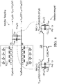
- FIG. 3 is a timing diagram of the control signals CLKS, CLKC, ⁇ 1 and ⁇ 2.
- the control signal CLKS is high, the input sampling phase for the input voltage V I is performed. Following the input sampling phase is the analog-to-digital conversion phase. As shown, the control signal CLKC oscillates during the analog-to-digital conversion phase. Without using any additional timing slots, the noise-shaping compensation including residue sampling and residue integral is performed during the input sampling phase and the analog-to-digital conversion phase. The sampling rate is improved.
- FIG. 3 there is a first input sampling phase 302, a first analog-to-digital conversion phase 304, a second input sampling phase 306 and a second analog-to-digital conversion phase 308.
- a residue sampling phase is implemented by the residue capacitor pair (C RP1 , C RN1 ) and a residue integral phase is implemented by the residue capacitor pair (C RP2 , C RN2 ), the two phases overlapping the first input sampling phase 302 and the first analog-to-digital conversion phase 304.
- a residue integral phase is implemented by the residue capacitor pair (C RP1 , C RN1 ) and a residue sampling phase is implemented by the residue capacitor pair (C RP2 , C RN2 ), the two phases overlapping the second input sampling phase 306 and the second analog-to-digital conversion phase 308. No additional timing slots are required for the residue sampling and residue integral.
- control signal ⁇ 1 is asserted after the control signal CLKS is asserted and prior to the oscillating of the control signal CLKC.
- the control signal ⁇ 1 is de-asserted before the next asserting of the control signal CLKC.
- the control signal ⁇ 2 is asserted after the asserting for the input sampling phase 306 and prior to the oscillating of the control signal CLKC, and is de-asserted before the next asserting of the control signal CLKC.
- FIG. 4 details the signals at the different circuit terminals.
- the residue component V RP (i) is V CM + ⁇ V R (i)/2.
- the residue component V RN (i) is V CM - ⁇ V R (i)/2.
- the residue capacitor pair (C RP , C RN ) is switched between residue sampling and residue integral.
- the residue voltage ⁇ V R (i) is captured by the residue capacitor pair (C RP , C RN ).
- the residue capacitors C RP and C RN are connected in parallel between the terminals IP and IN in opposite directions.
- the residue capacitor C RP samples a positive value of the residue voltage ⁇ V R (i) while the capacitor C RN samples a negative value of the residue voltage ⁇ V R (i).
- the residue capacitors C RP and C RN are connected to the positive and negative input terminals of the comparator 104, respectively.
- the sampled residue voltage ⁇ V R (i) is added to the positive input of the comparator 104, and subtracted from the negative input of the comparator 104.
- the output pair IP(i+1) and IN(i+1) of the CDAC 102 is also coupled to the same input pair SP(i+1) and SN(i+1) of the comparator 104 through the integral capacitor pairs (C INTP and C INTN ) and residue capacitor pairs (C RP , C RN ).
- the residue voltage ⁇ V R (i) is doubled without using any operational amplifier. And there is no need to use an additional comparator input pair with larger transistor size for the amplification of the residue voltage ⁇ V R (i).
- FIG. 5 is a block diagram depicting the transfer function of the NS-SAR ADC 100.
- the passive integration (capacitor sharing between C RES and C INT ) makes the factor a smaller than 1, where a is C RES /(C RES +C INT ).
- the sampled residue voltage is amplified without op amplifier or additional large-sized comparator input pair.
- D OUT z V I z + 1 ⁇ 05 Z ⁇ 1 / 1 + 05 Z ⁇ 1 Q z + V n , CMP z
- quantization error Q(z) and comparator error V n,CMP (z) are effectively suppressed.
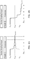
- the NS-SAR ADC 100 compensates for the noise according to the sampled residue voltage. Specifically, the residue voltage is sampled without the component of the common-mode voltage VCM. Thus, the NS-SAR ADC 100 is not only compatible with the successive approximation based on a stable common-mode voltage VCM as shown in ( FIG. 6A ), but also works well for successive approximation based on the changing common-mode voltage VCM ( FIG. 6B ).
- the CDAC 102 operates at a stable common mode voltage V CM . In another exemplary embodiment, the CDAC 102 operates at a changing common mode voltage V CM for single-side successive approximation.
- FIG. 7 depicts another residue sampling design in accordance with an exemplary embodiment of the present invention.
- An amplifier 702 is introduced to amplify the residue voltage between the two terminals IP and IN of the CDAC 102.
- FIG. 8 depicts another residue sampling design in accordance with an exemplary embodiment of the present invention.
- the residue sampling is further controlled by a direct current voltage VDC.
- each residue capacitor includes two capacitors (two residue capacitors 2C RP /two capacitors 2C RN ) connected in series with a connection terminal coupled to a direct current voltage VDC.
Landscapes
- Engineering & Computer Science (AREA)
- Theoretical Computer Science (AREA)
- Analogue/Digital Conversion (AREA)
Claims (7)
- Analog-Digital-Wandler (100), umfassend einen differentialen Digital-Analog-Kondensatorwandler (102) und einen Komparator (104), wobei Ausgangsanschlüsse des Digital-Analog-Kondensatorwandlers (102) mit dem Komparator (104) gekoppelt sind und der Digital-Analog-Kondensatorwandler (102) konfiguriert ist, um eine Eingangsspannung (VI) abzutasten, die ein Eingangssignal des Analog-Digital-Wandlers (100) ist, wobei der Digital-Analog-Kondensatorwandler (102) konfiguriert ist, um durch digitale Bits gesteuert zu werden, die basierend auf dem durch den Komparator (104) durchgeführten Vergleich erzeugt und betrieben werden, um sukzessive Approximationen basierend auf der abgetasteten Eingangsspannung durchzuführen, um eine digitale Darstellung (Dout) der Eingangsspannung (VI) an einem Ausgang des Analog-Digital-Wandlers zu erzeugen, wobei der Analog-Digital-Wandler (100) ferner umfasst:eine Restabtast- und Restintegrationsschaltung (110), die zwischen dem Digital-Analog-Kondensatorwandler (102) und dem Komparator (104) gekoppelt und konfiguriert ist, um eine durch den Digital-Analog-Kondensatorwandler (102) erzeugte Restspannung abzutasten und die abgetastete Restspannung ladungszuteilen, die Restabtast- und Restintegrationsschaltung (110) umfassend einen ersten integrierten Kondensator (CINTP), der zwischen einem ersten Eingangsanschluss (+) des Komparators (104) und einem ersten Ausgangsanschluss (IP) des Digital-Analog-Kondensatorwandlers (102) gekoppelt ist, und einen ersten Restkondensator (CRP1);die Restabtast- und Restintegrationsschaltung (110) ferner umfassend einen zweiten integrierten Kondensator (CINTN), der zwischen einem zweiten Eingangsanschluss (-) des Komparators (104) und einem zweiten Ausgangsanschluss (IN) des Digital-Analog-Kondensatorwandlers (102) gekoppelt ist, und einen zweiten Restkondensator (CRN1);wobei der Analog-Digital-Wandler ferner konfiguriert ist zum:nachdem der erste Restkondensator (CRP1) die durch den Digital-Analog-Kondensatorwandler (102) erzeugte Restspannung abgetastet hat, der erste Restkondensator (CRP1) mit dem ersten integrierten Kondensator (CINTP) gekoppelt ist, um die Restspannung ladungszuteilen; nachdem der zweite Restkondensator (CRN1) einen negativen Wert der Restspannung abgetastet hat, der zweite Restkondensator (CRN1) mit dem zweiten integrierten Kondensator (CINTN) gekoppelt ist, um den negativen Wert der Restspannung ladungszuteilen;während einer ersten Eingangsabtastphase (302) der Digital-Analog-Kondensatorwandler (102) die Eingangsspannung (VI) abtastet;während einer ersten Analog-Digital-Umwandlungsphase (304) die sukzessive Approximation durchgeführt wird;während einer ersten Restabtastphase der erste Restkondensator (CRP1) die Restspannung abtastet und der zweite Restkondensator (CRN1) den negativen Wert der Restspannung abtastet und die erste Restabtastphase die erste Eingangsabtastphase (302) und die erste Analog-Digital-Umwandlungsphase (304) überlappt und sich innerhalb der ersten Eingangsabtastphase (302) und der ersten Analog-Digital-Umwandlungsphase (304) befindet;während einer zweiten Eingangsabtastphase (306), die der ersten Analog-Digital-Umwandlungsphase (304) folgt, der Digital-Analog-Kondensatorwandler (102) die Eingangsspannung (VI) erneut abtastet;während einer zweiten Analog-Digital-Umwandlungsphase (308), die der zweiten Eingangsabtastphase (306) folgt, die sukzessive Approximation erneut durchgeführt wird; undwährend einer ersten Restintegrationsphase, der erste Restkondensator (CRP1) mit dem ersten integrierten Kondensator (CINTP) gekoppelt ist und der zweite Restkondensator (CRN1) mit dem zweiten integrierten Kondensator (CINTN) gekoppelt ist und konfiguriert ist, um die Restspannung beziehungsweise den negativen Wert der Restspannung ladungszuteilen, und die erste Restintegrationsphase die zweite Eingangsabtastphase (306) und die zweite Umwandlungsphase (308) überlappt,wobei der Restabtast- und Restintegrationsschaltkreis (110) ferner umfasst:einen dritten Restkondensator (CRP2); undeinen vierten Restkondensator (CRN2),wobei der Analog-Digital-Wandler ferner konfiguriert ist zum:wenn der erste Restkondensator (CRP1) das Abtasten der Restspannung beendet und der zweite Restkondensator (CRN1) das Abtasten des negativen Werts der Restspannung beendet, der dritte Restkondensator (CRP2) geschaltet wird, um die Restspannung abzutasten, und der vierte Restkondensator (CRN2) geschaltet wird, um den negativen Wert der Restspannung abzutasten;wenn der erste Restkondensator (CRP1) zurückgeschaltet wird, um die Restspannung abzutasten, eine obere Platte des dritten Restkondensators (CRP2) mit dem ersten Eingangsanschluss (+) des Komparators (104) gekoppelt ist und eine untere Platte des dritten Restkondensators (CRP2) mit dem ersten Ausgangsanschluss (IP) des Digital-Analog-Kondensatorwandlers (102) gekoppelt ist;wenn der zweite Restkondensator (CRN1) zurückgeschaltet wird, um den negativen Wert der Restspannung abzutasten, eine obere Platte des vierten Restkondensators (CRN2) mit dem zweiten Eingangsanschluss (-) des Komparators (104) gekoppelt ist und eine untere Platte des vierten Restkondensators (CRN2) mit dem zweiten Ausgangsanschluss (IN) des Digital-Analog-Kondensatorwandlers (102) gekoppelt ist;wenn der dritte Restkondensator (CRP2) verwendet wird, um die Restspannung abzutasten, die obere Platte des dritten Restkondensators (CRP2) mit dem ersten Ausgangsanschluss (IP) des Digital-Analog-Kondensatorwandlers (102) gekoppelt ist und die untere Platte des dritten Restkondensators (CRP2) mit dem zweiten Ausgangsanschluss (IN) des Digital-Analog-Kondensatorwandlers (102) gekoppelt ist; undwenn der vierte Restkondensator (CRN2) verwendet wird, um den negativen Wert der Restspannung abzutasten, die obere Platte des vierten Restkondensators (CRN2) mit dem zweiten Ausgangsanschluss (IN) des Digital-Analog-Kondensatorwandlers (102) gekoppelt ist und die untere Platte des vierten Restkondensators (CRN2) mit dem ersten Ausgangsanschluss (IP) des Digital-Analog-Kondensatorwandlers (102) gekoppelt ist, wobei:wenn der erste Restkondensator verwendet wird, um die Restspannung abzutasten, eine obere Platte des ersten Restkondensators (CRP1) mit dem ersten Ausgangsanschluss IP des Digital-Analog-Kondensatorwandlers (102) gekoppelt ist und eine untere Platte des ersten Restkondensators (CRP1) mit dem zweiten Ausgangsanschluss (IN) des Digital-Analog-Kondensatorwandlers (102) gekoppelt ist; undwenn der zweite Restkondensator verwendet wird, um den negativen Wert in Bezug auf die Restspannung abzutasten, eine obere Platte des zweiten Restkondensators (CRN1) mit dem zweiten Ausgangsanschluss des Digital-Analog-Kondensatorwandlers (102) gekoppelt ist und eine untere Platte des zweiten Restkondensators (CRN1) mit dem ersten Ausgangsanschluss des Digital-Analog-Wandlers (102) gekoppelt ist.
- Analog-Digital-Wandler nach Anspruch 1, wobei:eine obere Platte des ersten integrierten Kondensators (CINTP) mit dem ersten Eingangsanschluss (+) des Komparators (104) gekoppelt ist und eine untere Platte des ersten integrierten Kondensators (CINTP) mit dem ersten Ausgangsanschluss (IP) des Digital-Analog-Wandlers (102) gekoppelt ist;eine obere Platte des zweiten integrierten Kondensators (CINTP) mit dem zweiten Eingangsanschluss (-) des Komparators (104) gekoppelt ist und eine untere Platte des zweiten integrierten Kondensators (CINTN) mit dem zweiten Ausgangsanschluss (IN) des Digital-Analog-Kondensatorwandlers (102) gekoppelt ist;wenn der erste Restkondensator (CRP1) mit dem ersten integrierten Kondensator (CINTP) gekoppelt ist, der konfiguriert ist, um ladungszuteilen, die obere Platte des ersten Restkondensators (CRP1) mit der oberen Platte des ersten integrierten Kondensators (CINTP) gekoppelt ist und die untere Platte des ersten Restkondensators (CRP1) mit der unteren Platte des ersten integrierten Kondensators (CINTP) gekoppelt ist; undwenn der zweite Restkondensator (CRN1) mit dem zweiten integrierten Kondensator (CINTN) gekoppelt und konfiguriert ist, um ladungszuteilen, die obere Platte des zweiten Restkondensators (CRN1) mit der oberen Platte des zweiten integrierten Kondensators (CINTN) gekoppelt ist und die untere Platte des zweiten Restkondensators (CRN1) mit der unteren Platte des zweiten integrierten Kondensators (CINTN) gekoppelt ist.
- Analog-Digital-Wandler nach Anspruch 1, wobei:während einer zweiten Restabtastphase der dritte Restkondensator (CRP2) konfiguriert ist, um die Restspannung abzutasten, und der vierte Restkondensator (CRN2) konfiguriert ist, umden negativen Wert der Restspannung abzutasten; und die zweite Restabtastphase ferner konfiguriert ist, um die zweite Eingangsabtastphase (306) und die zweite Analog-Digital-Umwandlungsphase (308) zu überlappen und sich innerhalb der zweiten Eingangsabtastphase (306) und der zweiten Analog-Digital-Umwandlungsphase (308) zu befinden.
- Analog-Digital-Wandler nach Anspruch 3, der ferner konfiguriert ist zum:Abtasten der Eingangsspannung (VI) gemäß einem ersten Steuersignal (CLKS) in den Digital-Analog-Kondensatorwandler (102);Bringen des ersten Steuersignals (CLKS) in einen aktiven Zustand während der ersten Eingangsabtastphase (302) und der zweiten Eingabeabtastphase (306);Vergleichen von Signalen an dem ersten und dem zweiten Eingangsanschluss (+ und -) des Komparators (104), wenn ein zweites Steuersignal (CLKC) in den aktiven Zustand gebracht wird;Oszillieren des zweiten Steuersignals (CLKC) zwischen hoch und niedrig während der ersten Analog-Digital-Umwandlungsphase (304);Oszillieren des zweiten Steuersignals (CLKC) zwischen hoch und niedrig während der zweiten Analog-Digital-Umwandlungsphase (308);Starten der ersten Restabtastphase durch Bringen eines dritten Steuersignals (Φ1) in den aktiven Zustand und Beenden durch Bringen des dritten Steuersignals (Φ1) in einen nicht aktiven Zustand; undBringen des dritten Steuersignals (Φ1) in den aktiven Zustand nach einer ersten in-den-aktiven-Zustand-Bringung des ersten Steuersignals (CLKS) und vor einer Oszillation des zweiten Steuersignals (CLKS) und Bringen in den nicht aktiven Zusstand vor einer zweiten in-den-aktiven-Zustand-Bringung des ersten Steuersignals (CLKS).
- Analog-Digital-Wandler nach Anspruch 4, der ferner konfiguriert ist zum:Starten der zweiten Restabtastphase durch Bringen in den aktiven Zustand eines vierten Steuersignals (Φ2) und Beenden durch Bringen in den nicht aktiven Zustand des vierten Steuersignals (Φ2); undBringen des vierten Steuersignals (Φ2) in den aktiven Zustand nach der zweiten in-den-aktiven-Zustand-Bringung des ersten Steuersignals (CLKS) und vor der Oszillation des zweiten Steuersignals (CLKS) und Bringen in den nicht aktiven Zustand von diesem vor einer dritten in-den-aktiven-Zustand-Bringung des ersten Steuersignals (CLKS).
- Analog-Digital-Wandler nach einem der vorhergehenden Ansprüche, ferner umfassend:eine sukzessive-Approximation-Logikeinheit (106), die mit einem Ausgangsanschluss des Komparators gekoppelt ist, um die digitalen Bits zu erzeugen, die den Digital-Analog-Kondensatorwandler (102) gemäß dem Komparator (104) steuern; undeinen Decodierer (108), der konfiguriert ist, um gemäß der sukzessive-Approximation-Logikeinheit (106) zu decodieren und die digitale Darstellung (Dout) der Eingangsspannung (VI) zu erzeugen.
- Analog-Digital-Wandler nach einem der vorhergehenden Ansprüche, ferner umfassend:
einen Verstärker (702), der Eingangsanschlüsse aufweist, die mit dem ersten Ausgangsanschluss (IP) und dem zweiten Ausgangsanschluss (IN) des Digital-Analog-Kondensatorwandlers (102) gekoppelt sind, und der Ausgangsanschlüsse aufweist, die mit dem ersten integrierten Kondensator (CINTP) und dem zweiten integrierten Kondensator (CINTN) gekoppelt sind.
Applications Claiming Priority (2)
| Application Number | Priority Date | Filing Date | Title |
|---|---|---|---|
| US201862744705P | 2018-10-12 | 2018-10-12 | |
| US16/539,050 US10840932B2 (en) | 2018-10-12 | 2019-08-13 | Analog-to-digital converter |
Publications (2)
| Publication Number | Publication Date |
|---|---|
| EP3637618A1 EP3637618A1 (de) | 2020-04-15 |
| EP3637618B1 true EP3637618B1 (de) | 2023-01-11 |
Family
ID=68242386
Family Applications (1)
| Application Number | Title | Priority Date | Filing Date |
|---|---|---|---|
| EP19202069.1A Active EP3637618B1 (de) | 2018-10-12 | 2019-10-08 | Analog/digital-umsetzer |
Country Status (4)
| Country | Link |
|---|---|
| US (1) | US10840932B2 (de) |
| EP (1) | EP3637618B1 (de) |
| CN (1) | CN111049526B (de) |
| TW (1) | TWI695587B (de) |
Families Citing this family (7)
| Publication number | Priority date | Publication date | Assignee | Title |
|---|---|---|---|---|
| CN110113051B (zh) * | 2019-05-13 | 2020-03-31 | 深圳锐越微技术有限公司 | 模数转换器误差整形电路和逐次逼近型模数转换器 |
| JP7573236B2 (ja) * | 2020-09-28 | 2024-10-25 | パナソニックIpマネジメント株式会社 | Ad変換器、及びそれを備えるセンサシステム |
| CN113437976B (zh) * | 2021-04-09 | 2023-04-28 | 深圳市纽瑞芯科技有限公司 | 一种三态型量化的逐次逼近方法和逐次逼近模数转换电路 |
| US11522556B1 (en) * | 2021-07-26 | 2022-12-06 | Qualcomm Incorporated | Noise-shaping successive approximation register (SAR) analog-to-digital converter |
| CN115765745B (zh) * | 2022-11-22 | 2026-03-03 | 思瑞浦微电子科技(苏州)股份有限公司 | 混合型adc电路、芯片及模-数转换方法 |
| US12476648B2 (en) * | 2023-07-25 | 2025-11-18 | Cypress Semiconductor Corporation | Noise shaping successive-approximation register (SAR) analog-to-digital converter (ADC) |
| CN117938156B (zh) * | 2024-03-20 | 2024-06-18 | 华南理工大学 | 一种应用于ns sar adc的二阶噪声整形电路 |
Family Cites Families (23)
| Publication number | Priority date | Publication date | Assignee | Title |
|---|---|---|---|---|
| JP5178917B2 (ja) * | 2009-09-24 | 2013-04-10 | 株式会社東芝 | A/d変換装置、無線装置 |
| US8618975B2 (en) * | 2011-10-26 | 2013-12-31 | Semtech Corporation | Multi-bit successive approximation ADC |
| EP2629426A1 (de) * | 2012-02-17 | 2013-08-21 | Imec | Vorrichtung, System und Verfahren zur Analog-Digital-Umwandlung mit Rauschformungsfunktion |
| US9197240B1 (en) * | 2014-07-10 | 2015-11-24 | Taiwan Semiconductor Manufacturing Company, Ltd. | Method and circuit for noise shaping SAR analog-to-digital converter |
| CN106209104A (zh) * | 2015-05-27 | 2016-12-07 | 松下知识产权经营株式会社 | 模数转换器 |
| US9425818B1 (en) * | 2015-05-28 | 2016-08-23 | Qualcomm Incorporated | Noise shaping successive approximation register analog-to-digital converter |
| US9722746B2 (en) * | 2015-09-22 | 2017-08-01 | Mediatek Inc. | Analog-to-digital converter with bandpass noise transfer function |
| US20170126239A1 (en) * | 2015-11-04 | 2017-05-04 | Board Of Regents, The University Of Texas System | Noise-shaping successive-approximation-register analog-to-digital converter |
| JP2017168930A (ja) * | 2016-03-14 | 2017-09-21 | 株式会社東芝 | スイッチトキャパシタ回路 |
| US10340932B2 (en) * | 2016-04-29 | 2019-07-02 | Analog Devices, Inc. | Techniques for power efficient oversampling successive approximation register |
| WO2017195911A1 (ko) | 2016-05-10 | 2017-11-16 | 서강대학교 산학협력단 | 2차 노이즈 쉐이핑 기법을 적용한 sar adc |
| US10003348B2 (en) | 2016-09-08 | 2018-06-19 | Mediatek Inc. | Analog-to-digital converter with noise shaping |
| US9698805B1 (en) * | 2016-09-09 | 2017-07-04 | Analog Devices, Inc. | Electrical noise reduction in an analog-to-digital converter |
| US9774345B1 (en) * | 2016-09-20 | 2017-09-26 | Kabushiki Kaisha Toshiba | Successive approximation register analog-to-digital converter |
| US9973202B2 (en) * | 2016-09-20 | 2018-05-15 | Kabushiki Kaisha Toshiba | Successive approximation register analog-to-digital converter |
| JP6445746B2 (ja) * | 2016-12-21 | 2018-12-26 | オリンパス株式会社 | 逐次比較型a/d変換装置、撮像装置、内視鏡および設定方法 |
| JP6523577B2 (ja) * | 2016-12-21 | 2019-06-05 | オリンパス株式会社 | 撮像素子、撮像装置および内視鏡 |
| US10110242B2 (en) * | 2016-12-27 | 2018-10-23 | Mediatek Inc. | Interleaving successive approximation analog-to-digital converter with noise shaping |
| TWI653836B (zh) * | 2017-08-15 | 2019-03-11 | 瑞昱半導體股份有限公司 | 連續逼近式類比至數位轉換之校正裝置 |
| KR101840683B1 (ko) * | 2017-09-27 | 2018-03-21 | 포항공과대학교 산학협력단 | 잔류전압 적분을 이용한 축차 근사형 아날로그 디지털 변환기 |
| EP3503407B1 (de) * | 2017-12-19 | 2021-04-07 | IMEC vzw | Verbesserungen an oder im zusammenhang mit analog-digital-wandlern |
| US10547322B2 (en) * | 2018-01-02 | 2020-01-28 | Samsung Electronics Co., Ltd. | Analog-digital converter having multiple feedback, and communication device including the analog-digital converter |
| US10608655B1 (en) * | 2018-12-06 | 2020-03-31 | Analog Devices, Inc. | Inter-stage gain calibration in double conversion analog-to-digital converter |
-
2019
- 2019-08-13 US US16/539,050 patent/US10840932B2/en active Active
- 2019-09-25 CN CN201910913035.7A patent/CN111049526B/zh active Active
- 2019-09-27 TW TW108135106A patent/TWI695587B/zh active
- 2019-10-08 EP EP19202069.1A patent/EP3637618B1/de active Active
Also Published As
| Publication number | Publication date |
|---|---|
| US20200119744A1 (en) | 2020-04-16 |
| TW202015344A (zh) | 2020-04-16 |
| TWI695587B (zh) | 2020-06-01 |
| CN111049526A (zh) | 2020-04-21 |
| EP3637618A1 (de) | 2020-04-15 |
| CN111049526B (zh) | 2023-11-03 |
| US10840932B2 (en) | 2020-11-17 |
Similar Documents
| Publication | Publication Date | Title |
|---|---|---|
| EP3637618B1 (de) | Analog/digital-umsetzer | |
| Ramkaj et al. | A 1.25-GS/s 7-b SAR ADC with 36.4-dB SNDR at 5 GHz using switch-bootstrapping, USPC DAC and triple-tail comparator in 28-nm CMOS | |
| US9847790B2 (en) | Hybrid analog-to-digital converter using digital slope analog-to-digital converter and related hybrid analog-to-digital conversion method thereof | |
| US6784824B1 (en) | Analog-to-digital converter which is substantially independent of capacitor mismatch | |
| US9136867B2 (en) | ΔΣ-modulator and ΔΣ-A/D converter | |
| Hershberg et al. | A 4-GS/s 10-ENOB 75-mW ringamp ADC in 16-nm CMOS with background monitoring of distortion | |
| US20040061637A1 (en) | Sample-and-hold amplifier circuit and pipelined A/D and D/A converters using sample hold amplification circuit | |
| US20090073018A1 (en) | High Speed High Resolution ADC Using Successive Approximation Technique | |
| EP3567720B1 (de) | Fehlanpassungs- und referenzgleichtakt-offset-unempfindliche einseitig geschaltete kondensatorverstärkungsstufe | |
| US7075471B1 (en) | Double-sampled, time-interleaved analog to digital converter | |
| US7852254B1 (en) | 1-bit cell circuit used in a pipelined analog to digital converter | |
| Harpe | Low-power SAR ADCs: Basic techniques and trends | |
| EP3570436A1 (de) | Fehlanpassungs- und referenzgleichtaktversatzunempfindliche verstärkungsstufe für single-ended-kondensator mit reduzierter kondensatorfehlanpassungsempfindlichkeit | |
| US6756928B2 (en) | Pseudo-differential amplifier and analog-to-digital converter using the same | |
| CN101228696A (zh) | 模数转换器中的增益误差校正 | |
| JP4454498B2 (ja) | スイッチトキャパシタシステム、方法、および使用 | |
| Balasubramaniam et al. | 12-bit hybrid C2C DAC based SAR ADC with floating voltage shield | |
| Cho | A 2.24-mW, 61.8-dB SNDR, 20-MS/s pipelined ADC with charge-pump-based dynamic biasing for power reduction in op amp sharing | |
| Sigenobu et al. | An 8-bit 30 MS/s 18 mW ADC with 1.8 V single power supply | |
| JP4755249B2 (ja) | アナログデジタル変換器にける利得誤差補正 | |
| Dong et al. | An 11.36-Bit 405 μW SAR-VCO ADC with single-path differential VCO-based quantizer in 65 nm CMOS | |
| CN120110399B (zh) | 一种低功耗、用于连续时间δς模拟数字转换器的积分器 | |
| US20250365005A1 (en) | Integrator circuit | |
| KR101277558B1 (ko) | 레인지―스케일링 기법이 적용된 파이프라인 구조의 adc | |
| Tan et al. | A Design Method to Minimize the Impact of Bit Conversion Errors in SAR ADCs |
Legal Events
| Date | Code | Title | Description |
|---|---|---|---|
| PUAI | Public reference made under article 153(3) epc to a published international application that has entered the european phase |
Free format text: ORIGINAL CODE: 0009012 |
|
| STAA | Information on the status of an ep patent application or granted ep patent |
Free format text: STATUS: THE APPLICATION HAS BEEN PUBLISHED |
|
| AK | Designated contracting states |
Kind code of ref document: A1 Designated state(s): AL AT BE BG CH CY CZ DE DK EE ES FI FR GB GR HR HU IE IS IT LI LT LU LV MC MK MT NL NO PL PT RO RS SE SI SK SM TR |
|
| AX | Request for extension of the european patent |
Extension state: BA ME |
|
| STAA | Information on the status of an ep patent application or granted ep patent |
Free format text: STATUS: REQUEST FOR EXAMINATION WAS MADE |
|
| 17P | Request for examination filed |
Effective date: 20200814 |
|
| RBV | Designated contracting states (corrected) |
Designated state(s): AL AT BE BG CH CY CZ DE DK EE ES FI FR GB GR HR HU IE IS IT LI LT LU LV MC MK MT NL NO PL PT RO RS SE SI SK SM TR |
|
| STAA | Information on the status of an ep patent application or granted ep patent |
Free format text: STATUS: EXAMINATION IS IN PROGRESS |
|
| 17Q | First examination report despatched |
Effective date: 20220111 |
|
| RIC1 | Information provided on ipc code assigned before grant |
Ipc: H03M 1/46 20060101ALN20220516BHEP Ipc: H03M 1/08 20060101AFI20220516BHEP |
|
| RIC1 | Information provided on ipc code assigned before grant |
Ipc: H03M 1/46 20060101ALN20220711BHEP Ipc: H03M 1/08 20060101AFI20220711BHEP |
|
| GRAP | Despatch of communication of intention to grant a patent |
Free format text: ORIGINAL CODE: EPIDOSNIGR1 |
|
| STAA | Information on the status of an ep patent application or granted ep patent |
Free format text: STATUS: GRANT OF PATENT IS INTENDED |
|
| RIC1 | Information provided on ipc code assigned before grant |
Ipc: H03M 1/46 20060101ALN20220815BHEP Ipc: H03M 1/08 20060101AFI20220815BHEP |
|
| RIC1 | Information provided on ipc code assigned before grant |
Ipc: H03M 1/46 20060101ALN20220907BHEP Ipc: H03M 1/08 20060101AFI20220907BHEP |
|
| INTG | Intention to grant announced |
Effective date: 20220919 |
|
| RIC1 | Information provided on ipc code assigned before grant |
Ipc: H03M 1/46 20060101ALN20220909BHEP Ipc: H03M 1/08 20060101AFI20220909BHEP |
|
| GRAS | Grant fee paid |
Free format text: ORIGINAL CODE: EPIDOSNIGR3 |
|
| RIN1 | Information on inventor provided before grant (corrected) |
Inventor name: LU, CHAO HSIN Inventor name: TSOU, SHAN-CHIH Inventor name: TSAI, CHIHHOU Inventor name: LIN, CHIN-YU Inventor name: LIN, YING-ZU |
|
| GRAA | (expected) grant |
Free format text: ORIGINAL CODE: 0009210 |
|
| STAA | Information on the status of an ep patent application or granted ep patent |
Free format text: STATUS: THE PATENT HAS BEEN GRANTED |
|
| AK | Designated contracting states |
Kind code of ref document: B1 Designated state(s): AL AT BE BG CH CY CZ DE DK EE ES FI FR GB GR HR HU IE IS IT LI LT LU LV MC MK MT NL NO PL PT RO RS SE SI SK SM TR |
|
| REG | Reference to a national code |
Ref country code: GB Ref legal event code: FG4D |
|
| REG | Reference to a national code |
Ref country code: CH Ref legal event code: EP |
|
| REG | Reference to a national code |
Ref country code: DE Ref legal event code: R096 Ref document number: 602019024234 Country of ref document: DE |
|
| REG | Reference to a national code |
Ref country code: IE Ref legal event code: FG4D |
|
| REG | Reference to a national code |
Ref country code: AT Ref legal event code: REF Ref document number: 1544033 Country of ref document: AT Kind code of ref document: T Effective date: 20230215 |
|
| REG | Reference to a national code |
Ref country code: LT Ref legal event code: MG9D |
|
| REG | Reference to a national code |
Ref country code: NL Ref legal event code: MP Effective date: 20230111 |
|
| REG | Reference to a national code |
Ref country code: AT Ref legal event code: MK05 Ref document number: 1544033 Country of ref document: AT Kind code of ref document: T Effective date: 20230111 |
|
| PG25 | Lapsed in a contracting state [announced via postgrant information from national office to epo] |
Ref country code: NL Free format text: LAPSE BECAUSE OF FAILURE TO SUBMIT A TRANSLATION OF THE DESCRIPTION OR TO PAY THE FEE WITHIN THE PRESCRIBED TIME-LIMIT Effective date: 20230111 |
|
| P01 | Opt-out of the competence of the unified patent court (upc) registered |
Effective date: 20230607 |
|
| PG25 | Lapsed in a contracting state [announced via postgrant information from national office to epo] |
Ref country code: RS Free format text: LAPSE BECAUSE OF FAILURE TO SUBMIT A TRANSLATION OF THE DESCRIPTION OR TO PAY THE FEE WITHIN THE PRESCRIBED TIME-LIMIT Effective date: 20230111 Ref country code: PT Free format text: LAPSE BECAUSE OF FAILURE TO SUBMIT A TRANSLATION OF THE DESCRIPTION OR TO PAY THE FEE WITHIN THE PRESCRIBED TIME-LIMIT Effective date: 20230511 Ref country code: NO Free format text: LAPSE BECAUSE OF FAILURE TO SUBMIT A TRANSLATION OF THE DESCRIPTION OR TO PAY THE FEE WITHIN THE PRESCRIBED TIME-LIMIT Effective date: 20230411 Ref country code: LV Free format text: LAPSE BECAUSE OF FAILURE TO SUBMIT A TRANSLATION OF THE DESCRIPTION OR TO PAY THE FEE WITHIN THE PRESCRIBED TIME-LIMIT Effective date: 20230111 Ref country code: LT Free format text: LAPSE BECAUSE OF FAILURE TO SUBMIT A TRANSLATION OF THE DESCRIPTION OR TO PAY THE FEE WITHIN THE PRESCRIBED TIME-LIMIT Effective date: 20230111 Ref country code: HR Free format text: LAPSE BECAUSE OF FAILURE TO SUBMIT A TRANSLATION OF THE DESCRIPTION OR TO PAY THE FEE WITHIN THE PRESCRIBED TIME-LIMIT Effective date: 20230111 Ref country code: ES Free format text: LAPSE BECAUSE OF FAILURE TO SUBMIT A TRANSLATION OF THE DESCRIPTION OR TO PAY THE FEE WITHIN THE PRESCRIBED TIME-LIMIT Effective date: 20230111 Ref country code: AT Free format text: LAPSE BECAUSE OF FAILURE TO SUBMIT A TRANSLATION OF THE DESCRIPTION OR TO PAY THE FEE WITHIN THE PRESCRIBED TIME-LIMIT Effective date: 20230111 |
|
| PG25 | Lapsed in a contracting state [announced via postgrant information from national office to epo] |
Ref country code: SE Free format text: LAPSE BECAUSE OF FAILURE TO SUBMIT A TRANSLATION OF THE DESCRIPTION OR TO PAY THE FEE WITHIN THE PRESCRIBED TIME-LIMIT Effective date: 20230111 Ref country code: PL Free format text: LAPSE BECAUSE OF FAILURE TO SUBMIT A TRANSLATION OF THE DESCRIPTION OR TO PAY THE FEE WITHIN THE PRESCRIBED TIME-LIMIT Effective date: 20230111 Ref country code: IS Free format text: LAPSE BECAUSE OF FAILURE TO SUBMIT A TRANSLATION OF THE DESCRIPTION OR TO PAY THE FEE WITHIN THE PRESCRIBED TIME-LIMIT Effective date: 20230511 Ref country code: GR Free format text: LAPSE BECAUSE OF FAILURE TO SUBMIT A TRANSLATION OF THE DESCRIPTION OR TO PAY THE FEE WITHIN THE PRESCRIBED TIME-LIMIT Effective date: 20230412 Ref country code: FI Free format text: LAPSE BECAUSE OF FAILURE TO SUBMIT A TRANSLATION OF THE DESCRIPTION OR TO PAY THE FEE WITHIN THE PRESCRIBED TIME-LIMIT Effective date: 20230111 |
|
| REG | Reference to a national code |
Ref country code: DE Ref legal event code: R097 Ref document number: 602019024234 Country of ref document: DE |
|
| PG25 | Lapsed in a contracting state [announced via postgrant information from national office to epo] |
Ref country code: SM Free format text: LAPSE BECAUSE OF FAILURE TO SUBMIT A TRANSLATION OF THE DESCRIPTION OR TO PAY THE FEE WITHIN THE PRESCRIBED TIME-LIMIT Effective date: 20230111 Ref country code: RO Free format text: LAPSE BECAUSE OF FAILURE TO SUBMIT A TRANSLATION OF THE DESCRIPTION OR TO PAY THE FEE WITHIN THE PRESCRIBED TIME-LIMIT Effective date: 20230111 Ref country code: EE Free format text: LAPSE BECAUSE OF FAILURE TO SUBMIT A TRANSLATION OF THE DESCRIPTION OR TO PAY THE FEE WITHIN THE PRESCRIBED TIME-LIMIT Effective date: 20230111 Ref country code: DK Free format text: LAPSE BECAUSE OF FAILURE TO SUBMIT A TRANSLATION OF THE DESCRIPTION OR TO PAY THE FEE WITHIN THE PRESCRIBED TIME-LIMIT Effective date: 20230111 Ref country code: CZ Free format text: LAPSE BECAUSE OF FAILURE TO SUBMIT A TRANSLATION OF THE DESCRIPTION OR TO PAY THE FEE WITHIN THE PRESCRIBED TIME-LIMIT Effective date: 20230111 |
|
| PLBE | No opposition filed within time limit |
Free format text: ORIGINAL CODE: 0009261 |
|
| STAA | Information on the status of an ep patent application or granted ep patent |
Free format text: STATUS: NO OPPOSITION FILED WITHIN TIME LIMIT |
|
| PG25 | Lapsed in a contracting state [announced via postgrant information from national office to epo] |
Ref country code: SK Free format text: LAPSE BECAUSE OF FAILURE TO SUBMIT A TRANSLATION OF THE DESCRIPTION OR TO PAY THE FEE WITHIN THE PRESCRIBED TIME-LIMIT Effective date: 20230111 |
|
| 26N | No opposition filed |
Effective date: 20231012 |
|
| PG25 | Lapsed in a contracting state [announced via postgrant information from national office to epo] |
Ref country code: SI Free format text: LAPSE BECAUSE OF FAILURE TO SUBMIT A TRANSLATION OF THE DESCRIPTION OR TO PAY THE FEE WITHIN THE PRESCRIBED TIME-LIMIT Effective date: 20230111 |
|
| PG25 | Lapsed in a contracting state [announced via postgrant information from national office to epo] |
Ref country code: IT Free format text: LAPSE BECAUSE OF FAILURE TO SUBMIT A TRANSLATION OF THE DESCRIPTION OR TO PAY THE FEE WITHIN THE PRESCRIBED TIME-LIMIT Effective date: 20230111 Ref country code: MC Free format text: LAPSE BECAUSE OF FAILURE TO SUBMIT A TRANSLATION OF THE DESCRIPTION OR TO PAY THE FEE WITHIN THE PRESCRIBED TIME-LIMIT Effective date: 20230111 |
|
| REG | Reference to a national code |
Ref country code: CH Ref legal event code: PL |
|
| REG | Reference to a national code |
Ref country code: BE Ref legal event code: MM Effective date: 20231031 |
|
| PG25 | Lapsed in a contracting state [announced via postgrant information from national office to epo] |
Ref country code: LU Free format text: LAPSE BECAUSE OF NON-PAYMENT OF DUE FEES Effective date: 20231008 |
|
| PG25 | Lapsed in a contracting state [announced via postgrant information from national office to epo] |
Ref country code: LU Free format text: LAPSE BECAUSE OF NON-PAYMENT OF DUE FEES Effective date: 20231008 |
|
| PG25 | Lapsed in a contracting state [announced via postgrant information from national office to epo] |
Ref country code: CH Free format text: LAPSE BECAUSE OF NON-PAYMENT OF DUE FEES Effective date: 20231031 |
|
| PG25 | Lapsed in a contracting state [announced via postgrant information from national office to epo] |
Ref country code: CH Free format text: LAPSE BECAUSE OF NON-PAYMENT OF DUE FEES Effective date: 20231031 |
|
| PG25 | Lapsed in a contracting state [announced via postgrant information from national office to epo] |
Ref country code: BE Free format text: LAPSE BECAUSE OF NON-PAYMENT OF DUE FEES Effective date: 20231031 |
|
| PG25 | Lapsed in a contracting state [announced via postgrant information from national office to epo] |
Ref country code: IE Free format text: LAPSE BECAUSE OF NON-PAYMENT OF DUE FEES Effective date: 20231008 |
|
| PG25 | Lapsed in a contracting state [announced via postgrant information from national office to epo] |
Ref country code: IE Free format text: LAPSE BECAUSE OF NON-PAYMENT OF DUE FEES Effective date: 20231008 |
|
| PG25 | Lapsed in a contracting state [announced via postgrant information from national office to epo] |
Ref country code: BG Free format text: LAPSE BECAUSE OF FAILURE TO SUBMIT A TRANSLATION OF THE DESCRIPTION OR TO PAY THE FEE WITHIN THE PRESCRIBED TIME-LIMIT Effective date: 20230111 |
|
| PG25 | Lapsed in a contracting state [announced via postgrant information from national office to epo] |
Ref country code: BG Free format text: LAPSE BECAUSE OF FAILURE TO SUBMIT A TRANSLATION OF THE DESCRIPTION OR TO PAY THE FEE WITHIN THE PRESCRIBED TIME-LIMIT Effective date: 20230111 |
|
| PG25 | Lapsed in a contracting state [announced via postgrant information from national office to epo] |
Ref country code: CY Free format text: LAPSE BECAUSE OF FAILURE TO SUBMIT A TRANSLATION OF THE DESCRIPTION OR TO PAY THE FEE WITHIN THE PRESCRIBED TIME-LIMIT; INVALID AB INITIO Effective date: 20191008 |
|
| PG25 | Lapsed in a contracting state [announced via postgrant information from national office to epo] |
Ref country code: HU Free format text: LAPSE BECAUSE OF FAILURE TO SUBMIT A TRANSLATION OF THE DESCRIPTION OR TO PAY THE FEE WITHIN THE PRESCRIBED TIME-LIMIT; INVALID AB INITIO Effective date: 20191008 |
|
| PGFP | Annual fee paid to national office [announced via postgrant information from national office to epo] |
Ref country code: GB Payment date: 20250814 Year of fee payment: 7 |
|
| PGFP | Annual fee paid to national office [announced via postgrant information from national office to epo] |
Ref country code: FR Payment date: 20250808 Year of fee payment: 7 |
|
| PG25 | Lapsed in a contracting state [announced via postgrant information from national office to epo] |
Ref country code: TR Free format text: LAPSE BECAUSE OF FAILURE TO SUBMIT A TRANSLATION OF THE DESCRIPTION OR TO PAY THE FEE WITHIN THE PRESCRIBED TIME-LIMIT Effective date: 20230111 |
|
| PGFP | Annual fee paid to national office [announced via postgrant information from national office to epo] |
Ref country code: DE Payment date: 20250813 Year of fee payment: 7 |