EP3595026A1 - Verfahren zur herstellung und verwendung von perowskit-materialien und vorrichtungen daraus - Google Patents
Verfahren zur herstellung und verwendung von perowskit-materialien und vorrichtungen daraus Download PDFInfo
- Publication number
- EP3595026A1 EP3595026A1 EP19193865.3A EP19193865A EP3595026A1 EP 3595026 A1 EP3595026 A1 EP 3595026A1 EP 19193865 A EP19193865 A EP 19193865A EP 3595026 A1 EP3595026 A1 EP 3595026A1
- Authority
- EP
- European Patent Office
- Prior art keywords
- pbi
- film
- perovskite
- solution
- macl
- Prior art date
- Legal status (The legal status is an assumption and is not a legal conclusion. Google has not performed a legal analysis and makes no representation as to the accuracy of the status listed.)
- Withdrawn
Links
- 238000000034 method Methods 0.000 title claims abstract description 87
- 239000000463 material Substances 0.000 title description 11
- 150000004820 halides Chemical class 0.000 claims abstract description 65
- 239000000758 substrate Substances 0.000 claims abstract description 59
- 238000004519 manufacturing process Methods 0.000 claims abstract description 10
- GWEVSGVZZGPLCZ-UHFFFAOYSA-N Titan oxide Chemical group O=[Ti]=O GWEVSGVZZGPLCZ-UHFFFAOYSA-N 0.000 claims description 141
- -1 alkyl ammonium halides Chemical class 0.000 claims description 84
- 229910000476 molybdenum oxide Inorganic materials 0.000 claims description 68
- 229910001507 metal halide Inorganic materials 0.000 claims description 41
- 239000002904 solvent Substances 0.000 claims description 40
- 238000007669 thermal treatment Methods 0.000 claims description 39
- 229910052736 halogen Inorganic materials 0.000 claims description 38
- 150000002367 halogens Chemical class 0.000 claims description 38
- 238000000151 deposition Methods 0.000 claims description 35
- 150000005309 metal halides Chemical class 0.000 claims description 33
- 230000005525 hole transport Effects 0.000 claims description 16
- XDXWNHPWWKGTKO-UHFFFAOYSA-N 207739-72-8 Chemical group C1=CC(OC)=CC=C1N(C=1C=C2C3(C4=CC(=CC=C4C2=CC=1)N(C=1C=CC(OC)=CC=1)C=1C=CC(OC)=CC=1)C1=CC(=CC=C1C1=CC=C(C=C13)N(C=1C=CC(OC)=CC=1)C=1C=CC(OC)=CC=1)N(C=1C=CC(OC)=CC=1)C=1C=CC(OC)=CC=1)C1=CC=C(OC)C=C1 XDXWNHPWWKGTKO-UHFFFAOYSA-N 0.000 claims description 15
- PQQKPALAQIIWST-UHFFFAOYSA-N oxomolybdenum Chemical compound [Mo]=O PQQKPALAQIIWST-UHFFFAOYSA-N 0.000 claims description 15
- 229910052782 aluminium Inorganic materials 0.000 claims description 12
- XAGFODPZIPBFFR-UHFFFAOYSA-N aluminium Chemical compound [Al] XAGFODPZIPBFFR-UHFFFAOYSA-N 0.000 claims description 9
- OGIDPMRJRNCKJF-UHFFFAOYSA-N titanium oxide Inorganic materials [Ti]=O OGIDPMRJRNCKJF-UHFFFAOYSA-N 0.000 claims description 3
- 230000015572 biosynthetic process Effects 0.000 abstract description 29
- 239000000654 additive Substances 0.000 abstract description 7
- 239000010408 film Substances 0.000 description 390
- 229910000069 nitrogen hydride Inorganic materials 0.000 description 331
- RQQRAHKHDFPBMC-UHFFFAOYSA-L lead(ii) iodide Chemical compound I[Pb]I RQQRAHKHDFPBMC-UHFFFAOYSA-L 0.000 description 261
- 239000000243 solution Substances 0.000 description 187
- NQMRYBIKMRVZLB-UHFFFAOYSA-N methylamine hydrochloride Chemical compound [Cl-].[NH3+]C NQMRYBIKMRVZLB-UHFFFAOYSA-N 0.000 description 145
- LLWRXQXPJMPHLR-UHFFFAOYSA-N methylazanium;iodide Chemical compound [I-].[NH3+]C LLWRXQXPJMPHLR-UHFFFAOYSA-N 0.000 description 116
- 239000002243 precursor Substances 0.000 description 89
- 239000010410 layer Substances 0.000 description 81
- 238000002441 X-ray diffraction Methods 0.000 description 74
- KFZMGEQAYNKOFK-UHFFFAOYSA-N Isopropanol Chemical compound CC(C)O KFZMGEQAYNKOFK-UHFFFAOYSA-N 0.000 description 67
- QGZKDVFQNNGYKY-UHFFFAOYSA-N Ammonia Chemical compound N QGZKDVFQNNGYKY-UHFFFAOYSA-N 0.000 description 54
- 238000006243 chemical reaction Methods 0.000 description 50
- ZMXDDKWLCZADIW-UHFFFAOYSA-N N,N-Dimethylformamide Chemical compound CN(C)C=O ZMXDDKWLCZADIW-UHFFFAOYSA-N 0.000 description 45
- 239000000460 chlorine Substances 0.000 description 40
- 230000000694 effects Effects 0.000 description 38
- 238000000137 annealing Methods 0.000 description 32
- 238000005215 recombination Methods 0.000 description 28
- 230000006798 recombination Effects 0.000 description 26
- 239000013078 crystal Substances 0.000 description 24
- 238000000862 absorption spectrum Methods 0.000 description 22
- 230000008569 process Effects 0.000 description 22
- 238000002371 ultraviolet--visible spectrum Methods 0.000 description 22
- 238000010521 absorption reaction Methods 0.000 description 21
- ISWNAMNOYHCTSB-UHFFFAOYSA-N methanamine;hydrobromide Chemical compound [Br-].[NH3+]C ISWNAMNOYHCTSB-UHFFFAOYSA-N 0.000 description 21
- 238000007598 dipping method Methods 0.000 description 20
- 230000008021 deposition Effects 0.000 description 19
- 229910052751 metal Inorganic materials 0.000 description 19
- 239000002184 metal Substances 0.000 description 19
- 239000000203 mixture Substances 0.000 description 19
- 230000002829 reductive effect Effects 0.000 description 17
- 239000000523 sample Substances 0.000 description 17
- 238000001566 impedance spectroscopy Methods 0.000 description 15
- 238000001878 scanning electron micrograph Methods 0.000 description 15
- 230000008859 change Effects 0.000 description 14
- 238000005286 illumination Methods 0.000 description 14
- 238000013459 approach Methods 0.000 description 13
- 230000003247 decreasing effect Effects 0.000 description 13
- 238000005259 measurement Methods 0.000 description 13
- WEVYAHXRMPXWCK-UHFFFAOYSA-N Acetonitrile Chemical compound CC#N WEVYAHXRMPXWCK-UHFFFAOYSA-N 0.000 description 12
- LFQSCWFLJHTTHZ-UHFFFAOYSA-N Ethanol Chemical compound CCO LFQSCWFLJHTTHZ-UHFFFAOYSA-N 0.000 description 12
- 125000005210 alkyl ammonium group Chemical group 0.000 description 12
- 238000002425 crystallisation Methods 0.000 description 12
- 230000008025 crystallization Effects 0.000 description 12
- XMBWDFGMSWQBCA-UHFFFAOYSA-N hydrogen iodide Chemical compound I XMBWDFGMSWQBCA-UHFFFAOYSA-N 0.000 description 12
- 239000006096 absorbing agent Substances 0.000 description 11
- 150000001768 cations Chemical class 0.000 description 11
- BAVYZALUXZFZLV-UHFFFAOYSA-N Methylamine Chemical compound NC BAVYZALUXZFZLV-UHFFFAOYSA-N 0.000 description 10
- 239000007789 gas Substances 0.000 description 10
- 230000003287 optical effect Effects 0.000 description 10
- 239000012071 phase Substances 0.000 description 10
- 229910052709 silver Inorganic materials 0.000 description 10
- ZAMOUSCENKQFHK-UHFFFAOYSA-N Chlorine atom Chemical compound [Cl] ZAMOUSCENKQFHK-UHFFFAOYSA-N 0.000 description 9
- 238000002835 absorbance Methods 0.000 description 9
- 229910052801 chlorine Inorganic materials 0.000 description 9
- 230000007423 decrease Effects 0.000 description 9
- 238000000605 extraction Methods 0.000 description 9
- HWSZZLVAJGOAAY-UHFFFAOYSA-L lead(II) chloride Chemical compound Cl[Pb]Cl HWSZZLVAJGOAAY-UHFFFAOYSA-L 0.000 description 9
- 238000004528 spin coating Methods 0.000 description 9
- XOLBLPGZBRYERU-UHFFFAOYSA-N tin dioxide Chemical compound O=[Sn]=O XOLBLPGZBRYERU-UHFFFAOYSA-N 0.000 description 9
- XLYOFNOQVPJJNP-UHFFFAOYSA-N water Substances O XLYOFNOQVPJJNP-UHFFFAOYSA-N 0.000 description 9
- LRHPLDYGYMQRHN-UHFFFAOYSA-N N-Butanol Chemical compound CCCCO LRHPLDYGYMQRHN-UHFFFAOYSA-N 0.000 description 8
- 238000010438 heat treatment Methods 0.000 description 8
- 230000006872 improvement Effects 0.000 description 8
- 239000011229 interlayer Substances 0.000 description 8
- 238000004090 dissolution Methods 0.000 description 7
- 238000009830 intercalation Methods 0.000 description 7
- 230000002687 intercalation Effects 0.000 description 7
- 238000002207 thermal evaporation Methods 0.000 description 7
- YSHMQTRICHYLGF-UHFFFAOYSA-N 4-tert-butylpyridine Chemical compound CC(C)(C)C1=CC=NC=C1 YSHMQTRICHYLGF-UHFFFAOYSA-N 0.000 description 6
- WKBOTKDWSSQWDR-UHFFFAOYSA-N Bromine atom Chemical compound [Br] WKBOTKDWSSQWDR-UHFFFAOYSA-N 0.000 description 6
- 125000000217 alkyl group Chemical group 0.000 description 6
- 150000001450 anions Chemical class 0.000 description 6
- GDTBXPJZTBHREO-UHFFFAOYSA-N bromine Substances BrBr GDTBXPJZTBHREO-UHFFFAOYSA-N 0.000 description 6
- 229910052794 bromium Inorganic materials 0.000 description 6
- MVPPADPHJFYWMZ-UHFFFAOYSA-N chlorobenzene Chemical compound ClC1=CC=CC=C1 MVPPADPHJFYWMZ-UHFFFAOYSA-N 0.000 description 6
- PNDPGZBMCMUPRI-UHFFFAOYSA-N iodine Chemical compound II PNDPGZBMCMUPRI-UHFFFAOYSA-N 0.000 description 6
- 229910052740 iodine Inorganic materials 0.000 description 6
- 230000031700 light absorption Effects 0.000 description 6
- 230000004044 response Effects 0.000 description 6
- ZCYVEMRRCGMTRW-UHFFFAOYSA-N 7553-56-2 Chemical compound [I] ZCYVEMRRCGMTRW-UHFFFAOYSA-N 0.000 description 5
- VEXZGXHMUGYJMC-UHFFFAOYSA-M Chloride anion Chemical compound [Cl-] VEXZGXHMUGYJMC-UHFFFAOYSA-M 0.000 description 5
- BAVYZALUXZFZLV-UHFFFAOYSA-O Methylammonium ion Chemical compound [NH3+]C BAVYZALUXZFZLV-UHFFFAOYSA-O 0.000 description 5
- 238000007792 addition Methods 0.000 description 5
- 230000000996 additive effect Effects 0.000 description 5
- 238000004458 analytical method Methods 0.000 description 5
- 229910052789 astatine Inorganic materials 0.000 description 5
- RYXHOMYVWAEKHL-UHFFFAOYSA-N astatine atom Chemical compound [At] RYXHOMYVWAEKHL-UHFFFAOYSA-N 0.000 description 5
- 150000001875 compounds Chemical class 0.000 description 5
- 239000011521 glass Substances 0.000 description 5
- 229910052737 gold Inorganic materials 0.000 description 5
- 239000011630 iodine Substances 0.000 description 5
- 238000002360 preparation method Methods 0.000 description 5
- 230000005855 radiation Effects 0.000 description 5
- 238000002791 soaking Methods 0.000 description 5
- 229910001887 tin oxide Inorganic materials 0.000 description 5
- YEJRWHAVMIAJKC-UHFFFAOYSA-N 4-Butyrolactone Chemical compound O=C1CCCO1 YEJRWHAVMIAJKC-UHFFFAOYSA-N 0.000 description 4
- IJGRMHOSHXDMSA-UHFFFAOYSA-N Atomic nitrogen Chemical compound N#N IJGRMHOSHXDMSA-UHFFFAOYSA-N 0.000 description 4
- PXGOKWXKJXAPGV-UHFFFAOYSA-N Fluorine Chemical compound FF PXGOKWXKJXAPGV-UHFFFAOYSA-N 0.000 description 4
- XUIMIQQOPSSXEZ-UHFFFAOYSA-N Silicon Chemical compound [Si] XUIMIQQOPSSXEZ-UHFFFAOYSA-N 0.000 description 4
- 229910003074 TiCl4 Inorganic materials 0.000 description 4
- 229910021529 ammonia Inorganic materials 0.000 description 4
- 238000005137 deposition process Methods 0.000 description 4
- 125000001495 ethyl group Chemical group [H]C([H])([H])C([H])([H])* 0.000 description 4
- 229910052731 fluorine Inorganic materials 0.000 description 4
- 239000011737 fluorine Substances 0.000 description 4
- 239000011159 matrix material Substances 0.000 description 4
- 238000012986 modification Methods 0.000 description 4
- 230000004048 modification Effects 0.000 description 4
- 229910052710 silicon Inorganic materials 0.000 description 4
- 239000010703 silicon Substances 0.000 description 4
- 238000001228 spectrum Methods 0.000 description 4
- 238000005118 spray pyrolysis Methods 0.000 description 4
- 239000010936 titanium Substances 0.000 description 4
- XJDNKRIXUMDJCW-UHFFFAOYSA-J titanium tetrachloride Chemical compound Cl[Ti](Cl)(Cl)Cl XJDNKRIXUMDJCW-UHFFFAOYSA-J 0.000 description 4
- 230000009466 transformation Effects 0.000 description 4
- NLXLAEXVIDQMFP-UHFFFAOYSA-N Ammonium chloride Substances [NH4+].[Cl-] NLXLAEXVIDQMFP-UHFFFAOYSA-N 0.000 description 3
- XEKOWRVHYACXOJ-UHFFFAOYSA-N Ethyl acetate Chemical compound CCOC(C)=O XEKOWRVHYACXOJ-UHFFFAOYSA-N 0.000 description 3
- HEMHJVSKTPXQMS-UHFFFAOYSA-M Sodium hydroxide Chemical compound [OH-].[Na+] HEMHJVSKTPXQMS-UHFFFAOYSA-M 0.000 description 3
- ATJFFYVFTNAWJD-UHFFFAOYSA-N Tin Chemical compound [Sn] ATJFFYVFTNAWJD-UHFFFAOYSA-N 0.000 description 3
- 235000019270 ammonium chloride Nutrition 0.000 description 3
- 229940107816 ammonium iodide Drugs 0.000 description 3
- 238000000149 argon plasma sintering Methods 0.000 description 3
- 239000000470 constituent Substances 0.000 description 3
- 150000004696 coordination complex Chemical class 0.000 description 3
- 238000009792 diffusion process Methods 0.000 description 3
- 238000002149 energy-dispersive X-ray emission spectroscopy Methods 0.000 description 3
- 229910052732 germanium Inorganic materials 0.000 description 3
- GNPVGFCGXDBREM-UHFFFAOYSA-N germanium atom Chemical compound [Ge] GNPVGFCGXDBREM-UHFFFAOYSA-N 0.000 description 3
- QSZMZKBZAYQGRS-UHFFFAOYSA-N lithium;bis(trifluoromethylsulfonyl)azanide Chemical compound [Li+].FC(F)(F)S(=O)(=O)[N-]S(=O)(=O)C(F)(F)F QSZMZKBZAYQGRS-UHFFFAOYSA-N 0.000 description 3
- 229910044991 metal oxide Inorganic materials 0.000 description 3
- 150000004706 metal oxides Chemical class 0.000 description 3
- 125000002496 methyl group Chemical group [H]C([H])([H])* 0.000 description 3
- 125000000740 n-pentyl group Chemical group [H]C([H])([H])C([H])([H])C([H])([H])C([H])([H])C([H])([H])* 0.000 description 3
- 150000002892 organic cations Chemical class 0.000 description 3
- 239000002798 polar solvent Substances 0.000 description 3
- 239000002096 quantum dot Substances 0.000 description 3
- 230000003595 spectral effect Effects 0.000 description 3
- 238000005979 thermal decomposition reaction Methods 0.000 description 3
- 238000011282 treatment Methods 0.000 description 3
- VTNUNJXFFFMVJR-UHFFFAOYSA-N CCCC(CC(O)=O)=O.CCCC(CC(O)=O)=O.CC(C)O.CC(C)O Chemical compound CCCC(CC(O)=O)=O.CCCC(CC(O)=O)=O.CC(C)O.CC(C)O VTNUNJXFFFMVJR-UHFFFAOYSA-N 0.000 description 2
- MSLODHVHMXFXRE-UHFFFAOYSA-N CCCCO.CCCC(CC(O)=O)=O.CCCC(CC(O)=O)=O.CC(C)O.CC(C)O Chemical compound CCCCO.CCCC(CC(O)=O)=O.CCCC(CC(O)=O)=O.CC(C)O.CC(C)O MSLODHVHMXFXRE-UHFFFAOYSA-N 0.000 description 2
- PNKUSGQVOMIXLU-UHFFFAOYSA-N Formamidine Chemical compound NC=N PNKUSGQVOMIXLU-UHFFFAOYSA-N 0.000 description 2
- VEXZGXHMUGYJMC-UHFFFAOYSA-N Hydrochloric acid Chemical compound Cl VEXZGXHMUGYJMC-UHFFFAOYSA-N 0.000 description 2
- SECXISVLQFMRJM-UHFFFAOYSA-N N-Methylpyrrolidone Chemical compound CN1CCCC1=O SECXISVLQFMRJM-UHFFFAOYSA-N 0.000 description 2
- JUJWROOIHBZHMG-UHFFFAOYSA-N Pyridine Chemical compound C1=CC=NC=C1 JUJWROOIHBZHMG-UHFFFAOYSA-N 0.000 description 2
- 238000004061 bleaching Methods 0.000 description 2
- 230000000903 blocking effect Effects 0.000 description 2
- 125000000484 butyl group Chemical group [H]C([*])([H])C([H])([H])C([H])([H])C([H])([H])[H] 0.000 description 2
- 125000004432 carbon atom Chemical group C* 0.000 description 2
- 230000015556 catabolic process Effects 0.000 description 2
- 239000004020 conductor Substances 0.000 description 2
- 238000007766 curtain coating Methods 0.000 description 2
- 230000007812 deficiency Effects 0.000 description 2
- 238000006731 degradation reaction Methods 0.000 description 2
- 238000001514 detection method Methods 0.000 description 2
- 238000003618 dip coating Methods 0.000 description 2
- 238000001035 drying Methods 0.000 description 2
- 238000000445 field-emission scanning electron microscopy Methods 0.000 description 2
- 229940071870 hydroiodic acid Drugs 0.000 description 2
- 238000010348 incorporation Methods 0.000 description 2
- 230000003993 interaction Effects 0.000 description 2
- 230000007246 mechanism Effects 0.000 description 2
- 229910001511 metal iodide Inorganic materials 0.000 description 2
- 239000002159 nanocrystal Substances 0.000 description 2
- 239000002105 nanoparticle Substances 0.000 description 2
- 229910052757 nitrogen Inorganic materials 0.000 description 2
- 230000036961 partial effect Effects 0.000 description 2
- 239000011148 porous material Substances 0.000 description 2
- 125000001436 propyl group Chemical group [H]C([*])([H])C([H])([H])C([H])([H])[H] 0.000 description 2
- 238000004626 scanning electron microscopy Methods 0.000 description 2
- 239000004332 silver Substances 0.000 description 2
- 238000004611 spectroscopical analysis Methods 0.000 description 2
- 238000003756 stirring Methods 0.000 description 2
- 239000010409 thin film Substances 0.000 description 2
- 239000004408 titanium dioxide Substances 0.000 description 2
- 230000001052 transient effect Effects 0.000 description 2
- 230000007704 transition Effects 0.000 description 2
- 238000010407 vacuum cleaning Methods 0.000 description 2
- 238000001291 vacuum drying Methods 0.000 description 2
- 229910052720 vanadium Inorganic materials 0.000 description 2
- YKPQUSLRUFLVDA-UHFFFAOYSA-N $l^{2}-azanylmethane Chemical compound [NH]C YKPQUSLRUFLVDA-UHFFFAOYSA-N 0.000 description 1
- IPVYMXZYXFFDGW-UHFFFAOYSA-N 1-methylpiperidin-4-ol;hydrochloride Chemical compound Cl.CN1CCC(O)CC1 IPVYMXZYXFFDGW-UHFFFAOYSA-N 0.000 description 1
- RSQCMAORXYJYCJ-UHFFFAOYSA-K CN.Br[Pb+](I)I Chemical compound CN.Br[Pb+](I)I RSQCMAORXYJYCJ-UHFFFAOYSA-K 0.000 description 1
- QTLXPKVSXWLULT-UHFFFAOYSA-L CN.Br[Pb]I Chemical compound CN.Br[Pb]I QTLXPKVSXWLULT-UHFFFAOYSA-L 0.000 description 1
- QRCOYCIXYAXCOU-UHFFFAOYSA-K CN.I[Pb+](I)I Chemical compound CN.I[Pb+](I)I QRCOYCIXYAXCOU-UHFFFAOYSA-K 0.000 description 1
- 229910002971 CaTiO3 Inorganic materials 0.000 description 1
- 229910004613 CdTe Inorganic materials 0.000 description 1
- IAZDPXIOMUYVGZ-UHFFFAOYSA-N Dimethylsulphoxide Chemical compound CS(C)=O IAZDPXIOMUYVGZ-UHFFFAOYSA-N 0.000 description 1
- 239000001856 Ethyl cellulose Substances 0.000 description 1
- ZZSNKZQZMQGXPY-UHFFFAOYSA-N Ethyl cellulose Chemical compound CCOCC1OC(OC)C(OCC)C(OCC)C1OC1C(O)C(O)C(OC)C(CO)O1 ZZSNKZQZMQGXPY-UHFFFAOYSA-N 0.000 description 1
- 229910002874 Sr2RuO4 Inorganic materials 0.000 description 1
- 229910002370 SrTiO3 Inorganic materials 0.000 description 1
- 239000002253 acid Substances 0.000 description 1
- 150000003973 alkyl amines Chemical class 0.000 description 1
- WUOACPNHFRMFPN-UHFFFAOYSA-N alpha-terpineol Chemical compound CC1=CCC(C(C)(C)O)CC1 WUOACPNHFRMFPN-UHFFFAOYSA-N 0.000 description 1
- 125000003277 amino group Chemical group 0.000 description 1
- 239000007864 aqueous solution Substances 0.000 description 1
- 230000004888 barrier function Effects 0.000 description 1
- HQABUPZFAYXKJW-UHFFFAOYSA-O butylazanium Chemical compound CCCC[NH3+] HQABUPZFAYXKJW-UHFFFAOYSA-O 0.000 description 1
- WEUCVIBPSSMHJG-UHFFFAOYSA-N calcium titanate Chemical compound [O-2].[O-2].[O-2].[Ca+2].[Ti+4] WEUCVIBPSSMHJG-UHFFFAOYSA-N 0.000 description 1
- AOWKSNWVBZGMTJ-UHFFFAOYSA-N calcium titanate Chemical compound [Ca+2].[O-][Ti]([O-])=O AOWKSNWVBZGMTJ-UHFFFAOYSA-N 0.000 description 1
- 150000001767 cationic compounds Chemical class 0.000 description 1
- 238000012512 characterization method Methods 0.000 description 1
- 239000003795 chemical substances by application Substances 0.000 description 1
- 239000013068 control sample Substances 0.000 description 1
- SQIFACVGCPWBQZ-UHFFFAOYSA-N delta-terpineol Natural products CC(C)(O)C1CCC(=C)CC1 SQIFACVGCPWBQZ-UHFFFAOYSA-N 0.000 description 1
- 230000001419 dependent effect Effects 0.000 description 1
- 230000002542 deteriorative effect Effects 0.000 description 1
- FZHSXDYFFIMBIB-UHFFFAOYSA-L diiodolead;methanamine Chemical compound NC.I[Pb]I FZHSXDYFFIMBIB-UHFFFAOYSA-L 0.000 description 1
- 229960001760 dimethyl sulfoxide Drugs 0.000 description 1
- 230000008034 disappearance Effects 0.000 description 1
- 238000009826 distribution Methods 0.000 description 1
- 239000000839 emulsion Substances 0.000 description 1
- 238000005516 engineering process Methods 0.000 description 1
- 238000005530 etching Methods 0.000 description 1
- 229920001249 ethyl cellulose Polymers 0.000 description 1
- 235000019325 ethyl cellulose Nutrition 0.000 description 1
- QUSNBJAOOMFDIB-UHFFFAOYSA-O ethylaminium Chemical compound CC[NH3+] QUSNBJAOOMFDIB-UHFFFAOYSA-O 0.000 description 1
- 125000001183 hydrocarbyl group Chemical group 0.000 description 1
- 238000002847 impedance measurement Methods 0.000 description 1
- 238000001453 impedance spectrum Methods 0.000 description 1
- 239000012535 impurity Substances 0.000 description 1
- 230000008595 infiltration Effects 0.000 description 1
- 238000001764 infiltration Methods 0.000 description 1
- 238000002347 injection Methods 0.000 description 1
- 239000007924 injection Substances 0.000 description 1
- 229910001411 inorganic cation Inorganic materials 0.000 description 1
- 229910052500 inorganic mineral Inorganic materials 0.000 description 1
- 238000011835 investigation Methods 0.000 description 1
- 238000005342 ion exchange Methods 0.000 description 1
- 230000002427 irreversible effect Effects 0.000 description 1
- 125000000959 isobutyl group Chemical group [H]C([H])([H])C([H])(C([H])([H])[H])C([H])([H])* 0.000 description 1
- 125000001449 isopropyl group Chemical group [H]C([H])([H])C([H])(*)C([H])([H])[H] 0.000 description 1
- 230000000670 limiting effect Effects 0.000 description 1
- 239000007791 liquid phase Substances 0.000 description 1
- 229910001510 metal chloride Inorganic materials 0.000 description 1
- 150000002739 metals Chemical class 0.000 description 1
- 239000011707 mineral Substances 0.000 description 1
- 125000004108 n-butyl group Chemical group [H]C([H])([H])C([H])([H])C([H])([H])C([H])([H])* 0.000 description 1
- 125000003136 n-heptyl group Chemical group [H]C([H])([H])C([H])([H])C([H])([H])C([H])([H])C([H])([H])C([H])([H])C([H])([H])* 0.000 description 1
- 125000001280 n-hexyl group Chemical group C(CCCCC)* 0.000 description 1
- 125000004123 n-propyl group Chemical group [H]C([H])([H])C([H])([H])C([H])([H])* 0.000 description 1
- 125000001971 neopentyl group Chemical group [H]C([*])([H])C(C([H])([H])[H])(C([H])([H])[H])C([H])([H])[H] 0.000 description 1
- QJGQUHMNIGDVPM-UHFFFAOYSA-N nitrogen group Chemical group [N] QJGQUHMNIGDVPM-UHFFFAOYSA-N 0.000 description 1
- 230000005693 optoelectronics Effects 0.000 description 1
- 238000013086 organic photovoltaic Methods 0.000 description 1
- 239000000843 powder Substances 0.000 description 1
- 239000010970 precious metal Substances 0.000 description 1
- 238000012545 processing Methods 0.000 description 1
- 238000003672 processing method Methods 0.000 description 1
- 230000002035 prolonged effect Effects 0.000 description 1
- WGYKZJWCGVVSQN-UHFFFAOYSA-O propan-1-aminium Chemical compound CCC[NH3+] WGYKZJWCGVVSQN-UHFFFAOYSA-O 0.000 description 1
- 238000000746 purification Methods 0.000 description 1
- UMJSCPRVCHMLSP-UHFFFAOYSA-N pyridine Natural products COC1=CC=CN=C1 UMJSCPRVCHMLSP-UHFFFAOYSA-N 0.000 description 1
- 239000000376 reactant Substances 0.000 description 1
- 238000011160 research Methods 0.000 description 1
- 230000002441 reversible effect Effects 0.000 description 1
- 229930195734 saturated hydrocarbon Natural products 0.000 description 1
- 125000002914 sec-butyl group Chemical group [H]C([H])([H])C([H])([H])C([H])(*)C([H])([H])[H] 0.000 description 1
- 238000010129 solution processing Methods 0.000 description 1
- 238000010561 standard procedure Methods 0.000 description 1
- 238000007619 statistical method Methods 0.000 description 1
- 238000003860 storage Methods 0.000 description 1
- 239000000126 substance Substances 0.000 description 1
- 230000003746 surface roughness Effects 0.000 description 1
- 229940116411 terpineol Drugs 0.000 description 1
- 125000000999 tert-butyl group Chemical group [H]C([H])([H])C(*)(C([H])([H])[H])C([H])([H])[H] 0.000 description 1
- 238000012360 testing method Methods 0.000 description 1
- 238000012546 transfer Methods 0.000 description 1
- 229910000314 transition metal oxide Inorganic materials 0.000 description 1
- 229910009112 xH2O Inorganic materials 0.000 description 1
Images


Classifications
-
- H—ELECTRICITY
- H10—SEMICONDUCTOR DEVICES; ELECTRIC SOLID-STATE DEVICES NOT OTHERWISE PROVIDED FOR
- H10K—ORGANIC ELECTRIC SOLID-STATE DEVICES
- H10K71/00—Manufacture or treatment specially adapted for the organic devices covered by this subclass
- H10K71/10—Deposition of organic active material
- H10K71/12—Deposition of organic active material using liquid deposition, e.g. spin coating
- H10K71/15—Deposition of organic active material using liquid deposition, e.g. spin coating characterised by the solvent used
-
- H—ELECTRICITY
- H01—ELECTRIC ELEMENTS
- H01G—CAPACITORS; CAPACITORS, RECTIFIERS, DETECTORS, SWITCHING DEVICES, LIGHT-SENSITIVE OR TEMPERATURE-SENSITIVE DEVICES OF THE ELECTROLYTIC TYPE
- H01G9/00—Electrolytic capacitors, rectifiers, detectors, switching devices, light-sensitive or temperature-sensitive devices; Processes of their manufacture
- H01G9/20—Light-sensitive devices
- H01G9/2004—Light-sensitive devices characterised by the electrolyte, e.g. comprising an organic electrolyte
- H01G9/2013—Light-sensitive devices characterised by the electrolyte, e.g. comprising an organic electrolyte the electrolyte comprising ionic liquids, e.g. alkyl imidazolium iodide
-
- H—ELECTRICITY
- H10—SEMICONDUCTOR DEVICES; ELECTRIC SOLID-STATE DEVICES NOT OTHERWISE PROVIDED FOR
- H10K—ORGANIC ELECTRIC SOLID-STATE DEVICES
- H10K30/00—Organic devices sensitive to infrared radiation, light, electromagnetic radiation of shorter wavelength or corpuscular radiation
- H10K30/10—Organic devices sensitive to infrared radiation, light, electromagnetic radiation of shorter wavelength or corpuscular radiation comprising heterojunctions between organic semiconductors and inorganic semiconductors
- H10K30/15—Sensitised wide-bandgap semiconductor devices, e.g. dye-sensitised TiO2
- H10K30/151—Sensitised wide-bandgap semiconductor devices, e.g. dye-sensitised TiO2 the wide bandgap semiconductor comprising titanium oxide, e.g. TiO2
-
- H—ELECTRICITY
- H10—SEMICONDUCTOR DEVICES; ELECTRIC SOLID-STATE DEVICES NOT OTHERWISE PROVIDED FOR
- H10K—ORGANIC ELECTRIC SOLID-STATE DEVICES
- H10K30/00—Organic devices sensitive to infrared radiation, light, electromagnetic radiation of shorter wavelength or corpuscular radiation
- H10K30/30—Organic devices sensitive to infrared radiation, light, electromagnetic radiation of shorter wavelength or corpuscular radiation comprising bulk heterojunctions, e.g. interpenetrating networks of donor and acceptor material domains
-
- H—ELECTRICITY
- H10—SEMICONDUCTOR DEVICES; ELECTRIC SOLID-STATE DEVICES NOT OTHERWISE PROVIDED FOR
- H10K—ORGANIC ELECTRIC SOLID-STATE DEVICES
- H10K71/00—Manufacture or treatment specially adapted for the organic devices covered by this subclass
- H10K71/40—Thermal treatment, e.g. annealing in the presence of a solvent vapour
-
- H—ELECTRICITY
- H10—SEMICONDUCTOR DEVICES; ELECTRIC SOLID-STATE DEVICES NOT OTHERWISE PROVIDED FOR
- H10K—ORGANIC ELECTRIC SOLID-STATE DEVICES
- H10K85/00—Organic materials used in the body or electrodes of devices covered by this subclass
-
- H—ELECTRICITY
- H10—SEMICONDUCTOR DEVICES; ELECTRIC SOLID-STATE DEVICES NOT OTHERWISE PROVIDED FOR
- H10K—ORGANIC ELECTRIC SOLID-STATE DEVICES
- H10K85/00—Organic materials used in the body or electrodes of devices covered by this subclass
- H10K85/50—Organic perovskites; Hybrid organic-inorganic perovskites [HOIP], e.g. CH3NH3PbI3
-
- H—ELECTRICITY
- H10—SEMICONDUCTOR DEVICES; ELECTRIC SOLID-STATE DEVICES NOT OTHERWISE PROVIDED FOR
- H10K—ORGANIC ELECTRIC SOLID-STATE DEVICES
- H10K30/00—Organic devices sensitive to infrared radiation, light, electromagnetic radiation of shorter wavelength or corpuscular radiation
- H10K30/50—Photovoltaic [PV] devices
-
- Y—GENERAL TAGGING OF NEW TECHNOLOGICAL DEVELOPMENTS; GENERAL TAGGING OF CROSS-SECTIONAL TECHNOLOGIES SPANNING OVER SEVERAL SECTIONS OF THE IPC; TECHNICAL SUBJECTS COVERED BY FORMER USPC CROSS-REFERENCE ART COLLECTIONS [XRACs] AND DIGESTS
- Y02—TECHNOLOGIES OR APPLICATIONS FOR MITIGATION OR ADAPTATION AGAINST CLIMATE CHANGE
- Y02E—REDUCTION OF GREENHOUSE GAS [GHG] EMISSIONS, RELATED TO ENERGY GENERATION, TRANSMISSION OR DISTRIBUTION
- Y02E10/00—Energy generation through renewable energy sources
- Y02E10/50—Photovoltaic [PV] energy
- Y02E10/542—Dye sensitized solar cells
-
- Y—GENERAL TAGGING OF NEW TECHNOLOGICAL DEVELOPMENTS; GENERAL TAGGING OF CROSS-SECTIONAL TECHNOLOGIES SPANNING OVER SEVERAL SECTIONS OF THE IPC; TECHNICAL SUBJECTS COVERED BY FORMER USPC CROSS-REFERENCE ART COLLECTIONS [XRACs] AND DIGESTS
- Y02—TECHNOLOGIES OR APPLICATIONS FOR MITIGATION OR ADAPTATION AGAINST CLIMATE CHANGE
- Y02E—REDUCTION OF GREENHOUSE GAS [GHG] EMISSIONS, RELATED TO ENERGY GENERATION, TRANSMISSION OR DISTRIBUTION
- Y02E10/00—Energy generation through renewable energy sources
- Y02E10/50—Photovoltaic [PV] energy
- Y02E10/549—Organic PV cells
-
- Y—GENERAL TAGGING OF NEW TECHNOLOGICAL DEVELOPMENTS; GENERAL TAGGING OF CROSS-SECTIONAL TECHNOLOGIES SPANNING OVER SEVERAL SECTIONS OF THE IPC; TECHNICAL SUBJECTS COVERED BY FORMER USPC CROSS-REFERENCE ART COLLECTIONS [XRACs] AND DIGESTS
- Y02—TECHNOLOGIES OR APPLICATIONS FOR MITIGATION OR ADAPTATION AGAINST CLIMATE CHANGE
- Y02P—CLIMATE CHANGE MITIGATION TECHNOLOGIES IN THE PRODUCTION OR PROCESSING OF GOODS
- Y02P70/00—Climate change mitigation technologies in the production process for final industrial or consumer products
- Y02P70/50—Manufacturing or production processes characterised by the final manufactured product
Definitions
- Perovskite halides represent a new class of light absorbers that have demonstrated tremendous progress in solar cell performance from 3.8% in 2009 to 20.1% in 2015.
- One attraction for perovskite halides is their bandgap tuning capability.
- perovskite halide CH 3 NH 3 PbI 2 Br has a bandgap of about 1.8 eV, which makes it suitable for developing tandem or multijunction perovskite-based solar cells.
- perovskite halides have the capability of bandgap tuning by modifying their components building blocks.
- high-efficiency perovskite solar cells can be made by low-cost processing methods.
- perovskite halides are not only direct-bandgap absorbers with strong absorption coefficients, but they also demonstrate long electron and hole diffusion lengths. For these and other reasons, perovskite halide solar cell technology is expected to attract strong interest from solar manufacturers and start-ups looking for their next-generation solar cell products.
- the present invention is a method for manufacturing a solar cell, the method including in order, forming a perovskite film on a substrate by any one of the methods described in the following, depositing a hole-transport layer on the perovskite film, depositing a molybdenum oxide layer on the hole-transport layer, and depositing an aluminum layer on the molybdenum oxide layer.
- a further aspect of the present invention is a solar cell include in order, transparent conducting oxide substrate, an electron-transport layer on the transparent conducting oxide substrate, a perovskite halide film on the electron-collecting layer, a hole-transport layer on the perovskite halide film, a molybdenum oxide layer on the hole-transport layer, and an aluminum layer on the molybdenum oxide layer.
- the electron-transport layer may be titanium oxide. In further embodiments of the present invention, the hole-transport layer may be spiro-OMeTAD.
- An aspect of the present invention is a "two-step" method of forming a perovskite film, where the method includes applying a solution onto a substrate, the solution containing at least two alkyl ammonium halides and a metal halide in a solvent. The method then includes thermally treating the solution, such that the treating removes substantially all of the solvent and at least a portion of at least one of the alkyl ammonium halides from the solution, and the remaining alkyl ammonium halides and the metal halide crystallize to form a final alkyl ammonium metal halide perovskite film on the substrate.
- the solution may include two alkyl ammonium halides.
- the first alkyl ammonium halide may be an alkyl ammonium chloride and the second alkyl ammonium halide may be an alkyl ammonium iodide.
- an intermediate alkyl ammonium metal halide perovskite film may forms where the intermediate film may include at least two halogen elements, which then transform to the final perovskite film that includes at least one halogen element.
- the intermediate perovskite film may include two halogen elements and the final perovskite film comprises one halogen element.
- the two halogen elements may be chlorine and iodine and the one halogen element may be iodine.
- the intermediate perovskite film may incude at least one of a methyl ammonium metal iodide and a methyl ammonium metal chloride, or a methyl ammonium metal dihalide comprising iodide and chloride.
- the final perovskite film may be a methyl ammonium metal iodide.
- the alkyl group for the at least two alkyl ammonium halides may be at least one of a methyl group, an ethyl group, a propyl group, or a butyl group.
- each of the at least two alkyl ammonium halides may have a halogen from at least one of fluorine, chlorine, bromine, iodine, or astatine, such that the halogen for each alkyl ammonium halide is different from the halogen of each of the remaining alkyl ammonium halides.
- a first alkyl ammonium halide may be alkyl ammonium chloride with a second alkyl ammonium halide with a halogen selected from bromine, iodine, or astatine.
- a metal of the metal halide may be at least one of lead, tin, germanium, or any other metal in the 2+ valence state.
- the solvent may be at least one polar solvent.
- the solvent may be at least one of dimethysulfoxide, dimethylformamide, ⁇ -butyrolactone, or N-methyl-2-pyrrolidone.
- the metal halide and the alkyl ammonium iodide may be present in the solution at a molar ratio of about one to one (1:1).
- the alkyl ammonium iodide and the alkyl ammonium chloride may be present in the solution at a molar ratio ranging from about 1:0.1 to about 1:4.
- at least one of the alkyl ammonium halides, or the metal halide may be present in the solution at a concentration ranging from about 0.1 M to about 3.0 M.
- the thermally treating may include heating the solution at a temperature ranging from about 20°C to about 250°C. In some further embodiments of the present invention, the thermally treating comprises heating the solution for a period of time ranging from about 30 seconds to about 6 hours.
- a further aspect of the present invention is a "three-step" method of forming a perovskite film, where the method includes applying a first solution onto a substrate, the first solution containing in a first solvent, a first alkyl ammonium halide with a first halogen, and a metal halide with a second halogen different from the first halogen.
- the method then includes completing a first thermal treatment of the first solution to form a first film of the metal halide on the substrate, followed by contacting a second solution with the first film, the second solution containing in a second solvent, a second alkyl ammonium halide with the second halogen, such that the second alkyl ammonium halide reacts with the first film to form a final crystalline alkyl ammonium metal halide perovskite film that is substantially free of the first film and the first halogen.
- the "three-step" method may further include, during at least a portion of the contacting, completing a second thermal treatment of the second solution and the first film.
- the first thermal treatment may form an unstable intermediate film that may include the metal halide and an alkyl ammonium metal halide with the first halogen, such that the intermediate film subsequently changes to form the first metal halide film.
- the first halogen and the second halogen may include fluorine, chlorine, bromine, iodine, or astatine. In other embodiments, the first halogen may have a lower molecular weight than the second halogen. In still further embodiments, the first halogen is chlorine and the second halogen is iodine.
- an alkyl group for at least one of the first alkyl ammonium halide or the second alkyl ammonium halide may include at least one of a methyl group, an ethyl group, a propyl group, or a butyl group.
- a metal of the metal halide may include at least one of lead, tin, germanium, or any other metal in the 2+ valence state.
- the first solvent may include at least one polar solvent.
- the second solvent comprises isopropyl alcohol.
- the metal halide and the first alkyl ammonium halide may be present in the first solution at a molar ratio ranging from about 1:0.1 to about 1:3. In some further embodiments, at least one of the metal halide and the first alkyl ammonium halide may be present in the first solution at a concentration ranging from about 0.1 M to about 3.0 M. In still further embodiments, the second alkyl ammonium halide may be present in the second solution at a concentration ranging from 0.1 mg/ml solvent to about 100 mg/ml solvent.
- At least one of the thermal treatments may include heating at least one of the solutions at a temperature ranging from about 40°C to about 250°C. In further embodiments, at least one of the thermal treatments may include heating at least one of the solutions for a period of time ranging from about 30 seconds to about 6 hours.
- Figure 1 illustrates that perovskites halides may organize into cubic crystalline structures and may be described by the general formula ABX 3 , where X (130) is an anion and A (110) and B (120) are cations, typically of different sizes (A typically larger than B).
- X (130) is an anion
- a (110) and B (120) are cations, typically of different sizes (A typically larger than B).
- the B-cation 120 resides at the eight corners of a cube, while the A-cation 110 is located at the center of the cube and is surrounded by 6 X-anions 130 (located at the face centers) in an octahedral [MX 6 ] 4- cluster (unit structure).
- Typical inorganic perovskites include calcium titanium oxide (calcium titanate) minerals such as, for example, CaTiO 3 and SrTiO 3 .
- the cation A(110) may include a nitrogen-containing organic compound such as an alkyl ammonium compound
- Organic cations of A (110) include organic cations and/or inorganic cations.
- Organic cations of A (110) may be an alkyl ammonium cation, for example a C 1-20 alkyl ammonium cation, a C 1-6 alkyl ammonium cation, a C 2-6 alkyl ammonium cation, a C 1-5 alkyl ammonium cation, a C 1-4 alkyl ammonium cation, a C 1-3 alkyl ammonium cation, a C 1-2 alkyl ammonium cation, and/or a C 1 alkyl ammonium cation.
- a cation A (110) may include an alkylamine.
- a cation A (110) may include an organic component with one or more amine groups.
- cation A (110) may be an alkyl diamine halide such as formamidinium (CH(NH 2 ) 2 ).
- Examples of metal cations 120 include, for example, lead, tin, germanium, and or any other 2+ valence state metal that can charge-balance the perovskite halide 100.
- Examples for the anion X (130) include halogens: e.g fluorine, chlorine, bromine, iodine and/or astatine.
- the perovskite halide may include more than one anion X (130), for example pairs of halogens; chlorine and iodine, bromine and iodine, and/or any other suitable pairing of halogens.
- the perovskite halide 100 may include two or more halogens of fluorine, chlorine, bromine, iodine, and/or astatine.
- cation A (110), cation B (120), and anion X (130) may be selected within the general formula of ABX 3 to produce a wide variety of perovskite halides 100, including, for example, methylammonium lead triiodide (CH 3 NH 3 PbI 3 ), and mixed halide perovskites such as CH 3 NH 3 PbI 3- x Cl x and CH 3 NH 3 PbI 3- x Br x .
- a perovskite halide 100 may have more than one halogen element, where the various halogen elements are present in none integer quantities; e.g. x is not equal to 1, 2, or 3.
- perovskite halides like other organic-inorganic perovskites, can form three-dimensional (3-D), two-dimensional (2-D), one-dimensional (1-D) or zero-dimensional (0-D) networks, possessing the same unit structure.
- the anion A (110) may include an organic constituent in combination with a nitrogen constituent.
- the organic constituent may be an alkyl group such as straight-chain or branched saturated hydrocarbon group having from 1 to 20 carbon atoms.
- an alkyl group may have from 1 to 6 carbon atoms.
- alkyl groups include methyl (C 1 ), ethyl (C 2 ), n-propyl (C 3 ), isopropyl (C 3 ), n-butyl (C 4 ), tert-butyl (C 4 ), sec-butyl (C 4 ), iso-butyl (C 4 ), n-pentyl (C 5 ), 3-pentanyl (C 5 ), amyl (C 5 ), neopentyl (C 5 ), 3-methyl-2-butanyl (C 5 ), tertiary amyl (C 5 ), and n-hexyl (C 6 ).
- Additional examples of alkyl groups include n-heptyl (C 7 ), n-octyl (C 8 ) and the like.
- Figure 2 illustrates a solar cell 200 constructed with a perovskite halide absorbing layer 240.
- the perovskite halide absorbing layer 240 is positioned between an electron-transport layer 250 and a hole-transport layer 230.
- the electron-transport layer 250 may be constructed from titanium dioxide and the hole-transport layer 230 may be constructed from Spiro-OMeTAD (2,2',7,7'-tetrakis-( N,N -di- p -methoxyphenyl-amine)-9,9'-spirobifluorene).
- Figure 2 illustrates that the solar cell 200 has a bottom contact layer 260 positioned on a transparent substrate 270.
- the bottom contact layer 260 may be any suitable transparent conducting oxide layer, for example fluorine-doped tin oxide.
- the transparent substrate 270 may be glass or any other suitable material.
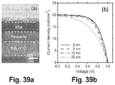
- Figure 2 also illustrates that the solar cell 200 may include a top contact constructed from a layer of molybdenum oxide 220 and aluminum 210. Embodiments of the present invention similar to that shown in Figure 2 have demonstrated superior results, especially regarding performance stability over time.
- a solar cell utilizing a molybdenum oxide/aluminum (i.e., MoO x /Al) top contact with a CH3NH3PbI3 absorber layer demonstrated an efficiency of about 11.4%.
- the molybdenum oxide/aluminum may replace noble/precious metals (e.g., Au or Ag) as a top contact for extracting photogenerated holes.
- the device performance of perovskite solar cells using a MoO x /Al top contact may be comparable to that of cells using the silver as the standard top contact.
- analysis of impedance spectroscopy measurements suggests that using a thin (e.g., 10-nm thick) MoO x /Al top contact does not appear to affect charge-recombination properties of perovskite solar cells.
- Figure 3 illustrates a method 300 of making perovskite halide films.
- the method may begin at 310 with preparing a solution that may include a solvent, a metal halide, and at least two alkyl ammonium halides.
- the solvent may be dimethylformamide (DMF)
- the metal halide may be lead iodide (PbI 2 )
- the two alkyl ammonium halides may be methyl ammonium iodide (MAI - CH 3 NH 3 I) and methyl ammonium chloride (MACl - CH 3 NH 3 Cl).
- the solution may be deposited or applied 320 to a suitable substrate; e.g. a titanium oxide surface on a transparent conducting oxide layer.
- the depositing 320 may be accomplished by any suitable means, for example, spin coating, dip coating, curtain coating, etc.
- at least a portion of the solvent may be removed from the solution.
- the depositing 320 may be followed by thermal treatment 330.
- Thermal treatment 330 may include heating the solution to at least one specified target temperature, resulting in the removal of any remaining solvent and at least one of the alkyl ammonium halides.
- the thermal treatment 330 may include a temperature ramp, such that the solution is heated over a specified range of temperature over a specified period of time.
- the solution may be allowed "dry" in ambient conditions, for example, at room temperature.
- a solution of DMF, lead iodide, MAI, and MACl may be heated to about 100°C where the solution is maintained at that temperature for about 30 minutes, resulting in the removal of substantially all of the DMF and substantially all of the MACl, resulting in the formation 340 of the target perovskite halide film on the substrate; methyl ammonium lead halide perovskite (CH 3 NH 3 PbI 3 ).
- the thermal treatment step 330 may remove substantially all of the solvent. However, in other cases small amounts of solvent may remain in the final target perovskite film. In addition,
- Figure 4 illustrates another example of the present invention, a method 400 that may produce a perovskite dihalide (e.g. containing two halogen elements).
- the method may begin with preparing 410 a solution containing a metal halide and two alkyl ammonium halides in a solvent (e.g. DMF), where each of these three compounds contain a different halogen.
- a solvent e.g. DMF
- the metal halide may be lead iodide
- the first alkyl ammonium halide may be methyl ammonium bromide (MABr)
- the second alkyl ammonium halide may be MACl.
- the solution preparation 410 may be applied 420 to a suitable substrate (e.g. spin coating). After applying 420, the solution may then be thermally treated 430 to form 440 the final perovskite halide film on the substrate.
- the final perovskite halide film may be methyl ammonium lead di-iodide bromide (CH 3 NH 3 PbI 2 Br).
- the methods summarized in Figures 3 and 4 may provide significantly improved final perovskite halide films, and better performing solar cells that incorporate these films.
- the solution may begin with an equimolar mixture of MAI and PbI 2 in the solvent.
- the use of the second alkyl ammonium halide, the MACl strongly affects the crystallization process during the thermal treatment step 330 leading to the formation 340 of the final CH 3 NH 3 PbI 3 film.
- the final CH 3 NH 3 PbI 3 film made by this method demonstrates enhanced absorption of light and significantly improved coverage of the CH 3 NH 3 PbI 3 film on its substrate.
- This method has been shown to provide measurable improvement relative to some of the standard one-step solution methods used to manufacture CH 3 NH 3 PbI 3 films.
- usage of MACl as the second alkyl ammonium halide has shown solar cells performance improvement from about 2% to 12% for a planar cell structure and from about 8% to 10% for a mesostructured device architecture, relative to one-step methods utilizing only one alkyl ammonium halide (MAI).
- FIG. 5 illustrates another exemplary method 500 for forming final perovskite halide films, according to some embodiments of the present invention.
- This method 500 may begin with preparing 510 a first solution containing a metal halide and an alkyl ammonium halide in a first solvent, where the metal halide and the alkyl ammonium halide contain different halogens.
- the first solution may be applied 520 to a substrate.
- the applying step 520 may be by spin coating, dip coating, curtain coating, and/or any other suitable solution technique. For the case of spin coating, the applying step 520 may remove some or substantially all of the first solvent.
- the solution may be thermally treated 530.
- the thermal treatment step 530 may include heating the solution to a final target temperature and then maintaining the solution at that target temperature for a defined period of time.
- the thermal treatment 530 may include a temperature ramp, such that the solution is heated over a specified range of temperature over a specified period of time.
- the solution may be allowed "dry" in ambient conditions, for example, at room temperature.
- the thermal treatment step 530 will cause the formation of an intermediate film that includes the metal halide and the alkyl ammonium halide. However, this intermediate film is only a transitory film. Eventually the thermal treating 530 removes substantially all of the alkyl ammonium halide and transforms 540 the intermediate film into a porous metal halide film.
- the metal halide film may be contacted 550 with a second solution.
- This second solution may include a second alkyl ammonium halide, different from the first, in a second solvent, which may be different from the first solvent.
- the contacting step 550 will transform 560 the metal halide film into the final target perovskite halide film.
- the contacting step 550 may also include thermally treating the second solution, by heating the solution above ambient and/or room temperature.
- the specific method 500 example shown begins with preparing 510 a first solution of lead iodide and MACl in DMF solvent.
- the first solution is then applied 520 to a substrate by spin-coating the solution onto a substrate (e.g. titanium dioxide on a transparent conducting oxide film).
- a substrate e.g. titanium dioxide on a transparent conducting oxide film.
- the solution is then thermally treated 530 by heating the solution to about 130°C and maintaining that temperature for about 30 minutes.
- the thermal treatment step 540 results in the temporary formation of an intermediate film of PbI 2 *MACl, which then degrades/decomposes/transforms 540 to a porous lead iodide film that is substantially free of solvent and MACl.
- the lead iodide film is then brought into contact 550 with a second solution prepared from a MAI in a second solvent, in this case isopropyl alcohol (IPA).
- IPA isopropyl alcohol
- the contacting step 550 is for 30 seconds at room temperature.
- the contacting step 550 may be for longer or shorter periods of time at temperatures above room temperature (e.g. up to 250°C).
- the second solvent should have a lower solubility for the final target perovskite film than the solubility of the first solvent for the final target perovskite film.
- IPA is one example, however, other common alcohol-containing solvents may also be used; e.g. butyl alcohol.
- the thermal treatment step 530 may remove substantially all of the first solvent. However, in other cases small amounts of the first solvent may remain in the porous metal halide film. Similarly, in some cases the contacting step 550 may remove substantially all of the second solvent. However, in other cases small amounts of the second solvent may remain in the final target perovskite film.
- the method illustrated in Figure 5 is referred to herein as a "three-step” method.
- the three-step method may be characterized by the formation of a transitory and thermally unstable stoichiometric precursor film of an PbI 2 ⁇ alkyl ammonium halide film (e.g. deposited onto a mesoporous TiO 2 substrate), which then during thermal treatment 530 transforms to a porous PbI 2 film.
- a transitory and thermally unstable stoichiometric precursor film of an PbI 2 ⁇ alkyl ammonium halide film e.g. deposited onto a mesoporous TiO 2 substrate
- thermal treatment 530 transforms to a porous PbI 2 film.
- some cases e.g., "drying" at room temperature
- the PbI 2 film is converted into CH 3 NH 3 PbI 3 by contacting the PbI 2 film with a solvent solution (e.g. IPA) of CH 3 NH 3 I.
- a solvent solution e.g. IPA
- embodiments of the three-step method shown in Figure 5 enable the formation of metal halide film, through the thermal decomposition of the metal halide ⁇ alkyl ammonium halide precursor film. This transition from a transitory intermediate film to a lead halide film enables the rapid conversion of metal halide film to the final target perovskite halide film, without any residual metal halide in the final target perovskite film, which results in improved device performance (e.g. solar cell).
- the disclosed one-step solution method includes introducing a second alkyl ammonium halide, MACl, to an equimolar mixture of a first alkyl ammonium halide, MAI, and a metal halide, lead iodide, in solution-to prepare perovskite CH 3 NH 3 PbI 3 on a substrate.
- substrates examples include mesoporous and planar TiO 2 substrates.
- Optical and structural characterizations show that the use of one or more alkyl ammonium halides adjusts the crystallization process for forming CH 3 NH 3 PbI 3 .
- the crystallization process may take in a time period ranging from a few minutes to several tens of minutes.
- Using two or more alkyl ammonium halides not only improves absorption of CH 3 NH 3 PbI 3 but also enhances the CH 3 NH 3 PbI 3 coverage on planar substrates, leading to significant improvement of device performance.
- methyl ammonium chloride (MACl) was used as a second alkyl ammonium halide and was mixed into a solvent solution containing MAI and PbI 2 ), to generate final target perovskite halide films of CH 3 NH 3 PbI 3 .
- Charge transport and recombination properties were examined by intensity-modulated photocurrent/photovoltage spectroscopies (IMPS/IMVS) and impedance spectroscopy (IS).
- Transparent conducting substrate and mesoporous TiO 2 films were fabricated. Initially, fluorine-doped transparent conducting SnO 2 -coated glass substrate was pre-patterned by etching with Zn powder and ⁇ 25 wt% HCl solution for about 2 minutes. The patterned FTO substrate was then cleaned by soaking in ⁇ 5 wt% NaOH in alcohol for ⁇ 16 hours and then rinsing it sequentially with deionized (DI) water and ethanol.
- DI deionized
- the cleaned FTO substrate was subsequently coated with a compact TiO 2 layer by spray pyrolysis using 0.2 M Ti(IV) bis(ethyl acetoacetate)-diisopropoxide in 1-butanol solution at ⁇ 450°C, followed by annealing at ⁇ 450°C for about one hour.
- the 20-nm-sized TiO 2 nanoparticles were synthesized utilizing standard methods known in the field.
- the TiO 2 paste, together with ⁇ 6 wt% of the 20-nm TiO 2 nanoparticles were mixed with terpineol and ethyl cellulose, and then screen-printed with 3- ⁇ m emulsion thickness on the patterned FTO substrates.
- the printed mesoporous TiO 2 film was annealed at ⁇ 500°C for about 0.5 hours.
- the average film thickness was determined by an Alpha-Step 500 surface profiler.
- the TiO 2 films were then soaked in ⁇ 0.04 M TiCl 4 solution at ⁇ 65°C for about 30 minutes, followed by rinsing with DI water and ethanol, and finally dried under N 2 .
- the TiCl 4 -treated TiO 2 films (for mesostructured cells) and compact TiO 2 films (for planar devices) on patterned FTO were annealed again at ⁇ 500°C for -30 minutes before the CH 3 NH 3 PbI 3 perovskite films were deposited on these substrates.
- CH 3 NH 3 I (MAI) was synthesized by reacting methylamine (33 wt% ethanol solution) and hydroiodic acid (57 wt% in water, Aldrich) with the molar ratio of 1.2:1 in an ice bath for 2 h with stirring followed by vacuum drying and cleaning with ethyl acetate.
- CH 3 NH 3 Cl (MACl) was synthesized by reacting methylamine (33 wt% ethanol solution) and 33 wt% hydrocholoride acid with the molar ratio of 1.2:1 in an ice bath for 2 h with stirring followed by vacuum drying and cleaning with acetonitrile.
- the perovskite CH 3 NH 3 PbI 3 precursor solutions were spin-coated onto (1) 650-nm-thick TiO 2 mesoporous films on FTO at 3,000 rpm for ⁇ 30 seconds for mesostructured cells, and (2) compact TiO 2 films on FTO at 2,500 rpm for ⁇ 10 seconds.
- the perovskite-coated films were then annealed on a hotplate at ⁇ 100°C for periods of time ranging from about 5 minutes to about 45 minutes.
- a hole-transport material (HTM) solution was spin-coated on the perovskite-covered TiO 2 electrodes at 4,000 rpm for -30 seconds.
- the HTM solution consisted of 0.1 M 2,2',7,7'-tetrakis-( N,N -di- p -methoxyphenyl-amine)-9,9'-spirobifluorene (spiro-MeOTAD), 0.035 M bis(trifluoromethane)sulfonimide lithium salt (Li-TFSi), and 0.12 M 4- tert -butylpyridine (tBP) in chlorobenzene/acetonitrile (10:1, v/v) solution. Finally, a 150-nm-thick Ag layer was deposited on the HTM layer by thermal evaporation. The active area of each device was about 0.15-0.28 cm 2 .
- the crystal structures of the perovskite films were measured by X-ray diffraction (XRD, Rigaku D/Max 2200 diffractometer with Cu K ⁇ radiation).
- XRD X-ray diffraction
- the absorption spectra of the mesoporous and planar perovskite films were characterized by a UV/Vis-NIR spectrophotometer (Cary-6000i).
- the photocurrent-voltage ( J-V ) characteristic of perovskite CH 3 NH 3 PbI 3 solar cells were measured with a Keithley 2400 source meter under the simulated AM 1.5G illumination (100 mW/cm 2 ; Oriel Sol3A Class AAA Solar Simulator), from open circuit to short circuit with a scan rate of 0.2 V/s. J-V hysteresis was observed when scanned from short circuit to open circuit, especially for planar devices. Charge transport and recombination properties of the mesostructured perovskite cells were measured by intensity-modulated photocurrent and photovoltage spectroscopies.
- Impedance spectroscopy was performed using a PARSTAT 2273 workstation with the frequency range of 0.1 Hz-100 kHz and the modulation amplitude of 10 mV.
- the IS spectra were analyzed using ZView 2.9c software (Scribner Associates).
- Figure 6 shows perovskite films prepared from CH 3 NH 3 PbI 3 precursors with different amounts of CH 3 NH 3 Cl (or MACl; as indicated) and annealed at about 100°C with varying duration (as indicated).
- Figure 6 shows the effect of varying annealing time (from about 1 minute to about 45 minutes) at about 100°C on the appearance of perovskite CH 3 NH 3 PbI 3 films prepared by using the perovskite precursors with different amounts of added CH 3 NH 3 Cl (MACl).
- the perovskite precursor solution contained PbI 2 , CH 3 NH 3 I (or MAI), and MACl with a molar ratio of 1:1: x , where x varied from 0 to 2.
- the thickness of the mesoporous TiO 2 film was about 650 nm.
- the perovskite film turned brown within one minute of annealing at 100°C. The absorbance of this film stayed virtually unchanged at 5 minutes and then decreases when annealed for 10 minutes ( Figure 7a ).
- the process that turned the perovskite film brown/dark brown with annealing occurred at significantly slower rates.
- 2 M MACl was used, it took more than 25 minutes for the perovskite film to turn brown.
- the annealing-time-dependent absorption spectra for these perovskite films prepared using different amounts of MACl are shown in Figures 7a-d .
- Figures 8a-c depict (a) XRD patterns of CH 3 NH 3 PbI 3 on mesoporous TiO 2 film as a function of the MACl amount in the precursors for different annealing time at about 100°C; magnified views of the XRD patterns (b) near 14 degrees for perovskite films using 0-2 M MACl with their respective optimum annealing time; and magnified views of the XRD patterns (c) for the 2 M MACl sample with different annealing times (from about 1 minute to about 45 minutes). Peaks associated with the perovskite CH 3 NH 3 PbI 3 structure are labeled. The other peaks are either from the TiO 2 /FTO substrate or from a transient intermediate structure related to MACl.
- Figure 8a compares the X-ray diffraction (XRD) patterns of CH 3 NH 3 PbI 3 on mesoporous TiO 2 film prepared from precursor solutions containing different amounts of MACl.
- XRD X-ray diffraction
- Table 1 shows the energy dispersive X-ray (EDX) analysis of the perovskite halide films prepared with the 2 M MACl solution, suggesting that a significant amount of chlorine is initially incorporated into the film with an I:Cl ratio of about 2.7:1.6.
- the amount of chloride detected in the perovskite film decreased rapidly from 1.6 to 0.1 during thermal treatment times ranging from about 1 minute to about 25 minutes. Longer annealing time ( ⁇ 45 minutes) led to a complete loss of chloride (within the EDX detection limit of 1%).
- the intermediate XRD peaks for the 2 M MACl samples with short annealing times are associated with the incorporation of MACl or its variation, which sublimes from the film with longer annealing times.
- the significant structural change for the 2 M MACl sample based on XRD measurement is consistent with the changes of its absorption spectra as a function of annealing time ( Figure 7d ). Similar to the 2 M MACl sample, no chloride was observed for other samples using zero molar or the other lower amounts of MACl with sufficient annealing times (Table 1).
- Figures 9a-h show the typical scanning electron microscopy (SEM) images of top views of the annealed perovskite films prepared from precursor solutions with different amounts of MACl.
- Figures 9a-d correspond to the perovskite films deposited on mesoporous TiO 2 films (650-nm thickness) using from 0 M to 2 M MACl, respectively. When no MACl was used, some islands of sub-micron-sized CH 3 NH 3 PbI 3 were observed on the top surface of the mesoporous TiO 2 film. These islands either disappeared or became less visible when MACl was used.
- Figures 10a-b depict the effect of MACl on the J - V curves of (a) mesostructured and (b) planar perovskite CH 3 NH 3 PbI 3 solar cells. All devices used spiro-MeOTAD as a hole conductor and silver as a top contact.
- Figure 10a shows the effect of MACl on the current density-voltage ( J-V ) characteristics of mesostructured perovskite solar cells based on 650-nm-thick TiO 2 mesoporous films.
- the cell with 0 M MACl demonstrated a short-circuit photocurrent density ( J sc ) of ⁇ 16.91 mA/cm 2 , open-circuit voltage ( V oc ) of ⁇ 0.835 V, and fill factor (FF) of ⁇ 0.583 to yield an efficiency ( ⁇ ) of ⁇ 8.23%.
- the cell efficiency increased to about 9% to 10% when using MACl (0.5 M to 2 M) to adjust the crystallization process of the perovskite halide; CH 3 NH 3 PbI 3 .
- the efficiency improvement resulted mainly from the higher J sc associated with stronger light absorption ( Figure 7 ) due to the use of the MACl.
- the device performance ( Figure 10b ) showed a similar trend with MACl compared to the mesostructured perovskite solar cells.
- the degree of performance improvement by MACl for planar devices was greater than the performance improvement for the mesostructured devices.
- the J sc increased from about 6 mA/cm 2 to about 18 mA/cm 2 when the amount of MACl was changed from 0 M to 0.5 M.
- 1 M to 2 M MACl was used, the J sc increased to > 20 mA/cm 2 .
- the V oc increased from about 0.8 V for 0 M MACl to > 1 V for 0.5 M to 2 M MACl.
- the FF increased from about 0.41 to a range of 0.57-0.61 for the same changes in MACl concentrations. As a result, the overall efficiency was improved from about 2% (0 M MACl) to ⁇ 11% (0.5 M MACl) to ⁇ 12% (1 M to 2 M MACl).
- the device parameters ( J sc , V oc , FF, and ⁇ ) for all these mesoporous and planar cells are summarized in Table 2.
- Figures 11a-b illustrate the effect of MACl on the recombination resistance ( R rec ) as a function of voltage for (a) mesostructured and (b) planar perovskite CH 3 NH 3 PbI 3 solar cells. Impedance spectroscopy was used to study the effect of using MACl on the recombination resistance ( R rec ) for mesostructured and planar perovskite CH 3 NH 3 PbI 3 solar cells.
- Figure 11a shows the R rec values as a function of voltage for mesostructured perovskite solar cells. The R rec for all mesostructured perovskite solar cells varied signifincantly with the bias voltage, following an approximately exponential decrease with voltage.
- perovskite films prepared from a solution containing only PbI 2 and MACl in the absence of MAI were evaluated. These films will be referred to herein as PbI 2 -MACl.
- Figure 13 shows the effect of thermal treatement time (at about 100°C) on the XRD patterns of the PbI 2 -MACl films prepared from the stoichiometric solution of PbI 2 and MACl with the same Pb concentration as used in the disclosed MACl-added solutions for making perovskite halides films; CH 3 NH 3 PbI 3 .
- the PbI 2 -MACl film displayed the characteristic perovskite (110) peak near 14 degrees.
- the perovskite film using MACl-added CH 3 NH 3 PbI 3 precursor exhibited different XRD patterns during the early stage of annealing ( Figures 8a-c ).
- the peak near 12.6 degrees may be attributed to the formation of PbI 2
- the peak near 15.5 degrees may be attributed to the formation of CH 3 NH 3 PbCl 3 .
- the intensities of both the 14- and 15.5-degree perovskite peaks decreased.
- the 12.6-degree PbI 2 peak increased with thermal treatment time. With thermal treatment times longer than about 50 minutes, the two perovskite peaks near 14 and 15.5 degrees disappear completely.
- CH 3 NH 3 PbI 3 films with MACl-added to the MAI and PbI 2 starting solution, are formed through a possible intermediate, MAI ⁇ PbI 2 ⁇ MACl, with an unknown crystalline structure.
- the additive MACl may act as a "sacrificial" agent to form this intermediate and then slowly decompose, volatilize, and/or sublime during the annealing process.
- Figures 16a-c provide (a) an SEM image, (b) XRD patterns, and (c) EDX analysis of the mixed halide CH 3 NH 3 PbI 3-x Cl x prepared from the starting solution containing MAI and PbCl 2 (at about a 3:1 molar ratio).
- Figure 16a shows the SEM image of the CH 3 NH 3 PbI 3-x Cl x film thermally treated at about 100°C for ⁇ 45 minutes.
- the overall film morphology was similar to the CH 3 NH 3 PbI 3 films prepared using the CH 3 NH 3 PbI 3 precursors with the addition of from about 1 M to about 2 M MACl ( Figures 9g and 9h ).
- Figure 17 illustrates recombination resistance R rec as a function of voltage for a planar perovskite solar cell based on the mixed halide CH 3 NH 3 PbI 3-x Cl x prepared from the starting solution containing MAI and PbCl 2 (3:1 molar ratio).
- the R rec values for the planar CH 3 NH 3 PbI 3 cells prepared from the CH 3 NH 3 PbI 3 precursor with 2-MACl additive are also plotted for comparison.
- the J-V curve for a planar CH 3 NH 3 PbI 3-x Cl x perovskite cell is shown in Figure 18 .
- the cell efficiency was ⁇ 11.86% with a J sc of ⁇ 20.57 mA/cm 2 , V oc of ⁇ 0.995 V, and FF of ⁇ 0.579.
- the performance of the planar CH 3 NH 3 PbI 3-x Cl x perovskite cell was similar to that of the planar CH 3 NH 3 PbI 3 cells prepared from the starting solutions containing from 1 M to 2 M amounts of MACl additives, as previously described.
- the R rec values for the planar CH 3 NH 3 PbI 3 cells prepared with 2-MACl additive are also plotted for comparison. It is apparent that these two samples follow almost identical voltage dependence of the recombination resistances.
- the present disclosure provides a one-step solution approach to prepare perovskite halide films (CH 3 NH 3 PbI3) on a mesoporous TiO 2 film or on a planar, compact TiO 2 layer on FTO.
- CH 3 NH 3 Cl or MACl
- CH 3 NH 3 Cl was added to a standard equimolar solution of CH 3 NH 3 I and PbI 2 to favorably adjust the crystallization process for the final target perovskite halide film; CH 3 NH 3 PbI 3 .
- the optimum crystallization time for forming pure CH 3 NH 3 PbI 3 with the strongest absorption varied from a few minutes to several tens of minutes.
- MACl not only led to enhanced absorption of CH 3 NH 3 PbI 3 , but also to significantly improved coverage of CH 3 NH 3 PbI 3 on a planar substrate.
- an alkyl ammonium halide such as MACl improves the performance of perovskite solar cells.
- the efficiency was enhanced from about 8% to 10%, whereas for the planar cell structure, the efficiency was improved from about 2% to 12%.
- the recombination resistance for planar cells was reduced by 1-2 orders of magnitude by using MACl.
- planar perovskite cells The significant performance improvement for planar perovskite cells is attributed primarily to the improved morphology of the perovskite films resulting from the additional use of MACl to control the crystallization process for forming the final target perovskite halide film, CH 3 NH 3 PbI 3 .
- Figures 19a-c depict typical SEM images of CH 3 NH PbI 2 Br films deposited on c-TiO 2 /FTO substrates from various precursor solutions: (a) PbI 2 +MABr; (b) PbI 2 +MABr+MACl; and (c) PbI 2 +MABr+2MACl.
- Figures 20a-c illustrate the effect of annealing time (as indicated) at 125°C on the XRD patterns of CH 3 NH 3 PbI 2 Br films deposited on c-TiO 2 /FTO substrate from various precursor solutions: (a) PbI 2 +MABr; (b) PbI 2 +MABr+MACl; and (c) PbI 2 +MABr+2MACl.
- Figure 21 illustrates photocurrent density-photovoltage (J-V) curves of perovskite solar cells prepared from different precursor compositions (i.e., PbI 2 +MABr or 0 MACI; PbI 2 +MABr+MACl or 1 MACl; and PbI 2 +MABr+2MACl or 2MACl).
- This one-step solution approach comprises introducing CH 3 NH 3 Cl (or MACI) to the standard CH 3 NH 3 PbI 2 Br precursor solution to prepare perovskite CH 3 NH 3 PbI 2 Br films. It has been found that the use of CH 3 NH 3 Cl alters the crystallization process for forming CH 3 NH 3 PbI 2 Br. The amount of CH 3 NH 3 Cl in the perovskite precursor solution strongly affects the film morphology ( Fig. 19 ), crystal structure formation ( Fig. 20 ), and device characteristics ( Fig. 21 ).
- This example illustrates a three-step sequential deposition method for preparing PbI 2 -free CH 3 NH 3 PbI 3 films.
- PbI 2 -free CH 3 NH 3 PbI 3 films Using typical, known two-step approaches, it is often difficult to completely convert PbI 2 into final target perovskite halide film, e.g.CH 3 NH 3 PbI 3 , without causing significant degradation of the perovskite film.
- the disclosed three-step sequential solution deposition approach provides a thermally unstable stoichiometric PbI 2 ⁇ CH 3 NH 3 Cl (PbI 2 ⁇ MACl) transitory, intermediate film that is first deposited on the mesoporous TiO 2 substrate, followed by thermal decomposition to form a PbI 2 film.
- the PbI 2 film can be rapidly converted into CH 3 NH 3 PbI 3 without any PbI 2 residue by using a MAI IPA solution at room temperature, which ultimately leads to improved device performance.
- Preparation of material for fabricating the disclosed structures, and for fabricating conventional devices used for purposes of comparison, used to quantify the improved performance of the disclosed structures proceeded as follows.
- MAI and MACl were synthesized by reacting methylamine (MA) with HI and HCl, respectively, followed by purification.
- a patterned fluorine-doped tin oxide (FTO) was first deposited with a blocking layer by spray pyrolysis at ⁇ 450°C using ⁇ 0.2 M Ti(IV) bis(ethyl acetoacetate)-diisopropoxide 1-butanol solution, followed by ⁇ 450°C annealing in air for one hour.
- a 500-nm-thick mesoporous TiO 2 film was then screen coated onto FTO followed by ⁇ 500°C annealing in air for 30 minutes.
- the TiO 2 film was then treated in 40 mM TiCl 4 aqueous solution at ⁇ 65°C for about 30 minutes.
- These TiCl 4 -treated TiO 2 films were then sequentially rinsed by deionized (DI) water, blown dry in air, and finally annealed at about 500°C for about 30 minutes.
- DI deionized
- Standard two-step deposition of perovskites proceeded as follows. From 0.4 M to about1.0 M PbI 2 (99.99%) DMF solution was spin coated onto a mesoporous TiO 2 film at 3000 rpm for about 20 seconds. The deposited PbI 2 film was then thermally treated at about 70°C for about 5 minutes. The PbI 2 film was cooled to room temperature and then immersed into a 10 mg MAI/mL isopropyl alcohol (IPA) solution for different times (from 2 minutes to about 60 minutes), followed by rinsing with IPA, blown dry with N 2 , and then thermally treated at 70°C for about 5 minutes.
- IPA isopropyl alcohol
- a first solution in DMF of 1.0 M equal molar ratio PbI 2 and MACl was first spin coated onto the mesoporous TiO 2 film at 3000 rpm for about 20 seconds.
- the applied solution was then thermally treated at about 130°C for about 30 minutes, resulting in the formation of a yellow PbI 2 film, which was then cooled to room temperature.
- the yellow PbI 2 film was then immersed into a 10 mg MAI/mL IPA solution for about 30 seconds, followed by rinsing with IPA, blown dry by N 2 , and then thermally treated at ⁇ 70°C for about 5 minutes.
- the perovskite-deposited electrodes were first coated with a layer of hole transport material (HTM) by spin coating at 4,000 rpm for 20 seconds using 0.1 M spiro-MeOTAD, 0.035 M bis(trifluoromethane)sulfonimide lithium salt (Li-TFSi), and 0.12 M 4-tert-butylpyridine (tBP) in chlorobenzene/acetonitrile (10:1, v/v) solution. A 150-nm-thick Ag contact layer was then deposited by thermal evaporation.
- HTM hole transport material
- the crystalline structures of the perovskite films were measured by X-ray diffraction (XRD, Bruker D8 ADVANCE with Cu K ⁇ radiation).
- XRD X-ray diffraction
- UV-vis ultraviolet-visible
- J-V photocurrent density-voltage
- the intensity of the CH 3 NH 3 PbI 3 peak increased, whereas the PbI 2 peak intensity decreased with longer MAI contact times (from 10 minutes to 60 minutes). Even with a 60 minutes of contact time, there was still a noticeable amount of PbI 2 in the film as indicated by the characteristic PbI 2 diffraction peak. However, the intensity of the PbI 2 peak was much smaller and almost negligible compared to the CH 3 NH 3 PbI 3 peak when the contact time was more than 30 minutes.
- Figures 23a-b illustrate the effect of PbI 2 concentration (from 0.4 M to 1.0 M) on the (a) XRD patterns and (b) UV-vis absorption spectra of the perovskite films deposited on mesoporous TiO 2 films after contacting the PbI 2 films with a 10 mg MAI/mL IPA solution for about 10 minutes.
- the impact of varying PbI 2 concentration on the PbI 2 -to-CH 3 NH 3 PbI 3 conversion using a typical two-step method was also analyzed.
- the concentration of the PbI 2 precursor solution was changed from 0.4 M to 1.0 M.
- FIG. 23a shows the XRD measurements of the perovskite films using different PbI 2 concentration with a -10 minute contact time during the second contacting step with the second solution.
- the intensity of the characteristic PbI 2 diffraction peak decreased significantly when the PbI 2 concentration was reduced from 1.0 M to 0.8 M.
- a lower degree of pore filing of PbI 2 may promote the conversion of PbI 2 into CH 3 NH 3 PbI 3 by facilitating the intercalation of MAI into PbI 2 ; but it may also result in lower absorbance due to less CH 3 NH 3 PbI 3 deposition.
- Figure 23b compares the effect of PbI 2 concentration on the UV-vis absorption spectra of the perovskite films. A higher PbI 2 concentration in the first solution for the first contacting step, generally led to stronger absorbance. The perovskite film based on a 0.4 M PbI 2 first solution displayed only about half the absorbance of the perovskite film based on a 1.0 M PbI 2 first solution.
- Table 4 summarizes the photovoltaic parameters (J sc , V oc , FF and ⁇ ) of the solar cells based on the CH 3 NH 3 PbI 3 films prepared using different concentrations of PbI 2 in the first solution of the two-step method, with 10 minute contact times in the second MAI solution during the second contacting step.
- the 0.8-M sample exhibited a low photocurrent density similar to the 1.0-M sample, which may be attributed to the residue PbI 2 observed by XRD.
- the 0.6 M sample without any PbI 2 residue exhibited a reasonable photocurrent density despite its lower absorption than the 1.0 M sample ( Figure 22b ).
- the second-step MAI dipping time is 10 min for all samples.
- the three-step sequential deposition method per embodiments of the present invention, was investigated.
- a first solution of PbI 2 and MACl in equimolar concentration
- MACl in equimolar concentration
- the resulting film Upon thermal treatment at ⁇ 130°C for about 1 minute, the resulting film exhibited a light brown color with an unknown XRD pattern.
- Its XRD pattern and UV-vis absorption spectra are shown in Figure 24a and 24b (Step 1), respectively.
- the absorption spectra were similar to those of CH 3 NH 3 PbI 3 ; however, their XRD patterns were very different.
- PbI 2 +MACl This unknown compound (denoted as PbI 2 +MACl) was likely a mixture of CH 3 NH 3 PbCl 3 , CH 3 NH 3 PbI 3 , and some unknown structure.
- the brown film slowly turned to a yellow color.
- the PbI 2 +MACl film was thermally decomposed to PbI 2 , as suggested by its UV-vis spectra and XRD pattern ( Figures 24a -b , Step 2). No traceable chlorine content could be found in this film by the energy dispersive X-ray (EDX) analysis.
- EDX energy dispersive X-ray
- the PbI 2 film formed from thermal treatment turned dark brown almost immediately after contacting with the second MAI-containing solution (with regular IPA). It took only about 30 seconds for the yellow PbI 2 film to convert into a dark-brown CH 3 NH 3 PbI 3 film ( Figure 24a , step 3) without any traceable PbI 2 evident from its XRD pattern ( Figure 24b , step 3).
- the perovskite halide target film, CH 3 NH 3 PbI 3 prepared from the initial 1.0 M PbI 2 ⁇ MACl precursor by the three-step method exhibited strong absorption (especially in the long-wavelength region) similar to the film prepared from the regular two-step approach using a 1.0 M PbI 2 first solution.
- Figure 25 is a graphical illustration of a J-V characteristic of a perovskite solar cell based on the CH 3 NH 3 PbI 3 film prepared from the disclosed three-step method.
- the cell efficiency was about 10.11%, with a J sc of ⁇ 18.64 mA/cm2, V oc of ⁇ 0.868 V, and FF of ⁇ 0.625. Both forward and backward J-V scans are shown in Figure 25 .
- the hysteresis was about 1%, and thus, can be considered negligible.
- the higher exposed surface of the PbI 2 film may facilitate the intercalation reaction between MAI with PbI 2 during the contacting step with the second solution, leading to a complete conversion of PbI 2 within about 30 seconds. With such a short contact time, the issue of CH 3 NH 3 PbI 3 dissolution in the IPA solution may be effectively mitigated.
- the present disclosure provides a three-step solution method to prepare CH 3 NH 3 PbI 3 perovskite halide films by using a second MAI-containing solution with regular (non-anhydrous) IPA.
- the disclosed three-step method enables the formation of a PbI 2 film through the thermal decomposition of an intermediate and transitory PbI 2 +MACl film.
- This intermediate film facilitates a rapid conversion of the subsequently formed PbI 2 film to the final target perovskite halide film, CH 3 NH 3 PbI 3 , without any detectable residual PbI 2 in the perovskite film, leading to improved device performance.
- the disclosed three-step solution method using regular IPA represents a promising alternative deposition method for preparing low-cost, high-efficiency perovskite solar cells.
- the three-step method provides a facile morphology-controllable sequential deposition of a planar CH 3 NH 3 PbI 3 film by stepping through a transitory intermediate PbI 2 ⁇ x MAI ( x : 0.1-0.3) precursor film.
- Adding a small amount of MAI to the PbI 2 first solution may lead to about a 10-fold faster complete formation of the final target perovskite halide film, CH 3 NH 3 PbI 3 , without any PbI 2 residue after the contacting step with the MAI-containing second solution, resulting in a much improved device performance with higher reproducibility, especially when using about 0.1 M to about 0.2M MAI in the second solution.
- Figure 26a shows the ultraviolet-visible (UV-vis) absorption spectra evolution of a pure PbI 2 film after dipping in a second solution of 10 mg/mL MAI isopropanol (IPA) for contact times up to about 30 minutes.
- the absorption shoulder near 750 nm for perovskite CH 3 NH 3 PbI 3 increased slowly with the MAI dipping time up to 20 min.
- the absorption spectrum increased very little after 20 minutes of contacting, which indicates that most PbI 2 had been converted to CH 3 NH 3 PbI 3 .
- the baseline of the absorption spectra also increased simultaneously with longer dipping time, reflecting the stronger light scattering effect associated with a rougher perovskite morphology.
- the typical scanning electron microscopy (SEM) images of planar PbI 2 and CH 3 NH 3 PbI 3 (20-min dipping/conversion) films are compared in Figure 26c and 26d , respectively.
- the planar PbI 2 film appeared porous with a coarse top surface, which may be caused by the shrinkage of the precursor film during the drying process.
- the resulting CH 3 NH 3 PbI 3 film was also full of tiny pinholes and its surface is covered with rough perovskite nanocrystals; this appearance is similar to that of the perovskite capping layer grown on a mesoporous substrate using two-step sequential deposition.
- the increased roughness of the CH 3 NH 3 PbI 3 film compared to the initial PbI 2 film may be attributed to space expansion during the second step of MAI intercalation reaction with PbI 2 .
- Figures 26a and 26b illustrate the deficiencies associated with planar CH 3 NH 3 PbI 3 thin films prepared from PbI 2 using the standard two-step sequential solution deposition method.
- the effect of varying MAI dipping time on the device characteristics is shown in Figure 27 and the corresponding photovoltaic parameters are listed Table 5.
- the cell efficiency increased significantly with longer contact time from 3.145% at 0.5 min to 6.105% at 2 min to 9.301% at 6 min, which was consistent with the more complete conversion of PbI 2 to CH 3 NH 3 PbI 3 .
- the modified three-step deposition process utilizes an alkyl ammonium halide in combination with the typical perovskite precursor, a mixture of PbI 2 and x alkyl ammonium halide with x varying from 0.1-0.3, during a first contacting step to deposit a resulting precursor film denoted as PbI 2 ⁇ x alkyl ammonium halide.
- the alkyl ammonium halide was methyl ammonium iodide (MAI).
- Figure 28b compares the XRD patterns of PbI 2 ⁇ x MAI ( x : 0-0.3) precursor films.
- the PbI 2 film displayed a strong characteristic XRD peak at about 12.5°.
- the intensity of PbI 2 peaks decreased significantly with the increase of the MAI amount used in the first-step precursor solution.
- the addition of x MAI into PbI 2 during the first deposition step did not result in any detectable CH 3 NH 3 PbI 3 diffraction peaks, such as the main (110) peak near 14°. This is consistent with the yellow appearance and the corresponding absorption spectra.
- the intensity of the main PbI 2 diffraction peak ( ⁇ 12.5°) decreased substantially with increased amounts of MAI in the precursor.
- FIG. 28c shows the UV-vis absorption spectra of the planar CH 3 NH 3 PbI 3 films using various PbI 2 ⁇ x MAI ( x : 0.1-0.3) precursor films. The absorption spectrum for PbI 2 is also shown for comparison. Consistent with their XRD results, all of these films exhibited the same absorption shoulder near 750 nm, which is typical for CH 3 NH 3 PbI 3 .
- x ⁇ 0.2 the introduction of MAI into PbI 2 led to the formation of a smoother PbI 2 ⁇ x MAI film with less pinholes than the pure PbI 2 film.
- the morphologies of the PbI 2 ⁇ 0.3MAI films became even coarser than pure PbI 2 films, which is consisted with the higher absorption baseline of the PbI 2 ⁇ 0.3MAI film as shown in Figure 28a .
- Figures 30e-h show the typical SEM images of the CH 3 NH 3 PbI 3 films prepared from PbI 2 ⁇ x MAI films after the second contacting/conversion step.
- the grain sizes of the CH 3 NH 3 PbI 3 films also showed a dependence on the amount of MAI used in the precursor.
- the CH 3 NH 3 PbI 3 film consisted mainly of relatively small CH 3 NH 3 PbI 3 nanocrystals with sizes less than 200 nm.
- the CH 3 NH 3 PbI 3 films were composed of many relatively large ( ⁇ 500 nm) crystals filled with ⁇ 200 nm small crystals; such film morphology is comparable to that of the vapor-phase-grown perovskite films. This result is also consistent with the absence of absorption baseline increase during the sequential deposition as shown in Figure 28d .
- the CH 3 NH 3 PbI 3 film looked similar to that prepared from the pure PbI 2 film.
- the added MAI was likely incorporated into the PbI 2 matrix and partially pre-expanded the volume of PbI 2 matrix.
- the degree of this pre-expansion may depend on the amount of MAI used during the first step deposition. This pre-expansion may decrease the final film expansion ratio with increasing amounts of MAI.
- m the expansion ratio.
- a best fit of the data yields m 2.02 ⁇ 0.07; the corresponding best-fit line is shown in Figure 31b .
- the addition of small amounts of MAI may result in several features that favor the rapid conversion reaction during the second step. These features may include the formation of amorphous PbI 2 ⁇ MAI, the pre-expansion of the PbI 2 matrix, and reduced crystallinity of PbI 2 . Moreover, using different amounts of MAI may allow the control of the pre-expansion of the PbI 2 ⁇ x MAI precursor film, which may give rise to the advantageous morphology shown in Figure 30 and may also affect the final photovoltaic performance of the perovskite solar cells based on the planar CH 3 NH 3 PbI 3 films.
- Figure 32 summarizes photocurrent density-voltage ( J-V ) curves of planar CH 3 NH 3 PbI 3 solar cells prepared using different PbI 2 ⁇ x MAI (x: 0-0.3) under simulated one-sun illumination. These PbI 2 ⁇ x MAI films were dipped in the MAI solution for 2 min to form the CH 3 NH 3 PbI 3 layers, which were adjusted to about 250 nm thick.
- the device shows a short-circuit photocurrent density ( J sc ) of 8.847 mA/cm 2 , open-circuit voltage ( V oc ) of 0.969 V, fill factor (FF) of 0.712, and overall conversion efficiency ( ⁇ ) of 6.105%.
- J sc photocurrent density
- V oc open-circuit voltage
- FF fill factor
- ⁇ overall conversion efficiency
- the cell efficiency increases significantly when 0.1-0.2 MAI along with PbI 2 is used during the first-step deposition, especially when 0.15 MAI is used.
- a typical efficiency for the 0.15 MAI based device is increased to 15.622% with the J sc of 19.888 mA/cm 2 , V oc of 1.065 and FF of 0.738.
- the performance improvement is largely determined by the increased J sc value associated with enhanced PbI 2 conversion process and less perovskite damage resulting from minimized interaction with IPA solvent.
- the V oc and FF values for the devices based on 0.1-0.2 MAI are also significantly larger than those of the cells based on the standard, pure PbI 2 .
- all device parameters are reduced with a typical J sc of 13.867 mA/cm 2 , V oc of 0.967 V and FF of 0.668, yielding an efficiency of 8.977%.
- the present disclosure provides the use of a precursor composition comprising a mixture of PbI 2 and MAI (molar ratio 1: x , where x varies from 0.1 to 0.3) to replace the pure PbI 2 used in the standard two-step sequential solution deposition of CH 3 NH 3 PbI 3 .
- the use of additive MAI during the first step deposition leads to about 10-fold faster CH 3 NH 3 PbI 3 formation without any PbI 2 residue during the second MAI intercalation step and ultimately results in a much improved device performance when 0.1-0.2 MAI is used.
- the morphology of the CH 3 NH 3 PbI 3 film depends on the relative amount of MAI used in the PbI 2 ⁇ x MAI precursor films during the first-step deposition, and generally demonstrates a smoother surface morphology when 0.1-0.2 MAI is used. Adding a small amount of MAI is found to lead to the formation of amorphous PbI 2 ⁇ MAI, the pre-expansion of the PbI 2 matrix, and reduced crystallinity of PbI 2 , all of which favor the complete conversion within a short period of time and thus minimizes the negative impact of the IPA solvent on the integrity of the CH 3 NH 3 PbI 3 film during the second dipping/conversion step of the standard two-step process.
- This new first-step precursor (PbI 2 ⁇ x MAI) is promising for facile preparation of high-quality planar CH 3 NH 3 PbI 3 films with controllable morphologies via the new two-step sequential solution deposition methods described herein, to fabricate high-performance perovskite solar cells.
- DMF dimethylformamide
- a patterned fluorine-doped tin oxide (FTO) was first deposited with a blocking layer by spray pyrolysis at 450°C using 0.2 M Ti(IV) bis(ethyl acetoacetate)-diisopropoxide 1-butanol solution, followed by 450 °C annealing in air for one hour.
- the different PbI 2 ⁇ x MAI films were prepared by spin coating different PbI 2 ⁇ x MAI precursor solutions (pre-warmed at 65°C) onto the substrate at 65°C at 6,000 rpm for 15 s. The spin coated PbI 2 ⁇ x MAI films were dried in air for about 30-60 min before dipping in the 10 mg/mL MAI solution at 55°C for different duration.
- the CH 3 NH 3 PbI 3 perovskite films were annealed on a hotplate at 150°C for about 1 min, and then washed again by spin coating IPA at 4,000 rpm for 15 s, followed by an additional annealing at 150°C for 1 min.
- a hole-transport material (HTM) solution was spin-coated on the perovskite-covered TiO 2 electrodes at 4,000 rpm for 30 s.
- the HTM solution consists of 0.065 M spiro-MeOTAD, 0.053 M bis(trifluoromethane)sulfonimide lithium salt (Li-TFSi) and 0.20 M 4- tert -butylpyridine (tBP) in chlorobenzene/acetonitrile (30:1, v/v) solution. Finally, a 150-nm-thick Ag layer was deposited on the HTM layer by thermal evaporation. A typical cell area was about 0.12 cm 2 as defined by a shadow mask.
- the crystal structures of the perovskite films were characterized by X-ray diffraction (XRD, Shimadzu XRD-6100 diffractometer with Cu K ⁇ radiation).
- XRD X-ray diffraction
- Shimadzu XRD-6100 diffractometer with Cu K ⁇ radiation The morphologies of the perovskite films were examined on a FEI Sirion 200 scanning electron microscope (SEM).
- SEM FEI Sirion 200 scanning electron microscope
- the optical absorption spectra of CH 3 NH 3 PbI 3 perovskite films were measured by a UV/Vis spectrophotometer (Cary-60).
- the photocurrent-voltage ( J-V ) characteristic and continuous power output of perovskite CH 3 NH 3 PbI 3 solar cells were measured respectively with a Keithley 2400 source meter and a potentiostat (Princeton Applied Research, VersaSTAT MC) under the simulated AM 1.5G illumination (100 mW/cm 2 ; Oriel Sol3A Class AAA Solar Simulator). Film thickness was measured by a surface profilometer (Dektak 8). Impedance spectroscopy (IS) was done using a PARSTAT 2273 workstation with the frequency range of 0.1 Hz-100 kHz and the modulation amplitude of 10 mV. The IS spectra were analyzed using ZView 2.9c software (Scribner Associates).
- (CH 3 NH 3 )PbI 3 is not stable (with color bleaching) under polar solvents or in solutions containing high iodine/iodide concentrations. Although the exact mechanism underlying this stability issue is unclear, the reported color bleaching for (CH 3 NH 3 )PbI 3 is irreversible.
- the (CH 3 NH 3 )PbI 3 film changes its color from brown to yellow when exposed to water, and cannot turn back from yellow to brown after the removal of water.
- This disclosure shows that the NH 3 gas induces a phase transformation of the perovskite (CH 3 NH 3 )PbI 3 film, leading to a rapid ( ⁇ 1 s) change of its color from brown to transparent across the entire visible spectral range.
- the (CH 3 NH 3 )PbI 3 films were deposited onto mesoporous TiO 2 nanocrystalline films on fluorine-doped tin oxide (FTO) by spin coating using a ⁇ -butyrolactone solution comprising 35 wt% of stoichiometric PbI 2 and CH 3 NH 3 I, as described in previous reports.
- FTO fluorine-doped tin oxide
- the effects of ammonia on the structural and optical properties of perovskite (CH 3 NH 3 )PbI 3 films were studied by X-ray diffraction (XRD, Rigaku D/Max 2200 diffractometer with Cu K ⁇ radiation) and ultraviolet-visible (UV-vis, Cary-6000i) absorption techniques.
- the transient photoresponse of (CH 3 NH 3 )PbI 3 associated with the introduction and removal of the NH 3 source was probed with a 660-nm illumination using a silicon detector connected to a potentiostat (PARSTAT 2273).
- Figures 35a-c show the sequence (left to right) of the color change of a (CH 3 NH 3 )PbI 3 film passing through the top opening of a bottle containing a 3% NH 3 solution.
- the perovskite film is deposited on a mesoporous TiO 2 film on FTO. The sample is held at each position for about 1-2 seconds.
- the brown (CH 3 NH 3 )PbI 3 film ( Fig. 35a ) immediately becomes nearly colorless when it is in contact with the NH 3 gas ( Fig. 35b ), and rapidly turns back to the brown color once the NH 3 source is removed ( Fig. 35c ).
- Figures 36a-b includes (a) UV-vis absorption spectra of a (CH 3 NH 3 )PbI 3 film in the absence and in the presence of NH 3 gas. (b) Photoresponse (transmitted light intensity) of a (CH 3 NH 3 )PbI 3 film at 660 nm as measured by a silicon detector in response to the introduction (on) and removal (off) of NH 3 gas.
- Figure 36a compares the UV-vis absorption spectra of the perovskite (CH 3 NH 3 )PbI 3 film in the absence and in the presence of NH 3 .
- the (CH 3 NH 3 )PbI 3 film starts to absorb around 750-800 nm and absorbs strongly below 600 nm, which agrees with our previous study.
- the absorption spectrum of the (CH 3 NH 3 )PbI 3 film across the entire visible region is essentially reduced to zero(i.e., the film becomes transparent in the visible region) when the perovskite film is exposed to the NH 3 gas.
- the perovskite (CH 3 NH 3 )PbI 3 film has a very wide response over the entire visible spectral range (i.e., the disappearance/substantial decrease of the entire absorption spectrum from 400 to 800 nm)
- the change of the absorption spectrum of the (CH 3 NH 3 )PbI 3 film at any single wavelength or wavelength range from 400 to 800 nm can be used.
- Figure 36b shows the photoresponse (transmitted light intensity) at 660 nm as measured by a silicon detector.
- the transmitted light intensity increases immediately ( ⁇ 1 s) after the introduction of NH 3 and also decreases quickly (1-2 s) after NH 3 is removed.
- other perovskite halides e.g., (CH 3 NH 3 )PbI 3-x Cl x and (CH 3 NH 3 )PbBr 3
- the characteristic XRD peaks (e.g., at 14.02°) for (CH 3 NH 3 )PbI 3 either disappear or become indistinguishable from the background signal. Interestingly, an unknown peak at about 11.6° arises after the NH 3 treatment. This characteristic peak cannot be assigned to either (CH 3 NH 3 )PbI 3 or PbI 2 . It is also noteworthy that the XRD pattern of the (CH 3 NH 3 )PbI 3 film in the presence of NH 3 cannot be matched to other possible compounds such as NH 4 PbI 3 , Pb(NH 3 ) 4 I 3 and NH 4 PbI 3 . x H 2 O.
- metal oxide perovskites e.g., Sr 2 RuO 4
- Sr 2 RuO 4 metal oxide perovskites
- PbI 2 also has a layered structure.
- the yellow PbI 2 can turn colorless by reacting with nitrogen-containing molecules (e.g., ammonia or pyridine) to form either an intercalation compound or a coordination complex; these colorless products can largely reverse back to the yellow PbI 2 once the nitrogen source is removed.
- nitrogen-containing molecules e.g., ammonia or pyridine
- (CH 3 NH 3 )PbI 3 shows essentially the same optical change as PbI 2 when NH 3 is introduced to or removed from the perovskite film, we hypothesize that NH 3 either intercalates into or forms a new coordination complex with the perovskite network and that the crystal structure of (CH 3 NH 3 )PbI 3 can also be largely restored once the NH 3 source is removed.
- perovskite solar cells are often made with two types of common device architectures, i.e., either mesostructured or planar thin-film solar cells.
- the first type is similar to the conventional solid-state dye-sensitized solar cells (DSSCs).
- a key component of this device configuration is a mesoporous metal-oxide (e.g., TiO 2 ) layer that is first coated with nanostructured perovskite absorbers and then infiltrated with a hole transport material (HTM; e.g., spiro-MeOTAD).
- HTM hole transport material
- perovskite can also be used as a hole conductor. In this situation, the standard HTM layer can be avoided.
- planar perovskite solar cells For the planar perovskite solar cells, a thin layer (a few hundred nanometers) of perovskite absorber is sandwiched between the electron- and hole-contact layers (e.g., TiO 2 and spiro-MeOTAD, respectively).
- the electron- and hole-contact layers e.g., TiO 2 and spiro-MeOTAD, respectively.
- a layer (about 80-150 nm thick) of Au or Ag is often used as the top metal contact for carrier extraction. Replacing Au or Ag with a low-cost material/structure that can also effectively extract photogenerated holes would help reduce the overall cost for producing perovskite solar cells.
- molybdenum oxide (MoO x ) coupled with Al can be used as an effective top-contact structure for extracting photogenerated holes from perovskite CH 3 NH 3 PbI 3 solar cells.
- transition metal oxides e.g., MoO x
- the precursor of CH 3 NH 3 I was synthesized and purified as previously reported.
- the pre-patterned fluorine-doped SnO 2 -coated glass substrate FTO; TEC15, Hartford, USA
- FTO fluorine-doped SnO 2 -coated glass substrate
- TiO 2 layer by spray pyrolysis using 0.2 M Ti(IV) bis(ethyl acetoacetate)-diisopropoxide in 1-butanol at 450°C.
- a mixture of PbCl 2 and CH 3 NH 3 I (1:3 molar ratio) was dissolved in dimethylformamide (DMF) to form the precursor solution, which was spin-coated onto the TiO 2 /FTO substrate at 2500 rpm for 10 s, followed by annealing at 100°C for 45 min in air.
- a spiro-MeOTAD-based HTM solution with a previously reported recipe was spin-coated on the perovskite-covered TiO 2 electrodes at 4000 rpm for 30 s.
- a thin layer (0-20 nm) of MoO x was deposited by thermal evaporation.
- a 150-nm-thick metal (Ag or Al) layer was deposited by thermal evaporation.
- the active area of each device was about 0.2-0.3 cm 2 .
- the X-ray diffraction (XRD) patterns of the perovskite films were conducted using Rigaku D/Max 2200 diffractometer with Cu K ⁇ radiation.
- the ultraviolet/visible (UV/vis) spectra were characterized by an ultraviolet/visible-near infrared (UV/vis-NIR) spectrophotometer (Cary-6000i).
- the morphology of perovskite film was examined by a field-emission scanning electron microscopy (FE-SEM, JEOL JSM-7000F).
- the photocurrent density-voltage ( J-V ) characteristic of perovskite solar cells were studied using a class AAA solar simulator (Oriel Sol3A).
- Impedance spectroscopy (IS) was done with a PARSTAT 2273 workstation with the frequency range of 0.1 Hz-100 kHz and modulation amplitude of 10 mV.
- Figure 38 displays the XRD patterns of a perovskite CH 3 NH 3 PbI 3 film deposited on a compact TiO 2 layer on the FTO-coated glass substrate.
- perovskite diffraction peaks denoted by stars
- the positions of these diffraction peaks are consistent with previous reports.
- the other XRD peaks are attributable to the TiO 2 /FTO substrate. No secondary phases (e.g., PbI 2 ) are found.
- Figure 39a shows the typical cross-sectional SEM image of the planar perovskite CH 3 NH 3 PbI 3 solar cell with the following layered structure: FTO/compact TiO 2 /perovskite absorber/spiro-MeOTAD/MoO x /metal.
- the metal layer is either Ag or Al.
- a 10-nm MoO x interlayer is deposited by thermal evaporation between the spiro-MeOTAD and metal layers.
- the average thickness of the CH 3 NH 3 PbI 3 layer is about 300 nm
- the average thickness of the HTM layer (spiro-MeOTAD) is about 280 nm.
- Table 7 Effect of the top layer (hole-contact) structure on the short-circuit photocurrent density J sc , open-circuit voltage V oc , fill factor FF, and conversion efficiency ⁇ of champion planar perovskite CH 3 NH 3 PbI 3 solar cells.
- the mean values and standard deviations of the PV parameters from 8-20 cells for each type of devices are given in parentheses.
- Fig. 40a the J-V characteristics of perovskite CH 3 NH 3 PbI 3 solar cells using different top-contact structures, including: (1) HTM/Ag, (2) HTM/MoO x /Ag, (3) HTM/MoO x /Al, (4) HTM/Al, and (5) MoO x /Ag (no HTM).
- top-contact structures (2), (3), and (5) we used a fixed 10-nm-thick MoO x layer.
- the composition of the spiro-MeOTAD-based HTM layer is given in detail in the experimental section.
- the cell efficiency is 11.42% with a J sc of 19.55 mA/cm 2 , V oc of 0.990 V, and FF of 0.590. All of these parameters are comparable to those of the cells using HTM/Ag and HTM/MoO x /Ag contact structures (Table 7). Consistent with the J-V results, the incident photon-to-current efficiency (IPCE) spectra for cells based on contact structures (1)-(3) are essentially identical ( Fig. 40b ). These results suggest that the junction between MoO x and the metal contact is not critical to hole extraction in perovskite solar cells.
- the perovskite solar cell only shows a conversion efficiency of 0.027% with a J sc of 0.92 mA/cm 2 , V oc of 0.182 V, and FF of 0.165. This could be attributed to the formation of a back diode at the HTM/Al interface, which creates an energy barrier limiting hole extraction. It was shown previously for PbS quantum dot solar cells that the back-diode effect can be significantly reduced when using higher work-function metals (e.g., Au or Ag) or can be completely removed by using a MoO x interlayer.
- work-function metals e.g., Au or Ag
- Impedance spectroscopy is used to study the impact of top-contact structure on the recombination resistance ( R rec ) for the perovskite solar cells.
- Fig. 41a shows the typical Nyquist plots of the complex impedance Z (i.e., the imaginary component Im [Z] versus the real component Re [Z] of the impedance) for a perovskite cell with three different bias voltages.
- the impedance spectra are dominated by a large semicircle at low frequencies. This feature has been attributed to charge recombination either at the interface between perovskite and contact layers or within the bulk perovskite layer.
- a larger semicircle corresponds to a larger recombination resistance R rec , which is inversely proportional to the recombination rate.
- the model used for impedance analysis has been previously discussed in detail by others. From these Nyquist plots, the recombination resistance of the perovskite cells can be determined.
- Fig. 41(b) shows the R rec values as a function of voltage for perovskite solar cells using the top-contact structures (1)-(3). The R rec for all these cell structures depends strongly on the bias voltage, following an approximately exponential decrease with voltage. Similar voltage dependence of recombination resistance for perovskite solar cells has been reported previously.
- Figure 42 shows the pictures of the perovskite solar cells after 15 hour continuous light soaking under simulated one sun illumination.
- the devices using MoOx showed essentially no color change of the illuminated areas.
- the device without MoOx layer showed significant color change from brown to yellow, suggesting the degradation of the perovskite layer under illumination.
- Figure 43 shows the dependence of solar cell efficiencies as a function of continuous light soaking under simulated one sun illumination for 15 hours. The efficiencies are normalized for easy comparison. The devices using MoOx/Al layer showed the best devices stability among the cells tested.
Landscapes
- Engineering & Computer Science (AREA)
- Chemical & Material Sciences (AREA)
- Manufacturing & Machinery (AREA)
- Materials Engineering (AREA)
- Chemical Kinetics & Catalysis (AREA)
- Electrochemistry (AREA)
- Power Engineering (AREA)
- Physics & Mathematics (AREA)
- Electromagnetism (AREA)
- Microelectronics & Electronic Packaging (AREA)
- Inorganic Chemistry (AREA)
- Photovoltaic Devices (AREA)
- Inorganic Compounds Of Heavy Metals (AREA)
- Chemical Vapour Deposition (AREA)
Applications Claiming Priority (6)
| Application Number | Priority Date | Filing Date | Title |
|---|---|---|---|
| US201462004020P | 2014-05-28 | 2014-05-28 | |
| US201462061475P | 2014-10-08 | 2014-10-08 | |
| US201562103277P | 2015-01-14 | 2015-01-14 | |
| PCT/US2015/033068 WO2015184197A2 (en) | 2014-05-28 | 2015-05-28 | Methods for producing and using perovskite materials and devices therefrom |
| EP15800233.7A EP3149765B1 (de) | 2014-05-28 | 2015-05-28 | Verfahren zur herstellung perowskit-materialien |
| EP18168162.8A EP3396729B1 (de) | 2014-05-28 | 2015-05-28 | Verfahren zur herstellung und verwendung von perowskit-materialien und vorrichtungen daraus |
Related Parent Applications (3)
| Application Number | Title | Priority Date | Filing Date |
|---|---|---|---|
| EP15800233.7A Division EP3149765B1 (de) | 2014-05-28 | 2015-05-28 | Verfahren zur herstellung perowskit-materialien |
| EP18168162.8A Division-Into EP3396729B1 (de) | 2014-05-28 | 2015-05-28 | Verfahren zur herstellung und verwendung von perowskit-materialien und vorrichtungen daraus |
| EP18168162.8A Division EP3396729B1 (de) | 2014-05-28 | 2015-05-28 | Verfahren zur herstellung und verwendung von perowskit-materialien und vorrichtungen daraus |
Publications (1)
| Publication Number | Publication Date |
|---|---|
| EP3595026A1 true EP3595026A1 (de) | 2020-01-15 |
Family
ID=54700065
Family Applications (3)
| Application Number | Title | Priority Date | Filing Date |
|---|---|---|---|
| EP18168162.8A Active EP3396729B1 (de) | 2014-05-28 | 2015-05-28 | Verfahren zur herstellung und verwendung von perowskit-materialien und vorrichtungen daraus |
| EP15800233.7A Active EP3149765B1 (de) | 2014-05-28 | 2015-05-28 | Verfahren zur herstellung perowskit-materialien |
| EP19193865.3A Withdrawn EP3595026A1 (de) | 2014-05-28 | 2015-05-28 | Verfahren zur herstellung und verwendung von perowskit-materialien und vorrichtungen daraus |
Family Applications Before (2)
| Application Number | Title | Priority Date | Filing Date |
|---|---|---|---|
| EP18168162.8A Active EP3396729B1 (de) | 2014-05-28 | 2015-05-28 | Verfahren zur herstellung und verwendung von perowskit-materialien und vorrichtungen daraus |
| EP15800233.7A Active EP3149765B1 (de) | 2014-05-28 | 2015-05-28 | Verfahren zur herstellung perowskit-materialien |
Country Status (3)
| Country | Link |
|---|---|
| US (2) | US10566143B2 (de) |
| EP (3) | EP3396729B1 (de) |
| WO (1) | WO2015184197A2 (de) |
Families Citing this family (26)
| Publication number | Priority date | Publication date | Assignee | Title |
|---|---|---|---|---|
| EP3243225A1 (de) * | 2015-01-07 | 2017-11-15 | Yissum Research Development Company of the Hebrew University of Jerusalem Ltd. | Selbstanordnung von perowskit zur herstellung von transparenten vorrichtungen |
| US9701696B2 (en) | 2015-02-27 | 2017-07-11 | Alliance For Sustainable Energy, Llc | Methods for producing single crystal mixed halide perovskites |
| EP3298630B1 (de) | 2015-05-19 | 2022-10-26 | Alliance for Sustainable Energy, LLC | Verfahren zur herstellung von organo-metallhalid-perovskitfilmen |
| US9905765B2 (en) * | 2015-08-13 | 2018-02-27 | Florida State University Research Foundation, Inc. | Polymer-perovskite films, devices, and methods |
| MA43050A (fr) * | 2015-09-29 | 2018-08-08 | Alliance Sustainable Energy | Dispositifs chromogènes de récolte d'énergie |
| US10622161B2 (en) | 2016-01-06 | 2020-04-14 | Nutech Ventures | Narrow band perovskite single crystal photodetectors with tunable spectral response |
| WO2017181082A1 (en) * | 2016-04-15 | 2017-10-19 | Alliance For Sustainable Energy, Llc | Nanocomposite coatings for perovskite solar cells and methods of making the same |
| CN105870339B (zh) * | 2016-04-18 | 2018-04-13 | 河北大学 | 一种提高纯度、减少针孔的钙钛矿薄膜的制备方法 |
| US10797640B2 (en) | 2016-06-05 | 2020-10-06 | Okinawa Institute Of Science And Technology School Corporation | System and method for automated performance assessment of perovskite optoelectronic devices |
| KR102068871B1 (ko) * | 2016-07-14 | 2020-01-21 | 주식회사 엘지화학 | 유무기 복합 태양전지 |
| US10861992B2 (en) | 2016-11-25 | 2020-12-08 | The Boeing Company | Perovskite solar cells for space |
| US20180282861A1 (en) * | 2017-03-14 | 2018-10-04 | Korea Research Institute Of Chemical Technology | Porous metal halide film, fabrication method thereof, and fabrication method of organometal halide having perovskite structure using the same |
| CN107265881B (zh) * | 2017-06-20 | 2020-01-10 | 宁波大学 | 多孔碘化亚铅层及应用该多孔碘化亚铅层的钙钛矿太阳能电池的制备方法 |
| CN107591486B (zh) * | 2017-08-18 | 2019-07-19 | 华中科技大学 | 一种有机无机杂化钙钛矿半导体材料及其制备方法 |
| WO2019157352A1 (en) | 2018-02-08 | 2019-08-15 | Alliance For Sustainable Energy, Llc | Perovskite materials and methods of making the same |
| JP6729626B2 (ja) * | 2018-04-18 | 2020-07-22 | ダイキン工業株式会社 | R32、R125、R143a、R1234yf及びR134aを含む冷媒を含有する組成物、並びに、その組成物を用いた冷凍方法、冷凍機の運転方法及び冷凍機 |
| US12014885B2 (en) * | 2018-04-24 | 2024-06-18 | Nutech Ventures, Inc. | Molecular doping enabled scalable blading of efficient hole transport layer-free perovskite solar cells |
| EP3794652A1 (de) | 2018-05-17 | 2021-03-24 | EMPA Eidgenössische Materialprüfungs- und Forschungsanstalt | Neuartige elektronische vorrichtung und verfahren zur schlitzdüsenabscheidung von schichten davon |
| US11024465B2 (en) * | 2018-09-14 | 2021-06-01 | Alliance For Sustainable Energy, Llc | Mixed three-dimensional and two-dimensional perovskites and methods of making the same |
| CN109181691A (zh) * | 2018-09-17 | 2019-01-11 | 天津大学 | 一种无机铵钙钛矿量子点材料及合成方法 |
| GB2577492B (en) * | 2018-09-24 | 2021-02-10 | Oxford Photovoltaics Ltd | Method of forming a crystalline or polycrystalline layer of an organic-inorganic metal halide perovskite |
| WO2020123940A1 (en) * | 2018-12-14 | 2020-06-18 | Alliance For Sustainable Energy, Llc | Manufacturing of perovskite films |
| WO2021131113A1 (ja) | 2019-12-24 | 2021-07-01 | パナソニックIpマネジメント株式会社 | 太陽電池 |
| CN111540834A (zh) * | 2020-04-16 | 2020-08-14 | 浙江浙能技术研究院有限公司 | 一种钙钛矿太阳电池阳极修饰方法 |
| CN111799382B (zh) * | 2020-06-30 | 2022-08-16 | 厦门大学 | 一种含甲胺分子的钙钛矿前驱体的制备方法 |
| WO2022104483A1 (en) * | 2020-11-23 | 2022-05-27 | Solaires Entreprises Inc. | 2d/3d alloyed halide perovskites: method for their preparation and use in solar cells |
Family Cites Families (34)
| Publication number | Priority date | Publication date | Assignee | Title |
|---|---|---|---|---|
| US5871579A (en) * | 1997-09-25 | 1999-02-16 | International Business Machines Corporation | Two-step dipping technique for the preparation of organic-inorganic perovskite thin films |
| US6231666B1 (en) * | 1999-07-20 | 2001-05-15 | Sandia Corporation | Process for forming epitaxial perovskite thin film layers using halide precursors |
| US6429318B1 (en) * | 2000-02-07 | 2002-08-06 | International Business Machines Corporaiton | Layered organic-inorganic perovskites having metal-deficient inorganic frameworks |
| US20040191150A1 (en) * | 2003-03-28 | 2004-09-30 | Takuya Yano | Perovskite complex oxide and method of producing the same |
| JP5615174B2 (ja) | 2007-07-23 | 2014-10-29 | ビーエーエスエフ ソシエタス・ヨーロピアBasf Se | 光起電力タンデム電池 |
| WO2009044614A1 (ja) | 2007-10-01 | 2009-04-09 | Rohm Co., Ltd. | 有機半導体装置 |
| US9496442B2 (en) | 2009-01-22 | 2016-11-15 | Omnipv | Solar modules including spectral concentrators and related manufacturing methods |
| GB0916037D0 (en) | 2009-09-11 | 2009-10-28 | Isis Innovation | Device |
| GB201004106D0 (en) | 2010-03-11 | 2010-04-28 | Isis Innovation | Device |
| WO2011123117A1 (en) | 2010-03-31 | 2011-10-06 | University Of Rochester | Photovoltaic cells with improved electrical contact |
| US8435486B2 (en) * | 2010-05-24 | 2013-05-07 | Toyota Jidosha Kabushiki Kaisha | Redox material for thermochemical water splitting, and method for producing hydrogen |
| BR112013024418A2 (pt) | 2011-03-29 | 2016-12-20 | Univ California | materiais ativos para dispositivos eletroópticos e dispositivos eletroópticos |
| AU2012262613B2 (en) | 2011-06-03 | 2015-07-09 | Rheem Australia Pty Limited | A water heater controller or system |
| GB201208793D0 (en) | 2012-05-18 | 2012-07-04 | Isis Innovation | Optoelectronic device |
| EP2850627B1 (de) | 2012-05-18 | 2016-04-06 | Isis Innovation Limited | Optoelektronische vorrichtung mit einem porösen gerüstmaterial und perowskiten |
| WO2013171520A1 (en) | 2012-05-18 | 2013-11-21 | Isis Innovation Limited | Optoelectronic device comprising perovskites |
| US20140060643A1 (en) | 2012-09-05 | 2014-03-06 | Lane W. Martin | Light Absorbing Oxide Materials for Photovoltaic and Photocatalytic Applications and Devices |
| ES2924644T3 (es) | 2012-09-18 | 2022-10-10 | Univ Oxford Innovation Ltd | Dispositivo optoelectrónico |
| KR20150135202A (ko) | 2012-12-20 | 2015-12-02 | 이슘 리서치 디벨롭먼트 컴퍼니 오브 더 히브루 유니버시티 오브 예루살렘, 엘티디. | 페로브스카이트 쇼트키 타입 태양 전지 |
| WO2014132076A1 (en) | 2013-03-01 | 2014-09-04 | Isis Innovation Limited | Semiconducting layer production process |
| ES2688700T3 (es) | 2013-05-06 | 2018-11-06 | Swansea University | Dispositivo fotovoltaico y procedimiento de fabricación con el uso de perovskitas |
| EP2804232A1 (de) | 2013-05-16 | 2014-11-19 | Abengoa Research S.L. | Hochleistungsfähige perovskitsensibilisierte mesoskopische Solarzellen |
| BR112015028097A2 (pt) | 2013-05-06 | 2017-07-25 | Abengoa Res Sl | método para produzir uma célula solar, método para produzir uma camada de perovskita orgânica-inorgânica nanocristalina, célula solar, e, camada de perovskita |
| TWI485154B (zh) * | 2013-05-09 | 2015-05-21 | Univ Nat Cheng Kung | 具鈣鈦礦結構吸光材料之有機混成太陽能電池及其製造方法 |
| GB201310854D0 (en) | 2013-06-18 | 2013-07-31 | Isis Innovation | Photoactive layer production process |
| EP2846371A1 (de) | 2013-09-10 | 2015-03-11 | Ecole Polytechnique Fédérale de Lausanne (EPFL) | Umgekehrte Solarzelle und Verfahren zur Herstellung davon |
| US9583724B2 (en) * | 2013-12-19 | 2017-02-28 | Nutech Ventures | Systems and methods for scalable perovskite device fabrication |
| US10199579B2 (en) * | 2013-12-19 | 2019-02-05 | Nutech Ventures | Self-powered GHZ solution-processed hybrid perovskite photodetectors |
| US10141117B2 (en) * | 2014-02-26 | 2018-11-27 | Commonwealth Scientific And Industrial Research Organisation | Process of forming a photoactive layer of a perovskite photoactive device |
| GB201407606D0 (en) | 2014-04-30 | 2014-06-11 | Cambridge Entpr Ltd | Electroluminescent device |
| CN103956394B (zh) | 2014-05-13 | 2016-08-24 | 国家纳米科学中心 | 一种改善钙钛矿太阳电池吸光层性能的方法 |
| US9701696B2 (en) | 2015-02-27 | 2017-07-11 | Alliance For Sustainable Energy, Llc | Methods for producing single crystal mixed halide perovskites |
| US9793056B1 (en) * | 2016-08-10 | 2017-10-17 | The United States Of America As Represented By The Secretary Of The Air Force | Method for producing high quality, ultra-thin organic-inorganic hybrid perovskite |
| US11104695B2 (en) * | 2018-02-19 | 2021-08-31 | The Florida State University Research Foundation, Inc. | Metal halide perovskites, light-emitting diodes, and methods |
-
2015
- 2015-05-28 EP EP18168162.8A patent/EP3396729B1/de active Active
- 2015-05-28 WO PCT/US2015/033068 patent/WO2015184197A2/en active Application Filing
- 2015-05-28 EP EP15800233.7A patent/EP3149765B1/de active Active
- 2015-05-28 EP EP19193865.3A patent/EP3595026A1/de not_active Withdrawn
- 2015-05-28 US US15/312,714 patent/US10566143B2/en active Active
-
2019
- 2019-12-05 US US16/704,207 patent/US11264179B2/en active Active
Non-Patent Citations (6)
| Title |
|---|
| JIANBO GAO ET AL: "n-Type Transition Metal Oxide as a Hole Extraction Layer in PbS Quantum Dot Solar Cells", NANO LETTERS, vol. 11, no. 8, 10 August 2011 (2011-08-10), US, pages 3263 - 3266, XP055642013, ISSN: 1530-6984, DOI: 10.1021/nl2015729 * |
| JULIAN BURSCHKA ET AL: "Sequential deposition as a route to high-performance perovskite-sensitized solar cells", NATURE, vol. 499, no. 7458, 10 July 2013 (2013-07-10), pages 316 - 319, XP055131813, ISSN: 0028-0836, DOI: 10.1038/nature12340 * |
| KWAN WEE TAN ET AL: "Thermally Induced Structural Evolution and Performance of Mesoporous Block Copolymer-Directed Alumina Perovskite Solar Cells", ACS NANO, vol. 8, no. 5, 27 May 2014 (2014-05-27), US, pages 4730 - 4739, XP055418225, ISSN: 1936-0851, DOI: 10.1021/nn500526t * |
| TAO CHEN ET AL: "Performance improvement of inverted polymer solar cells with different top electrodes by introducing a MoO3 buffer layer", APPLIED PHYSICS LETTERS, A I P PUBLISHING LLC, US, vol. 93, no. 19, 13 November 2008 (2008-11-13), pages 193307 - 193307, XP012112359, ISSN: 0003-6951, DOI: 10.1063/1.3026741 * |
| YINGZHUNAG MA ET AL: "A highly efficient mesoscopic solar cell based on CH 3 NH 3 PbI 3Àx Cl x fabricated via sequential solution deposition", CHEM. COMMUN, vol. 50, 19 May 2014 (2014-05-19), pages 12458 - 12461, XP055418161, Retrieved from the Internet <URL:http://pubs.rsc.org/en/content/articlepdf/2014/cc/c4cc01962h> [retrieved on 20171023] * |
| YIXIN ZHAO ET AL: "CH 3 NH 3 Cl-Assisted One-Step Solution Growth of CH 3 NH 3 PbI 3 : Structure, Charge-Carrier Dynamics, and Photovoltaic Properties of Perovskite Solar Cells", JOURNAL OF PHYSICAL CHEMISTRY C, vol. 118, no. 18, 30 April 2014 (2014-04-30), US, pages 9412 - 9418, XP055468631, ISSN: 1932-7447, DOI: 10.1021/jp502696w * |
Also Published As
| Publication number | Publication date |
|---|---|
| WO2015184197A4 (en) | 2016-04-14 |
| EP3149765A4 (de) | 2017-12-06 |
| US20200118767A1 (en) | 2020-04-16 |
| EP3396729A1 (de) | 2018-10-31 |
| US10566143B2 (en) | 2020-02-18 |
| EP3149765A2 (de) | 2017-04-05 |
| EP3149765B1 (de) | 2019-03-13 |
| EP3396729B1 (de) | 2019-10-09 |
| WO2015184197A3 (en) | 2016-03-03 |
| US20170186559A1 (en) | 2017-06-29 |
| WO2015184197A2 (en) | 2015-12-03 |
| US11264179B2 (en) | 2022-03-01 |
Similar Documents
| Publication | Publication Date | Title |
|---|---|---|
| US11264179B2 (en) | Methods for producing and using perovskite materials and devices therefrom | |
| KR101666563B1 (ko) | 페로브스카이트 태양전지 및 그의 제조 방법 | |
| US20230197869A1 (en) | Optoelectronic device | |
| KR101757198B1 (ko) | 페로브스카이트 제조용 전구체 및 그의 제조 방법, 그리고 페로브스카이트 태양전지 및 그의 제조 방법 | |
| EP3298630B1 (de) | Verfahren zur herstellung von organo-metallhalid-perovskitfilmen | |
| JP7166613B2 (ja) | 高効率大面積ペロブスカイト太陽電池及びその製造方法 | |
| EP3577696A1 (de) | Kontaktpassivierung für perowskit-optoelektronik | |
| EP3084854A1 (de) | Fotovoltaische vorrichtung mit einem metallhalogenid-perowskit und passivierungsmittel | |
| KR20160029790A (ko) | 태양 전지 및 이를 제조하기 위한 공정 | |
| CN105474421A (zh) | 高性能的钙钛矿敏化的介观太阳能电池 | |
| EP3223323A1 (de) | Hocheffiziente grossflächige perowskit-solarzellen und verfahren zu ihrer herstellung | |
| Venkatesan et al. | Moisture-driven phase transition for improved perovskite solar cells with reduced trap-state density | |
| Ratnasingham et al. | Novel scalable aerosol-assisted CVD route for perovskite solar cells | |
| Fan et al. | Constructing “hillocks”-like random-textured absorber for efficient planar perovskite solar cells | |
| Gkini et al. | ZrCl4 for energy level alignment at the perovskite/TiO2 interface | |
| KR102585159B1 (ko) | 친환경 용매를 사용한 페로브스카이트 결정상 전구체의 제조방법 및 이를 사용한 페로브스카이트 광전소자 | |
| Sánchez et al. | Tuning interfacial effects in hybrid perovskite solar cells | |
| Montoya | ANALYSIS OF HYBRID PEROVSKITE FILMS (MAPbI3) FABRICATED BY THE ONE AND TWO-STEPS METHODS | |
| Castro Chong | Hybrid lead halide perovskite solar cells: low-temperature processes and stability studies= Celdas solares de perovskita híbrida de haluro de plomo: procesos a baja temperatura y estudios de estabilidad | |
| WO2023047116A1 (en) | Perovskite production process |
Legal Events
| Date | Code | Title | Description |
|---|---|---|---|
| PUAI | Public reference made under article 153(3) epc to a published international application that has entered the european phase |
Free format text: ORIGINAL CODE: 0009012 |
|
| STAA | Information on the status of an ep patent application or granted ep patent |
Free format text: STATUS: THE APPLICATION HAS BEEN PUBLISHED |
|
| AC | Divisional application: reference to earlier application |
Ref document number: 3149765 Country of ref document: EP Kind code of ref document: P Ref document number: 3396729 Country of ref document: EP Kind code of ref document: P |
|
| AK | Designated contracting states |
Kind code of ref document: A1 Designated state(s): AL AT BE BG CH CY CZ DE DK EE ES FI FR GB GR HR HU IE IS IT LI LT LU LV MC MK MT NL NO PL PT RO RS SE SI SK SM TR |
|
| STAA | Information on the status of an ep patent application or granted ep patent |
Free format text: STATUS: REQUEST FOR EXAMINATION WAS MADE |
|
| 17P | Request for examination filed |
Effective date: 20200708 |
|
| RBV | Designated contracting states (corrected) |
Designated state(s): AL AT BE BG CH CY CZ DE DK EE ES FI FR GB GR HR HU IE IS IT LI LT LU LV MC MK MT NL NO PL PT RO RS SE SI SK SM TR |
|
| STAA | Information on the status of an ep patent application or granted ep patent |
Free format text: STATUS: EXAMINATION IS IN PROGRESS |
|
| 17Q | First examination report despatched |
Effective date: 20220104 |
|
| STAA | Information on the status of an ep patent application or granted ep patent |
Free format text: STATUS: THE APPLICATION IS DEEMED TO BE WITHDRAWN |
|
| 18D | Application deemed to be withdrawn |
Effective date: 20220517 |