EP3223323A1 - Hocheffiziente grossflächige perowskit-solarzellen und verfahren zu ihrer herstellung - Google Patents
Hocheffiziente grossflächige perowskit-solarzellen und verfahren zu ihrer herstellung Download PDFInfo
- Publication number
- EP3223323A1 EP3223323A1 EP16162412.7A EP16162412A EP3223323A1 EP 3223323 A1 EP3223323 A1 EP 3223323A1 EP 16162412 A EP16162412 A EP 16162412A EP 3223323 A1 EP3223323 A1 EP 3223323A1
- Authority
- EP
- European Patent Office
- Prior art keywords
- layer
- perovskite
- sensitizer
- organic
- optional
- Prior art date
- Legal status (The legal status is an assumption and is not a legal conclusion. Google has not performed a legal analysis and makes no representation as to the accuracy of the status listed.)
- Withdrawn
Links
- 238000000034 method Methods 0.000 title claims abstract description 80
- 230000008569 process Effects 0.000 title abstract description 20
- 239000010410 layer Substances 0.000 claims abstract description 229
- 229910044991 metal oxide Inorganic materials 0.000 claims abstract description 41
- 150000004706 metal oxides Chemical class 0.000 claims abstract description 41
- 239000007787 solid Substances 0.000 claims abstract description 28
- 229910001507 metal halide Inorganic materials 0.000 claims abstract description 26
- 150000005309 metal halides Chemical class 0.000 claims abstract description 26
- 238000000137 annealing Methods 0.000 claims abstract description 21
- 229910052751 metal Inorganic materials 0.000 claims abstract description 19
- 239000002184 metal Substances 0.000 claims abstract description 19
- 238000004519 manufacturing process Methods 0.000 claims abstract description 13
- 239000011241 protective layer Substances 0.000 claims abstract description 9
- 239000000463 material Substances 0.000 claims description 53
- GWEVSGVZZGPLCZ-UHFFFAOYSA-N Titan oxide Chemical compound O=[Ti]=O GWEVSGVZZGPLCZ-UHFFFAOYSA-N 0.000 claims description 37
- 230000005525 hole transport Effects 0.000 claims description 27
- -1 poly(3,4-ethylenedioxythiophene) Polymers 0.000 claims description 27
- 238000000151 deposition Methods 0.000 claims description 25
- 125000005842 heteroatom Chemical group 0.000 claims description 21
- 238000004528 spin coating Methods 0.000 claims description 18
- 150000001768 cations Chemical class 0.000 claims description 17
- XOLBLPGZBRYERU-UHFFFAOYSA-N tin dioxide Chemical compound O=[Sn]=O XOLBLPGZBRYERU-UHFFFAOYSA-N 0.000 claims description 17
- 125000004122 cyclic group Chemical group 0.000 claims description 15
- 239000004020 conductor Substances 0.000 claims description 13
- 229910001887 tin oxide Inorganic materials 0.000 claims description 13
- XLOMVQKBTHCTTD-UHFFFAOYSA-N Zinc monoxide Chemical compound [Zn]=O XLOMVQKBTHCTTD-UHFFFAOYSA-N 0.000 claims description 10
- 150000001450 anions Chemical class 0.000 claims description 10
- 125000004433 nitrogen atom Chemical group N* 0.000 claims description 9
- 238000005266 casting Methods 0.000 claims description 8
- 238000003618 dip coating Methods 0.000 claims description 8
- 229910052757 nitrogen Inorganic materials 0.000 claims description 8
- 238000005507 spraying Methods 0.000 claims description 8
- 229920000144 PEDOT:PSS Polymers 0.000 claims description 7
- XDXWNHPWWKGTKO-UHFFFAOYSA-N 207739-72-8 Chemical compound C1=CC(OC)=CC=C1N(C=1C=C2C3(C4=CC(=CC=C4C2=CC=1)N(C=1C=CC(OC)=CC=1)C=1C=CC(OC)=CC=1)C1=CC(=CC=C1C1=CC=C(C=C13)N(C=1C=CC(OC)=CC=1)C=1C=CC(OC)=CC=1)N(C=1C=CC(OC)=CC=1)C=1C=CC(OC)=CC=1)C1=CC=C(OC)C=C1 XDXWNHPWWKGTKO-UHFFFAOYSA-N 0.000 claims description 6
- LGDCSNDMFFFSHY-UHFFFAOYSA-N 4-butyl-n,n-diphenylaniline Polymers C1=CC(CCCC)=CC=C1N(C=1C=CC=CC=1)C1=CC=CC=C1 LGDCSNDMFFFSHY-UHFFFAOYSA-N 0.000 claims description 6
- 229920001609 Poly(3,4-ethylenedioxythiophene) Polymers 0.000 claims description 6
- 229910052738 indium Inorganic materials 0.000 claims description 6
- OKTJSMMVPCPJKN-UHFFFAOYSA-N Carbon Chemical compound [C] OKTJSMMVPCPJKN-UHFFFAOYSA-N 0.000 claims description 5
- 229910052731 fluorine Inorganic materials 0.000 claims description 5
- 229920003227 poly(N-vinyl carbazole) Polymers 0.000 claims description 5
- 239000011787 zinc oxide Substances 0.000 claims description 5
- UJOBWOGCFQCDNV-UHFFFAOYSA-N 9H-carbazole Chemical compound C1=CC=C2C3=CC=CC=C3NC2=C1 UJOBWOGCFQCDNV-UHFFFAOYSA-N 0.000 claims description 4
- 229910021389 graphene Inorganic materials 0.000 claims description 4
- ZKATWMILCYLAPD-UHFFFAOYSA-N niobium pentoxide Chemical compound O=[Nb](=O)O[Nb](=O)=O ZKATWMILCYLAPD-UHFFFAOYSA-N 0.000 claims description 4
- 150000003867 organic ammonium compounds Chemical group 0.000 claims description 4
- 229920001467 poly(styrenesulfonates) Polymers 0.000 claims description 4
- 229910004613 CdTe Inorganic materials 0.000 claims description 3
- YCKRFDGAMUMZLT-UHFFFAOYSA-N Fluorine atom Chemical compound [F] YCKRFDGAMUMZLT-UHFFFAOYSA-N 0.000 claims description 3
- 229910007470 ZnO—Al2O3 Inorganic materials 0.000 claims description 3
- 229910007674 ZnO—Ga2O3 Inorganic materials 0.000 claims description 3
- 229910052787 antimony Inorganic materials 0.000 claims description 3
- WATWJIUSRGPENY-UHFFFAOYSA-N antimony atom Chemical compound [Sb] WATWJIUSRGPENY-UHFFFAOYSA-N 0.000 claims description 3
- 239000011737 fluorine Substances 0.000 claims description 3
- APFVFJFRJDLVQX-UHFFFAOYSA-N indium atom Chemical compound [In] APFVFJFRJDLVQX-UHFFFAOYSA-N 0.000 claims description 3
- 239000002114 nanocomposite Substances 0.000 claims description 3
- 229910005540 GaP Inorganic materials 0.000 claims description 2
- 229910001218 Gallium arsenide Inorganic materials 0.000 claims description 2
- 229910002370 SrTiO3 Inorganic materials 0.000 claims description 2
- 235000010290 biphenyl Nutrition 0.000 claims description 2
- 239000004305 biphenyl Substances 0.000 claims description 2
- 125000006267 biphenyl group Chemical group 0.000 claims description 2
- 229910052980 cadmium sulfide Inorganic materials 0.000 claims description 2
- UHYPYGJEEGLRJD-UHFFFAOYSA-N cadmium(2+);selenium(2-) Chemical compound [Se-2].[Cd+2] UHYPYGJEEGLRJD-UHFFFAOYSA-N 0.000 claims description 2
- 150000001767 cationic compounds Chemical class 0.000 claims description 2
- 229910052949 galena Inorganic materials 0.000 claims description 2
- 229910001411 inorganic cation Inorganic materials 0.000 claims description 2
- JEIPFZHSYJVQDO-UHFFFAOYSA-N iron(III) oxide Inorganic materials O=[Fe]O[Fe]=O JEIPFZHSYJVQDO-UHFFFAOYSA-N 0.000 claims description 2
- DCZNSJVFOQPSRV-UHFFFAOYSA-N n,n-diphenyl-4-[4-(n-phenylanilino)phenyl]aniline Chemical compound C1=CC=CC=C1N(C=1C=CC(=CC=1)C=1C=CC(=CC=1)N(C=1C=CC=CC=1)C=1C=CC=CC=1)C1=CC=CC=C1 DCZNSJVFOQPSRV-UHFFFAOYSA-N 0.000 claims description 2
- JGOAZQAXRONCCI-SDNWHVSQSA-N n-[(e)-benzylideneamino]aniline Chemical group C=1C=CC=CC=1N\N=C\C1=CC=CC=C1 JGOAZQAXRONCCI-SDNWHVSQSA-N 0.000 claims description 2
- ZUOUZKKEUPVFJK-UHFFFAOYSA-N phenylbenzene Natural products C1=CC=CC=C1C1=CC=CC=C1 ZUOUZKKEUPVFJK-UHFFFAOYSA-N 0.000 claims description 2
- 229910052950 sphalerite Inorganic materials 0.000 claims description 2
- ODHXBMXNKOYIBV-UHFFFAOYSA-N triphenylamine Chemical compound C1=CC=CC=C1N(C=1C=CC=CC=1)C1=CC=CC=C1 ODHXBMXNKOYIBV-UHFFFAOYSA-N 0.000 claims description 2
- ZNOKGRXACCSDPY-UHFFFAOYSA-N tungsten(VI) oxide Inorganic materials O=[W](=O)=O ZNOKGRXACCSDPY-UHFFFAOYSA-N 0.000 claims description 2
- 229910052984 zinc sulfide Inorganic materials 0.000 claims description 2
- 102100021164 Vasodilator-stimulated phosphoprotein Human genes 0.000 abstract 1
- 239000013256 coordination polymer Substances 0.000 abstract 1
- 229910001502 inorganic halide Inorganic materials 0.000 abstract 1
- 108010054220 vasodilator-stimulated phosphoprotein Proteins 0.000 abstract 1
- 239000010408 film Substances 0.000 description 73
- 239000000243 solution Substances 0.000 description 26
- 229910052736 halogen Inorganic materials 0.000 description 14
- 150000002367 halogens Chemical class 0.000 description 13
- 125000000304 alkynyl group Chemical group 0.000 description 12
- 150000001875 compounds Chemical class 0.000 description 12
- 230000008021 deposition Effects 0.000 description 12
- 125000001424 substituent group Chemical group 0.000 description 12
- 125000003342 alkenyl group Chemical group 0.000 description 11
- 125000000217 alkyl group Chemical group 0.000 description 11
- 125000004435 hydrogen atom Chemical group [H]* 0.000 description 11
- 125000003118 aryl group Chemical group 0.000 description 10
- 238000005424 photoluminescence Methods 0.000 description 10
- 239000002243 precursor Substances 0.000 description 10
- IAZDPXIOMUYVGZ-UHFFFAOYSA-N Dimethylsulphoxide Chemical compound CS(C)=O IAZDPXIOMUYVGZ-UHFFFAOYSA-N 0.000 description 9
- 239000000758 substrate Substances 0.000 description 9
- 239000000049 pigment Substances 0.000 description 8
- 239000013078 crystal Substances 0.000 description 7
- 238000005259 measurement Methods 0.000 description 7
- 239000000203 mixture Substances 0.000 description 7
- 238000006243 chemical reaction Methods 0.000 description 6
- 229920001940 conductive polymer Polymers 0.000 description 6
- 239000011521 glass Substances 0.000 description 6
- 239000010931 gold Substances 0.000 description 6
- 125000001072 heteroaryl group Chemical group 0.000 description 6
- 229910052717 sulfur Inorganic materials 0.000 description 6
- 229910052737 gold Inorganic materials 0.000 description 5
- 238000005286 illumination Methods 0.000 description 5
- RQQRAHKHDFPBMC-UHFFFAOYSA-L lead(ii) iodide Chemical compound I[Pb]I RQQRAHKHDFPBMC-UHFFFAOYSA-L 0.000 description 5
- 150000002892 organic cations Chemical group 0.000 description 5
- 229920003023 plastic Polymers 0.000 description 5
- 239000004033 plastic Substances 0.000 description 5
- 239000002904 solvent Substances 0.000 description 5
- 238000009489 vacuum treatment Methods 0.000 description 5
- 238000009736 wetting Methods 0.000 description 5
- LFQSCWFLJHTTHZ-UHFFFAOYSA-N Ethanol Chemical compound CCO LFQSCWFLJHTTHZ-UHFFFAOYSA-N 0.000 description 4
- 238000002441 X-ray diffraction Methods 0.000 description 4
- 239000003570 air Substances 0.000 description 4
- 239000012080 ambient air Substances 0.000 description 4
- 230000015572 biosynthetic process Effects 0.000 description 4
- 229910052802 copper Inorganic materials 0.000 description 4
- 238000007766 curtain coating Methods 0.000 description 4
- 238000007641 inkjet printing Methods 0.000 description 4
- 229910052759 nickel Inorganic materials 0.000 description 4
- 229910052760 oxygen Inorganic materials 0.000 description 4
- 238000001878 scanning electron micrograph Methods 0.000 description 4
- 239000010409 thin film Substances 0.000 description 4
- YEJRWHAVMIAJKC-UHFFFAOYSA-N 4-Butyrolactone Chemical compound O=C1CCCO1 YEJRWHAVMIAJKC-UHFFFAOYSA-N 0.000 description 3
- WEVYAHXRMPXWCK-UHFFFAOYSA-N Acetonitrile Chemical compound CC#N WEVYAHXRMPXWCK-UHFFFAOYSA-N 0.000 description 3
- BAVYZALUXZFZLV-UHFFFAOYSA-O Methylammonium ion Chemical compound [NH3+]C BAVYZALUXZFZLV-UHFFFAOYSA-O 0.000 description 3
- ZMXDDKWLCZADIW-UHFFFAOYSA-N N,N-Dimethylformamide Chemical compound CN(C)C=O ZMXDDKWLCZADIW-UHFFFAOYSA-N 0.000 description 3
- MCEWYIDBDVPMES-UHFFFAOYSA-N [60]pcbm Chemical compound C123C(C4=C5C6=C7C8=C9C%10=C%11C%12=C%13C%14=C%15C%16=C%17C%18=C(C=%19C=%20C%18=C%18C%16=C%13C%13=C%11C9=C9C7=C(C=%20C9=C%13%18)C(C7=%19)=C96)C6=C%11C%17=C%15C%13=C%15C%14=C%12C%12=C%10C%10=C85)=C9C7=C6C2=C%11C%13=C2C%15=C%12C%10=C4C23C1(CCCC(=O)OC)C1=CC=CC=C1 MCEWYIDBDVPMES-UHFFFAOYSA-N 0.000 description 3
- 125000001931 aliphatic group Chemical group 0.000 description 3
- 239000012296 anti-solvent Substances 0.000 description 3
- 125000004432 carbon atom Chemical group C* 0.000 description 3
- 238000012512 characterization method Methods 0.000 description 3
- 229910052801 chlorine Inorganic materials 0.000 description 3
- 230000000875 corresponding effect Effects 0.000 description 3
- 239000006185 dispersion Substances 0.000 description 3
- 238000000295 emission spectrum Methods 0.000 description 3
- 238000002474 experimental method Methods 0.000 description 3
- RAXXELZNTBOGNW-UHFFFAOYSA-N imidazole Natural products C1=CNC=N1 RAXXELZNTBOGNW-UHFFFAOYSA-N 0.000 description 3
- 229910052741 iridium Inorganic materials 0.000 description 3
- 230000005499 meniscus Effects 0.000 description 3
- 239000002121 nanofiber Substances 0.000 description 3
- 230000006911 nucleation Effects 0.000 description 3
- 238000010899 nucleation Methods 0.000 description 3
- 229910052763 palladium Inorganic materials 0.000 description 3
- 239000002245 particle Substances 0.000 description 3
- 229910052697 platinum Inorganic materials 0.000 description 3
- 229920000642 polymer Polymers 0.000 description 3
- 229910052703 rhodium Inorganic materials 0.000 description 3
- 229910052707 ruthenium Inorganic materials 0.000 description 3
- 229910052709 silver Inorganic materials 0.000 description 3
- 230000003746 surface roughness Effects 0.000 description 3
- 229910052718 tin Inorganic materials 0.000 description 3
- 229910052719 titanium Inorganic materials 0.000 description 3
- 239000010936 titanium Substances 0.000 description 3
- XMWRBQBLMFGWIX-UHFFFAOYSA-N C60 fullerene Chemical compound C12=C3C(C4=C56)=C7C8=C5C5=C9C%10=C6C6=C4C1=C1C4=C6C6=C%10C%10=C9C9=C%11C5=C8C5=C8C7=C3C3=C7C2=C1C1=C2C4=C6C4=C%10C6=C9C9=C%11C5=C5C8=C3C3=C7C1=C1C2=C4C6=C2C9=C5C3=C12 XMWRBQBLMFGWIX-UHFFFAOYSA-N 0.000 description 2
- 125000003184 C60 fullerene group Chemical group 0.000 description 2
- PNKUSGQVOMIXLU-UHFFFAOYSA-N Formamidine Chemical compound NC=N PNKUSGQVOMIXLU-UHFFFAOYSA-N 0.000 description 2
- KFZMGEQAYNKOFK-UHFFFAOYSA-N Isopropanol Chemical compound CC(C)O KFZMGEQAYNKOFK-UHFFFAOYSA-N 0.000 description 2
- 238000002835 absorbance Methods 0.000 description 2
- 239000011149 active material Substances 0.000 description 2
- HSFWRNGVRCDJHI-UHFFFAOYSA-N alpha-acetylene Natural products C#C HSFWRNGVRCDJHI-UHFFFAOYSA-N 0.000 description 2
- 125000004429 atom Chemical group 0.000 description 2
- 229910052794 bromium Inorganic materials 0.000 description 2
- 229910052792 caesium Inorganic materials 0.000 description 2
- 239000007795 chemical reaction product Substances 0.000 description 2
- MVPPADPHJFYWMZ-UHFFFAOYSA-N chlorobenzene Chemical compound ClC1=CC=CC=C1 MVPPADPHJFYWMZ-UHFFFAOYSA-N 0.000 description 2
- 239000011248 coating agent Substances 0.000 description 2
- 238000000576 coating method Methods 0.000 description 2
- 239000000084 colloidal system Substances 0.000 description 2
- DKHNGUNXLDCATP-UHFFFAOYSA-N dipyrazino[2,3-f:2',3'-h]quinoxaline-2,3,6,7,10,11-hexacarbonitrile Chemical compound C12=NC(C#N)=C(C#N)N=C2C2=NC(C#N)=C(C#N)N=C2C2=C1N=C(C#N)C(C#N)=N2 DKHNGUNXLDCATP-UHFFFAOYSA-N 0.000 description 2
- 239000003792 electrolyte Substances 0.000 description 2
- 238000005516 engineering process Methods 0.000 description 2
- 239000007789 gas Substances 0.000 description 2
- 230000009477 glass transition Effects 0.000 description 2
- PCHJSUWPFVWCPO-UHFFFAOYSA-N gold Chemical compound [Au] PCHJSUWPFVWCPO-UHFFFAOYSA-N 0.000 description 2
- 150000004820 halides Chemical class 0.000 description 2
- 229910052740 iodine Inorganic materials 0.000 description 2
- 150000008040 ionic compounds Chemical class 0.000 description 2
- 239000007788 liquid Substances 0.000 description 2
- 239000011244 liquid electrolyte Substances 0.000 description 2
- 230000033001 locomotion Effects 0.000 description 2
- 239000012046 mixed solvent Substances 0.000 description 2
- JKQOBWVOAYFWKG-UHFFFAOYSA-N molybdenum trioxide Chemical compound O=[Mo](=O)=O JKQOBWVOAYFWKG-UHFFFAOYSA-N 0.000 description 2
- 229920001197 polyacetylene Polymers 0.000 description 2
- 229920000767 polyaniline Polymers 0.000 description 2
- 229920000128 polypyrrole Polymers 0.000 description 2
- 229920000123 polythiophene Polymers 0.000 description 2
- 238000002360 preparation method Methods 0.000 description 2
- 230000005855 radiation Effects 0.000 description 2
- 230000006798 recombination Effects 0.000 description 2
- 238000005215 recombination Methods 0.000 description 2
- 238000011160 research Methods 0.000 description 2
- 150000003839 salts Chemical class 0.000 description 2
- 238000004626 scanning electron microscopy Methods 0.000 description 2
- 238000012360 testing method Methods 0.000 description 2
- UMGDCJDMYOKAJW-UHFFFAOYSA-N thiourea Chemical compound NC(N)=S UMGDCJDMYOKAJW-UHFFFAOYSA-N 0.000 description 2
- 238000001161 time-correlated single photon counting Methods 0.000 description 2
- 229910052721 tungsten Inorganic materials 0.000 description 2
- 238000002371 ultraviolet--visible spectrum Methods 0.000 description 2
- 229910052724 xenon Inorganic materials 0.000 description 2
- FHNFHKCVQCLJFQ-UHFFFAOYSA-N xenon atom Chemical compound [Xe] FHNFHKCVQCLJFQ-UHFFFAOYSA-N 0.000 description 2
- 125000000008 (C1-C10) alkyl group Chemical group 0.000 description 1
- POILWHVDKZOXJZ-ARJAWSKDSA-M (z)-4-oxopent-2-en-2-olate Chemical compound C\C([O-])=C\C(C)=O POILWHVDKZOXJZ-ARJAWSKDSA-M 0.000 description 1
- ZXMGHDIOOHOAAE-UHFFFAOYSA-N 1,1,1-trifluoro-n-(trifluoromethylsulfonyl)methanesulfonamide Chemical compound FC(F)(F)S(=O)(=O)NS(=O)(=O)C(F)(F)F ZXMGHDIOOHOAAE-UHFFFAOYSA-N 0.000 description 1
- FGYADSCZTQOAFK-UHFFFAOYSA-N 1-methylbenzimidazole Chemical compound C1=CC=C2N(C)C=NC2=C1 FGYADSCZTQOAFK-UHFFFAOYSA-N 0.000 description 1
- STTGYIUESPWXOW-UHFFFAOYSA-N 2,9-dimethyl-4,7-diphenyl-1,10-phenanthroline Chemical compound C=12C=CC3=C(C=4C=CC=CC=4)C=C(C)N=C3C2=NC(C)=CC=1C1=CC=CC=C1 STTGYIUESPWXOW-UHFFFAOYSA-N 0.000 description 1
- GEQBRULPNIVQPP-UHFFFAOYSA-N 2-[3,5-bis(1-phenylbenzimidazol-2-yl)phenyl]-1-phenylbenzimidazole Chemical compound C1=CC=CC=C1N1C2=CC=CC=C2N=C1C1=CC(C=2N(C3=CC=CC=C3N=2)C=2C=CC=CC=2)=CC(C=2N(C3=CC=CC=C3N=2)C=2C=CC=CC=2)=C1 GEQBRULPNIVQPP-UHFFFAOYSA-N 0.000 description 1
- DIOURSRLPLXSNY-UHFFFAOYSA-N 2-[3,5-bis(4-phenyl-1h-benzimidazol-2-yl)phenyl]-4-phenyl-1h-benzimidazole Chemical compound C1=CC=CC=C1C1=CC=CC2=C1NC(C=1C=C(C=C(C=1)C=1NC3=C(C=4C=CC=CC=4)C=CC=C3N=1)C=1NC3=C(C=4C=CC=CC=4)C=CC=C3N=1)=N2 DIOURSRLPLXSNY-UHFFFAOYSA-N 0.000 description 1
- UUIMDJFBHNDZOW-UHFFFAOYSA-N 2-tert-butylpyridine Chemical compound CC(C)(C)C1=CC=CC=N1 UUIMDJFBHNDZOW-UHFFFAOYSA-N 0.000 description 1
- JFPZVDQDDRHZBN-UHFFFAOYSA-N 4-nonylpyridine Chemical compound CCCCCCCCCC1=CC=NC=C1 JFPZVDQDDRHZBN-UHFFFAOYSA-N 0.000 description 1
- YSHMQTRICHYLGF-UHFFFAOYSA-N 4-tert-butylpyridine Chemical compound CC(C)(C)C1=CC=NC=C1 YSHMQTRICHYLGF-UHFFFAOYSA-N 0.000 description 1
- AZSFNTBGCTUQFX-UHFFFAOYSA-N C12=C3C(C4=C5C=6C7=C8C9=C(C%10=6)C6=C%11C=%12C%13=C%14C%11=C9C9=C8C8=C%11C%15=C%16C=%17C(C=%18C%19=C4C7=C8C%15=%18)=C4C7=C8C%15=C%18C%20=C(C=%178)C%16=C8C%11=C9C%14=C8C%20=C%13C%18=C8C9=%12)=C%19C4=C2C7=C2C%15=C8C=4C2=C1C12C3=C5C%10=C3C6=C9C=4C32C1(CCCC(=O)OC)C1=CC=CC=C1 Chemical compound C12=C3C(C4=C5C=6C7=C8C9=C(C%10=6)C6=C%11C=%12C%13=C%14C%11=C9C9=C8C8=C%11C%15=C%16C=%17C(C=%18C%19=C4C7=C8C%15=%18)=C4C7=C8C%15=C%18C%20=C(C=%178)C%16=C8C%11=C9C%14=C8C%20=C%13C%18=C8C9=%12)=C%19C4=C2C7=C2C%15=C8C=4C2=C1C12C3=C5C%10=C3C6=C9C=4C32C1(CCCC(=O)OC)C1=CC=CC=C1 AZSFNTBGCTUQFX-UHFFFAOYSA-N 0.000 description 1
- 125000000882 C2-C6 alkenyl group Chemical group 0.000 description 1
- 229910002971 CaTiO3 Inorganic materials 0.000 description 1
- VEXZGXHMUGYJMC-UHFFFAOYSA-M Chloride anion Chemical compound [Cl-] VEXZGXHMUGYJMC-UHFFFAOYSA-M 0.000 description 1
- YZCKVEUIGOORGS-OUBTZVSYSA-N Deuterium Chemical compound [2H] YZCKVEUIGOORGS-OUBTZVSYSA-N 0.000 description 1
- 241000272186 Falco columbarius Species 0.000 description 1
- 229910000530 Gallium indium arsenide Inorganic materials 0.000 description 1
- 241001124569 Lycaenidae Species 0.000 description 1
- 238000001016 Ostwald ripening Methods 0.000 description 1
- ATJFFYVFTNAWJD-UHFFFAOYSA-N Tin Chemical compound [Sn] ATJFFYVFTNAWJD-UHFFFAOYSA-N 0.000 description 1
- RTAQQCXQSZGOHL-UHFFFAOYSA-N Titanium Chemical compound [Ti] RTAQQCXQSZGOHL-UHFFFAOYSA-N 0.000 description 1
- XSQUKJJJFZCRTK-UHFFFAOYSA-N Urea Natural products NC(N)=O XSQUKJJJFZCRTK-UHFFFAOYSA-N 0.000 description 1
- HCHKCACWOHOZIP-UHFFFAOYSA-N Zinc Chemical compound [Zn] HCHKCACWOHOZIP-UHFFFAOYSA-N 0.000 description 1
- 238000000862 absorption spectrum Methods 0.000 description 1
- 239000000654 additive Substances 0.000 description 1
- 230000000996 additive effect Effects 0.000 description 1
- 230000032683 aging Effects 0.000 description 1
- 229910052782 aluminium Inorganic materials 0.000 description 1
- 150000001412 amines Chemical class 0.000 description 1
- 238000000089 atomic force micrograph Methods 0.000 description 1
- 230000000903 blocking effect Effects 0.000 description 1
- TVFDJXOCXUVLDH-UHFFFAOYSA-N caesium atom Chemical compound [Cs] TVFDJXOCXUVLDH-UHFFFAOYSA-N 0.000 description 1
- AOWKSNWVBZGMTJ-UHFFFAOYSA-N calcium titanate Chemical compound [Ca+2].[O-][Ti]([O-])=O AOWKSNWVBZGMTJ-UHFFFAOYSA-N 0.000 description 1
- 229910052799 carbon Inorganic materials 0.000 description 1
- 150000001721 carbon Chemical group 0.000 description 1
- 239000002041 carbon nanotube Substances 0.000 description 1
- 229910021393 carbon nanotube Inorganic materials 0.000 description 1
- 239000000919 ceramic Substances 0.000 description 1
- 239000002800 charge carrier Substances 0.000 description 1
- 239000003795 chemical substances by application Substances 0.000 description 1
- 238000005229 chemical vapour deposition Methods 0.000 description 1
- 229910052804 chromium Inorganic materials 0.000 description 1
- 239000002322 conducting polymer Substances 0.000 description 1
- 238000001816 cooling Methods 0.000 description 1
- 238000012937 correction Methods 0.000 description 1
- 238000002425 crystallisation Methods 0.000 description 1
- 230000008025 crystallization Effects 0.000 description 1
- 229910052805 deuterium Inorganic materials 0.000 description 1
- ZASWJUOMEGBQCQ-UHFFFAOYSA-L dibromolead Chemical compound Br[Pb]Br ZASWJUOMEGBQCQ-UHFFFAOYSA-L 0.000 description 1
- 238000009792 diffusion process Methods 0.000 description 1
- 230000008020 evaporation Effects 0.000 description 1
- 238000001704 evaporation Methods 0.000 description 1
- 239000000835 fiber Substances 0.000 description 1
- 239000011888 foil Substances 0.000 description 1
- 238000009472 formulation Methods 0.000 description 1
- 229910003472 fullerene Inorganic materials 0.000 description 1
- 125000005843 halogen group Chemical group 0.000 description 1
- 125000004051 hexyl group Chemical group [H]C([H])([H])C([H])([H])C([H])([H])C([H])([H])C([H])([H])C([H])([H])* 0.000 description 1
- 230000006872 improvement Effects 0.000 description 1
- 238000001764 infiltration Methods 0.000 description 1
- 230000008595 infiltration Effects 0.000 description 1
- 229910052500 inorganic mineral Inorganic materials 0.000 description 1
- 239000000543 intermediate Substances 0.000 description 1
- 238000011835 investigation Methods 0.000 description 1
- 229910052742 iron Inorganic materials 0.000 description 1
- MHCFAGZWMAWTNR-UHFFFAOYSA-M lithium perchlorate Chemical compound [Li+].[O-]Cl(=O)(=O)=O MHCFAGZWMAWTNR-UHFFFAOYSA-M 0.000 description 1
- 229910001486 lithium perchlorate Inorganic materials 0.000 description 1
- QSZMZKBZAYQGRS-UHFFFAOYSA-N lithium;bis(trifluoromethylsulfonyl)azanide Chemical compound [Li+].FC(F)(F)S(=O)(=O)[N-]S(=O)(=O)C(F)(F)F QSZMZKBZAYQGRS-UHFFFAOYSA-N 0.000 description 1
- 230000007774 longterm Effects 0.000 description 1
- 229910052749 magnesium Inorganic materials 0.000 description 1
- 229910052748 manganese Inorganic materials 0.000 description 1
- 150000002739 metals Chemical class 0.000 description 1
- 125000002496 methyl group Chemical group [H]C([H])([H])* 0.000 description 1
- NQMRYBIKMRVZLB-UHFFFAOYSA-N methylamine hydrochloride Chemical compound [Cl-].[NH3+]C NQMRYBIKMRVZLB-UHFFFAOYSA-N 0.000 description 1
- 239000011707 mineral Substances 0.000 description 1
- 238000012986 modification Methods 0.000 description 1
- 230000004048 modification Effects 0.000 description 1
- 229910052758 niobium Inorganic materials 0.000 description 1
- QJGQUHMNIGDVPM-UHFFFAOYSA-N nitrogen group Chemical group [N] QJGQUHMNIGDVPM-UHFFFAOYSA-N 0.000 description 1
- 125000002347 octyl group Chemical group [H]C([*])([H])C([H])([H])C([H])([H])C([H])([H])C([H])([H])C([H])([H])C([H])([H])C([H])([H])[H] 0.000 description 1
- 229910052762 osmium Inorganic materials 0.000 description 1
- 230000035515 penetration Effects 0.000 description 1
- 238000000103 photoluminescence spectrum Methods 0.000 description 1
- 238000005240 physical vapour deposition Methods 0.000 description 1
- 239000000843 powder Substances 0.000 description 1
- 238000001556 precipitation Methods 0.000 description 1
- KVIKMJYUMZPZFU-UHFFFAOYSA-N propan-2-ol;titanium Chemical compound [Ti].CC(C)O.CC(C)O KVIKMJYUMZPZFU-UHFFFAOYSA-N 0.000 description 1
- 239000013557 residual solvent Substances 0.000 description 1
- 238000013341 scale-up Methods 0.000 description 1
- 238000007789 sealing Methods 0.000 description 1
- 229910052710 silicon Inorganic materials 0.000 description 1
- 238000010129 solution processing Methods 0.000 description 1
- 238000000935 solvent evaporation Methods 0.000 description 1
- 230000003595 spectral effect Effects 0.000 description 1
- 238000001228 spectrum Methods 0.000 description 1
- 238000005118 spray pyrolysis Methods 0.000 description 1
- 239000011550 stock solution Substances 0.000 description 1
- 238000000859 sublimation Methods 0.000 description 1
- 230000008022 sublimation Effects 0.000 description 1
- 238000006467 substitution reaction Methods 0.000 description 1
- 238000003786 synthesis reaction Methods 0.000 description 1
- 238000002207 thermal evaporation Methods 0.000 description 1
- 238000002834 transmittance Methods 0.000 description 1
- 239000012780 transparent material Substances 0.000 description 1
- 239000010937 tungsten Substances 0.000 description 1
- 238000001291 vacuum drying Methods 0.000 description 1
- XLYOFNOQVPJJNP-UHFFFAOYSA-N water Substances O XLYOFNOQVPJJNP-UHFFFAOYSA-N 0.000 description 1
- 229910052725 zinc Inorganic materials 0.000 description 1
- 239000011701 zinc Substances 0.000 description 1
- 229910052726 zirconium Inorganic materials 0.000 description 1
Images


Classifications
-
- H—ELECTRICITY
- H10—SEMICONDUCTOR DEVICES; ELECTRIC SOLID-STATE DEVICES NOT OTHERWISE PROVIDED FOR
- H10K—ORGANIC ELECTRIC SOLID-STATE DEVICES
- H10K71/00—Manufacture or treatment specially adapted for the organic devices covered by this subclass
- H10K71/10—Deposition of organic active material
- H10K71/12—Deposition of organic active material using liquid deposition, e.g. spin coating
-
- H—ELECTRICITY
- H10—SEMICONDUCTOR DEVICES; ELECTRIC SOLID-STATE DEVICES NOT OTHERWISE PROVIDED FOR
- H10K—ORGANIC ELECTRIC SOLID-STATE DEVICES
- H10K30/00—Organic devices sensitive to infrared radiation, light, electromagnetic radiation of shorter wavelength or corpuscular radiation
- H10K30/80—Constructional details
- H10K30/87—Light-trapping means
-
- H—ELECTRICITY
- H10—SEMICONDUCTOR DEVICES; ELECTRIC SOLID-STATE DEVICES NOT OTHERWISE PROVIDED FOR
- H10K—ORGANIC ELECTRIC SOLID-STATE DEVICES
- H10K71/00—Manufacture or treatment specially adapted for the organic devices covered by this subclass
- H10K71/40—Thermal treatment, e.g. annealing in the presence of a solvent vapour
-
- H—ELECTRICITY
- H10—SEMICONDUCTOR DEVICES; ELECTRIC SOLID-STATE DEVICES NOT OTHERWISE PROVIDED FOR
- H10K—ORGANIC ELECTRIC SOLID-STATE DEVICES
- H10K85/00—Organic materials used in the body or electrodes of devices covered by this subclass
- H10K85/50—Organic perovskites; Hybrid organic-inorganic perovskites [HOIP], e.g. CH3NH3PbI3
-
- H—ELECTRICITY
- H10—SEMICONDUCTOR DEVICES; ELECTRIC SOLID-STATE DEVICES NOT OTHERWISE PROVIDED FOR
- H10K—ORGANIC ELECTRIC SOLID-STATE DEVICES
- H10K30/00—Organic devices sensitive to infrared radiation, light, electromagnetic radiation of shorter wavelength or corpuscular radiation
- H10K30/10—Organic devices sensitive to infrared radiation, light, electromagnetic radiation of shorter wavelength or corpuscular radiation comprising heterojunctions between organic semiconductors and inorganic semiconductors
- H10K30/15—Sensitised wide-bandgap semiconductor devices, e.g. dye-sensitised TiO2
- H10K30/151—Sensitised wide-bandgap semiconductor devices, e.g. dye-sensitised TiO2 the wide bandgap semiconductor comprising titanium oxide, e.g. TiO2
-
- H—ELECTRICITY
- H10—SEMICONDUCTOR DEVICES; ELECTRIC SOLID-STATE DEVICES NOT OTHERWISE PROVIDED FOR
- H10K—ORGANIC ELECTRIC SOLID-STATE DEVICES
- H10K30/00—Organic devices sensitive to infrared radiation, light, electromagnetic radiation of shorter wavelength or corpuscular radiation
- H10K30/10—Organic devices sensitive to infrared radiation, light, electromagnetic radiation of shorter wavelength or corpuscular radiation comprising heterojunctions between organic semiconductors and inorganic semiconductors
- H10K30/15—Sensitised wide-bandgap semiconductor devices, e.g. dye-sensitised TiO2
- H10K30/152—Sensitised wide-bandgap semiconductor devices, e.g. dye-sensitised TiO2 the wide bandgap semiconductor comprising zinc oxide, e.g. ZnO
-
- Y—GENERAL TAGGING OF NEW TECHNOLOGICAL DEVELOPMENTS; GENERAL TAGGING OF CROSS-SECTIONAL TECHNOLOGIES SPANNING OVER SEVERAL SECTIONS OF THE IPC; TECHNICAL SUBJECTS COVERED BY FORMER USPC CROSS-REFERENCE ART COLLECTIONS [XRACs] AND DIGESTS
- Y02—TECHNOLOGIES OR APPLICATIONS FOR MITIGATION OR ADAPTATION AGAINST CLIMATE CHANGE
- Y02E—REDUCTION OF GREENHOUSE GAS [GHG] EMISSIONS, RELATED TO ENERGY GENERATION, TRANSMISSION OR DISTRIBUTION
- Y02E10/00—Energy generation through renewable energy sources
- Y02E10/50—Photovoltaic [PV] energy
- Y02E10/549—Organic PV cells
Definitions
- the present invention relates to high efficiency large area perovskite solar cells, to organic-inorganic perovskite based photoelectric conversion devices having high quality organic-inorganic perovskite film of large area (>1 cm 2 ), to high quality organic-inorganic perovskite films of large area, to methods for producing the same, in particular to vacuum-flash assisted solution process for producing the same.
- PV photovoltaics
- the sandwich/monolithic-type PV devices consisting of a mesoporous photoanode with an organic/inorganic light harvester, redox electrolyte/solid-state hole conductor, and counter electrode, have gained significant interest due to the ease of fabrication, flexibility in the selection of materials and cost effective.
- organometallic halide perovskite based on tin (CsSnX 3 ) or lead (CH 3 NH 3 PbX 3 ) have been introduced in the place of traditional metal-organic complex or organic molecules as the light harvester.
- WO 2014/020499A1 discloses a solid-state solar cell comprising a conducting support layer, a surface-increasing scaffold structure, one or more organic-inorganic perovskite layers provided on the scaffold structure and a counter electrode.
- a conducting support layer a surface-increasing scaffold structure
- organic-inorganic perovskite layers provided on the scaffold structure and a counter electrode.
- remarkable conversion efficiencies were achieved in absence of organic hole transport material or a liquid electrolyte, which rendered the latter optional.
- the annealing process results in a crystalline CH 3 NH 3 PbX 3 . From experience, the morphology of the perovskite crystals formed during this kind of solution processing cannot be well controlled and is one of the reasons for the poor reproducibility of PV cell performance.
- the present invention addresses disadvantages of devices comprising liquid electrolytes, such as the problem of solvent evaporation and the penetration of water into the solar cell caused by difficulty in long-term sealing especially in temperature cyclic tests.
- the present invention addresses the problem to scale up the production of high efficiency small laboratory cell to the production of larger area perovskite solar cells keeping their high efficiency.
- the present invention addresses the problem of the lack of reliable procedure for preparing large area PSCs and keeping their efficiency for larger area.
- the present invention addresses the disadvantages of the vacuum methods for depositing the perovskite film from solution, and for removing reaction products, such as methylammonium chloride, during the thermal annealing of the film.
- the present invention addresses the disadvantages of the other methods for producing perovskite films, which are not versatile, use anti-solvents method and cannot be adaptable for preparing larger scale PSCs.
- the present invention addresses the problem of the presence of hysteresis in the J-V (current-voltage) curves in PSCs of small size.
- the present invention addresses the problems depicted above.
- the present inventors have found that, during the preparation of sensitizer film onto a substrate comprising a conductive support layer and a metal oxide layer, the application of a vacuum drying step after the deposition of the sensitizer layer and before the annealing of the sensitizer enables the inventors to fabricate solid state solar cell, comprising an organic-inorganic perovskite with aperture area larger than 1 cm 2 and with a certified PCE of 19.6%.
- the method of the invention provides a procedure for preparing larger scale PSCs by avoiding the use of anti-solvents.
- the present invention provides a method for producing a solid state solar cell, in particular for producing a solid state solar cell comprising an organic-inorganic perovskite or organic-inorganic perovskite film and/or layer treated by vacuum after its deposition onto the metal oxide layer or onto an optional layer covering the metal oxide layer and before the annealing of the sensitizer layer comprising the organic-inorganic perovskite.
- the method of the invention allows boosting perovskite nucleation by rapid solvent removal. This creates a burst of nuclei for crystallization of perovskite and avoids pinhole formation by preventing the film from de-wetting.
- the method of the invention allows to fabricate solid state solar cell of area lager than 1 cm 2 attaining a PCE comparable to today's best CdTe and CIGS thin film photovoltaics of similar size and showing virtually no hysteresis. Furthermore the reproducibility of the method of the invention is excellent.
- the invention provides a method for producing a solid state solar cell comprising the steps of:
- the invention provides a solid state solar cell comprising a conductive support layer or current collector, a metal oxide layer, a first optional layer comprising a charge transporting layer, a sensitizer layer, a second optional layer being selected from a charge transporting layer, a protective layer, or a combination of both layers and a counter electrode or metal electrode, wherein
- the present invention provides a method for producing a solid state solar cell, in particular for producing a solid state solar cell comprising an organic-inorganic perovskite film and/or layer treated by vacuum afters its deposition and before its annealing.
- the method for producing a solid state solar cell comprises the steps of:
- the method of the invention provides a sensitizer layer comprising, consisting of an organic-inorganic perovskite or a metal halide perovskite.
- Said organic-inorganic perovskite or a metal halide perovskite is provided under a film of one perovskite pigment or mixed perovskite pigments or one or more perovskite pigments with mixed cations and anions.
- Said organic-inorganic perovskite or a metal halide perovskite forms a film, which may consist of one or more layer of one or more identical of different organic-inorganic perovskite pigments or metal halide perovskite pigments.
- Said organic-inorganic perovskite or metal halide perovskite, or organic-inorganic perovskite film or metal halide perovskite film is treated after its deposition by the application of a vacuum, which may be performed in a vacuum chamber. This step allows rapidly removing the solvent.
- the organic-inorganic perovskite film or the metal halide perovskite film is then processed to be annealed.
- perovskite refers to the “perovskite structure” and not specifically to the perovskite material, CaTiO 3 .
- perovskite encompasses and preferably relates to any material that has the same type of crystal structure as calcium titanium oxide and of materials in which the bivalent cation is replaced by two separate monovalent cations.
- the perovskite structure has the general stoichiometry AMX 3 , where "A" and "M” are cations and "X" is an anion.
- the "A” and “M” cations can have a variety of charges and in the original Perovskite mineral (CaTi0 3 ), the A cation is divalent and the M cation is tetravalent.
- the perovskite formulae includes structures having three or four anions, which may be the same or different, and/or one or two organic cations, and/or metal atoms carrying two or three positive charges, in accordance with the formulae presented elsewhere in this specification.
- the at least one sensitizer layer or the sensitizer may comprise one or more layers of an organic-inorganic perovskite or a metal halide perovskite.
- the last upper layer of organic-inorganic perovskite or metal halide perovskite is coated by the second optional layer comprising a charge transport material.
- a charge transport material is a hole transport material.
- the sensitizer layer comprises an organic-inorganic perovskite or a metal halide perovskite according to any one of perovskite-structures of formulae (I), (Ia), (Ib), (Ic), (Id), (Ie), (If) and/or (Ig) below: AA'MX 4 (I) AMX 3 (Ia) AA'N 2/3 X 4 (Ib) AN 2/3 X 3 (Ic) BN 2/3 X 4 (Id) BMX 4 (Ie) AA'A 1 MX 3 (If) AA 1 MX 3 (Ig) wherein,
- AMX 3 (formula Ia) may be expressed as formula (Ia') below: AMXiXiiXiii (Ia') wherein Xi, Xii , Xiii are independently selected from Cl - , Br - , I - , NCS - , CN - , NCO - , from [I (3-m) Cl m ] - , [I (3-n) Br n ] - , [Br (3-u) Cl u ] - , m, n u being a number between 0.0 and 3.0, and from a combination of two anion selected from Cl - , Br - , I - , preferably from halide (Cl - , Br - , I - ) and A and M are as defined elsewhere in this specification.
- Xi, Xii, Xiii may thus be the same
- Xi, Xii, Xiii in formulae (Ia) and (Ic) or Xi, Xii, Xiii, Xiv in formulae (I), (Ib), (Id) or (Ie) comprise different anions X
- Xi and Xii being the same with Xiii being an anion that is different from Xi and Xii.
- a and A' are independently selected from methylammonium cation, formamidinium cations, iodo-carbamimidoyl cation or a combination of said cations.
- said organic-inorganic perovskite or metal halide perovskite layer comprises a perovskite-structure according to any one of the formulae (Ih) to (Im): APbX 3 (Ih) ASnX 3 (Ii) ABiX 4 (Ij) AA'PbX 4 (Ik) AA'SnX 4 (IIj) BPbX 4 (Il) BSnX 4 (Im) wherein A, A', B and X are as defined above in this specification.
- X is preferably selected from Cl - , Br - and I - , most preferably X is I - or a mixture of Br - and I - .
- the at least one sensitizer layer comprising organic-inorganic perovskite or metal halide perovskite may comprise a perovskite-structure according to any of the formulae (Ih) to (Im), more preferably (Ih) and/or (Ii).
- a and A' are monovalent cations selected independently from any one of the compounds of formulae (20) to (28) below: wherein, R 7 , R 8 , R 9 and R 10 is independently selected from Cl-C15 organic substituents comprising from 0 to 15 heteroatoms.
- any one, several or all hydrogens in said substituent may be replaced by halogen and said organic substituent may comprise up to fifteen (15) N, S or O heteroatoms, and wherein, in any one of the compounds (20) to (28), the two or more of substituents present (R 7 , R 8 , R 9 and R 10 , as applicable) may be covalently connected to each other to form a substituted or unsubstituted ring or ring system.
- any heteroatom is connected to at least one carbon atom.
- neighboring heteroatoms are absent and/or heteroatom-heteroatom bonds are absent in said Cl-C15 organic substituent comprising from 0 to 15 heteroatoms.
- the heteroatoms may be selected from N, S, and/or O.
- R 7 , R 8 , R 9 and R 10 are independently selected from C 1 to C15 aliphatic and C4 to C15 aromatic or heteroaromatic substituents, wherein any one, several or all hydrogens in said substituent may be replaced by halogen and wherein, in any one of the compounds (20) to (28), the two or more of the substituents present may be covalently connected to each other to form a substituted or unsubstituted ring or ring system.
- the organic-inorganic perovskite is selected from a compound of formula (I), (Ia), (If) or (Ig).
- B is a bivalent cation selected from any one of the compounds of formulae (49) and (50) below: wherein,
- the number of heteroatoms is smaller than the number of carbons.
- the number of ring heteroatoms is smaller than the number of carbon atoms.
- G is an aliphatic, aromatic or heteroaromatic linker structure having from 1 to 10 carbons.
- R 7 , R 8 , R 9 and R 10 are independently selected from C1 to C10 alkyl, C2 to C10 alkenyl, C2 to C10 alkynyl, C4 to C10 heteroaryl and C6 to C10 aryl, wherein said alkyl, alkenyl, and alkynyl, if they comprise 3 or more carbons, may be linear, branched or cyclic, wherein said heteroaryl and aryl may be substituted or unsubstituted, and wherein several or all hydrogens in R 7 , R 8 , R 9 and R 10 may be replaced by halogen.
- R 7 , R 8, R 9 and R 10 are independently selected from C1 to C8 alkyl, C2 to C8 alkenyl, C2 to C8 alkynyl, C4 to C8 heteroaryl and C6 to C8 aryl, wherein said alkyl, alkenyl, and alkynyl, if they comprise 3 or more carbons, may be linear, branched or cyclic, wherein said heteroaryl and aryl may be substituted or unsubstituted, and wherein several or all hydrogens in R 7 , R 8 , R 9 and R 10 may be replaced by halogen.
- R 7 , R 8, R 9 and R 10 are independently selected from C1 to C6 alkyl, C2 to C6 alkenyl, C2 to C6 alkynyl, C4 to C6 heteroaryl and C6 aryl, wherein said alkyl, alkenyl, and alkynyl, if they comprise 3 or more carbons, may be linear, branched or cyclic, wherein said heteroaryl and aryl may be substituted or unsubstituted, and wherein several or all hydrogens in R 7 , R 8 , R 9 and R 10 may be replaced by halogen.
- R 7 , R 8 , R 9 and R 10 are independently selected from C1 to C4 alkyl, C2 to C4 alkenyl and C2 to C4 alkynyl, wherein said alkyl, alkenyl and alkynyl, if they comprise 3 or more carbons, may be linear, branched or cyclic, and wherein several or all hydrogens in R 7 , R 8 , R 9 and R 10 may be replaced by halogen.
- R 7 , R 8 , R 9 and R 10 are independently selected from C 1 to C3, preferably C 1 to C2 alkyl, C2 to C3, preferably C2 alkenyl and C2 to C3, preferably C2 alkynyl, wherein said alkyl, alkenyl and alkynyl, if they comprise 3 or more carbons, may be linear, branched or cyclic, and wherein several or all hydrogens in R 7 , R 8 , R 9 and R 10 may be replaced by halogen.
- R 7 , R 8 , R 9 and R 10 is independently selected from C1 to C4, more preferably C1 to C3 and even more preferably C1 to C2 alkyl. Most preferably R 7 , R 8 , R 9 and R 10 are methyl. Again, said alkyl may be completely or partially halogenated.
- A, A' and B are monovalent (A, A') and bivalent (B) cations, respectively, selected from substituted and unsubstituted C5 to C6 rings comprising one, two or more nitrogen heteroatoms, wherein one (for A and A') or two (for B) of said nitrogen atoms is/are positively charged.
- Substituents of such rings may be selected from halogen and from C 1 to C4 alkyls, C2 to C4 alkenyls and C2 to C4 alkynyls as defined above, preferably from C 1 to C3 alkyls, C3 alkenyls and C3 alkynyls as defined above.
- Said ring may comprise further heteroatoms, which may be selected from O, N and S.
- Bivalent organic cations B comprising two positively charged ring N-atoms are exemplified, for example, by the compound of formula (30) above.
- Such rings may be aromatic or aliphatic.
- A, A' and B may also comprise a ring system comprising two or more rings, at least one of which being from substituted and unsubstituted C5 to C6 ring as defined as above.
- the elliptically drawn circle in the compound of formulae (30) may also represent a ring system comprising, for example, two or more rings, but preferably two rings. Also if A and/or A' comprises two rings, further ring heteroatoms may be present, which are preferably not charged, for example.
- the organic cations A, A' and B comprise one (for A, A'), two (for B) or more nitrogen atom(s) but are free of any O or S or any other heteroatom, with the exception of halogens, which may substitute one or more hydrogen atoms in cation A and/or B.
- a and A' preferably comprise one positively charged nitrogen atom.
- B preferably comprises two positively charged nitrogen atoms.
- A, A' and B may be selected from the exemplary rings or ring systems of formulae (31) and (32) (for A, A') and from (33) to (35) (for B) below: wherein R 7 and R 8 are selected from substituents as defined above, and R 14 ,R 15 , R 16 , R 17 , R 18 , R 19 , R 20 and R 21 are independently selected from H, halogen and substituents as defined above for R 7 , R 8 , R 9 and R 10 .
- R 14 , R 15 , R 16 , R 17 , R 18 , R 19 , R 20 and R 21 are selected from H and halogen, most preferably H.
- hydrogen atoms may be substituted by halogens, such as F, Cl, I, and Br, preferably F or Cl.
- halogens such as F, Cl, I, and Br, preferably F or Cl.
- a and A' are independently selected from organic cations of formula (20) and/or formula (28).
- the metal M is selected from Sn 2+ and Pb 2+ , preferably Pb 2+ .
- N is Sb 3+ .
- the three or four X are independently selected from Cl - , Br - , and I - .
- the method of the invention provides a sensitizer layer having a thickness from 10 nm to 800 nm, 15 nm to 400 nm or 100 nm to 300 nm.
- the sensitizer layer has a thickness from 20 nm to 350 nm or 60 nm to 350 nm, preferably from 250 nm to 350 nm.
- the sensitizer layer comprises or consists of organic-inorganic perovskite has a thickness as defined above, namely from 10 nm to 800 nm, 15 nm to 400 nm, 100 nm to 300 nm, from 20 nm to 350 nm or from 60 nm to 350 nm, preferably from 250 nm to 350 nm.
- the method of the invention provides the treatment of the sensitizer layer by vacuum before the annealing of the sensitizer.
- the pressure of the vacuum is in the range from 1 to 30 Pa, 10 to 20 Pa, preferably at 20 Pa.
- the application of the vacuum lasts from 1 to 20 seconds, from 1 to 10 seconds, preferably 10 seconds.
- the conductive support layer or current collector covered by the metal oxide layer, or the metal oxide layer covered by a first optional layer, if present, and further covered by the sensitizer layer comprising the organic-inorganic perovskite is placed in a vacuum chamber at the conditions defined above and then is heated for performing the annealing.
- the step of providing the current collector or the conductive support layer and/or the step of applying the metal oxide are performed by a deposition method from a solution being selected from drop casting, spin-coating, dip-coating, curtain coating, spray-coating, and inkjet printing, meniscus coating.
- the current collector or the conductive layer has a thickness being ⁇ 30 nm, ⁇ 50 nm, ⁇ 70 nm, ⁇ 90 nm, or ⁇ 110 nm, preferably ⁇ 70 nm.
- the annealing of the sensitizer layer treated by vacuum is performed at a temperature from 80°C to 140°C, preferably at 100 °C, for 5 to 70 minutes, preferably 10 to 60 minutes.
- the step of applying the sensitizer layer comprising the organic-inorganic perovskite is performed by a deposition method selected from drop casting, spin-coating, dip-coating, spray-coating and a combination of said deposition methods.
- the deposition method is spin-coating.
- the organic-inorganic perovskite precursor may be under the form of solution in a mixed solvents comprising DMSO and Dihydrofuran-2(3H)-one, and which may be applied by spin-coating.
- the method of deposition from solution encompasses drop casting, spin-coating, dip-coating, curtain coating, spray-coating, and ink-jet printing methods.
- the sensitizer being an organic-inorganic perovskite may be also applied in one-step process from any one of the methods of deposition from a solution, dispersion, a colloid, a crystal or a salt, if solution, dispersion, colloid, crystal or salt comprises said organic-inorganic perovskite. Further application methods of organic-inorganic perovskite are described in EP13166720.6 .
- the at least one sensitizer layer or the sensitizer layer is applied directly on the metal oxide layer.
- No charge transporting layer is present between the metal oxide layer and the conductive support layer.
- Charge transporting layer comprises charge transport material may be selected from hole transport material or electron transport material.
- the first optional layer covering the metal oxide layer on the conductive support layer of current collector is an optional charge transporting layer comprising an electron charge transport material.
- the electron transport material may be selected from [6,6]-phenyl-C 61 -butyric acid methyl ester (PCBM), 1,4,5,8,9,11-hexazatriphenylene-hexacarbonitrile (HAT-CN), (C 60 -I h )[5,6]fullerene (C60), (C70-D5h)[5,6]fullerene (C70), [6,6]-Phenyl C 71 butyric acid methyl ester (PC70BM), 2,9-dimethyl-4,7-diphenyl-1,10-phenanthroline (BCP), 1,3,5-tri(phenyl-2-benzimi-dazolyl)-benzene (TPBI), preferably PCBM, HAT-CN, C60, C70, PC70BM, and metal oxide.
- PCBM 1,4,5,8,9,11-hexazatriphenylene-hexacarbonitrile
- HAT-CN 1,4,5,8,9,11-hexazatriphenylene-
- the metal oxide is an oxide of a metal selected from a group of metal consisting of Ti, Sn, Cs, Fe, Zn, W, Nb, SrTi, Si, Ti, Al, Cr, Sn, Mg, Mn, Zr, Ni, and Cu.
- the charge transporting layer comprises an electron transport material has a thickness being ⁇ 10 nm, ⁇ 20 nm, ⁇ 50 nm, preferably ⁇ 10 nm.
- the second optional layer is a charge transporting layer comprising a hole transport material.
- the application or deposition of the second optional layer comprising a charge transport material being a hole transport material is performed by a deposition method from a solution selected from drop casting, spin-coating, dip-coating, curtain coating, spray-coating, and ink-jet printing, meniscus, preferably by meniscus coating.
- the solution to be applied may comprise one or more hole transport materials or two or more solutions may be mixed and applied either in a one-step process or in a two or more sequential steps process to form a film onto the sensitizer layer comprising or consisting of the organic-inorganic sensitizer.
- the invention provides solid state solar cell comprising a conductive support layer or current collector, a metal oxide layer, a first optional layer comprising a charge transporting layer, a sensitizer layer, a second optional layer being selected from a charge transporting layer, a protective layer, or a combination of both layers and a counter electrode or metal electrode, wherein
- the sensitizer layer comprises an organic-inorganic perovskite or a metal halide perovskite is applied according to any one of deposition methods selected from drop casting, spin-coating, dip-coating, spray-coating and a combination of said deposition methods. It may also be deposited by further methods as specified herein.
- the sensitizer layer may comprise one or more organic-inorganic perovskite pigments or metal halide perovskite pigments forming one or more layers. This constitutes the organic-inorganic perovskite film or metal halide perovskite film.
- the solid state solar cell of the invention comprises a second optional layer being a charge transporting layer, preferably a charge transporting layer comprising a hole transport material.
- hole transport material By “hole transport material”, “hole transporting material”, “organic hole transport material” and “inorganic hole transport material”, and the like, is meant any material or composition wherein charges are transported by electron or hole movement (electronic motion) across said material or composition.
- the “hole transport material” is thus an electrically conductive material.
- Such hole transport materials, etc. are different from electrolytes. In this latter, charges are transported by diffusion of molecules.
- Hole transport material may be preferably selected from organic and inorganic hole transport materials.
- organic hole transport materials such as the conducting polymers disclosed elsewhere in this specification.
- a liquid and non-liquid organic hole conductor are disclosed, which may be used for the purpose of the present invention.
- organic hole transport materials (“organic electrically conducting agent”) are disclosed.
- the hole transport material is selected from triphenylamine, carbazole, N,N,(diphenyl)-N',N'di-(alkylphenyl)-4,4'-biphenyldiamine, (pTPDs), diphenylhydrazone, poly [N,N'-bis(4-butylphenyl)-N,N'-bis(phenyl)benzidine] (polyTPD), polyTPD substituted by electron donor groups and/or acceptor groups, poly(9,9-dioctylfluorene-alt-N-(4-butylphenyl)-diphenylamine (TFB), 2,2',7,7'-tetrakis-N,N-di-p-methoxyphenylamine-9,9'-spirobifluorene) (spiro-OMeTAD), N,N,N',N'-tetraphenylbenzidine (TPD).
- triphenylamine carbazo
- ionic compounds may be present in organic hole transport materials, said ionic compounds being selected from TBAPF 6 , Na CF 3 SO 3 , Li CF 3 SO 3 , LiClO 4 and Li[(CF 3 SO 2 ) 2 N.
- Other compounds that may be present in organic hole transport materials are amines, 4-tertbutylpyridine, 4-nonyl-pyridine, imidazole, N-methyl benzimidazole, for example.
- Hole transport material may be also inorganic hole transport materials.
- a wide variety of inorganic hole transport materials is commercially available. Non-limiting examples of inorganic hole transport materials are Cu 2 0, CuNCS, CuI, MoO 3 , and WO 3 .
- the solid state solar cell may comprise a protective layer as being the second optional layer.
- This protective layer may be a metal oxide layer comprising a material selected from Mg-oxide, Hf-oxide, Ga-oxide, In-oxide, Nb-oxide, Ti-oxide, Ta-oxide, Y-oxide and Zr-oxide.
- This layer may have a thickness of not more than 1.5 nm, preferably not more than 1 nm.
- Said metal oxide layer is in particular "buffer layer, which reduces or prevents recombination of photo generated electrons with the perovskite material, for example.
- the conductive support layer or current collector of the comprises a material selected from indium doped tin oxide (ITO), fluorine doped tin oxide (FTO), ZnO-Ga 2 O 3 , ZnO-Al 2 O 3 , tin oxide, antimony doped tin oxide (ATO), SrGeO 3 and zinc oxide.
- ITO indium doped tin oxide
- FTO fluorine doped tin oxide
- ZnO-Ga 2 O 3 ZnO-Al 2 O 3
- tin oxide antimony doped tin oxide
- ATO antimony doped tin oxide
- SrGeO 3 zinc oxide
- the material is preferably coated on a transparent substrate, such as plastic or glass.
- the plastic or glass provides the support structure of the layer and the cited conducting material provides the conductivity.
- Such support layers are generally known as conductive glass and conductive plastic, respectively, which are thus preferred conducting support layers in accordance with the invention.
- the conductive support layer may comprise a conducting glass or a conducting plastic.
- the current collector may also be provided by a conductive metal foil, such as titanium or zinc foil, for example.
- a conductive metal foil such as titanium or zinc foil, for example.
- Non-transparent conductive materials may be used as current collectors in particular on the side of the device that is not exposed to the light to be captured by the device.
- a metal oxide layer is applied on the conductive support layer.
- the metal oxide layer comprises a metal oxide selected from Si, TiO 2 , SnO 2 , Fe 2 O 3 , ZnO,WO 3 , Nb 2 O 5 , CdS, ZnS, PbS, Bi 2 S 3 , CdSe, CdTe, SrTiO 3 , GaP, InP, GaAs, CuInS 2 , CuInSe 2 .
- the metal oxide layer may form a scaffold structure increasing the surface of the conductive support layer.
- the solid state solar cell of the invention comprises a conductive layer, which covers the second optional layer comprising a charge transport material and comprises one or more conductive material selected from poly(3,4-ethylenedioxythiophene):poly(styrenesulfonate) (PEDOT:PSS), poly(3,4-ethylenedioxythiophene):poly(styrenesulfonate):grapheme nanocomposite (PEDOT:PSS:graphene), poly(N-vinylcarbazole) (PVK) and sulfonated poly(diphenylamine) (SPDPA), preferably from PEDOT:PSS, PEDOT:PSS:graphene and PVK, more preferably from PEDOT:PSS.
- PEDOT:PSS poly(3,4-ethylenedioxythiophene):poly(styrenesulfonate)
- PVK poly(N-vinylcarbazole)
- SPDPA sulfonated poly(dip
- Conductive polymers may also be selected from polymers comprising polyaniline, polypyrrole, polythiophene, polybenzene, polyethylenedioxythiophene, polypropylenedioxy-thiophene, polyacetylene, and combinations of two or more of the aforementioned, for example.
- the conductive polymer of the invention is preferably selected from the above polymer in a watery dispersion
- the step of applying the conductive layer is performed by a deposition method from one or more solutions of one or more conductive materials, said method selected from drop casting, spin-coating, dip-coating, curtain coating, spray-coating, and ink- jet printing, preferably by spin-coating.
- the solution may comprise one or more conductive materials or two or more solutions may mixed and applied in a one-step process to form a film onto the hole collector or applied in a process comprising two or more sequential steps.
- the step of applying the conductive layer is performed by a method selected from physical vapor deposition method group and/or from chemical vapor deposition as defined herein.
- the solar cell of the invention preferably comprises a counter electrode.
- the counter electrode generally comprises a catalytically active material, suitable to provide electrons and/or fill holes towards the inside of the device.
- the counter electrode may thus comprise one or more materials selected from Pt, Au, Ni, Cu, Ag, In, Ru, Pd, Rh, Ir, Os, C, conductive polymer and a combination of two or more of the aforementioned.
- the solid state solar cell has an aperture area >0.9 cm 2 , preferably an aperture area ⁇ 1.0 cm 2 .
- the current collector may comprise a catalytically active material, suitable to provide electrons and/or fill holes towards the inside of the device.
- the current collector may comprise a metal or a conductor or may be a metal layer or a conductor layer.
- the current collector may comprise one or more materials being metals selected from Pt, Au, Ni, Cu, Ag, In, Ru, Pd, Rh, Ir, Os, C or conductors selected from carbon nanotubes, graphene and grapheme oxides, conductive polymer and a combination of two or more of the aforementioned.
- Conductive polymers may be selected from polymers comprising polyaniline, polypyrrole, polythiophene, polybenzene, polyethylenedioxythiophene, polypropylenedioxythiophene, polyacetylene, and combinations of two or more of the aforementioned.
- the current collector comprises a metal selected from Pt, Au, Ni, Cu, Ag, In, Ru, Pd, Rh, Ir, Os, preferably Au.
- the current collector may comprise a conductor being transparent material selected from indium doped tin oxide (ITO), fluorine doped tin oxide (FTO), ZnO-Ga 2 O 3 , ZnO-Al 2 O 3 , tin oxide, antimony doped tin oxide (ATO), SrGeO 3 and zinc oxide.
- ITO indium doped tin oxide
- FTO fluorine doped tin oxide
- ZnO-Ga 2 O 3 ZnO-Al 2 O 3
- tin oxide antimony doped tin oxide
- ATO antimony doped tin oxide
- SrGeO 3 zinc oxide
- the current collector is connected to the external circuit.
- a conductive support such as conductive glass or plastic may be electrically connected to the counter electrode on the second side.
- VASP vacuum-flash assisted solution process
- a 150 nm mesoporous TiO 2 was coated on the substrate by spin-coating with a speed of 5000 rpm for 10 s with a ramp of 2000 rpm s -1 , from a diluted 30 nm particle paste (Dyesol) in Ethanol, the weight ratio of TiO 2 (Dyesol paste) and Ethanol is 6:1, and then the substrates was sintered at 500°C for 20 min.
- the perovskite film was deposited by spin-coating onto the TiO 2 substrate.
- the [FAI) 0.81 (PbI 2 ) 0.85 (MAPbBr 3 ) 0.15 ] precursor solution was prepared in glovebox from a 1.35M Pb 2+ (PbI 2 and PbBr 2 ) in the mixed solvent of DMF, GBL and DMSO, the molar ratio of GBL/DMF is 1.1.:1, and the molar ratio of Pb 2+ / [(DMSO)o.9 (thiourea) 0.1 ] is 1:1.
- the spin coating procedure was done in ambient air, first 1000 rpm for 28 s with a ramp of 200 rpm s -1 , second 4000 rpm for 18 s with a ramp of 2000 rpm s -1 .
- the substrate was put into a sample chamber connecting to gas pump system. By opening the valve connecting the specimen chamber and the low pressure system maintaining at 20 Pa for 10 s, immediately followed by full infiltration of ambient air into the specimen chamber.
- the substrate was put onto a hotplate for 1 hour at 100°C.
- a hole transporting material of Spiro-OMeTAD was deposited on top by spin-coating.
- the spin coating procedure was done in an dry air flowing glovebox, first 1500 rpm for 10 s with a ramp of 200 rpm s -1 , second 4500 rpm for 30 s with a ramp of 2000 rpm s -1 .
- the Spiro-OMeTAD solutions were prepared dissolving the spiro-OMeTAD in chlorobenzene at a concentration of 65 mM, with the addition of 30 mM bis(trifluoromethanesulfonyl)imide from a stock solution in acetonitrile), 200 mM of tertbutylpyridine. Finally, 80 nm of gold was deposited by thermal evaporation using a shadow mask to pattern the electrodes.
- X-ray diffraction (XRD) spectra were recorded on an X'Pert MPD PRO (PANalytical) equipped with a ceramic tube radiation and a RTMS X'Celerator (PANalytical). The measurements were done in BRAGG-BRENTANO geometry. The samples were mounted without further modification and the automatic divergence slit (10 mm) and beam mask (10 mm) were adjusted to the dimension of the films. A step size of 0.008° was chosen for an acquisition time of 270.57 s deg -1 . A baseline correction was applied to all X-Ray powder diffractograms to compensate for the broad feature arising from the FTO glass and anatase substrate.
- XRD X-ray diffraction
- SEM Scanning electron microscope
- Absorption spectra were measured on a PerkinElmer UV-Vis spectrophotometer._The absorbance was determined from a transmittance measurement using an integrating sphere. We used the "PerkinElmer Lambda 950 nm" set-up with the integrating sphere system "60 nm InGaAs integrating sphere" of the same company. The source are deuterium and tungsten halogen lamps and the signal is detected by a gridless photomultiplier with Peltier-controlled PbS detector. The UV WinLab software allows to process the data.
- Atomic force microscope was used to measure the surface roughness of 9 spots each 10 ⁇ 10 micrometer sized and distributed over a film surface of square-inch.
- Photoluminescence (PL) time-resolved photoluminescence (TRPL) experiments PL spectra were recorded by exciting the perovskite samples deposited onto mesoporous TiO 2 at 460 nm with a standard 450 W Xenon CW lamp. The signal was recorded by a spectrofluorometer (Fluorolog, FL1065 from Horiba Jobin Yvon Technology) and analyzed by the software FluorEssence. The PL decay experiments were performed on the same samples with the same Fluorolog with a pulsed source at 406 nm (NanoLED 402-LH from Horiba, pulse width ⁇ 200 ps, 11 pJ/pulse, approx. 1 mm 2 spot size) and the signal was recorded by the Time Correlated Single Photon Counting (TCSPC) technique. The samples were excited from the perovskite side under ambient conditions.
- TCSPC Time Correlated Single Photon Counting
- Example 2 Organic-inorganic based solar cell of the invention
- VASP also allows eliminating the hysteresis in the J-V curves, a notorious problem with PSCs.
- the exemplified solid state solar cells of the invention comprise formamidinium (FA) and methylammonium (MA) mixed cation/mixed anion perovskites of the composition [FA 0.85 MA (015) PbI 0.85 Br 0.15 ].
- the method of the invention is also enabled for solid state solar cell comprising cesium (Cs) mixed perovskite [FA x Cs (1-x) PbX 3 ] formulations.
- VASP The method of the invention(VASP) is readily scalable to the industrial level. It provides a new bench mark for pushing the perovskite solar cells towards practical applications on a large scale.
- the main fabrication steps of the perovskite film by VASP method are the following:
- Figure 1 shows scanning electron microscopy images revealing drastic differences between the (FA 0.85 MA 0.15 ) 0.95 Pb(I 0.85 Br 0.15 ) perovskite films with ( Figure 1a,b ) and without ( Figure 1c,d) vacuum-flash treatment.
- the top view of a film prepared by the conventional single step solution deposition (conventional process, CP) shows that the mesoporous TiO 2 is not fully covered by the perovskite. Big pigment grains form islands surrounded by numerous pinholes apparently due to film de-wetting during the formation of perovskite.
- VASP method yields homogeneous films without pinholes, the TiO 2 being fully covered by the perovskite grains, their size being between 400 nm and 1000 nm.
- the cross-sectional SEM images confirm the stark difference in morphology difference between films subjected or not to VASP. Without VASP treatment, a large fraction of the TiO 2 remains exposed and the other part is covered. If VASP is applied the perovskite is well infiltrated into the mesoporous TiO 2 film forming a continuous TiO 2 /perovskite nano-composite, which is covered by a -400 nm thick compact capping layer.
- the size of most of the perovskite crystallites in the capping layer is commensurate with its thickness. Hence very few grain boundaries are visible across the capping layer. This should reduce radiation-less charge carrier recombination, which is likely to occur on trapping sites associated with grain boundaries.
- the SEM top view of the freshly vacuum-flash treated film holds vital clues about the formation of the perovskite from spin-coated (FA 0.85 MA 0.15 ) 0.95 Pb((I 0.85 Br 0.15 )) 2.9 precursor films.
- the image reveals the presence of particles consisting of agglomerated nanofibers.
- the nanofibers are likely intermediates between the precursor solution and the perovskite.
- the bundled fibers form a network with bright spots at their edge, which may be attributed to crystal nuclei. Abundance of crystal nuclei would help to produce a homogeneous film by preventing de-wetting.
- Figure 2 shows the XRD spectra of the (FA 0.85 MA 0.15 ) 0.95 Pb(I 0.85 Br 0.15 ) perovskite films.
- the relative intensity of the peaks at and 14.15 degree corresponding to (-111) planes 5 and 20.05 degree corresponding to (120) planes 36 for the vacuum treated and non-vacuum treated of films are 6.2 and 4.0, respectively.
- the line broadening at half maximum intensity (FWHM) for the vacuum treated film is smaller than that of the film without vacuum treatment at the same angle.
- the FWHM for the vacuum and non-vacuum treated films at 14.15 degree are 0.13 degree and 0.156 degree; and the FWHM at 28.5 degree are 0.156 degree and 0.208 degree, respectively. It indicates the mean size of perovskite crystallites of the vacuum treated film is larger than that of the film without vacuum treatment.
- Figure 4 shows UV-vis absorption and emission spectra for the perovskite films.
- the flash vacuum treated perovskite films shows higher absorbance than the reference owing to better homogeneity. Fluorescence measurement indicates also a more intense emission for the vacuum treated film.
- the time-resolved photoluminescence Figure 4b shows that the vacuum treated film has a significantly longer fluorescence lifetime than the untreated reference. A longer photoluminescence lifetime implies less non-radiative decay, which in turn increases the photo-voltage in good agreement with the photovoltaic results.
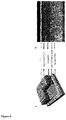
- Mesoscopic PSCs of the architecture fabricated by the method of the invention are shown in Figure 5 , and comprise perovskite thin films of the composition (FA 0.85 MA 0.15 ) 0.95 Pb(I 0.85 Br 0.15 ) as light harvesters (sensitizer).
- F-V photocurrent density vs . voltage
- IPCE incident-photon-to-current conversion efficiency
- Table 1 Photovoltaic parameters of a batch of twenty [FAI) 0.81 (PbI 2 ) 0.85 (MAPbBr 3 ) 0.15 ] based perovskite devices fabricated by conventional process (CP) measured with an aperture area of 1.00 cm 2 under standard AM 1.5G (air mass 1.5 global) illumination.
- CP conventional process
- the VASP vastly improved device performance and reproducibility compared to the CP method.
- the average PCE for twenty PSCs obtained via the CP method was 9.62 ⁇ 0.67 % with short circuit photocurrent density ( J sc ) of 17.25 ⁇ 0.49 mA cm -2 , open circuit voltage ( V oc ) of 938 ⁇ 15 mV, and fill factor (FF) of 0.578 ⁇ 0.030.
- the average PCE more than doubled to 19.58 ⁇ 0.37 % using the VASP method with J sc of 23.12 ⁇ 0.28 mA cm -2 , V oc of 1130 ⁇ 8 mV and FF of 0.737 ⁇ 0.010.
- Photo-current density versus voltage (current-voltage) curves are shown for the best cells in Figure 6b .
- the substantial performance improvement produced by the VASP procedure is reflected in the values for all the photovoltaic metrics.
- the best cell produced by the standard CP procedure gave a PEC of 10.79 % resulting from a J SC of 15.6 mA cm -2 , a V OC of 949 mV, and a FF of 0.609.
- the perovskite film grown by applying the VASP method showed a superior J SC of 23.19 mA cm -2 , a V OC of 1141 mV, and a FF of 0.757, reaching a PCE of 20 % under standard AM1.5 solar illumination.
- Figure 6c shows the incident photon-to-current conversion efficiency (IPCE) over the spectral range between 400 nm to 800 nm.
- IPCE incident photon-to-current conversion efficiency
- Figure 6e shows that a 20.32 % stabilized PCE output with a photocurrent density of 21.25 mA cm -2 was achieved for the same large-area device in Figure 3d, which is in good agreement with the scanned J-V test.
- One of our 1.0 ⁇ 1.0 cm 2 device was tested by Newport Corporation PV Lab, Bozeman, USA, which shows a certified PCE of 19.6%, with J sc of 22.6 mA cm -2 , V oc of 1143 mV and a FF of 75.7%.
Landscapes
- Engineering & Computer Science (AREA)
- Manufacturing & Machinery (AREA)
- Chemical & Material Sciences (AREA)
- Materials Engineering (AREA)
- Physics & Mathematics (AREA)
- Electromagnetism (AREA)
- Photovoltaic Devices (AREA)
Priority Applications (7)
| Application Number | Priority Date | Filing Date | Title |
|---|---|---|---|
| EP16162412.7A EP3223323A1 (de) | 2016-03-24 | 2016-03-24 | Hocheffiziente grossflächige perowskit-solarzellen und verfahren zu ihrer herstellung |
| PCT/IB2017/051538 WO2017158551A2 (en) | 2016-03-18 | 2017-03-16 | High efficiency large area perovskite solar cells and process for producing the same |
| CN201780031070.5A CN109155366B (zh) | 2016-03-18 | 2017-03-16 | 高效率大面积钙钛矿太阳能电池及其生产工艺 |
| JP2018549152A JP7166613B2 (ja) | 2016-03-18 | 2017-03-16 | 高効率大面積ペロブスカイト太陽電池及びその製造方法 |
| US16/085,756 US11355720B2 (en) | 2016-03-18 | 2017-03-16 | High efficiency large area perovskite solar cells and process for producing the same |
| EP17758615.3A EP3430655A2 (de) | 2016-03-18 | 2017-03-16 | Hocheffiziente grossflächige perowskit-solarzellen und verfahren zur herstellung davon |
| KR1020187030076A KR102464556B1 (ko) | 2016-03-18 | 2017-03-16 | 고효율 대면적 페로브스카이트 태양광 전지 및 이를 제조하기 위한 공정 |
Applications Claiming Priority (1)
| Application Number | Priority Date | Filing Date | Title |
|---|---|---|---|
| EP16162412.7A EP3223323A1 (de) | 2016-03-24 | 2016-03-24 | Hocheffiziente grossflächige perowskit-solarzellen und verfahren zu ihrer herstellung |
Publications (1)
| Publication Number | Publication Date |
|---|---|
| EP3223323A1 true EP3223323A1 (de) | 2017-09-27 |
Family
ID=55628953
Family Applications (1)
| Application Number | Title | Priority Date | Filing Date |
|---|---|---|---|
| EP16162412.7A Withdrawn EP3223323A1 (de) | 2016-03-18 | 2016-03-24 | Hocheffiziente grossflächige perowskit-solarzellen und verfahren zu ihrer herstellung |
Country Status (1)
| Country | Link |
|---|---|
| EP (1) | EP3223323A1 (de) |
Cited By (8)
| Publication number | Priority date | Publication date | Assignee | Title |
|---|---|---|---|---|
| CN109360893A (zh) * | 2018-10-15 | 2019-02-19 | 北京曜能科技有限公司 | 基于CsPbX3纳米晶的协同作用制备钙钛矿太阳能电池的方法 |
| CN111129197A (zh) * | 2018-10-29 | 2020-05-08 | 东泰高科装备科技有限公司 | 砷化镓与钙钛矿异质结太阳能电池及其制作方法 |
| WO2020147939A1 (en) * | 2019-01-15 | 2020-07-23 | Toyota Motor Europe | Ink formulation for inkjet printing of perovskite active layers |
| CN111613727A (zh) * | 2020-07-02 | 2020-09-01 | 中国科学技术大学 | 含阴极缓冲层的反型钙钛矿太阳能电池及其制备方法 |
| CN112993067A (zh) * | 2019-12-13 | 2021-06-18 | 中国科学院大连化学物理研究所 | 一种无机钙钛矿太阳能电池及其制备方法 |
| CN113193124A (zh) * | 2021-04-09 | 2021-07-30 | 电子科技大学 | 一种三乙胺盐酸盐修饰的钙钛矿太阳能电池及其制备方法 |
| CN113871538A (zh) * | 2021-10-13 | 2021-12-31 | 深圳黑晶光电技术有限公司 | 一种应用真空闪蒸辅助狭缝涂布的钙钛矿薄膜制备方法 |
| EP4277453A1 (de) * | 2022-05-09 | 2023-11-15 | Korea Electric Power Corporation | Verfahren zur herstellung von einkristallperowskit und verfahren zur herstellung einer solarzelle mit einkristallperowskit |
Citations (6)
| Publication number | Priority date | Publication date | Assignee | Title |
|---|---|---|---|---|
| EP1160888A1 (de) | 2000-05-29 | 2001-12-05 | Sony International (Europe) GmbH | Lochleitermaterial und Verwendung in einer (Farbstoff-)Solarzelle |
| WO2007107961A1 (en) | 2006-03-23 | 2007-09-27 | Ecole Polytechnique Federale De Lausanne (Epfl) | Liquid charge transporting material |
| WO2014020499A1 (en) | 2012-08-03 | 2014-02-06 | Ecole Polytechnique Federale De Lausanne (Epfl) | Organo metal halide perovskite heterojunction solar cell and fabrication thereof |
| WO2014045021A1 (en) * | 2012-09-18 | 2014-03-27 | Isis Innovation Limited | Optoelectronic device |
| CN104993054A (zh) * | 2015-05-14 | 2015-10-21 | 大连理工大学 | 一种新型叠合式钙钛矿太阳能电池的制备方法 |
| US20160035917A1 (en) * | 2014-08-01 | 2016-02-04 | International Business Machines Corporation | Techniques for Perovskite Layer Crystallization |
-
2016
- 2016-03-24 EP EP16162412.7A patent/EP3223323A1/de not_active Withdrawn
Patent Citations (6)
| Publication number | Priority date | Publication date | Assignee | Title |
|---|---|---|---|---|
| EP1160888A1 (de) | 2000-05-29 | 2001-12-05 | Sony International (Europe) GmbH | Lochleitermaterial und Verwendung in einer (Farbstoff-)Solarzelle |
| WO2007107961A1 (en) | 2006-03-23 | 2007-09-27 | Ecole Polytechnique Federale De Lausanne (Epfl) | Liquid charge transporting material |
| WO2014020499A1 (en) | 2012-08-03 | 2014-02-06 | Ecole Polytechnique Federale De Lausanne (Epfl) | Organo metal halide perovskite heterojunction solar cell and fabrication thereof |
| WO2014045021A1 (en) * | 2012-09-18 | 2014-03-27 | Isis Innovation Limited | Optoelectronic device |
| US20160035917A1 (en) * | 2014-08-01 | 2016-02-04 | International Business Machines Corporation | Techniques for Perovskite Layer Crystallization |
| CN104993054A (zh) * | 2015-05-14 | 2015-10-21 | 大连理工大学 | 一种新型叠合式钙钛矿太阳能电池的制备方法 |
Non-Patent Citations (4)
| Title |
|---|
| AMALIE DUALEH ET AL: "Effect of Annealing Temperature on Film Morphology of Organic-Inorganic Hybrid Pervoskite Solid-State Solar Cells", ADVANCED FUNCTIONAL MATERIALS, WILEY - V C H VERLAG GMBH & CO. KGAA, DE, vol. 24, no. 21, 4 June 2014 (2014-06-04), pages 3250 - 3258, XP001590426, ISSN: 1616-301X, [retrieved on 20140213], DOI: 10.1002/ADFM.201304022 * |
| BURSCHKA, J. ET AL.: "Sequential deposition as a route to high-performance perovskite-sensitized solar cells", NATURE, vol. 499, 2013, pages 316, XP055131813, DOI: doi:10.1038/nature12340 |
| MINGZHEN LIU ET AL: "Efficient planar heterojunction perovskite solar cells by vapour deposition", NATURE, vol. 501, no. 7467, 11 September 2013 (2013-09-11), pages 395 - 398, XP055097500, ISSN: 0028-0836, DOI: 10.1038/nature12509 * |
| XIE FENGXIAN ET AL: "Hysteresis-free, stable and efficient perovskite solar cells achieved by vacuum-treated thermal annealing of CHNHPbI", OPTOMECHATRONIC MICRO/NANO DEVICES AND COMPONENTS III : 8 - 10 OCTOBER 2007, LAUSANNE, SWITZERLAND; [PROCEEDINGS OF SPIE , ISSN 0277-786X], SPIE, BELLINGHAM, WASH, vol. 9567, 9 September 2015 (2015-09-09), pages 95670L-1 - 95670L-3, XP060059502, ISBN: 978-1-62841-730-2, DOI: 10.1117/12.2187973 * |
Cited By (10)
| Publication number | Priority date | Publication date | Assignee | Title |
|---|---|---|---|---|
| CN109360893A (zh) * | 2018-10-15 | 2019-02-19 | 北京曜能科技有限公司 | 基于CsPbX3纳米晶的协同作用制备钙钛矿太阳能电池的方法 |
| CN111129197A (zh) * | 2018-10-29 | 2020-05-08 | 东泰高科装备科技有限公司 | 砷化镓与钙钛矿异质结太阳能电池及其制作方法 |
| WO2020147939A1 (en) * | 2019-01-15 | 2020-07-23 | Toyota Motor Europe | Ink formulation for inkjet printing of perovskite active layers |
| CN112993067A (zh) * | 2019-12-13 | 2021-06-18 | 中国科学院大连化学物理研究所 | 一种无机钙钛矿太阳能电池及其制备方法 |
| CN112993067B (zh) * | 2019-12-13 | 2022-11-15 | 中国科学院大连化学物理研究所 | 一种无机钙钛矿太阳能电池及其制备方法 |
| CN111613727A (zh) * | 2020-07-02 | 2020-09-01 | 中国科学技术大学 | 含阴极缓冲层的反型钙钛矿太阳能电池及其制备方法 |
| CN113193124A (zh) * | 2021-04-09 | 2021-07-30 | 电子科技大学 | 一种三乙胺盐酸盐修饰的钙钛矿太阳能电池及其制备方法 |
| CN113193124B (zh) * | 2021-04-09 | 2022-03-15 | 电子科技大学 | 一种三乙胺盐酸盐修饰的钙钛矿太阳能电池及其制备方法 |
| CN113871538A (zh) * | 2021-10-13 | 2021-12-31 | 深圳黑晶光电技术有限公司 | 一种应用真空闪蒸辅助狭缝涂布的钙钛矿薄膜制备方法 |
| EP4277453A1 (de) * | 2022-05-09 | 2023-11-15 | Korea Electric Power Corporation | Verfahren zur herstellung von einkristallperowskit und verfahren zur herstellung einer solarzelle mit einkristallperowskit |
Similar Documents
| Publication | Publication Date | Title |
|---|---|---|
| US11355720B2 (en) | High efficiency large area perovskite solar cells and process for producing the same | |
| EP3223323A1 (de) | Hocheffiziente grossflächige perowskit-solarzellen und verfahren zu ihrer herstellung | |
| JP7129066B2 (ja) | 混合カチオンペロブスカイト固体太陽電池とその製造 | |
| EP3044817B9 (de) | Umgekehrte solarzelle und verfahren zur herstellung davon | |
| EP3178121B1 (de) | Verfahren zur herstellung einer schicht aus organischem perowskitmaterial mit verbesserter kristallinität | |
| EP3413365B1 (de) | Optoelektronische vorrichtung | |
| Wu et al. | Interface modification to achieve high-efficiency and stable perovskite solar cells | |
| US20160086739A1 (en) | High performance perovskite-sensitized mesoscopic solar cells | |
| US20170186559A1 (en) | Methods for producing and using perovskite materials and devices therefrom | |
| EP3499597A1 (de) | Elektronenspezifische oxid-doppelschichtkontakte für einen hocheffizienten und uv-stabilen perowskit-bauteil | |
| EP3399564A1 (de) | Auf anorganischen lochleiter basierende perowskit-solarzellen mit hoher langfristiger betriebsstabilität | |
| KR20160029790A (ko) | 태양 전지 및 이를 제조하기 위한 공정 | |
| Bhandari et al. | An overview of hybrid organic–inorganic metal halide perovskite solar cells | |
| EP2804232A1 (de) | Hochleistungsfähige perovskitsensibilisierte mesoskopische Solarzellen | |
| US20210054288A1 (en) | Crystal defects mitigating agents for high power conversion efficiency and stability of perovskyte photovoltaic devices | |
| KR20180076193A (ko) | 혼합 할라이드 페로브스카이트 화합물, 이의 제조방법 및 이를 포함하는 태양전지 | |
| KR20220106172A (ko) | 페로브스카이트 반도체 장치에서의 계면 층으로서의 비-풀러렌 수용체 (nfa) | |
| US20220158104A1 (en) | Perovskite precursor composition, method of preparing perovskite film, perovskite film and perovskite solar cell | |
| KR20210095916A (ko) | 장기간 안정한 광전자 장치 | |
| KR20220106173A (ko) | 페로브스카이트 반도체 장치에서의 금속 산화물 나노입자 전자 수송 층 | |
| Soe | Emerging Three-Dimensional and Two-Dimensional Hybrid Halide Perovskites: From Synthesis to Thin Film Properties and Solar Cell Performance | |
| Yang | Architecture design for highly efficient perovskite solar cells | |
| WO2023047116A1 (en) | Perovskite production process |
Legal Events
| Date | Code | Title | Description |
|---|---|---|---|
| PUAI | Public reference made under article 153(3) epc to a published international application that has entered the european phase |
Free format text: ORIGINAL CODE: 0009012 |
|
| STAA | Information on the status of an ep patent application or granted ep patent |
Free format text: STATUS: THE APPLICATION HAS BEEN PUBLISHED |
|
| AK | Designated contracting states |
Kind code of ref document: A1 Designated state(s): AL AT BE BG CH CY CZ DE DK EE ES FI FR GB GR HR HU IE IS IT LI LT LU LV MC MK MT NL NO PL PT RO RS SE SI SK SM TR |
|
| AX | Request for extension of the european patent |
Extension state: BA ME |
|
| STAA | Information on the status of an ep patent application or granted ep patent |
Free format text: STATUS: THE APPLICATION IS DEEMED TO BE WITHDRAWN |
|
| 18D | Application deemed to be withdrawn |
Effective date: 20180328 |