EP3590141B1 - Organische elektrolumineszente vorrichtung - Google Patents
Organische elektrolumineszente vorrichtung Download PDFInfo
- Publication number
- EP3590141B1 EP3590141B1 EP18706527.1A EP18706527A EP3590141B1 EP 3590141 B1 EP3590141 B1 EP 3590141B1 EP 18706527 A EP18706527 A EP 18706527A EP 3590141 B1 EP3590141 B1 EP 3590141B1
- Authority
- EP
- European Patent Office
- Prior art keywords
- hole
- atoms
- group
- radicals
- aromatic
- Prior art date
- Legal status (The legal status is an assumption and is not a legal conclusion. Google has not performed a legal analysis and makes no representation as to the accuracy of the status listed.)
- Active
Links
Classifications
-
- C—CHEMISTRY; METALLURGY
- C07—ORGANIC CHEMISTRY
- C07F—ACYCLIC, CARBOCYCLIC OR HETEROCYCLIC COMPOUNDS CONTAINING ELEMENTS OTHER THAN CARBON, HYDROGEN, HALOGEN, OXYGEN, NITROGEN, SULFUR, SELENIUM OR TELLURIUM
- C07F9/00—Compounds containing elements of Groups 5 or 15 of the Periodic Table
- C07F9/94—Bismuth compounds
-
- H—ELECTRICITY
- H10—SEMICONDUCTOR DEVICES; ELECTRIC SOLID-STATE DEVICES NOT OTHERWISE PROVIDED FOR
- H10K—ORGANIC ELECTRIC SOLID-STATE DEVICES
- H10K50/00—Organic light-emitting devices
- H10K50/10—OLEDs or polymer light-emitting diodes [PLED]
- H10K50/11—OLEDs or polymer light-emitting diodes [PLED] characterised by the electroluminescent [EL] layers
- H10K50/12—OLEDs or polymer light-emitting diodes [PLED] characterised by the electroluminescent [EL] layers comprising dopants
-
- H—ELECTRICITY
- H10—SEMICONDUCTOR DEVICES; ELECTRIC SOLID-STATE DEVICES NOT OTHERWISE PROVIDED FOR
- H10K—ORGANIC ELECTRIC SOLID-STATE DEVICES
- H10K71/00—Manufacture or treatment specially adapted for the organic devices covered by this subclass
- H10K71/10—Deposition of organic active material
- H10K71/16—Deposition of organic active material using physical vapour deposition [PVD], e.g. vacuum deposition or sputtering
- H10K71/164—Deposition of organic active material using physical vapour deposition [PVD], e.g. vacuum deposition or sputtering using vacuum deposition
-
- H—ELECTRICITY
- H10—SEMICONDUCTOR DEVICES; ELECTRIC SOLID-STATE DEVICES NOT OTHERWISE PROVIDED FOR
- H10K—ORGANIC ELECTRIC SOLID-STATE DEVICES
- H10K71/00—Manufacture or treatment specially adapted for the organic devices covered by this subclass
- H10K71/60—Forming conductive regions or layers, e.g. electrodes
-
- H—ELECTRICITY
- H10—SEMICONDUCTOR DEVICES; ELECTRIC SOLID-STATE DEVICES NOT OTHERWISE PROVIDED FOR
- H10K—ORGANIC ELECTRIC SOLID-STATE DEVICES
- H10K85/00—Organic materials used in the body or electrodes of devices covered by this subclass
- H10K85/30—Coordination compounds
-
- H—ELECTRICITY
- H10—SEMICONDUCTOR DEVICES; ELECTRIC SOLID-STATE DEVICES NOT OTHERWISE PROVIDED FOR
- H10K—ORGANIC ELECTRIC SOLID-STATE DEVICES
- H10K85/00—Organic materials used in the body or electrodes of devices covered by this subclass
- H10K85/30—Coordination compounds
- H10K85/321—Metal complexes comprising a group IIIA element, e.g. Tris (8-hydroxyquinoline) gallium [Gaq3]
- H10K85/326—Metal complexes comprising a group IIIA element, e.g. Tris (8-hydroxyquinoline) gallium [Gaq3] comprising gallium
-
- H—ELECTRICITY
- H10—SEMICONDUCTOR DEVICES; ELECTRIC SOLID-STATE DEVICES NOT OTHERWISE PROVIDED FOR
- H10K—ORGANIC ELECTRIC SOLID-STATE DEVICES
- H10K85/00—Organic materials used in the body or electrodes of devices covered by this subclass
- H10K85/40—Organosilicon compounds, e.g. TIPS pentacene
-
- H—ELECTRICITY
- H10—SEMICONDUCTOR DEVICES; ELECTRIC SOLID-STATE DEVICES NOT OTHERWISE PROVIDED FOR
- H10K—ORGANIC ELECTRIC SOLID-STATE DEVICES
- H10K85/00—Organic materials used in the body or electrodes of devices covered by this subclass
- H10K85/60—Organic compounds having low molecular weight
- H10K85/615—Polycyclic condensed aromatic hydrocarbons, e.g. anthracene
-
- H—ELECTRICITY
- H10—SEMICONDUCTOR DEVICES; ELECTRIC SOLID-STATE DEVICES NOT OTHERWISE PROVIDED FOR
- H10K—ORGANIC ELECTRIC SOLID-STATE DEVICES
- H10K85/00—Organic materials used in the body or electrodes of devices covered by this subclass
- H10K85/60—Organic compounds having low molecular weight
- H10K85/631—Amine compounds having at least two aryl rest on at least one amine-nitrogen atom, e.g. triphenylamine
- H10K85/633—Amine compounds having at least two aryl rest on at least one amine-nitrogen atom, e.g. triphenylamine comprising polycyclic condensed aromatic hydrocarbons as substituents on the nitrogen atom
-
- H—ELECTRICITY
- H10—SEMICONDUCTOR DEVICES; ELECTRIC SOLID-STATE DEVICES NOT OTHERWISE PROVIDED FOR
- H10K—ORGANIC ELECTRIC SOLID-STATE DEVICES
- H10K85/00—Organic materials used in the body or electrodes of devices covered by this subclass
- H10K85/60—Organic compounds having low molecular weight
- H10K85/649—Aromatic compounds comprising a hetero atom
- H10K85/657—Polycyclic condensed heteroaromatic hydrocarbons
- H10K85/6572—Polycyclic condensed heteroaromatic hydrocarbons comprising only nitrogen in the heteroaromatic polycondensed ring system, e.g. phenanthroline or carbazole
-
- H—ELECTRICITY
- H10—SEMICONDUCTOR DEVICES; ELECTRIC SOLID-STATE DEVICES NOT OTHERWISE PROVIDED FOR
- H10K—ORGANIC ELECTRIC SOLID-STATE DEVICES
- H10K85/00—Organic materials used in the body or electrodes of devices covered by this subclass
- H10K85/60—Organic compounds having low molecular weight
- H10K85/649—Aromatic compounds comprising a hetero atom
- H10K85/657—Polycyclic condensed heteroaromatic hydrocarbons
- H10K85/6574—Polycyclic condensed heteroaromatic hydrocarbons comprising only oxygen in the heteroaromatic polycondensed ring system, e.g. cumarine dyes
-
- H—ELECTRICITY
- H10—SEMICONDUCTOR DEVICES; ELECTRIC SOLID-STATE DEVICES NOT OTHERWISE PROVIDED FOR
- H10K—ORGANIC ELECTRIC SOLID-STATE DEVICES
- H10K85/00—Organic materials used in the body or electrodes of devices covered by this subclass
- H10K85/60—Organic compounds having low molecular weight
- H10K85/649—Aromatic compounds comprising a hetero atom
- H10K85/657—Polycyclic condensed heteroaromatic hydrocarbons
- H10K85/6576—Polycyclic condensed heteroaromatic hydrocarbons comprising only sulfur in the heteroaromatic polycondensed ring system, e.g. benzothiophene
-
- H—ELECTRICITY
- H10—SEMICONDUCTOR DEVICES; ELECTRIC SOLID-STATE DEVICES NOT OTHERWISE PROVIDED FOR
- H10K—ORGANIC ELECTRIC SOLID-STATE DEVICES
- H10K2101/00—Properties of the organic materials covered by group H10K85/00
- H10K2101/10—Triplet emission
-
- H—ELECTRICITY
- H10—SEMICONDUCTOR DEVICES; ELECTRIC SOLID-STATE DEVICES NOT OTHERWISE PROVIDED FOR
- H10K—ORGANIC ELECTRIC SOLID-STATE DEVICES
- H10K2102/00—Constructional details relating to the organic devices covered by this subclass
- H10K2102/301—Details of OLEDs
- H10K2102/351—Thickness
-
- H—ELECTRICITY
- H10—SEMICONDUCTOR DEVICES; ELECTRIC SOLID-STATE DEVICES NOT OTHERWISE PROVIDED FOR
- H10K—ORGANIC ELECTRIC SOLID-STATE DEVICES
- H10K50/00—Organic light-emitting devices
- H10K50/10—OLEDs or polymer light-emitting diodes [PLED]
- H10K50/11—OLEDs or polymer light-emitting diodes [PLED] characterised by the electroluminescent [EL] layers
-
- H—ELECTRICITY
- H10—SEMICONDUCTOR DEVICES; ELECTRIC SOLID-STATE DEVICES NOT OTHERWISE PROVIDED FOR
- H10K—ORGANIC ELECTRIC SOLID-STATE DEVICES
- H10K50/00—Organic light-emitting devices
- H10K50/10—OLEDs or polymer light-emitting diodes [PLED]
- H10K50/14—Carrier transporting layers
- H10K50/15—Hole transporting layers
-
- H—ELECTRICITY
- H10—SEMICONDUCTOR DEVICES; ELECTRIC SOLID-STATE DEVICES NOT OTHERWISE PROVIDED FOR
- H10K—ORGANIC ELECTRIC SOLID-STATE DEVICES
- H10K50/00—Organic light-emitting devices
- H10K50/10—OLEDs or polymer light-emitting diodes [PLED]
- H10K50/17—Carrier injection layers
-
- H—ELECTRICITY
- H10—SEMICONDUCTOR DEVICES; ELECTRIC SOLID-STATE DEVICES NOT OTHERWISE PROVIDED FOR
- H10K—ORGANIC ELECTRIC SOLID-STATE DEVICES
- H10K71/00—Manufacture or treatment specially adapted for the organic devices covered by this subclass
-
- H—ELECTRICITY
- H10—SEMICONDUCTOR DEVICES; ELECTRIC SOLID-STATE DEVICES NOT OTHERWISE PROVIDED FOR
- H10K—ORGANIC ELECTRIC SOLID-STATE DEVICES
- H10K71/00—Manufacture or treatment specially adapted for the organic devices covered by this subclass
- H10K71/10—Deposition of organic active material
- H10K71/12—Deposition of organic active material using liquid deposition, e.g. spin coating
-
- H—ELECTRICITY
- H10—SEMICONDUCTOR DEVICES; ELECTRIC SOLID-STATE DEVICES NOT OTHERWISE PROVIDED FOR
- H10K—ORGANIC ELECTRIC SOLID-STATE DEVICES
- H10K71/00—Manufacture or treatment specially adapted for the organic devices covered by this subclass
- H10K71/10—Deposition of organic active material
- H10K71/16—Deposition of organic active material using physical vapour deposition [PVD], e.g. vacuum deposition or sputtering
-
- H—ELECTRICITY
- H10—SEMICONDUCTOR DEVICES; ELECTRIC SOLID-STATE DEVICES NOT OTHERWISE PROVIDED FOR
- H10K—ORGANIC ELECTRIC SOLID-STATE DEVICES
- H10K85/00—Organic materials used in the body or electrodes of devices covered by this subclass
- H10K85/60—Organic compounds having low molecular weight
- H10K85/615—Polycyclic condensed aromatic hydrocarbons, e.g. anthracene
- H10K85/623—Polycyclic condensed aromatic hydrocarbons, e.g. anthracene containing five rings, e.g. pentacene
-
- H—ELECTRICITY
- H10—SEMICONDUCTOR DEVICES; ELECTRIC SOLID-STATE DEVICES NOT OTHERWISE PROVIDED FOR
- H10K—ORGANIC ELECTRIC SOLID-STATE DEVICES
- H10K85/00—Organic materials used in the body or electrodes of devices covered by this subclass
- H10K85/60—Organic compounds having low molecular weight
- H10K85/615—Polycyclic condensed aromatic hydrocarbons, e.g. anthracene
- H10K85/624—Polycyclic condensed aromatic hydrocarbons, e.g. anthracene containing six or more rings
-
- H—ELECTRICITY
- H10—SEMICONDUCTOR DEVICES; ELECTRIC SOLID-STATE DEVICES NOT OTHERWISE PROVIDED FOR
- H10K—ORGANIC ELECTRIC SOLID-STATE DEVICES
- H10K85/00—Organic materials used in the body or electrodes of devices covered by this subclass
- H10K85/60—Organic compounds having low molecular weight
- H10K85/615—Polycyclic condensed aromatic hydrocarbons, e.g. anthracene
- H10K85/626—Polycyclic condensed aromatic hydrocarbons, e.g. anthracene containing more than one polycyclic condensed aromatic rings, e.g. bis-anthracene
Definitions
- the present application relates to an organic electroluminescent device (OLEDs) comprising a hole-injection layer comprising a bismuth or gallium complex as a main component and a method for producing the organic electroluminescent device.
- OLEDs organic electroluminescent device
- OLEDs in which organic semiconductors are employed as functional materials are well known.
- an OLED comprises an anode, a cathode and an organic light emitting unit.
- the last one comprises several functional layers like, for example, hole- or electron-injection layers, hole- or electron-transport layers and organic light emitting layers.
- the efficiency and lifetime of OLEDs are determined, inter alia, by the charge-carrier balance of electrons and holes in the device. This balance becomes established through the charge-carrier distribution and the associated field distribution in the device.
- Efficient hole-injection is a major challenge in the fabrication of OLEDs.
- the absolute value of the work function of commonly used transparent anode material indium-tin oxide is typically below the absolute value of the highest occupied molecular orbital (HOMO) energies of common hole-transport materials.
- a p-dopant is a dopant and therefore it represents the (or one of the) component present in lower amount in the corresponding layer.
- Metal complexes in particular bismuth complexes (for example as described in WO 2013/182389 ), have recently been shown to work efficiently as p-dopants.
- hole-injection layers instead of p-doped layers is known from the prior art (for example in WO 2001/49806 ).
- hole-injection layers consisting of HATCN as described in WO 2001/49806
- Hole-injection layers with bismuth complexes are further mentioned in DE 10 2012 208235 A1 and WO 2016/062368 A1 .
- the present application thus relates to an organic electroluminescent device comprising:
- the organic electroluminescent device according to the invention comprises at least one hole-injection layer.
- a hole-injection layer for the purposes of the present invention is taken to mean a layer, which simplifies or facilitates the transfer of holes, i.e. positive charges, from the anode into an organic layer.
- the at least one hole-injection layer comprises at least 95% by weight, more preferably at least 99% by weight, based on the total weight of the hole-injection layer, of at least one bismuth or gallium complex. It is particularly preferably that the at least one hole-injection layer consists of a neat layer of at least one bismuth or gallium complex.
- the bismuth complex or the gallium complex according to the invention has a reduction potential higher than or equal to -3.0 V and lower than or equal to 0 V vs. Fc/Fc + , as determined by cyclic voltammetry.
- the reduction potential of the bismuth complex or gallium complex is higher than or equal to -2.5 V and lower than or equal to -0.5 V vs. Fc/Fc + , as determined by cyclic voltammetry.
- the reduction potential of the bismuth complex or gallium complex is higher than or equal to - 2.5 V and lower than or equal to -1.5 V vs Fc/Fc + , as determined by cyclic voltammetry.
- Cyclic voltammetry is a type of potentiodynamic electrochemical measurement, in which the working electrode potential is ramped linearly versus time.
- a computer controlled Metrohm MicroAutolab Typ III potentiostat is used and the data is analyzed by the Nova 1.10 software.
- cyclic voltammetry is measured in dry organic solvents (preferably THF or DCM) at concentrations of 10 -3 mol/l under argon.
- Tetrabutylammonium hexafluorophosphate (TBAHFP) is added as electrolyte at concentrations of 0.1 mol/l.
- An Au wire (diam. 2 or 3 mm) serves as working electrode, Ag/AgCl with an ethylene glycol based saltbridge serves as reference electrode and a Pt wire serves as counter electrode.
- Ferrocene Fe/Fc +
- the hole-injection layer has a 0.5 to 5 thickness of from nm. It is furthermore preferred that the hole-injection layer is adjacent to the anode on the anode side and adjacent to the hole-transport layer on the cathode side.
- the metal complex is a bismuth complex comprising a ligand of the following structure:
- R 11 and R 12 are selected, identically or differently, from the group consisting of O, S and Se. More preferably, R 11 and R 12 are O.
- R 13 is selected from the group consisting of an aromatic or heteroaromatic ring system having 5 to 40 aromatic ring atoms, which may in each case be substituted by one or more radicals R, an aryloxy or heteroaryloxy group having 5 to 40 aromatic ring atoms, which may be substituted by one or more radicals R; where R 13 may form a ring with at least one of the radical R 12 . More preferably, R 13 is selected from the group consisting of an aromatic or heteroaromatic ring system having 5 to 13 aromatic ring atoms, which may in each case be substituted by one or more radicals R. Very preferably, R 13 is a benzene group, which may in each case be substituted by one or more radicals R.
- R is on each occurrence, identically or differently, H, F, a straight-chain alkyl group having 1 to 10 C atoms or a branched or cyclic alkyl group having 3 to 10 C atoms, where one or more H atoms in the straight-chain, branched or cyclic alkyl groups may be replaced by F, an aromatic or heteroaromatic ring system having 5 to 10 aromatic ring atoms, in which one or more H atoms in the aromatic or heteroaromatic ring system may be replaced by F; where two or more substituents R may also form a mono- or polycyclic, aliphatic or aromatic ring system with one another. More preferably, R is on each occurrence, identically or differently, H, F, a straight-chain alkyl group having 1 to 10 C atoms, where one or more H atoms in the straight-chain alkyl group may be replaced by F.
- the bismuth complex is selected from bismuth(III) acetates and bismuth(III) benzoates, more preferably from bismuth(III) benzoates.
- the bismuth complex corresponds to a complex of the formula (P-1): where R has the same definition as above.
- At least one group R, in the groups of formulae (L-1) and (P-1), is F or a straight-chain alkyl group having 1 to 10 C atoms, preferably 1 to 5 C atoms, more preferably 1 to 3 C atoms, where at least one H atom in the straight-chain alkyl group is replaced by F.
- the anode of the organic electroluminescent device preferably consists of a material having a high work function. Both electrodes must be highly conducting to provide ample currents during device operation, and at least one electrode must be transparent enough to out-couple the emitted light.
- the anode is preferably transparent and has a work function of greater than 4.5 eV vs. vacuum. Suitable materials for the anode are conductive mixed metal oxides like indium tin oxide (ITO) or indium zinc oxide (IZO).
- the cathode of the organic electroluminescent device according to the invention preferably comprises metals having a low work function, metal alloys or multilayered structures comprising various metals, such as, for example, alkaline-earth metals, alkali metals, main-group metals or lanthanoids (for example Ca, Ba, Mg, Al, In, Mg, Yb, Sm, etc.). Also suitable are alloys comprising an alkali metal or alkaline-earth metal and silver, for example an alloy comprising magnesium and silver.
- further metals which have a relatively high work function such as, for example, Ag or Al
- lithium quinolinate (LiQ) can be used for this purpose.
- the layer thickness of this layer is preferably between 0.5 and 5 nm.
- the organic electroluminescent device according to the invention comprises at least one hole-transport layer.
- a hole-transport layer for the purposes of the present application is taken to mean an organic layer which has hole-transporting properties.
- it is taken to mean an organic layer which is located between the anode and the emitting layer and has hole-transporting properties.
- a hole-transport material is correspondingly taken to mean a material having hole-transporting properties.
- Hole-transport materials are capable of transporting holes, i.e. positive charges, which are injected, in the case of the present invention, from the hole-injection layer.
- Suitable hole-transport materials which are present in the at least one hole-transport layer are indenofluorenamine derivatives (for example in accordance with WO 06/122630 or WO 06/100896 ), the amine derivatives disclosed in EP 1661888 , hexaazatriphenylene derivatives (for example in accordance with WO 01/049806 ), amine derivatives containing condensed aromatic ring systems (for example in accordance with US 5,061,569 ), the amine derivatives disclosed in WO 95/09147 , monobenzoindenofluorenamines (for example in accordance with WO 08/006449 ), dibenzoindenofluorenamines (for example in accordance with WO 07/140847 ), spirobifluorene-monotriarylamines (for example in accordance with WO 2012/034627 ), spirobifluorenetetrakistriarylamines, for example spiro-TAD or spiro-TTB, fluor
- the hole-transport material is preferably selected from triarylamine compounds, preferably monotriarylamine compounds, particularly preferably from monotriarylamine compounds from the structure classes mentioned above.
- the hole-transport material may also be preferred for the hole-transport material to be selected from bistriarylamine compounds or polytriarylamine compounds, for example tetrakistriarylamine compounds.
- the hole-transport layer comprises at least one triarylamine, which corresponds to a compound of formula (1) or to a polymer comprising at least one structural unit of the formula (2):
- the hole-transport layer comprises at least one monotriarylamine of one of the formulae (T-1) to (T-7), where R 1 has the same definition as above and where:
- the hole-transport layer comprises more preferably at least one monotriarylamine of one of the formulae (T-1), (T-2), (T-3) and (T-5).
- the hole-transport layer comprises at least one monotriarylamine of the formula (T-2).
- the hole-transport layer comprises at least one monotriarylamine of the formula (T-2), selected from the formulae (T-2-1), (T-2-2), (T-2-3) and (T-2-4), where the symbols and indices have the same meaning as above.
- formula (T-2-1) is preferred.
- the group X is preferably selected on each occurrence, identically or differently, from a single bond, C(R 1 ) 2 , O and S and is particularly preferably a single bond.
- the group Y is preferably selected from O and C(R 1 ) 2 and is particularly preferably O.
- the group E is preferably selected from C(R 1 ) 2 , O and S and is particularly preferably C(R 1 ) 2 .
- the group Ar 1 is preferably selected on each occurrence, identically or differently, from aromatic or heteroaromatic ring systems having 6 to 30 aromatic ring atoms, which may be substituted by one or more radicals R 1 .
- Ar 1 is particularly preferably selected from aryl or heteroaryl groups having 6 to 18 aromatic ring atoms, which may be substituted by one or more radicals R 1 .
- An aryl group in the sense of this invention contains 6 to 60 aromatic ring atoms; a heteroaryl group in the sense of this invention contains 5 to 60 aromatic ring atoms, at least one of which is a heteroatom.
- the heteroatoms are preferably selected from N, O and S. This represents the basic definition. If other preferences are indicated in the description of the present invention, for example with respect to the number of aromatic ring atoms or the heteroatoms present, these apply.
- An aryl group or heteroaryl group here is taken to mean either a simple aromatic ring, i.e. benzene, or a simple heteroaromatic ring, for example pyridine, pyrimidine or thiophene, or a condensed (annellated) aromatic or heteroaromatic polycycle, for example naphthalene, phenanthrene, quinoline or carbazole.
- a condensed (annellated) aromatic or heteroaromatic polycycle in the sense of the present application consists of two or more simple aromatic or heteroaromatic rings condensed with one another.
- An aryl or heteroaryl group which may in each case be substituted by the above-mentioned radicals and which may be linked to the aromatic or heteroaromatic ring system via any desired positions, is taken to mean, in particular, groups derived from benzene, naphthalene, anthracene, phenanthrene, pyrene, dihydropyrene, chrysene, perylene, fluoranthene, benzanthracene, benzophenanthrene, tetracene, pentacene, benzopyrene, furan, benzofuran, isobenzofuran, dibenzofuran, thiophene, benzothiophene, isobenzothiophene, dibenzothiophene, pyrrole, indole, isoindole, carbazole, pyridine, quinoline, isoquinoline, acridine, phenanthridine, benzo-5,6-quinoline,
- An aromatic ring system in the sense of this invention contains 6 to 60 C atoms in the ring system.
- a heteroaromatic ring system in the sense of this invention contains 5 to 60 aromatic ring atoms, at least one of which is a heteroatom.
- the heteroatoms are preferably selected from N, O and/or S.
- An aromatic or heteroaromatic ring system in the sense of this invention is intended to be taken to mean a system which does not necessarily contain only aryl or heteroaryl groups, but instead in which, in addition, a plurality of aryl or heteroaryl groups may be connected by a non-aromatic unit (preferably less than 10% of the atoms other than H), such as, for example, an sp 3 -hybridised C, Si, N or O atom, an sp 2 -hybridised C or N atom or an sp-hybridised C atom.
- systems such as 9,9'-spirobifluorene, 9,9'-diarylfluorene, triarylamine, diaryl ether, stilbene, etc., are also intended to be taken to be aromatic ring systems in the sense of this invention, as are systems in which two or more aryl groups are connected, for example, by a linear or cyclic alkyl, alkenyl or alkynyl group or by a silyl group.
- systems in which two or more aryl or heteroaryl groups are linked to one another via single bonds are also taken to be aromatic or heteroaromatic ring systems in the sense of this invention, such as, for example, systems such as biphenyl, terphenyl or diphenyltriazine.
- An aromatic or heteroaromatic ring system having 5 - 60 aromatic ring atoms, which may in each case also be substituted by radicals as defined above and which may be linked to the aromatic or heteroaromatic group via any desired positions, is taken to mean, in particular, groups derived from benzene, naphthalene, anthracene, benzanthracene, phenanthrene, benzophenanthrene, pyrene, chrysene, perylene, fluoranthene, naphthacene, pentacene, benzopyrene, biphenyl, biphenylene, terphenyl, terphenylene, quaterphenyl, fluorene, spirobifluorene, dihydrophenanthrene, dihydropyrene, tetrahydropyrene, cis- or trans-indenofluorene, truxene, isotruxene, spirotruxene,
- a straight-chain alkyl group having 1 to 40 C atoms or a branched or cyclic alkyl group having 3 to 40 C atoms or an alkenyl or alkynyl group having 2 to 40 C atoms in which, in addition, individual H atoms or CH 2 groups may be substituted by the groups mentioned above under the definition of the radicals, is preferably taken to mean the radicals methyl, ethyl, n-propyl, i-propyl, n-butyl, i-butyl, s-butyl, t-butyl, 2-methylbutyl, n-pentyl, s-pentyl, cyclopentyl, neopentyl, n-hexyl, cyclohexyl, neohexyl, n-heptyl, cycloheptyl, n-octyl, cyclooctyl, cyclooct
- An alkoxy or thioalkyl group having 1 to 40 C atoms is preferably taken to mean methoxy, trifluoromethoxy, ethoxy, n-propoxy, i-propoxy, n-butoxy, i-butoxy, s-butoxy, t-butoxy, n-pentoxy, s-pentoxy, 2-methylbutoxy, n-hexoxy, cyclohexyloxy, n-heptoxy, cycloheptyloxy, n-octyloxy, cyclooctyloxy, 2-ethylhexyloxy, pentafluoroethoxy, 2,2,2-tri-fluoroethoxy, methylthio, ethylthio, n-propylthio, i-propylthio, n-butylthio, i-butylthio, s-butylthio, t-butylthio, n-pent
- the formulation that two or more radicals are able to form a ring with one another is intended for the purposes of the present application to be taken to mean, inter alia, that the two radicals are linked to one another by a chemical bond. Furthermore, however, the above-mentioned formulation is also intended to be taken to mean that, in the case where one of the two radicals is hydrogen, the second radical is bonded to the position to which the hydrogen atom was bonded, with formation of a ring.
- the at least one hole-transport layer preferably has a thickness of 100 to 300 nm, particularly preferably 130 to 230 nm.
- phosphorescent emitters typically encompasses compounds in which the light emission takes place through a spin-forbidden transition, for example a transition from an excited triplet state or a state having a relatively high spin quantum number, for example a quintet state.
- Suitable phosphorescent emitters are, in particular, compounds which emit light, preferably in the visible region, on suitable excitation and in addition contain at least one atom having an atomic number greater than 20, preferably greater than 38 and less than 84, particularly preferably greater than 56 and less than 80.
- the phosphorescent dopants used are preferably compounds which contain copper, molybdenum, tungsten, rhenium, ruthenium, osmium, rhodium, iridium, palladium, platinum, silver, gold or europium, in particular compounds which contain iridium, platinum or copper.
- luminescent iridium, platinum or copper complexes are regarded as phosphorescent compounds.
- Examples of the phosphorescent dopants described above are revealed by the applications WO 2000/70655 , WO 2001/41512 , WO 2002/02714 , WO 2002/15645 , EP 1191613 , EP 1191612 , EP 1191614 , WO 2005/033244 , WO 2005/019373 and US 2005/0258742 .
- all phosphorescent complexes as used in accordance with the prior art for phosphorescent OLEDs and as are known to the person skilled in the art in the area of organic electroluminescent devices are suitable for use in the devices according to the invention.
- the person skilled in the art will also be able to employ further phosphorescent complexes without inventive step in combination with the compounds according to the invention in OLEDs.
- Preferred fluorescent emitters for use in the organic electroluminescent devices according to the invention are selected from the class of the triarylamine compounds, as defined above.
- At least one of the aryl or heteroaryl groups bonded to the nitrogen atom is preferably a condensed ring system, particularly preferably having at least 14 aromatic ring atoms.
- Preferred examples thereof are aromatic anthracenamines, aromatic anthracenediamines, aromatic pyrenamines, aromatic pyrenediamines, aromatic chrysenamines or aromatic chrysenediamines.
- An aromatic anthracenamine is taken to mean a compound in which one diarylamino group is bonded directly to an anthracene group, preferably in the 9-position.
- Aromatic anthracenediamine is taken to mean a compound in which two diarylamino groups are bonded directly to an anthracene group, preferably in the 9,10-position.
- Aromatic pyrenamines, pyrenediamines, chrysenamines and chrysenediamines are defined analogously thereto, where the diarylamino groups are preferably bonded to the pyrene in the 1-position or in the 1,6-position.
- indenofluorenamines and indeno-fluorenediamines are indenofluorenamines and indeno-fluorenediamines, for example in accordance with WO 2006/108497 or WO 2006/ 122630 , benzoindenofluorenamines and benzoindenofluorenediamines, for example in accordance with WO 2008/006449 , and dibenzoindenofluorenamines and dibenzoindenofluorenediamines, for example in accordance with WO 2007/140847 , as well as the indenofluorene derivatives containing condensed aryl groups disclosed in WO 2010/012328 or the indenofluorenes disclosed in EP 3057947 .
- the emitting layer preferably comprises one or more host materials (matrix materials) and one or more dopant materials (emitter materials).
- an emitting layer comprises a plurality of matrix materials (mixed-matrix systems) and/or a plurality of dopants.
- the dopants are generally the materials whose proportion in the system is the smaller and the matrix materials are the materials whose proportion in the system is the greater.
- the proportion of an individual matrix material in the system may be smaller than the proportion of an individual dopant.
- one of the two matrix materials is preferably a material having hole-transporting properties and the other material is a material having electron-transporting properties.
- the desired electron-transporting and hole-transporting properties of the mixed-matrix components may, however, also be mainly or completely combined in a single mixed-matrix component, where the further mixed-matrix component or mixed-matrix components fulfil(s) other functions.
- the two different matrix materials may be present here in a ratio of 1:50 to 1:1, preferably 1:20 to 1:1, particularly preferably 1:10 to 1:1 and very particularly preferably 1:4 to 1:1. Preference is given to the use of mixed-matrix systems in phosphorescent organic electroluminescent devices. Preferred embodiments of mixed-matrix systems are disclosed, inter alia, in the application WO 2010/108579 .
- the mixed-matrix systems may include one or more dopants, preferably one or more phosphorescent dopants.
- mixed-matrix systems are preferably employed in phosphorescent emitting layers.
- Preferred matrix materials for fluorescent emitters are selected from the classes of the oligoarylenes (for example 2,2',7,7'-tetraphenylspirobifluorene in accordance with EP 676461 or dinaphthylanthracene), in particular the oligoarylenes containing condensed aromatic groups, the oligoarylenevinylenes (for example DPVBi or spiro-DPVBi in accordance with EP 676461 ), the polypodal metal complexes (for example in accordance with WO 2004/081017 ), the hole-conducting compounds (for example in accordance with WO 2004/058911 ), the electron-conducting compounds, in particular ketones, phosphine oxides, sulfoxides, etc.
- the oligoarylenes for example 2,2',7,7'-tetraphenylspirobifluorene in accordance with EP 676461 or dinaphthylanthracene
- Particularly preferred matrix materials are selected from the classes of the oligoarylenes, comprising naphthalene, anthracene, benzanthracene and/or pyrene or atropisomers of these compounds, the oligoarylenevinylenes, the ketones, the phosphine oxides and the sulfoxides.
- Very particularly preferred matrix materials are selected from the classes of the oligoarylenes, comprising anthracene, benzanthracene, benzophenanthrene and/or pyrene or atropisomers of these compounds.
- An oligoarylene in the sense of this invention is intended to be taken to mean a compound in which at least three aryl or arylene groups are bonded to one another.
- Preferred matrix materials for phosphorescent emitters are aromatic ketones, aromatic phosphine oxides or aromatic sulfoxides or sulfones, for example in accordance with WO 2004/013080 , WO 2004/093207 , WO 2006/005627 or WO 2010/006680 , triarylamines, carbazole derivatives, for example CBP (N,N-bis-carbazolylbiphenyl) or the carbazole derivatives disclosed in WO 2005/039246 , US 2005/0069729 , JP 2004/288381 , EP 1205527 or WO 2008/086851 , indolocarbazole derivatives, for example in accordance with WO 2007/063754 or WO 2008/056746 , indenocarbazole derivatives, for example in accordance with WO 2010/136109 , WO 2011/ 000455 or WO 2013/041176 , azacarbazole derivatives, for example in accordance with EP 16177
- the organic electroluminescent device may comprise a plurality of emitting layers. These emission layers in this case particularly preferably have in total a plurality of emission maxima between 380 nm and 750 nm, resulting overall in white emission, i.e. various emitting compounds which are able to fluoresce or phosphoresce and which emit blue or yellow or orange or red light are used in the emitting layers. Particular preference is given to three-layer systems, i.e. systems having three emitting layers, where at least one of these layers preferably comprises at least one compound of the formula (I) and where the three layers exhibit blue, green and orange or red emission (for the basic structure see, for example, WO 2005/011013 ).
- the compounds according to the invention may also be present in the hole-transport layer or in another layer. It should be noted that, for the generation of white light, an emitter compound used individually which emits in a broad wavelength range may also be suitable instead of a plurality of emitter compounds which emit in colours.
- the organic electroluminescent device according to the invention preferably also comprises further functional layers selected from further hole-injection layers, further hole-transport layers, electron-blocking layers, further emitting layers, interlayers, electron-transport layers, electron-injection layers, hole-blocking layers, exciton-blocking layers, charge-generation layers, p/n junctions and coupling-out layers.
- the organic electroluminescent device according to the invention preferably has at least one electron-transport layer, which is arranged between emitting layer and cathode.
- the electron-transport layer preferably comprises at least one n-dopant and at least one electron-transport material matrix.
- n-dopant is taken to mean a compound which is able to at least partially reduce the other compound present in the layer (the matrix) and in this way increases the conductivity of the layer.
- n-Dopants in accordance with the present application are typically electron-donor compounds or strong reducing agents.
- n-Dopants which can be used are, for example, the materials disclosed in Chem. Rev. 2007, 107, pp. 1233 ff ., Section 2.2, such as alkali metals, alkaline-earth metals and electron-rich and readily oxidisable organic compounds or transition-metal complexes.
- the organic electroluminescent device according to the invention preferably has at least one electron-injection layer, which is arranged between electron-transport layer and cathode.
- the electron-injection layer is preferably directly adjacent to the cathode.
- the materials used for the electron-transport layer and electron-injection layer can be all materials as are used in accordance with the prior art as electron-transport materials in the electron-transport layer.
- aluminium complexes for example Alq 3
- zirconium complexes for example Zrq 4
- benzimidazole derivatives triazine derivatives, pyrimidine derivatives, pyridine derivatives, pyrazine derivatives, quinoxaline derivatives, quinoline derivatives, oxadiazole derivatives, aromatic ketones, lactams, boranes, diazaphosphole derivatives and phosphine oxide derivatives are suitable.
- suitable materials are derivatives of the above-mentioned compounds, as disclosed in JP 2000/053957 , WO 2003/ 060956 , WO 2004/028217 , WO 2004/080975 and WO 2010/072300 .
- the organic electroluminescent device is preferably structured, provided with contacts and finally sealed in order to exclude water and/or air.
- Further object of the present invention is a method for the production of an organic electroluminescent device according to the invention.
- the preferred method comprises the following steps:
- the organic electroluminescent device according to the invention is characterised in that one or more layers are coated by means of a sublimation process, in which the materials are applied by vapour deposition in vacuum sublimation units at an initial pressure of less than 10 -5 mbar, preferably less than 10 -6 mbar.
- the initial pressure it is also possible here for the initial pressure to be even lower, for example less than 10 -7 mbar.
- one or more layers in the organic electroluminescent device according to the invention is coated by means of the OVPD (organic vapour phase deposition) process or with the aid of carrier-gas sublimation, in which the materials are applied at a pressure of between 10 -5 mbar and 1 bar.
- OVPD organic vapour phase deposition
- carrier-gas sublimation in which the materials are applied at a pressure of between 10 -5 mbar and 1 bar.
- OVJP organic vapour jet printing
- one or more layers in the organic electroluminescent device according to the invention is likewise preferred for one or more layers in the organic electroluminescent device according to the invention to be produced from solution, such as, for example, by spin coating, or by means of any desired printing process, such as, for example, screen printing, flexographic printing, nozzle printing or offset printing, but particularly preferably LITI (light induced thermal imaging, thermal transfer printing) or ink-jet printing.
- any desired printing process such as, for example, screen printing, flexographic printing, nozzle printing or offset printing, but particularly preferably LITI (light induced thermal imaging, thermal transfer printing) or ink-jet printing.
- the organic electroluminescent device according to the invention can be employed in displays, as light sources in lighting applications and as light sources in medical and/or cosmetic applications (for example phototherapy).
- the data for various hole only devices are presented in the non-limiting examples below (see Tables 1 to 2).
- the substrates used are glass plates coated with structured ITO (indium tin oxide) in a thickness of 50nm.
- Freshly cleaned substrates are transferred into the evaporation tool.
- the substrates are preconditioned with oxygen plasma for 130 s and afterwards treated with argon plasma for 150 s.
- the thickness of the layers is determined by reference experiments, where thick layers of roughly 100 nm organic material are deposited. The thickness is measured during the evaporation by a thin-film thickness monitor, based on quartz crystal microbalance, f.e. Inficon. The organic layer is protected by evaporation of a thin aluminium film on top. Then, the real thickness of the organic layer is measured by a surface profiler, f.e. K-LA-Tencor P7. The tooling factor of the thin-film monitor is adapted that the film thickness of the surface profiler and the thin film monitor is the same.
- the devices basically have the following layer structure: substrate / hole-injection layer (HIL) / hole-transport layer (HTL) and finally a cathode.
- the cathode is formed by an aluminium layer with a thickness of 100nm.
- the precise structure of the devices is shown in table 1.
- the materials required for the production of the devices are shown in table 3.
- HTM1 All materials are applied by thermal vapour deposition in a vacuum chamber.
- An expression such as HTM1: HIM1(5%) here means that material HTM1 is present in the layer in a proportion by volume of 95% and HIM1 is present in the layer in a proportion of 5%.
- other layers may also consist of a mixture of two or more materials.
- the devices are characterised by current/voltage measurement.
- the data for the various devices containing inventive and comparative materials are summarised in table 2 (U@10mA/cm 2 means the voltage of the device at a current density of 10 mA/cm 2 and U@100mA/cm 2 means the voltage of the device at a current density of 100 mA/cm 2 ).
- Devices with the structures shown in table 1 are produced.
- Table 2 shows the performance data of the examples described.
- the devices are hole only devices comprising a hole-injection layer according to the invention or according to the prior art. It can be shown, that very low voltages can be obtained with thin hole-injection layers consisting of HIM1 (E1 to E9) in comparison with devices, which do not comprise any hole-injection layer (V4). Furthermore, it can be shown that hole-injection layers consisting of HIM1 lead to a decrease in the operating voltage, which is comparable (V1 vs. E4) or even better (V2 vs. E5) than the operating voltage obtained when a hole-injection layer consisting of HATCN is used.
- the operating voltage obtained with a hole-injection layer consisting of HIM1 is comparable with the operating voltage obtained with a p-doped layer (V3 in comparison with E1-E4), whereas only one evaporation source is needed for the manufacture of the devices corresponding to E1-E4 instead of two evaporation sources for the manufacture of the device corresponding to V3.
- the substrates used are glass plates coated with structured ITO (indium tin oxide) in a thickness of 50nm.
- the OLEDs basically have the following layer structure: substrate / hole-injection layer (HIL) / hole-transport layer (HTL) / electron-blocking layer (EBL) / emission layer (EML) / hole-blocking layer / electron-transport layer (ETL) / electron-injection layer (EIL) and finally a cathode.
- the cathode is formed by an aluminium layer with a thickness of 100 nm.
- the precise structure of the OLEDs is shown in table 4.
- the materials required for the production of the OLEDs are shown in table 6.
- the emission layer here always consists of at least one matrix material (host material) and an emitting dopant (emitter), which is admixed with the matrix material or matrix materials in a certain proportion by volume by co-evaporation.
- other layers may also consist of a mixture of two or more materials.
- the OLEDs are characterised by standard methods. For this purpose, the electroluminescence spectra and the external quantum efficiency (EQE, measured in per cent) as a function of the luminous density, calculated from current/voltage/luminous density characteristic lines (IUL characteristic lines) assuming Lambert emission characteristics.
- EQE @ 10mA/cm 2 denotes the external quantum efficiency at an operating current density of 10mA/cm 2 .
- the lifetime LT80 is the time until the brightness drops to 80 % of the initial brightness (f.e. from initial brightness of 6000 cd/m 2 to 4800 cd/m 2 ) at a constant current density of 60 mA/cm2.
- Table 4 Device Setup Ex.
- Table 5 shows the performance data of the examples described above.
Landscapes
- Chemical & Material Sciences (AREA)
- Engineering & Computer Science (AREA)
- Materials Engineering (AREA)
- Physics & Mathematics (AREA)
- Spectroscopy & Molecular Physics (AREA)
- Inorganic Chemistry (AREA)
- Optics & Photonics (AREA)
- Manufacturing & Machinery (AREA)
- Organic Chemistry (AREA)
- Electroluminescent Light Sources (AREA)
- Other In-Based Heterocyclic Compounds (AREA)
- Nitrogen- Or Sulfur-Containing Heterocyclic Ring Compounds With Rings Of Six Or More Members (AREA)
- Furan Compounds (AREA)
- Heterocyclic Carbon Compounds Containing A Hetero Ring Having Nitrogen And Oxygen As The Only Ring Hetero Atoms (AREA)
- Indole Compounds (AREA)
Claims (14)
- Organische Elektrolumineszenzvorrichtung umfassend:eine Kathode;eine Anode;mindestens eine emittierende Schicht, die zwischen der Kathode und der Anode angeordnet ist;mindestens eine Lochtransportschicht, die zwischen der Anode und der mindestens einen emittierenden Schicht angeordnet ist; undmindestens eine Lochinjektionsschicht, die zwischen der Anode und der mindestens einen Lochtransportschicht angeordnet ist,wobei die mindestens eine Lochinjektionsschicht mindestens 90 Gew.-%, bezogen auf das Gesamtgewicht der Lochinjektionsschicht, mindestens eines Bismut- oder Galliumkomplexes enthält,wobei die Lochinjektionsschicht eine Dicke von 0,5 bis 5 nm aufweist;und wobei das Reduktionspotenzial des Bismut- oder Galliumkomplexes höher als oder gleich -3,5 V und geringer als oder gleich 0,5 V gegen Fc/Fc+ ist, bestimmt durch zyklische Voltammetrie.
- Organische Elektrolumineszenzvorrichtung nach Anspruch 1, bei der das Reduktionspotenzial des Bismut- oder Galliumkomplexes höher als oder gleich -3,0 V und geringer als oder gleich 0 V gegen Fc/Fc+ ist.
- Organische Elektrolumineszenzvorrichtung nach irgendeinem der vorhergehenden Ansprüche, bei der die Lochinjektionsschicht der Anode auf der Anodenseite benachbart und der Lochtransportschicht auf der Kathodenseite benachbart ist.
- Organische Elektrolumineszenzvorrichtung nach irgendeinem der vorhergehenden Ansprüche, bei der der Metallkomplex ein Bismutkomplex ist, der einen Liganden der folgenden Struktur enthält:
 R11 und R12 gleich oder verschieden ausgewählt sind aus der Gruppe bestehend aus O, S, Se, NH und NR14, wobei R14 eine Alkyl- oder Arylgruppe ist; wobei R14 und R13 miteinander einen Ring bilden können; undR13 ausgewählt ist aus der Gruppe bestehend aus einer geradkettigen Alkyl-, Alkoxy- oder Thioalkylgruppe mit 1 bis 40 C-Atomen, einer Alkenyl- oder Alkinylgruppe mit 2 bis 40 C-Atomen, einer verzweigten oder cyclischen Alkyl-, Alkoxy- oder Thioalkylgruppe mit 3 bis 40 C-Atomen, die jeweils durch einen oder mehrere Reste R substituiert sein kann, wobei jeweils eine oder mehrere nicht benachbarte CH2-Gruppen durch RC=CR, C=C, Si(R)2, C=O, C=S, C=NR, P(=O)(R), SO, SO2, NR, O, S oder CONR ersetzt sein können und wobei ein oder mehrere H-Atome durch D, F, Cl, Br, I oder CN ersetzt sein können, einem aromatischen oder heteroaromatischen Ringsystem mit 5 bis 60 aromatischen Ringatomen, das jeweils durch einen oder mehrere Reste R substituiert sein kann, einer Aryloxy- oder Heteroaryloxygruppe mit 5 bis 60 aromatischen Ringatomen, die durch einen oder mehrere Reste R substituiert sein kann, einer Aralkyl- oder Heteroaralkylgruppe mit 5 bis 60 aromatischen Ringatomen, die jeweils durch einen oder mehrere Reste R substituiert sein kann, und einer Diarylaminogruppe, Diheteroarylaminogruppe oder Arylheteroarylaminogruppe mit 10 bis 40 aromatischen Ringatomen, die durch einen oder mehrere Reste R substituiert sein kann; wobei R13 mit mindestens einem der Reste R12 einen Ring bilden kann; undR bei jedem Auftreten gleich oder verschieden H, D, F oder eine geradkettige Alkylgruppe mit 1 bis 20 C-Atomen oder eine verzweigte oder cyclische Alkylgruppe mit 3 bis 20 C-Atomen, wobei ein oder mehrere H-Atome in den geradkettigen, verzweigten oder cyclischen Alkylgruppen durch F ersetzt sein können, ein aromatisches oder heteroaromatisches Ringsystem mit 5 bis 20 aromatischen Ringatomen, worin ein oder mehrere H-Atome in dem aromatischen oder heteroaromatischen Ringsystem durch F ersetzt sein können, ist; wobei zwei oder mehr Substituenten R auch ein mono- oder polycyclisches, aliphatisches oder aromatisches Ringsystem miteinander bilden können.
 - Organische Elektrolumineszenzvorrichtung nach irgendeinem der vorhergehenden Ansprüche, bei der der Bismutkomplex aus Bismut(III)-acetaten und Bismut(III)-benzoaten ausgewählt ist.
- Organische Elektrolumineszenzvorrichtung nach irgendeinem der vorhergehenden Ansprüche, bei der der Bismutkomplex einem Komplex der Formel (P-1) entspricht:

- Organische Elektrolumineszenzvorrichtung nach irgendeinem der vorhergehenden Ansprüche, bei der die mindestens eine Lochtransportschicht mindestens ein Triarylamin enthält.
- Organische Elektrolumineszenzvorrichtung nach irgendeinem der vorhergehenden Ansprüche, bei der die mindestens eine Lochtransportschicht mindestens ein Triarylamin enthält, das einer Verbindung der Formel (1) oder einem Polymer enthaltend mindestens eine Struktureinheit der Formel (2) entspricht:
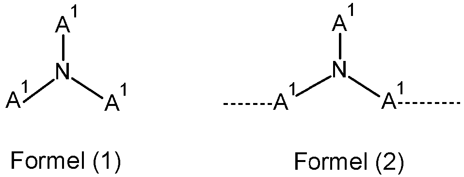 A1 bei jedem Auftreten gleich oder verschieden ein mono- oder polycyclisches, aromatisches oder heteroaromatisches Ringsystem mit 5 bis 60 aromatischen Ringatomen, vorzugsweise 5 bis 30 aromatischen Ringatomen, ist, das durch einen oder mehrere Reste R1 substituiert sein kann;R1 bei jedem Auftreten gleich oder verschieden H, D, F, Cl, Br, I, N(R2)2, CN, NO2, Si(R2)3, B(OR2)2, C(=O)R2, P(=O)(R2)2, S(=O)R2, S(=O)2R2, OSO2R2, eine geradkettige Alkyl-, Alkoxy- oder Thioalkoxygruppe mit 1 bis 40 C-Atomen oder eine verzweigte oder cyclische Alkyl-, Alkoxy- oder Thioalkoxygruppe mit 3 bis 40 C-Atomen, die jeweils durch einen oder mehrere Reste R2 substituiert sein kann, wobei eine oder mehrere nicht benachbarte CH2-Gruppen durch R2C=CR2, C=C, Si(R2)2, C=O, C=S, C=NR2, P(=O)(R2), SO, SO2, NR2, O, S oder CONR2 ersetzt sein können und wobei ein ein oder mehrere H-Atome durch D, F, Cl, Br, I oder CN ersetzt sein können, oder ein mono- oder polycyclisches, aromatisches oder heteroaromatisches Ringsystem mit 5 bis 60 aromatischen Ringatomen, das jeweils durch einen oder mehrere Reste R2 substituiert sein kann, oder eine Aryloxy- oder Heteroaryloxygruppe mit 5 bis 60 aromatischen Ringatomen, die durch einen oder mehrere Reste R2 substituiert sein kann, oder eine Aralkyl- oder Heteroaralkylgruppe mit 5 bis 60 aromatischen Ringatomen, die durch einen oder mehrere Reste R2 substituiert sein kann, oder eine Diarylaminogruppe, Diheteroarylaminogruppe oder Arylheteroarylaminogruppe mit 10 bis 40 aromatischen Ringatomen, die durch einen oder mehrere Reste R2 substituiert sein kann, ist, wobei zwei oder mehr Reste R1 hier auch ein mono- oder polycyclisches, aliphatisches oder aromatisches Ringsystem miteinander bilden können;R2 bei jedem Auftreten gleich oder verschieden H, D, F oder ein aliphatischer Kohlenwasserstoffrest mit 1 bis 20 C-Atomen, ein aromatischer und/oder ein heteroaromatischer Kohlenwasserstoffrest mit 5 bis 20 C-Atomen, worin zusätzlich ein oder mehrere H-Atome durch F ersetzt sein können, ist; wobei zwei oder mehr Substituenten R2 auch ein mono- oder polycyclisches, aliphatisches oder aromatisches Ringsystem miteinander bilden können; unddie gestrichelten Linien in Formel (2) Bindungen zu benachbarten Struktureinheiten in dem Polymer darstellen.
 - Organische Elektrolumineszenzvorrichtung nach irgendeinem der vorhergehenden Ansprüche, bei der die mindestens eine Lochtransportschicht mindestens ein Monotriarylamin enthält, das einer Verbindung einer der Formeln (T-1) bis (T-7)
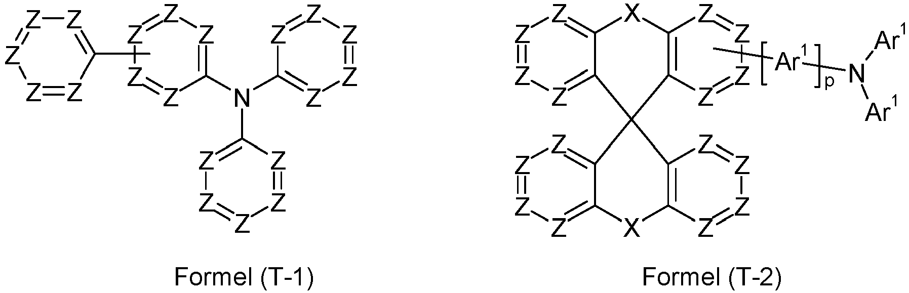


 Ar1 bei jedem Auftreten gleich oder verschieden ein mono- oder polycyclisches, aromatisches oder heteroaromatisches Ringsystem mit 5 bis 60 aromatischen Ringatomen ist, das durch einen oder mehrere Reste R1 substituiert sein kann;Z bei jedem Auftreten gleich oder verschieden N oder CR1 ist, wobei Z gleich C ist, wenn ein Substituent gebunden ist;X, Y bei jedem Auftreten gleich oder verschieden eine Einfachbindung, O, S, Se, BR1, C(R1)2, Si(R1)2, NR1, PR1, C(R1)2-C(R1)2 oder CR1=CR1 sind;E O, S, Se, BR1, C(R1)2, Si(R1)2, NR1, PR1, C(R1)2-C(R1)2 oder CR1=CR1 ist;i bei jedem Auftreten gleich oder verschieden 0 oder 1 ist, wobei die Summe aller i mindestens gleich 1 ist;p gleich 0 oder 1 ist;m, n gleich oder verschieden 0 oder 1 sind, wobei die Summe von m und n gleich 1 oder 2 ist.
 - Organische Elektrolumineszenzvorrichtung nach irgendeinem der vorhergehenden Ansprüche, bei der die mindestens eine Lochtransportschicht mindestens ein Monotriarylamin enthält, das einer Verbindung einer der Formeln (T-2-1) bis (T-2-4)


- Organische Elektrolumineszenzvorrichtung nach Anspruch 10, bei der das mindestens eine Monotriarylamin einer Verbindung der Formel (T-2-1) entspricht.
- Organische Elektrolumineszenzvorrichtung nach irgendeinem der Ansprüche 9 bis 11, bei der X eine Einfachbindung ist und Z C(R1)2 ist.
- Verfahren zur Herstellung einer organischen Elektrolumineszenzvorrichtung nach irgendeinem der vorhergehenden Ansprüche, das die folgenden Schritte umfasst:a. Abscheidung einer Lochinjektionsschicht enthaltend mindestens 90 Gew.-%, bezogen auf das Gesamtgewicht der Lochinjektionsschicht, mindestens eines Bismutkomplexes oder Galliumkomplexes auf einer Anode;b. Abscheidung mindestens einer Lochtransportschicht auf der Lochinjektionsschicht;c. Abscheidung mindestens einer emittierenden Schicht;d. Bildung einer Kathode.
- Verfahren nach Anspruch 13, bei dem die Lochinjektionsschicht, die Lochtransportschicht und die emittierende Schicht gleich oder verschieden über ein Aufdampfverfahren und/oder ein lösungsmittelbasiertes Verfahren abgeschieden werden.
Applications Claiming Priority (2)
| Application Number | Priority Date | Filing Date | Title |
|---|---|---|---|
| EP17158613 | 2017-03-01 | ||
| PCT/EP2018/054772 WO2018158232A1 (en) | 2017-03-01 | 2018-02-27 | Organic electroluminescent device |
Publications (2)
| Publication Number | Publication Date |
|---|---|
| EP3590141A1 EP3590141A1 (de) | 2020-01-08 |
| EP3590141B1 true EP3590141B1 (de) | 2025-04-30 |
Family
ID=58192230
Family Applications (1)
| Application Number | Title | Priority Date | Filing Date |
|---|---|---|---|
| EP18706527.1A Active EP3590141B1 (de) | 2017-03-01 | 2018-02-27 | Organische elektrolumineszente vorrichtung |
Country Status (6)
| Country | Link |
|---|---|
| US (1) | US11393987B2 (de) |
| EP (1) | EP3590141B1 (de) |
| JP (1) | JP2020511006A (de) |
| KR (2) | KR20190126097A (de) |
| CN (2) | CN117440703A (de) |
| WO (1) | WO2018158232A1 (de) |
Families Citing this family (7)
| Publication number | Priority date | Publication date | Assignee | Title |
|---|---|---|---|---|
| EP3590141B1 (de) | 2017-03-01 | 2025-04-30 | Merck Patent GmbH | Organische elektrolumineszente vorrichtung |
| EP3462516A1 (de) * | 2017-10-02 | 2019-04-03 | Novaled GmbH | Elektronische vorrichtung und verfahren zur herstellung davon |
| KR102315480B1 (ko) | 2019-06-28 | 2021-10-20 | 이데미쓰 고산 가부시키가이샤 | 화합물, 유기 전기발광 소자용 재료, 유기 전기발광 소자 및 전자 기기 |
| EP3859808B1 (de) | 2020-01-28 | 2025-12-24 | Novaled GmbH | Organische elektronische vorrichtung mit einer lochinjektionsschicht, die eine lochtransportverbindung umfasst |
| EP4225733B1 (de) * | 2020-10-09 | 2024-11-27 | Merck Patent GmbH | Verbindungen für elektronische vorrichtungen |
| KR20220090667A (ko) | 2020-12-22 | 2022-06-30 | 삼성디스플레이 주식회사 | 발광 소자 및 이를 포함한 전자 장치 |
| EP4152425A1 (de) * | 2021-09-20 | 2023-03-22 | Novaled GmbH | Organische elektronische vorrichtung mit einem substrat, einer anodenschicht, einer kathodenschicht, mindestens einer ersten emissionsschicht und einer lochinjektionsschicht, wobei die lochinjektionsschicht einen metallkomplex der formel (i) und eine verbindung der formel (ii) umfasst, wobei die lochinjektionsschicht zwischen der anodenschicht und der mindestens einen ersten emissionsschicht angeordnet ist |
Family Cites Families (92)
| Publication number | Priority date | Publication date | Assignee | Title |
|---|---|---|---|---|
| US5061569A (en) | 1990-07-26 | 1991-10-29 | Eastman Kodak Company | Electroluminescent device with organic electroluminescent medium |
| DE69432054T2 (de) | 1993-09-29 | 2003-10-09 | Idemitsu Kosan Co | Organische elektrolumineszenzelemente und arylendiaminderivate |
| JPH07133483A (ja) | 1993-11-09 | 1995-05-23 | Shinko Electric Ind Co Ltd | El素子用有機発光材料及びel素子 |
| EP0676461B1 (de) | 1994-04-07 | 2002-08-14 | Covion Organic Semiconductors GmbH | Spiroverbindungen und ihre Verwendung als Elektrolumineszenzmaterialien |
| JP3302945B2 (ja) | 1998-06-23 | 2002-07-15 | ネースディスプレイ・カンパニー・リミテッド | 新規な有機金属発光物質およびそれを含む有機電気発光素子 |
| ATE344532T1 (de) | 1999-05-13 | 2006-11-15 | Univ Princeton | Lichtemittierende, organische, auf elektrophosphoreszenz basierende anordnung mit sehr hoher quantenausbeute |
| EP2278637B2 (de) | 1999-12-01 | 2021-06-09 | The Trustees of Princeton University | Komplexe der Form L2MX |
| KR100377321B1 (ko) | 1999-12-31 | 2003-03-26 | 주식회사 엘지화학 | 피-형 반도체 성질을 갖는 유기 화합물을 포함하는 전기소자 |
| US6660410B2 (en) | 2000-03-27 | 2003-12-09 | Idemitsu Kosan Co., Ltd. | Organic electroluminescence element |
| US20020121638A1 (en) | 2000-06-30 | 2002-09-05 | Vladimir Grushin | Electroluminescent iridium compounds with fluorinated phenylpyridines, phenylpyrimidines, and phenylquinolines and devices made with such compounds |
| JP5241053B2 (ja) | 2000-08-11 | 2013-07-17 | ザ、トラスティーズ オブ プリンストン ユニバーシティ | 有機金属化合物及び放射移行有機電気燐光体 |
| JP4154140B2 (ja) | 2000-09-26 | 2008-09-24 | キヤノン株式会社 | 金属配位化合物 |
| JP4154138B2 (ja) | 2000-09-26 | 2008-09-24 | キヤノン株式会社 | 発光素子、表示装置及び金属配位化合物 |
| JP4154139B2 (ja) | 2000-09-26 | 2008-09-24 | キヤノン株式会社 | 発光素子 |
| KR100691543B1 (ko) | 2002-01-18 | 2007-03-09 | 주식회사 엘지화학 | 새로운 전자 수송용 물질 및 이를 이용한 유기 발광 소자 |
| ITRM20020411A1 (it) | 2002-08-01 | 2004-02-02 | Univ Roma La Sapienza | Derivati dello spirobifluorene, loro preparazione e loro uso. |
| KR20050057518A (ko) | 2002-09-20 | 2005-06-16 | 이데미쓰 고산 가부시키가이샤 | 유기 전기발광 소자 |
| KR101030158B1 (ko) | 2002-12-23 | 2011-04-18 | 메르크 파텐트 게엠베하 | 유기 전자발광 부품 |
| DE10310887A1 (de) | 2003-03-11 | 2004-09-30 | Covion Organic Semiconductors Gmbh | Matallkomplexe |
| JP4185097B2 (ja) | 2003-03-13 | 2008-11-19 | 出光興産株式会社 | 新規含窒素複素環誘導体及びそれを用いた有機エレクトロルミネッセンス素子 |
| JP4411851B2 (ja) | 2003-03-19 | 2010-02-10 | コニカミノルタホールディングス株式会社 | 有機エレクトロルミネッセンス素子 |
| EP1717291A3 (de) | 2003-04-15 | 2007-03-21 | Merck Patent GmbH | Mischungen von organischen, zur Emission befähigten Halbleitern und Maxtrixmaterialien, deren Verwendung und diese Mischungen enthaltende Elektronikbauteile |
| JP4635870B2 (ja) | 2003-04-23 | 2011-02-23 | コニカミノルタホールディングス株式会社 | 有機エレクトロルミネッセンス素子、照明装置及び表示装置 |
| EP2229039B1 (de) * | 2003-07-02 | 2012-02-29 | Idemitsu Kosan Co., Ltd. | Organische elektrolummineszente Vorrichtung und Anzeigegerät mit dieser |
| DE10333232A1 (de) | 2003-07-21 | 2007-10-11 | Merck Patent Gmbh | Organisches Elektrolumineszenzelement |
| DE10338550A1 (de) | 2003-08-19 | 2005-03-31 | Basf Ag | Übergangsmetallkomplexe mit Carbenliganden als Emitter für organische Licht-emittierende Dioden (OLEDs) |
| DE10345572A1 (de) | 2003-09-29 | 2005-05-19 | Covion Organic Semiconductors Gmbh | Metallkomplexe |
| US7795801B2 (en) | 2003-09-30 | 2010-09-14 | Konica Minolta Holdings, Inc. | Organic electroluminescent element, illuminator, display and compound |
| DE102004008304A1 (de) | 2004-02-20 | 2005-09-08 | Covion Organic Semiconductors Gmbh | Organische elektronische Vorrichtungen |
| US7790890B2 (en) | 2004-03-31 | 2010-09-07 | Konica Minolta Holdings, Inc. | Organic electroluminescence element material, organic electroluminescence element, display device and illumination device |
| KR100787425B1 (ko) | 2004-11-29 | 2007-12-26 | 삼성에스디아이 주식회사 | 페닐카바졸계 화합물 및 이를 이용한 유기 전계 발광 소자 |
| DE102004023277A1 (de) | 2004-05-11 | 2005-12-01 | Covion Organic Semiconductors Gmbh | Neue Materialmischungen für die Elektrolumineszenz |
| US7598388B2 (en) | 2004-05-18 | 2009-10-06 | The University Of Southern California | Carbene containing metal complexes as OLEDs |
| JP4862248B2 (ja) | 2004-06-04 | 2012-01-25 | コニカミノルタホールディングス株式会社 | 有機エレクトロルミネッセンス素子、照明装置及び表示装置 |
| ITRM20040352A1 (it) | 2004-07-15 | 2004-10-15 | Univ Roma La Sapienza | Derivati oligomerici dello spirobifluorene, loro preparazione e loro uso. |
| EP1655359A1 (de) | 2004-11-06 | 2006-05-10 | Covion Organic Semiconductors GmbH | Organische Elektrolumineszenzvorrichtung |
| US20090066225A1 (en) | 2005-03-18 | 2009-03-12 | Idemitsu Kosan Co., Ltd. | Aromatic amine derivative and organic electroluminescence device utilizing the same |
| CN101155895B (zh) | 2005-04-14 | 2011-12-28 | 默克专利有限公司 | 用于有机电子器件的化合物 |
| KR101289923B1 (ko) | 2005-05-03 | 2013-07-25 | 메르크 파텐트 게엠베하 | 유기 전계발광 장치 및 그에 사용되는 붕산 및 보린산유도체 |
| DE102005023437A1 (de) | 2005-05-20 | 2006-11-30 | Merck Patent Gmbh | Verbindungen für organische elektronische Vorrichtungen |
| US7993760B2 (en) | 2005-12-01 | 2011-08-09 | Nippon Steel Chemical Co., Ltd. | Compound for use in organic electroluminescent device and organic electroluminescent device |
| EP1806795B1 (de) | 2005-12-21 | 2008-07-09 | Novaled AG | Organisches Bauelement |
| DE102006025777A1 (de) | 2006-05-31 | 2007-12-06 | Merck Patent Gmbh | Neue Materialien für organische Elektrolumineszenzvorrichtungen |
| DE102006025846A1 (de) | 2006-06-02 | 2007-12-06 | Merck Patent Gmbh | Neue Materialien für organische Elektrolumineszenzvorrichtungen |
| DE102006031990A1 (de) | 2006-07-11 | 2008-01-17 | Merck Patent Gmbh | Neue Materialien für organische Elektrolumineszenzvorrichtungen |
| EP2080762B1 (de) | 2006-11-09 | 2016-09-14 | Nippon Steel & Sumikin Chemical Co., Ltd. | Verbindung für organische elektrolumineszenzvorrichtung und organische elektrolumineszenzvorrichtung |
| DE102007002714A1 (de) | 2007-01-18 | 2008-07-31 | Merck Patent Gmbh | Neue Materialien für organische Elektrolumineszenzvorrichtungen |
| DE102007018456B4 (de) | 2007-04-19 | 2022-02-24 | Novaled Gmbh | Verwendung von Hauptgruppenelementhalogeniden und/oder -pseudohalogeniden, organisches halbleitendes Matrixmaterial, elektronische und optoelektronische Bauelemente |
| DE102007024850A1 (de) | 2007-05-29 | 2008-12-04 | Merck Patent Gmbh | Neue Materialien für organische Elektrolumineszenzvorrichtungen |
| DE102007053771A1 (de) | 2007-11-12 | 2009-05-14 | Merck Patent Gmbh | Organische Elektrolumineszenzvorrichtungen |
| US7862908B2 (en) | 2007-11-26 | 2011-01-04 | National Tsing Hua University | Conjugated compounds containing hydroindoloacridine structural elements, and their use |
| DE102008033943A1 (de) | 2008-07-18 | 2010-01-21 | Merck Patent Gmbh | Neue Materialien für organische Elektrolumineszenzvorrichtungen |
| DE102008035413A1 (de) | 2008-07-29 | 2010-02-04 | Merck Patent Gmbh | Verbindungen für organische elektronische Vorrichtungen |
| DE102008036982A1 (de) | 2008-08-08 | 2010-02-11 | Merck Patent Gmbh | Organische Elektrolumineszenzvorrichtung |
| KR101506919B1 (ko) | 2008-10-31 | 2015-03-30 | 롬엔드하스전자재료코리아유한회사 | 신규한 유기 전자재료용 화합물 및 이를 포함하는 유기 전자 소자 |
| DE102008056688A1 (de) | 2008-11-11 | 2010-05-12 | Merck Patent Gmbh | Materialien für organische Elektrolumineszenzvorrichtungen |
| EP2344607B1 (de) | 2008-11-11 | 2013-04-10 | Merck Patent GmbH | Organische elektrolumineszenzvorrichtungen |
| DE102008064200A1 (de) | 2008-12-22 | 2010-07-01 | Merck Patent Gmbh | Organische Elektrolumineszenzvorrichtung |
| DE102009014513A1 (de) | 2009-03-23 | 2010-09-30 | Merck Patent Gmbh | Organische Elektrolumineszenzvorrichtung |
| DE102009023155A1 (de) | 2009-05-29 | 2010-12-02 | Merck Patent Gmbh | Materialien für organische Elektrolumineszenzvorrichtungen |
| DE102009031021A1 (de) | 2009-06-30 | 2011-01-05 | Merck Patent Gmbh | Materialien für organische Elektrolumineszenzvorrichtungen |
| DE102009041289A1 (de) * | 2009-09-16 | 2011-03-17 | Merck Patent Gmbh | Organische Elektrolumineszenzvorrichtung |
| DE102009048791A1 (de) | 2009-10-08 | 2011-04-14 | Merck Patent Gmbh | Materialien für organische Elektrolumineszenzvorrichtungen |
| DE102010005697A1 (de) | 2010-01-25 | 2011-07-28 | Merck Patent GmbH, 64293 | Verbindungen für elektronische Vorrichtungen |
| DE102010012738A1 (de) | 2010-03-25 | 2011-09-29 | Merck Patent Gmbh | Materialien für organische Elektrolumineszenzvorrichtungen |
| DE102010019306B4 (de) | 2010-05-04 | 2021-05-20 | Merck Patent Gmbh | Organische Elektrolumineszenzvorrichtungen |
| DE102010045405A1 (de) | 2010-09-15 | 2012-03-15 | Merck Patent Gmbh | Materialien für organische Elektrolumineszenzvorrichtungen |
| DE102010048608A1 (de) | 2010-10-15 | 2012-04-19 | Merck Patent Gmbh | Materialien für organische Elektrolumineszenzvorrichtungen |
| DE102010048607A1 (de) | 2010-10-15 | 2012-04-19 | Merck Patent Gmbh | Verbindungen für elektronische Vorrichtungen |
| CN103534331B (zh) * | 2011-03-29 | 2016-06-08 | 大州电子材料株式会社 | 萘衍生物、包括其的有机材料及包括其的有机电致发光元件 |
| US9620722B2 (en) | 2011-04-18 | 2017-04-11 | Merck Patent Gmbh | Materials for organic electroluminescent devices |
| EP2705552B1 (de) | 2011-05-05 | 2015-03-04 | Merck Patent GmbH | Verbindungen für elektronische vorrichtungen |
| CN103842339B (zh) | 2011-09-21 | 2017-08-08 | 默克专利有限公司 | 用于有机电致发光器件的咔唑衍生物 |
| CN103946215B (zh) | 2011-11-17 | 2016-09-28 | 默克专利有限公司 | 螺二氢吖啶衍生物和其作为有机电致发光器件用材料的用途 |
| DE102012204327A1 (de) * | 2012-03-19 | 2013-09-19 | Osram Opto Semiconductors Gmbh | Optoelektronisches Bauelement und Verfahren zum Herstellen eines optoelektronischen Bauelements |
| DE102012208235B4 (de) * | 2012-05-16 | 2021-05-12 | Osram Oled Gmbh | Optoelektronisches Bauelement und Verfahren zum Herstellen eines optoelektronischen Bauelements |
| DE102012209523A1 (de) | 2012-06-06 | 2013-12-12 | Osram Opto Semiconductors Gmbh | Hauptgruppenmetallkomplexe als p-Dotanden für organische elektronische Matrixmaterialien |
| DE112013002910T5 (de) | 2012-06-12 | 2015-03-19 | Merck Patent Gmbh | Verbindungen für elektronische Vorrichtungen |
| KR102583348B1 (ko) | 2012-07-23 | 2023-09-26 | 메르크 파텐트 게엠베하 | 화합물 및 유기 전계 발광 디바이스 |
| US9768391B2 (en) | 2012-07-23 | 2017-09-19 | Merck Patent Gmbh | Derivatives of 2-diarylaminofluorene and organic electronic compounds containing them |
| KR20240130142A (ko) | 2012-07-23 | 2024-08-28 | 메르크 파텐트 게엠베하 | 플루오렌 및 이를 함유하는 전자 소자 |
| DE102012214021B4 (de) | 2012-08-08 | 2018-05-09 | Osram Oled Gmbh | Optoelektronisches Bauelement und Verfahren zum Herstellen eines optoelektronischen Bauelementes |
| KR102143742B1 (ko) | 2012-09-04 | 2020-08-12 | 메르크 파텐트 게엠베하 | 전자 소자용 접속부 |
| JP6449162B2 (ja) | 2012-10-09 | 2019-01-09 | メルク パテント ゲーエムベーハー | 電子素子 |
| EP2941472B1 (de) | 2013-01-03 | 2018-07-25 | Merck Patent GmbH | Materialien für elektronische vorrichtungen |
| DE102013215342B4 (de) * | 2013-08-05 | 2023-05-04 | Novaled Gmbh | Verfahren zur Herstellung organisch phosphoreszenter Schichten unter Zusatz schwerer Hauptgruppenmetallkomplexe, damit hergestellte Schicht, deren Verwendung und organisches Halbleiterbauelement diese umfassend |
| CN105636944B (zh) | 2013-10-14 | 2019-03-01 | 默克专利有限公司 | 用于电子器件的材料 |
| US10741772B2 (en) * | 2014-08-29 | 2020-08-11 | Samsung Electronics Co., Ltd. | Organic light-emitting device |
| WO2016062368A1 (de) * | 2014-10-24 | 2016-04-28 | Merck Patent Gmbh | Materialien für elektronische vorrichtungen |
| US10651388B2 (en) * | 2014-12-30 | 2020-05-12 | Merck Patent Gmbh | Compositions comprising at least one polymer and at least one metal complex and to electroluminescent devices containing said compositions |
| CN107667439B (zh) * | 2015-05-22 | 2021-01-05 | 默克专利有限公司 | 包含有机半导体和金属络合物的制剂 |
| EP3590141B1 (de) | 2017-03-01 | 2025-04-30 | Merck Patent GmbH | Organische elektrolumineszente vorrichtung |
-
2018
- 2018-02-27 EP EP18706527.1A patent/EP3590141B1/de active Active
- 2018-02-27 KR KR1020197028574A patent/KR20190126097A/ko not_active Ceased
- 2018-02-27 US US16/489,728 patent/US11393987B2/en active Active
- 2018-02-27 CN CN202311271580.3A patent/CN117440703A/zh active Pending
- 2018-02-27 CN CN201880008450.1A patent/CN110268544A/zh active Pending
- 2018-02-27 JP JP2019547692A patent/JP2020511006A/ja active Pending
- 2018-02-27 KR KR1020237042650A patent/KR20230170828A/ko active Pending
- 2018-02-27 WO PCT/EP2018/054772 patent/WO2018158232A1/en not_active Ceased
Also Published As
| Publication number | Publication date |
|---|---|
| US20190372025A1 (en) | 2019-12-05 |
| KR20190126097A (ko) | 2019-11-08 |
| EP3590141A1 (de) | 2020-01-08 |
| KR20230170828A (ko) | 2023-12-19 |
| JP2020511006A (ja) | 2020-04-09 |
| US11393987B2 (en) | 2022-07-19 |
| CN110268544A (zh) | 2019-09-20 |
| WO2018158232A1 (en) | 2018-09-07 |
| CN117440703A (zh) | 2024-01-23 |
Similar Documents
| Publication | Publication Date | Title |
|---|---|---|
| US10270052B2 (en) | Electronic device | |
| US12351594B2 (en) | Materials for organic electroluminescent devices | |
| US9871201B2 (en) | Electronic devices | |
| EP3274419B1 (de) | Materialien für organische elektrolumineszenzvorrichtungen | |
| US9434877B2 (en) | Organic electroluminescent device | |
| US10193094B2 (en) | Organic light-emitting device having delayed fluorescence | |
| US10454040B2 (en) | Materials for electronic devices | |
| US10249828B2 (en) | Organic electroluminescent device | |
| EP3590141B1 (de) | Organische elektrolumineszente vorrichtung | |
| US10407394B2 (en) | Triarylamine-substituted benzo[H]quinoline-derivatives as materials for electronic devices | |
| US20220048836A1 (en) | Materials for organic electroluminescent devices | |
| US20230016716A1 (en) | Materials for organic electroluminescent devices | |
| KR20210096630A (ko) | 전자 디바이스 | |
| US11631816B2 (en) | Electronic device | |
| EP3642185B1 (de) | Materialien für organische elektrolumineszenzvorrichtungen | |
| US20150340636A1 (en) | Electronic Device | |
| US9246118B2 (en) | Organic electroluminescent device | |
| EP4045483B1 (de) | Materialien für organische elektrolumineszente vorrichtungen |
Legal Events
| Date | Code | Title | Description |
|---|---|---|---|
| STAA | Information on the status of an ep patent application or granted ep patent |
Free format text: STATUS: UNKNOWN |
|
| STAA | Information on the status of an ep patent application or granted ep patent |
Free format text: STATUS: THE INTERNATIONAL PUBLICATION HAS BEEN MADE |
|
| PUAI | Public reference made under article 153(3) epc to a published international application that has entered the european phase |
Free format text: ORIGINAL CODE: 0009012 |
|
| STAA | Information on the status of an ep patent application or granted ep patent |
Free format text: STATUS: REQUEST FOR EXAMINATION WAS MADE |
|
| 17P | Request for examination filed |
Effective date: 20190822 |
|
| AK | Designated contracting states |
Kind code of ref document: A1 Designated state(s): AL AT BE BG CH CY CZ DE DK EE ES FI FR GB GR HR HU IE IS IT LI LT LU LV MC MK MT NL NO PL PT RO RS SE SI SK SM TR |
|
| AX | Request for extension of the european patent |
Extension state: BA ME |
|
| DAV | Request for validation of the european patent (deleted) | ||
| DAX | Request for extension of the european patent (deleted) | ||
| STAA | Information on the status of an ep patent application or granted ep patent |
Free format text: STATUS: EXAMINATION IS IN PROGRESS |
|
| 17Q | First examination report despatched |
Effective date: 20220104 |
|
| RAP3 | Party data changed (applicant data changed or rights of an application transferred) |
Owner name: MERCK PATENT GMBH |
|
| P01 | Opt-out of the competence of the unified patent court (upc) registered |
Effective date: 20230519 |
|
| REG | Reference to a national code |
Ref country code: DE Ref legal event code: R079 Free format text: PREVIOUS MAIN CLASS: H01L0051540000 Ipc: H10K0085300000 Ref country code: DE Ref legal event code: R079 Ref document number: 602018081484 Country of ref document: DE Free format text: PREVIOUS MAIN CLASS: H01L0051540000 Ipc: H10K0085300000 |
|
| GRAP | Despatch of communication of intention to grant a patent |
Free format text: ORIGINAL CODE: EPIDOSNIGR1 |
|
| STAA | Information on the status of an ep patent application or granted ep patent |
Free format text: STATUS: GRANT OF PATENT IS INTENDED |
|
| RIC1 | Information provided on ipc code assigned before grant |
Ipc: H10K 102/00 20230101ALN20250110BHEP Ipc: H10K 50/17 20230101ALN20250110BHEP Ipc: H10K 85/30 20230101AFI20250110BHEP |
|
| RIC1 | Information provided on ipc code assigned before grant |
Ipc: H10K 102/00 20230101ALN20250117BHEP Ipc: H10K 50/17 20230101ALN20250117BHEP Ipc: H10K 85/30 20230101AFI20250117BHEP |
|
| INTG | Intention to grant announced |
Effective date: 20250131 |
|
| GRAS | Grant fee paid |
Free format text: ORIGINAL CODE: EPIDOSNIGR3 |
|
| GRAA | (expected) grant |
Free format text: ORIGINAL CODE: 0009210 |
|
| STAA | Information on the status of an ep patent application or granted ep patent |
Free format text: STATUS: THE PATENT HAS BEEN GRANTED |
|
| AK | Designated contracting states |
Kind code of ref document: B1 Designated state(s): AL AT BE BG CH CY CZ DE DK EE ES FI FR GB GR HR HU IE IS IT LI LT LU LV MC MK MT NL NO PL PT RO RS SE SI SK SM TR |
|
| REG | Reference to a national code |
Ref country code: CH Ref legal event code: EP Ref country code: GB Ref legal event code: FG4D |
|
| REG | Reference to a national code |
Ref country code: IE Ref legal event code: FG4D |
|
| REG | Reference to a national code |
Ref country code: DE Ref legal event code: R096 Ref document number: 602018081484 Country of ref document: DE |
|
| REG | Reference to a national code |
Ref country code: NL Ref legal event code: MP Effective date: 20250430 |
|
| REG | Reference to a national code |
Ref country code: AT Ref legal event code: MK05 Ref document number: 1791349 Country of ref document: AT Kind code of ref document: T Effective date: 20250430 |
|
| PG25 | Lapsed in a contracting state [announced via postgrant information from national office to epo] |
Ref country code: FI Free format text: LAPSE BECAUSE OF FAILURE TO SUBMIT A TRANSLATION OF THE DESCRIPTION OR TO PAY THE FEE WITHIN THE PRESCRIBED TIME-LIMIT Effective date: 20250430 Ref country code: PT Free format text: LAPSE BECAUSE OF FAILURE TO SUBMIT A TRANSLATION OF THE DESCRIPTION OR TO PAY THE FEE WITHIN THE PRESCRIBED TIME-LIMIT Effective date: 20250901 Ref country code: ES Free format text: LAPSE BECAUSE OF FAILURE TO SUBMIT A TRANSLATION OF THE DESCRIPTION OR TO PAY THE FEE WITHIN THE PRESCRIBED TIME-LIMIT Effective date: 20250430 |
|
| REG | Reference to a national code |
Ref country code: LT Ref legal event code: MG9D |
|
| PG25 | Lapsed in a contracting state [announced via postgrant information from national office to epo] |
Ref country code: NO Free format text: LAPSE BECAUSE OF FAILURE TO SUBMIT A TRANSLATION OF THE DESCRIPTION OR TO PAY THE FEE WITHIN THE PRESCRIBED TIME-LIMIT Effective date: 20250730 Ref country code: GR Free format text: LAPSE BECAUSE OF FAILURE TO SUBMIT A TRANSLATION OF THE DESCRIPTION OR TO PAY THE FEE WITHIN THE PRESCRIBED TIME-LIMIT Effective date: 20250731 |
|
| PG25 | Lapsed in a contracting state [announced via postgrant information from national office to epo] |
Ref country code: PL Free format text: LAPSE BECAUSE OF FAILURE TO SUBMIT A TRANSLATION OF THE DESCRIPTION OR TO PAY THE FEE WITHIN THE PRESCRIBED TIME-LIMIT Effective date: 20250430 Ref country code: NL Free format text: LAPSE BECAUSE OF FAILURE TO SUBMIT A TRANSLATION OF THE DESCRIPTION OR TO PAY THE FEE WITHIN THE PRESCRIBED TIME-LIMIT Effective date: 20250430 |
|
| PG25 | Lapsed in a contracting state [announced via postgrant information from national office to epo] |
Ref country code: BG Free format text: LAPSE BECAUSE OF FAILURE TO SUBMIT A TRANSLATION OF THE DESCRIPTION OR TO PAY THE FEE WITHIN THE PRESCRIBED TIME-LIMIT Effective date: 20250430 |
|
| PG25 | Lapsed in a contracting state [announced via postgrant information from national office to epo] |
Ref country code: HR Free format text: LAPSE BECAUSE OF FAILURE TO SUBMIT A TRANSLATION OF THE DESCRIPTION OR TO PAY THE FEE WITHIN THE PRESCRIBED TIME-LIMIT Effective date: 20250430 |
|
| PG25 | Lapsed in a contracting state [announced via postgrant information from national office to epo] |
Ref country code: AT Free format text: LAPSE BECAUSE OF FAILURE TO SUBMIT A TRANSLATION OF THE DESCRIPTION OR TO PAY THE FEE WITHIN THE PRESCRIBED TIME-LIMIT Effective date: 20250430 |
|
| PG25 | Lapsed in a contracting state [announced via postgrant information from national office to epo] |
Ref country code: RS Free format text: LAPSE BECAUSE OF FAILURE TO SUBMIT A TRANSLATION OF THE DESCRIPTION OR TO PAY THE FEE WITHIN THE PRESCRIBED TIME-LIMIT Effective date: 20250731 |
|
| PG25 | Lapsed in a contracting state [announced via postgrant information from national office to epo] |
Ref country code: IS Free format text: LAPSE BECAUSE OF FAILURE TO SUBMIT A TRANSLATION OF THE DESCRIPTION OR TO PAY THE FEE WITHIN THE PRESCRIBED TIME-LIMIT Effective date: 20250830 |
|
| PG25 | Lapsed in a contracting state [announced via postgrant information from national office to epo] |
Ref country code: LV Free format text: LAPSE BECAUSE OF FAILURE TO SUBMIT A TRANSLATION OF THE DESCRIPTION OR TO PAY THE FEE WITHIN THE PRESCRIBED TIME-LIMIT Effective date: 20250430 |