EP3584629B1 - Vorrichtung zur identifizierung eines bindungsetiketts und vorrichtung zur bindung - Google Patents
Vorrichtung zur identifizierung eines bindungsetiketts und vorrichtung zur bindung Download PDFInfo
- Publication number
- EP3584629B1 EP3584629B1 EP17847702.2A EP17847702A EP3584629B1 EP 3584629 B1 EP3584629 B1 EP 3584629B1 EP 17847702 A EP17847702 A EP 17847702A EP 3584629 B1 EP3584629 B1 EP 3584629B1
- Authority
- EP
- European Patent Office
- Prior art keywords
- binding
- binding marker
- identifying
- marker
- electrically conductive
- Prior art date
- Legal status (The legal status is an assumption and is not a legal conclusion. Google has not performed a legal analysis and makes no representation as to the accuracy of the status listed.)
- Not-in-force
Links
Images
Classifications
-
- G—PHYSICS
- G02—OPTICS
- G02F—OPTICAL DEVICES OR ARRANGEMENTS FOR THE CONTROL OF LIGHT BY MODIFICATION OF THE OPTICAL PROPERTIES OF THE MEDIA OF THE ELEMENTS INVOLVED THEREIN; NON-LINEAR OPTICS; FREQUENCY-CHANGING OF LIGHT; OPTICAL LOGIC ELEMENTS; OPTICAL ANALOGUE/DIGITAL CONVERTERS
- G02F1/00—Devices or arrangements for the control of the intensity, colour, phase, polarisation or direction of light arriving from an independent light source, e.g. switching, gating or modulating; Non-linear optics
- G02F1/01—Devices or arrangements for the control of the intensity, colour, phase, polarisation or direction of light arriving from an independent light source, e.g. switching, gating or modulating; Non-linear optics for the control of the intensity, phase, polarisation or colour
- G02F1/13—Devices or arrangements for the control of the intensity, colour, phase, polarisation or direction of light arriving from an independent light source, e.g. switching, gating or modulating; Non-linear optics for the control of the intensity, phase, polarisation or colour based on liquid crystals, e.g. single liquid crystal display cells
- G02F1/133—Constructional arrangements; Operation of liquid crystal cells; Circuit arrangements
- G02F1/1333—Constructional arrangements; Manufacturing methods
- G02F1/133308—Support structures for LCD panels, e.g. frames or bezels
-
- G—PHYSICS
- G02—OPTICS
- G02F—OPTICAL DEVICES OR ARRANGEMENTS FOR THE CONTROL OF LIGHT BY MODIFICATION OF THE OPTICAL PROPERTIES OF THE MEDIA OF THE ELEMENTS INVOLVED THEREIN; NON-LINEAR OPTICS; FREQUENCY-CHANGING OF LIGHT; OPTICAL LOGIC ELEMENTS; OPTICAL ANALOGUE/DIGITAL CONVERTERS
- G02F1/00—Devices or arrangements for the control of the intensity, colour, phase, polarisation or direction of light arriving from an independent light source, e.g. switching, gating or modulating; Non-linear optics
- G02F1/01—Devices or arrangements for the control of the intensity, colour, phase, polarisation or direction of light arriving from an independent light source, e.g. switching, gating or modulating; Non-linear optics for the control of the intensity, phase, polarisation or colour
- G02F1/13—Devices or arrangements for the control of the intensity, colour, phase, polarisation or direction of light arriving from an independent light source, e.g. switching, gating or modulating; Non-linear optics for the control of the intensity, phase, polarisation or colour based on liquid crystals, e.g. single liquid crystal display cells
- G02F1/1303—Apparatus specially adapted to the manufacture of LCDs
-
- G—PHYSICS
- G02—OPTICS
- G02F—OPTICAL DEVICES OR ARRANGEMENTS FOR THE CONTROL OF LIGHT BY MODIFICATION OF THE OPTICAL PROPERTIES OF THE MEDIA OF THE ELEMENTS INVOLVED THEREIN; NON-LINEAR OPTICS; FREQUENCY-CHANGING OF LIGHT; OPTICAL LOGIC ELEMENTS; OPTICAL ANALOGUE/DIGITAL CONVERTERS
- G02F1/00—Devices or arrangements for the control of the intensity, colour, phase, polarisation or direction of light arriving from an independent light source, e.g. switching, gating or modulating; Non-linear optics
- G02F1/01—Devices or arrangements for the control of the intensity, colour, phase, polarisation or direction of light arriving from an independent light source, e.g. switching, gating or modulating; Non-linear optics for the control of the intensity, phase, polarisation or colour
- G02F1/13—Devices or arrangements for the control of the intensity, colour, phase, polarisation or direction of light arriving from an independent light source, e.g. switching, gating or modulating; Non-linear optics for the control of the intensity, phase, polarisation or colour based on liquid crystals, e.g. single liquid crystal display cells
- G02F1/133—Constructional arrangements; Operation of liquid crystal cells; Circuit arrangements
- G02F1/1333—Constructional arrangements; Manufacturing methods
- G02F1/133345—Insulating layers
-
- G—PHYSICS
- G02—OPTICS
- G02F—OPTICAL DEVICES OR ARRANGEMENTS FOR THE CONTROL OF LIGHT BY MODIFICATION OF THE OPTICAL PROPERTIES OF THE MEDIA OF THE ELEMENTS INVOLVED THEREIN; NON-LINEAR OPTICS; FREQUENCY-CHANGING OF LIGHT; OPTICAL LOGIC ELEMENTS; OPTICAL ANALOGUE/DIGITAL CONVERTERS
- G02F1/00—Devices or arrangements for the control of the intensity, colour, phase, polarisation or direction of light arriving from an independent light source, e.g. switching, gating or modulating; Non-linear optics
- G02F1/01—Devices or arrangements for the control of the intensity, colour, phase, polarisation or direction of light arriving from an independent light source, e.g. switching, gating or modulating; Non-linear optics for the control of the intensity, phase, polarisation or colour
- G02F1/13—Devices or arrangements for the control of the intensity, colour, phase, polarisation or direction of light arriving from an independent light source, e.g. switching, gating or modulating; Non-linear optics for the control of the intensity, phase, polarisation or colour based on liquid crystals, e.g. single liquid crystal display cells
- G02F1/133—Constructional arrangements; Operation of liquid crystal cells; Circuit arrangements
- G02F1/1333—Constructional arrangements; Manufacturing methods
- G02F1/133354—Arrangements for aligning or assembling substrates
-
- G—PHYSICS
- G02—OPTICS
- G02F—OPTICAL DEVICES OR ARRANGEMENTS FOR THE CONTROL OF LIGHT BY MODIFICATION OF THE OPTICAL PROPERTIES OF THE MEDIA OF THE ELEMENTS INVOLVED THEREIN; NON-LINEAR OPTICS; FREQUENCY-CHANGING OF LIGHT; OPTICAL LOGIC ELEMENTS; OPTICAL ANALOGUE/DIGITAL CONVERTERS
- G02F1/00—Devices or arrangements for the control of the intensity, colour, phase, polarisation or direction of light arriving from an independent light source, e.g. switching, gating or modulating; Non-linear optics
- G02F1/01—Devices or arrangements for the control of the intensity, colour, phase, polarisation or direction of light arriving from an independent light source, e.g. switching, gating or modulating; Non-linear optics for the control of the intensity, phase, polarisation or colour
- G02F1/13—Devices or arrangements for the control of the intensity, colour, phase, polarisation or direction of light arriving from an independent light source, e.g. switching, gating or modulating; Non-linear optics for the control of the intensity, phase, polarisation or colour based on liquid crystals, e.g. single liquid crystal display cells
- G02F1/133—Constructional arrangements; Operation of liquid crystal cells; Circuit arrangements
- G02F1/1333—Constructional arrangements; Manufacturing methods
- G02F1/1335—Structural association of cells with optical devices, e.g. polarisers or reflectors
- G02F1/133509—Filters, e.g. light shielding masks
- G02F1/133512—Light shielding layers, e.g. black matrix
-
- G—PHYSICS
- G02—OPTICS
- G02F—OPTICAL DEVICES OR ARRANGEMENTS FOR THE CONTROL OF LIGHT BY MODIFICATION OF THE OPTICAL PROPERTIES OF THE MEDIA OF THE ELEMENTS INVOLVED THEREIN; NON-LINEAR OPTICS; FREQUENCY-CHANGING OF LIGHT; OPTICAL LOGIC ELEMENTS; OPTICAL ANALOGUE/DIGITAL CONVERTERS
- G02F1/00—Devices or arrangements for the control of the intensity, colour, phase, polarisation or direction of light arriving from an independent light source, e.g. switching, gating or modulating; Non-linear optics
- G02F1/01—Devices or arrangements for the control of the intensity, colour, phase, polarisation or direction of light arriving from an independent light source, e.g. switching, gating or modulating; Non-linear optics for the control of the intensity, phase, polarisation or colour
- G02F1/13—Devices or arrangements for the control of the intensity, colour, phase, polarisation or direction of light arriving from an independent light source, e.g. switching, gating or modulating; Non-linear optics for the control of the intensity, phase, polarisation or colour based on liquid crystals, e.g. single liquid crystal display cells
- G02F1/133—Constructional arrangements; Operation of liquid crystal cells; Circuit arrangements
- G02F1/1333—Constructional arrangements; Manufacturing methods
- G02F1/1335—Structural association of cells with optical devices, e.g. polarisers or reflectors
- G02F1/13356—Structural association of cells with optical devices, e.g. polarisers or reflectors characterised by the placement of the optical elements
- G02F1/133562—Structural association of cells with optical devices, e.g. polarisers or reflectors characterised by the placement of the optical elements on the viewer side
-
- G—PHYSICS
- G02—OPTICS
- G02F—OPTICAL DEVICES OR ARRANGEMENTS FOR THE CONTROL OF LIGHT BY MODIFICATION OF THE OPTICAL PROPERTIES OF THE MEDIA OF THE ELEMENTS INVOLVED THEREIN; NON-LINEAR OPTICS; FREQUENCY-CHANGING OF LIGHT; OPTICAL LOGIC ELEMENTS; OPTICAL ANALOGUE/DIGITAL CONVERTERS
- G02F1/00—Devices or arrangements for the control of the intensity, colour, phase, polarisation or direction of light arriving from an independent light source, e.g. switching, gating or modulating; Non-linear optics
- G02F1/01—Devices or arrangements for the control of the intensity, colour, phase, polarisation or direction of light arriving from an independent light source, e.g. switching, gating or modulating; Non-linear optics for the control of the intensity, phase, polarisation or colour
- G02F1/13—Devices or arrangements for the control of the intensity, colour, phase, polarisation or direction of light arriving from an independent light source, e.g. switching, gating or modulating; Non-linear optics for the control of the intensity, phase, polarisation or colour based on liquid crystals, e.g. single liquid crystal display cells
- G02F1/133—Constructional arrangements; Operation of liquid crystal cells; Circuit arrangements
- G02F1/1333—Constructional arrangements; Manufacturing methods
- G02F1/1345—Conductors connecting electrodes to cell terminals
- G02F1/13452—Conductors connecting driver circuitry and terminals of panels
Definitions
- the disclosure relates to the field of display technology, and in particular, to an apparatus for identifying an electrically conductive binding marker of a display panel and a device for binding.
- the four sides of the liquid crystal panel of a liquid crystal display are wrapped by an outer frame, which is generally assembled with the rear shell of the display.
- the array substrate (TFT substrate) of the liquid crystal panel is set close to the backlight, and the color film substrate (CF substrate) is located on a side of the array substrate away from the backlight.
- CF substrate color film substrate
- a liquid crystal display which is frameless on four sides does not contain the outer frame, and the liquid crystal panel is adhered to the middle frame 71 of the backlight 7 by a double-sided adhesive 9, so as to implement the frameless structure of the liquid crystal display.
- the color film substrate 51 (CF substrate) of the frameless liquid crystal display is set close to the backlight 7, and the array substrate 52 (TFT substrate) is located on a side of the color film substrate 51 away from the backlight 7, and such a structure causes the flexible printed circuit board 8 bound on the array substrate 52 to be wrapped inside the whole display structure, thereby keeping the overall appearance of the liquid crystal display as a frameless structure.
- the color film substrate 51 (CF substrate) of the liquid crystal display which is frameless on four sides is set close to the backlight 7, and the array substrate 52 (TFT substrate) is located on a side of the color film substrate 51 away from the backlight 7, which is different from the usual way of disposing the substrate of the liquid crystal display, there exist the following problems:
- the array substrate 52 is located on a side of the color film substrate 51 away from the backlight 7, the metal wire of the peripheral wiring region of the array substrate 52 is exposed, and the surface of the metal wire will reflect ambient light, thereby affecting the appearance of the display.
- the peripheral wiring region of the array substrate 52 will generally be coated with a black ink material (i.e., a light shielding layer 6), to cover the metal wire of the peripheral wiring region and prevent it from reflecting the ambient light.
- a black ink material i.e., a light shielding layer 6
- the peripheral wiring region of the array substrate 52 is coated with the black ink, it will cover the binding marker 3 of a surface of the array substrate 52 for alignment when binding the flexible printed circuit board 8, such that the flexible printed circuit board 8 may not be aligned normally at the time of binding.
- the camera of a device for binding to be capable of identifying the binding marker 3 through the black ink material.
- One is to require that the coated black ink material has a certain transmittance in a certain wavelength range.
- This solution needs a specific black ink material, and has a higher requirement for the coating thickness, and the process requirements for a related coating device are also relatively high.
- the other solution is that the region of the binding marker 3 is not coated with the black ink material, and the other peripheral wiring region is coated with the black ink material. Such a solution will affect the appearance of the display due to the design of the binding marker region opening 10.
- KR 2007 0080426 A discloses an LCD device with an LCD panel connected to a printed circuit board through a flexible printed circuit board.
- the FPCB has 1st alignment marks formed thereon and the array substrate of the LCD panel has 2nd alignment marks formed thereon.
- the 1st alignment marks on the FPCB are to be aligned with the 1 st alignment marks on the array substrate prior to bonding the FPCB to the array substrate. Both alignment marks are formed of electric circuits including coils.
- the alignment marks on the FPCB are electrically powered to induce a voltage in the alignment marks on the array substrate which is detected by the array substrate by measuring means that measure the induced voltages VL2 at the voltage detecting pads of the electric circuit forming the alignment marks on the array substrate, thereby determining a proper alignment of the alignment marks.
- the LCD panel described in KR 2007 0080426 A with its array substrate having an integrated voltage detection means or being coupled to an external one constitutes an apparatus for identifying a binding maker, namely the alignment marker on the FPCB.
- the alignment marker formed on the array substrate constitutes an induction unit being capable of inducing a charge when the binding marker on the FPCB is powered, given that the set position of the induction unit corresponds to the binding marker on the FPCB.
- the currents induced in the detection circuits forming the alignment markers on the array substrate are used to measure the induced voltages, which requires to connect the voltage detecting pads of the electric circuit forming the alignment marks on the array substrate to respective voltage detection means.
- these voltage detection means represent an identification unit being coupled to the induction unit, and being used for receiving the charge induced by the induction unit and identifying the binding marker according to the induced charge.
- the invention provides an apparatus for identifying an electrically conductive binding marker of a display panel as defined in the appended independent claim 1.
- the invention further provides a device for binding according to appended claim 13.
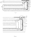
- the apparatus for identifying comprises an induction unit 1 and an identification unit 2, the set position of the induction unit 1 corresponding to the binding marker 3, and the induction unit 1 being capable of inducing a charge when the binding marker 3 is powered, the identification unit 2 being coupled to the induction unit 1, and used for receiving the charge induced by the induction unit 1, and identifying the binding marker 3 according to the induced charge.
- the binding marker 3 is formed employing a conductive material.
- the induction unit 1 induces a charge
- the identification unit 2 identifies the binding marker 3 according to the induced charge, thereby it may be achieved that the binding marker 3 may be normally identified even if it is covered with black ink, and in turn, the display appearance problem brought about by the design of the binding marker 3 opening in the reference (that is, the binding marker 3 is not shielded) is avoided, and meanwhile, it is avoided that a black ink material which may transmit light in a certain wavelength range is employed in the reference, thereby avoiding the problem of high process requirements brought about by employing such a black ink material.
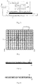
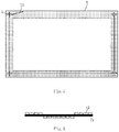
- the induction unit 1 comprises an insulating substrate 11 and a plurality of conductive sheets 12 set on the insulating substrate 11, and the plurality of conductive sheets 12 are spaced apart from each other and arranged in an array, and each of the conductive sheets 12 is coupled to a signal line (not shown in the figures) which is used for passing the charge induced on the conductive sheet 12 to the identification unit 2.
- the identification unit 2 comprises a reception module 21 and a conversion module 22, and the reception module 21 is coupled to the signal line, and used for receiving the charge induced by each of the conductive sheets 12.
- the conversion module 22 is coupled to the reception module 21, and used for converting the charge induced by each of the conductive sheets 12 into the voltage difference between each of the conductive sheets 12 and the binding marker 3, and determining the graphic of the binding marker 3 according to the voltage difference.
- the principle of induction of the binding marker 3 by the induction unit 1 employs the principle of capacitance induction, that is, when the binding marker 3 is powered, the conductive sheet 12 set corresponding to the binding marker 3 will induce a charge, and the conductive sheets 12 aligned with the binding marker 3 will induce charges with the same amount as but with the opposite polarity to the charges on the binding marker 3, whereas conductive sheets 12 non-aligned with the binding marker 3 will also induce charges with the opposite polarity to the charges on the binding marker 3, however, the amount of charges induced on the conductive sheets 12 non-aligned with the binding marker 3 is far less than the amount of charges on the binding marker 3, this causes that the voltage difference between the conductive sheets 12 aligned with the binding marker 3 and the binding marker 3 is larger than the voltage difference between the conductive sheets 12 non-aligned with the binding marker 3 and the binding marker 3, and the identification unit 2 identifies the voltage difference, and thereby may identify the graphic of the binding marker 3.
- the binding marker 3 is normally identified even if it is covered by black ink, such that the binding marker 3 may be covered by black ink which prevents light transmission, and in turn, the display appearance problem brought about by the design of the binding marker 3 opening in the reference (that is, the binding marker 3 is not shielded) is avoided, and meanwhile, it is avoided that a black ink material which may transmit light in a certain wavelength range is employed, thereby avoiding the problem of high process requirements brought about by employing such a black ink material.
- the conductive sheets 12 are located on the same side of the insulating substrate 11.
- the insulating substrate 11 may also be located in regions spaced apart from each other between the conductive sheets 12 (as shown in Fig. 6 ).
- the area of the orthographic projection of the induction unit 1 on a plane where the binding marker 3 is located is larger than the area of the binding marker 3.
- the induction unit 1 may be made to very easily correspond to the binding marker 3, thereby improving the alignment accuracy of the induction unit 1 and the binding marker 3, and in turn making it easier to identify the binding marker 3, and improving the efficiency of identifying the binding marker 3.
- the sizes and shapes of the plurality of conductive sheets 12 are identical, and the area of the binding marker 3 is n times the area of one of the conductive sheets 12, wherein n is an integer larger than 10.
- n is an integer larger than 10.
- the apparatus for identifying a binding marker further comprises a power unit 4 which is used for applying an electric signal to the binding marker 3. Therein, when it is needed to identify the binding marker 3, the power unit 4 applies the electric signal to the binding marker 3.
- the conductive sheets 12 and the binding marker 3 employ the same conductive material.
- the binding marker 3 is usually made employing the same material as the grid, and the conductive sheets 12 are also made employing the same material as the grid. As such, it is beneficial to the conductive sheets 12 inducting the powered binding marker 3.
- the conductive materials employed by the conductive sheets 12 and the binding marker 3 may also be different.
- the binding marker 3 is set on the light output side of the display panel 5, and the side of the binding marker 3 facing away from the display panel 5 is covered with a light shielding layer 6, and the induction unit is set facing the light shielding layer 6.
- the light shielding layer 6 employs black ink.
- the four sides of the display panel 5 are frameless, and the display panel 5 is adhered to the middle frame 71 of the backlight 7 by a double-sided adhesive.
- the color film substrate 51 of the display panel 5 is set close to the backlight 7, and the array substrate 52 is located on a side of the color film substrate 51 away from the backlight 7, causing the flexible printed circuit board 8 bound on the array substrate 52 to be wrapped inside the display structure constituted by the display panel 5 and the backlight 7. Since the metal wire of the peripheral wiring region of the array substrate 52 facing outwards is exposed and will reflect ambient light, the setting of the light shielding layer 6 may block the metal wire of the peripheral wiring region, thereby avoiding that the exposed metal wire reflects the ambient light and causing the appearance of the display panel 5 not to be affected.
- the binding marker 3 is located in the frame region of the display panel 5, there are comprised a plurality of binding markers 3, the plurality of binding markers 3 are electrically coupled to each other, and on one of the binding markers 3 is coupled a leading line 31 which is used for introducing an electric signal to the binding markers 3 to power the binding markers 3.
- a leading line 31 which is used for introducing an electric signal to the binding markers 3 to power the binding markers 3.
- the leading line 31 may be formed at the same time as the binding markers 3 in a one-time patterning process, the preparation process is simple and the preparation cost is low. In an actual power-up procedure, the electric signal may be applied to all the binding markers 3, as long as the power unit 4 is made to be in contact with the leading line 31.
- the display panel 5 comprises a control circuit (not shown in the figures) which is used for applying an electric signal to the binding marker 3. That is, the electric signal on the binding marker 3 may also be applied by the control circuit in the display panel 5. Namely, in an actual power-up procedure, the electric signal may be applied to all the binding markers 3, as long as the control circuit is made to be in contact with the leading line 31.
- This embodiment provides an apparatus for identifying a binding marker. Unlike embodiment One, as shown in Fig. 8 , one part of the conductive sheets 12 is located on one side of the insulating substrate 11, and the other part of the conductive sheets 12 is located on the other side of the insulating substrate 11.
- the beneficial effects of the embodiments One and Two are as follows.
- the induction unit may induce a charge
- the identification unit may identify the binding marker according to the induced charge, thereby it may be achieved that the binding marker may be normally identified even if it is covered by black ink, and in turn, the display appearance problem brought about by the design of the binding marker opening in the reference (that is, the binding marker is not shielded) is avoided, and meanwhile, it is avoided that a black ink material which may transmit light in a certain wavelength range is employed in the reference, thereby avoiding the problem of high process requirements brought about by employing such a black ink material.
- This embodiment provides a device for binding, comprising an apparatus for identifying a binding marker in embodiment One or Two.
- the device for binding is caused to be capable of normally identifying a binding marker even if it is covered by black ink, and thereby the device for binding is made to be capable of conducting normal alignment binding for a flexible printed circuit board even if the binding marker is covered by the black ink.
Landscapes
- Physics & Mathematics (AREA)
- Nonlinear Science (AREA)
- Chemical & Material Sciences (AREA)
- Crystallography & Structural Chemistry (AREA)
- General Physics & Mathematics (AREA)
- Optics & Photonics (AREA)
- Engineering & Computer Science (AREA)
- Manufacturing & Machinery (AREA)
- Mathematical Physics (AREA)
- Liquid Crystal (AREA)
- Structure Of Printed Boards (AREA)
- Control Of Indicators Other Than Cathode Ray Tubes (AREA)
Claims (13)
- Vorrichtung zum Identifizieren eines elektrisch leitenden Bindungsmarkers (3) eines Anzeigefeldes (5), umfassend eine Induktionseinheit (1) und eine Identifikationseinheit (2), wobei die Vorrichtung so ausgelegt ist, dass sie die Position der Induktionseinheit entsprechend der Position des Bindungsmarkers (3) festlegt, und die Induktionseinheit (1) zum Induzieren einer Ladung in der Induktionseinheit (1) imstande ist, wenn die Induktionseinheit (1) so positioniert ist, dass sie der Position des Bindungsmarkers (3) entspricht, und wenn der Bindungsmarker (3) durch ein elektrisches Signal mit Energie versorgt wird, wobei die Identifikationseinheit (2) mit der Induktionseinheit (1) gekoppelt und so ausgelegt ist, dass sie die von der Induktionseinheit (1) induzierte Ladung empfängt und den Bindungsmarker (3) gemäß der induzierten Ladung identifiziert,
dadurch gekennzeichnet, dass
die Induktionseinheit (1) ein Isolatorsubstrat (11) und eine Mehrzahl von leitenden Folien (12) umfasst, die auf dem Isolatorsubstrat (11) angeordnet ist, und die Mehrzahl von leitenden Folien (12) voneinander beabstandet und in einem Array angeordnet ist, und jede der leitenden Folien (12) mit einer Signalleitung gekoppelt ist, die zum Weitergeben der auf den leitenden Folien (12) induzierten Ladung zur Identifikationseinheit (2) ausgelegt ist. - Vorrichtung zum Identifizieren eines elektrisch leitenden Bindungsmarkers (3) nach Anspruch 1,
wobei die leitenden Folien (12) sich auf derselben Seite des Isolatorsubstrats (11) befinden. - Vorrichtung zum Identifizieren eines elektrisch leitenden Bindungsmarkers (3) nach Anspruch 1,
wobei das Isolatorsubstrat (11) sich in voneinander beabstandeten Regionen zwischen den leitenden Folien (12) befindet. - Vorrichtung zum Identifizieren eines elektrisch leitenden Bindungsmarkers (3) nach Anspruch 1,
wobei ein Teil der leitenden Folien (12) sich auf einer Seite des Isolatorsubstrats (11) befindet, und der andere Teil der leitenden Folien (12) sich auf der anderen Seite des Isolatorsubstrats (11) befindet. - Vorrichtung zum Identifizieren eines elektrisch leitenden Bindungsmarkers (3) nach einem der Ansprüche 1 bis 4, wobei die Vorrichtung derart ausgelegt ist, dass die Fläche der orthographischen Projektion der Induktionseinheit (1) auf einer Ebene, auf der sich der Bindungsmarker (3) befindet, größer als die Fläche des Bindungsmarkers (3) ist.
- Vorrichtung zum Identifizieren eines elektrisch leitenden Bindungsmarkers (3) nach einem der Ansprüche 1 bis 4, wobei sowohl die Größen als auch die Formen der Mehrzahl von leitenden Folien (12) identisch sind, und die Vorrichtung für Bindungsmarker (3) ausgelegt ist, wobei die Fläche des Bindungsmarkers (3) n-mal die Fläche einer der leitenden Folien (12) ist, wobei n eine ganze Zahl größer als 10 ist.
- Vorrichtung zum Identifizieren eines elektrisch leitenden Bindungsmarkers (3) nach Anspruch 1,wobei die Identifikationseinheit (2) ein Empfangsmodul (21) und ein Umwandlungsmodul (22) umfasst, und das Empfangsmodul (21) mit den Signalleitungen gekoppelt und zum Empfangen der durch jede der leitenden Folien (12) induzierten Ladung ausgelegt ist, unddas Umwandlungsmodul (22) mit dem Empfangsmodul (21) gekoppelt ist und verwendet wird, um die durch jede der leitenden Folien (12) induzierte Ladung in die Spannungsdifferenz zwischen jeder der leitenden Folien (12) und dem Bindungsmarker (3) umzuwandeln und die Grafik des Bindungsmarkers (3) gemäß der Spannungsdifferenz zu bestimmen.
- Vorrichtung zum Identifizieren eines elektrisch leitenden Bindungsmarkers (3) nach Anspruch 1,
wobei die Vorrichtung ferner eine Stromversorgungseinheit (4) umfasst, die zum Anlegen eines elektrischen Signals an den Bindungsmarker (3) ausgelegt ist. - Vorrichtung zum Identifizieren eines elektrisch leitenden Bindungsmarkers (3) nach Anspruch 1,
wobei die leitenden Folien (12) aus demselben leitenden Material wie das des leitenden Bindungsmarkers (3) gebildet sind. - Vorrichtung zum Identifizieren eines elektrisch leitenden Bindungsmarkers (3) nach Anspruch 1,
wobei die Vorrichtung so ausgelegt ist, dass sie die Induktionseinheit (1) so anordnet, dass sie einer Lichtabschirmungsschicht (6) zugewandt ist, vorausgesetzt, dass der Bindungsmarker (3) auf der Lichtausgabeseite des Anzeigefeldes (5) angeordnet ist und die Seite des Bindungsmarkers (3), die vom Anzeigefeld (5) abgewandt ist, mit der Lichtabschirmungseinheit (6) abgedeckt ist. - Vorrichtung zum Identifizieren eines elektrisch leitenden Bindungsmarkers (3) nach Anspruch 10, wobei die Vorrichtung zum Identifizieren eines elektrisch leitenden Bindungsmarkers (3) ausgelegt ist, der sich in der Rahmenregion des Anzeigefeldes (5) befindet, wobei das Anzeigefeld (5) eine Mehrzahl von Bindungsmarkern (3) umfasst, die Mehrzahl von Bindungsmarkern (3) untereinander elektrisch gekoppelt ist, und auf einem der Bindungsmarker (3) eine Signalleitung (31) gekoppelt ist, die zum Einführen eines elektrischen Signals in die Bindungsmarker (3) ausgelegt ist, um die Bindungsmarker (3) mit Energie zu versorgen.
- Vorrichtung zum Identifizieren eines elektrisch leitenden Bindungsmarkers (3) nach Anspruch 10, wobei die Vorrichtung zum Identifizieren eines elektrisch leitenden Bindungsmarkers eines Anzeigefeldes (5) ausgelegt ist, das eine Steuerschaltung umfasst, die zum Anlegen eines elektrischen Signals an den Bindungsmarker (3) ausgelegt ist.
- Bindevorrichtung, umfassend eine Vorrichtung zum Identifizieren eines elektrisch leitenden Bindungsmarkers (3) nach einem der Ansprüche 1 bis 12.
Applications Claiming Priority (2)
| Application Number | Priority Date | Filing Date | Title |
|---|---|---|---|
| CN201710081397.5A CN108427216B (zh) | 2017-02-15 | 2017-02-15 | 一种绑定标记识别装置和绑定设备 |
| PCT/CN2017/101199 WO2018149120A1 (zh) | 2017-02-15 | 2017-09-11 | 一种用于对绑定标记进行识别的装置和用于绑定的设备 |
Publications (3)
| Publication Number | Publication Date |
|---|---|
| EP3584629A1 EP3584629A1 (de) | 2019-12-25 |
| EP3584629A4 EP3584629A4 (de) | 2020-10-28 |
| EP3584629B1 true EP3584629B1 (de) | 2022-07-27 |
Family
ID=63155431
Family Applications (1)
| Application Number | Title | Priority Date | Filing Date |
|---|---|---|---|
| EP17847702.2A Not-in-force EP3584629B1 (de) | 2017-02-15 | 2017-09-11 | Vorrichtung zur identifizierung eines bindungsetiketts und vorrichtung zur bindung |
Country Status (4)
| Country | Link |
|---|---|
| US (1) | US10627660B2 (de) |
| EP (1) | EP3584629B1 (de) |
| CN (1) | CN108427216B (de) |
| WO (1) | WO2018149120A1 (de) |
Families Citing this family (4)
| Publication number | Priority date | Publication date | Assignee | Title |
|---|---|---|---|---|
| CN110174801B (zh) * | 2019-05-30 | 2024-03-26 | 武汉华星光电技术有限公司 | 显示模组 |
| CN113707019B (zh) * | 2021-08-30 | 2022-08-23 | 武汉华星光电半导体显示技术有限公司 | 显示装置及显示装置绑定区的对位标记识别方法 |
| CN114399957B (zh) * | 2022-03-04 | 2023-07-04 | 武汉华星光电半导体显示技术有限公司 | 显示面板及显示面板的制作方法、移动终端 |
| CN116978286B (zh) * | 2023-08-15 | 2026-02-27 | 京东方科技集团股份有限公司 | 显示模组及其制作方法、显示装置 |
Family Cites Families (20)
| Publication number | Priority date | Publication date | Assignee | Title |
|---|---|---|---|---|
| JPH0996712A (ja) * | 1995-09-29 | 1997-04-08 | Sony Corp | カラーフィルタの製造方法 |
| KR20070080426A (ko) * | 2006-02-07 | 2007-08-10 | 엘지.필립스 엘시디 주식회사 | 액정표시장치 및 그 제조방법 |
| WO2008111214A1 (ja) * | 2007-03-15 | 2008-09-18 | Fujitsu Limited | 表示パネル、積層型表示素子及びその製造方法 |
| KR100814097B1 (ko) * | 2007-06-25 | 2008-03-14 | 일신하이텍 주식회사 | 비접촉 급전장치를 포함하는 엘시디 에이징 시스템 |
| CN101403829A (zh) | 2008-11-10 | 2009-04-08 | 友达光电(苏州)有限公司 | 对位检测方法和对位检测装置 |
| CN101598878B (zh) * | 2009-06-25 | 2011-04-13 | 友达光电股份有限公司 | 有源元件阵列基板与显示面板 |
| WO2011043103A1 (ja) * | 2009-10-07 | 2011-04-14 | シャープ株式会社 | 液晶パネルおよび液晶表示装置 |
| US20130321719A1 (en) * | 2011-02-22 | 2013-12-05 | Sharp Kabushiki Kaisha | Electronic device and method for manufacturing same |
| CN102749771B (zh) * | 2012-04-06 | 2015-02-04 | 信利工业(汕尾)有限公司 | 一种集成nfc天线的薄膜晶体管显示器 |
| CN102608797A (zh) | 2012-04-09 | 2012-07-25 | 友达光电股份有限公司 | 一种用于液晶显示设备组装时的对准方法 |
| CN102929012B (zh) * | 2012-10-29 | 2015-02-18 | 京东方科技集团股份有限公司 | 显示装置 |
| US9025119B2 (en) * | 2013-05-14 | 2015-05-05 | Shenzhen China Star Optoelectronics Technology Co., Ltd. | LCD module and liquid crystal panel |
| CN103677427A (zh) * | 2013-12-26 | 2014-03-26 | 京东方科技集团股份有限公司 | 触控显示装置驱动方法及触控显示装置 |
| KR20160010774A (ko) * | 2014-07-18 | 2016-01-28 | 삼성디스플레이 주식회사 | 표시장치 |
| CN104516163B (zh) * | 2015-01-15 | 2018-02-16 | 京东方科技集团股份有限公司 | 一种显示基板和显示装置 |
| CN106155398A (zh) * | 2015-04-23 | 2016-11-23 | 南昌欧菲光科技有限公司 | 触控装置及柔性电路板绑定定位方法 |
| CN104965359B (zh) * | 2015-07-20 | 2017-12-29 | 深圳市华星光电技术有限公司 | 多重稳态液晶显示面板 |
| CN205375441U (zh) * | 2015-12-31 | 2016-07-06 | 南京点触智能科技有限公司 | 一种半透镜面的电容式触控屏 |
| US9964793B2 (en) * | 2016-02-23 | 2018-05-08 | Microsoft Technology Licensing, Llc | Dissipation layer in a display device |
| CN105892160A (zh) * | 2016-05-27 | 2016-08-24 | 厦门天马微电子有限公司 | 液晶显示面板 |
-
2017
- 2017-02-15 CN CN201710081397.5A patent/CN108427216B/zh not_active Expired - Fee Related
- 2017-09-11 WO PCT/CN2017/101199 patent/WO2018149120A1/zh not_active Ceased
- 2017-09-11 EP EP17847702.2A patent/EP3584629B1/de not_active Not-in-force
- 2017-09-11 US US15/759,167 patent/US10627660B2/en not_active Expired - Fee Related
Also Published As
| Publication number | Publication date |
|---|---|
| WO2018149120A1 (zh) | 2018-08-23 |
| CN108427216A (zh) | 2018-08-21 |
| EP3584629A4 (de) | 2020-10-28 |
| EP3584629A1 (de) | 2019-12-25 |
| US20190049772A1 (en) | 2019-02-14 |
| CN108427216B (zh) | 2020-11-17 |
| US10627660B2 (en) | 2020-04-21 |
Similar Documents
| Publication | Publication Date | Title |
|---|---|---|
| TWI497154B (zh) | 光電裝置 | |
| AU2011233904B2 (en) | Touch screen panel | |
| CN217718922U (zh) | 显示装置 | |
| CN218447089U (zh) | 显示装置 | |
| US9696768B2 (en) | Touch type organic light emitting diode display device | |
| US10627660B2 (en) | Apparatus for identifying a binding marker and device for binding | |
| WO2011030773A1 (ja) | 狭額縁タッチ入力シートとその製造方法および狭額縁タッチ入力シートに用いる導電性シート | |
| CN113411939B (zh) | 一种显示模组 | |
| US9954012B2 (en) | Display device | |
| US9395759B2 (en) | Protective window for display device and display device including the same | |
| US20120050190A1 (en) | Display apparatus | |
| CN103383503B (zh) | 彩色滤光片基板及触控显示装置 | |
| CN103345316A (zh) | 具有触控功能的电子装置 | |
| CN110018586A (zh) | 一种显示面板及其对盒方法、显示装置、对盒装置 | |
| US10725232B2 (en) | Backlight device and liquid crystal display device comprising the same | |
| KR102448501B1 (ko) | 표시 장치 | |
| JP4838643B2 (ja) | 入力装置付表示装置 | |
| CN106094301A (zh) | 压力触控式液晶显示装置及其制作方法 | |
| CN203120284U (zh) | 柔性线路板及液晶显示装置 | |
| CN203102236U (zh) | 单片式无金属痕电容式触控玻璃 | |
| CN222190174U (zh) | 显示装置 | |
| JP2008009553A (ja) | 電極基板 | |
| US9351401B2 (en) | Display panel and display device | |
| JP2007025626A (ja) | 電気光学装置及び電子機器 | |
| WO2011001828A1 (ja) | 座標入力装置とそれを備えた表示装置及び電子機器 |
Legal Events
| Date | Code | Title | Description |
|---|---|---|---|
| STAA | Information on the status of an ep patent application or granted ep patent |
Free format text: STATUS: UNKNOWN |
|
| STAA | Information on the status of an ep patent application or granted ep patent |
Free format text: STATUS: THE INTERNATIONAL PUBLICATION HAS BEEN MADE |
|
| PUAI | Public reference made under article 153(3) epc to a published international application that has entered the european phase |
Free format text: ORIGINAL CODE: 0009012 |
|
| STAA | Information on the status of an ep patent application or granted ep patent |
Free format text: STATUS: REQUEST FOR EXAMINATION WAS MADE |
|
| 17P | Request for examination filed |
Effective date: 20180312 |
|
| AK | Designated contracting states |
Kind code of ref document: A1 Designated state(s): AL AT BE BG CH CY CZ DE DK EE ES FI FR GB GR HR HU IE IS IT LI LT LU LV MC MK MT NL NO PL PT RO RS SE SI SK SM TR |
|
| AX | Request for extension of the european patent |
Extension state: BA ME |
|
| DAV | Request for validation of the european patent (deleted) | ||
| DAX | Request for extension of the european patent (deleted) | ||
| A4 | Supplementary search report drawn up and despatched |
Effective date: 20200930 |
|
| RIC1 | Information provided on ipc code assigned before grant |
Ipc: G02F 1/13 20060101AFI20200924BHEP |
|
| GRAP | Despatch of communication of intention to grant a patent |
Free format text: ORIGINAL CODE: EPIDOSNIGR1 |
|
| STAA | Information on the status of an ep patent application or granted ep patent |
Free format text: STATUS: GRANT OF PATENT IS INTENDED |
|
| INTG | Intention to grant announced |
Effective date: 20220211 |
|
| GRAS | Grant fee paid |
Free format text: ORIGINAL CODE: EPIDOSNIGR3 |
|
| GRAA | (expected) grant |
Free format text: ORIGINAL CODE: 0009210 |
|
| STAA | Information on the status of an ep patent application or granted ep patent |
Free format text: STATUS: THE PATENT HAS BEEN GRANTED |
|
| AK | Designated contracting states |
Kind code of ref document: B1 Designated state(s): AL AT BE BG CH CY CZ DE DK EE ES FI FR GB GR HR HU IE IS IT LI LT LU LV MC MK MT NL NO PL PT RO RS SE SI SK SM TR |
|
| REG | Reference to a national code |
Ref country code: CH Ref legal event code: EP |
|
| REG | Reference to a national code |
Ref country code: AT Ref legal event code: REF Ref document number: 1507448 Country of ref document: AT Kind code of ref document: T Effective date: 20220815 |
|
| REG | Reference to a national code |
Ref country code: DE Ref legal event code: R096 Ref document number: 602017059991 Country of ref document: DE |
|
| REG | Reference to a national code |
Ref country code: IE Ref legal event code: FG4D |
|
| REG | Reference to a national code |
Ref country code: LT Ref legal event code: MG9D |
|
| REG | Reference to a national code |
Ref country code: NL Ref legal event code: MP Effective date: 20220727 |
|
| PG25 | Lapsed in a contracting state [announced via postgrant information from national office to epo] |
Ref country code: SE Free format text: LAPSE BECAUSE OF FAILURE TO SUBMIT A TRANSLATION OF THE DESCRIPTION OR TO PAY THE FEE WITHIN THE PRESCRIBED TIME-LIMIT Effective date: 20220727 Ref country code: RS Free format text: LAPSE BECAUSE OF FAILURE TO SUBMIT A TRANSLATION OF THE DESCRIPTION OR TO PAY THE FEE WITHIN THE PRESCRIBED TIME-LIMIT Effective date: 20220727 Ref country code: PT Free format text: LAPSE BECAUSE OF FAILURE TO SUBMIT A TRANSLATION OF THE DESCRIPTION OR TO PAY THE FEE WITHIN THE PRESCRIBED TIME-LIMIT Effective date: 20221128 Ref country code: NO Free format text: LAPSE BECAUSE OF FAILURE TO SUBMIT A TRANSLATION OF THE DESCRIPTION OR TO PAY THE FEE WITHIN THE PRESCRIBED TIME-LIMIT Effective date: 20221027 Ref country code: NL Free format text: LAPSE BECAUSE OF FAILURE TO SUBMIT A TRANSLATION OF THE DESCRIPTION OR TO PAY THE FEE WITHIN THE PRESCRIBED TIME-LIMIT Effective date: 20220727 Ref country code: LV Free format text: LAPSE BECAUSE OF FAILURE TO SUBMIT A TRANSLATION OF THE DESCRIPTION OR TO PAY THE FEE WITHIN THE PRESCRIBED TIME-LIMIT Effective date: 20220727 Ref country code: LT Free format text: LAPSE BECAUSE OF FAILURE TO SUBMIT A TRANSLATION OF THE DESCRIPTION OR TO PAY THE FEE WITHIN THE PRESCRIBED TIME-LIMIT Effective date: 20220727 Ref country code: FI Free format text: LAPSE BECAUSE OF FAILURE TO SUBMIT A TRANSLATION OF THE DESCRIPTION OR TO PAY THE FEE WITHIN THE PRESCRIBED TIME-LIMIT Effective date: 20220727 Ref country code: ES Free format text: LAPSE BECAUSE OF FAILURE TO SUBMIT A TRANSLATION OF THE DESCRIPTION OR TO PAY THE FEE WITHIN THE PRESCRIBED TIME-LIMIT Effective date: 20220727 |
|
| REG | Reference to a national code |
Ref country code: AT Ref legal event code: MK05 Ref document number: 1507448 Country of ref document: AT Kind code of ref document: T Effective date: 20220727 |
|
| PG25 | Lapsed in a contracting state [announced via postgrant information from national office to epo] |
Ref country code: PL Free format text: LAPSE BECAUSE OF FAILURE TO SUBMIT A TRANSLATION OF THE DESCRIPTION OR TO PAY THE FEE WITHIN THE PRESCRIBED TIME-LIMIT Effective date: 20220727 Ref country code: IS Free format text: LAPSE BECAUSE OF FAILURE TO SUBMIT A TRANSLATION OF THE DESCRIPTION OR TO PAY THE FEE WITHIN THE PRESCRIBED TIME-LIMIT Effective date: 20221127 Ref country code: HR Free format text: LAPSE BECAUSE OF FAILURE TO SUBMIT A TRANSLATION OF THE DESCRIPTION OR TO PAY THE FEE WITHIN THE PRESCRIBED TIME-LIMIT Effective date: 20220727 Ref country code: GR Free format text: LAPSE BECAUSE OF FAILURE TO SUBMIT A TRANSLATION OF THE DESCRIPTION OR TO PAY THE FEE WITHIN THE PRESCRIBED TIME-LIMIT Effective date: 20221028 |
|
| PG25 | Lapsed in a contracting state [announced via postgrant information from national office to epo] |
Ref country code: SM Free format text: LAPSE BECAUSE OF FAILURE TO SUBMIT A TRANSLATION OF THE DESCRIPTION OR TO PAY THE FEE WITHIN THE PRESCRIBED TIME-LIMIT Effective date: 20220727 Ref country code: RO Free format text: LAPSE BECAUSE OF FAILURE TO SUBMIT A TRANSLATION OF THE DESCRIPTION OR TO PAY THE FEE WITHIN THE PRESCRIBED TIME-LIMIT Effective date: 20220727 Ref country code: MC Free format text: LAPSE BECAUSE OF FAILURE TO SUBMIT A TRANSLATION OF THE DESCRIPTION OR TO PAY THE FEE WITHIN THE PRESCRIBED TIME-LIMIT Effective date: 20220727 Ref country code: DK Free format text: LAPSE BECAUSE OF FAILURE TO SUBMIT A TRANSLATION OF THE DESCRIPTION OR TO PAY THE FEE WITHIN THE PRESCRIBED TIME-LIMIT Effective date: 20220727 Ref country code: CZ Free format text: LAPSE BECAUSE OF FAILURE TO SUBMIT A TRANSLATION OF THE DESCRIPTION OR TO PAY THE FEE WITHIN THE PRESCRIBED TIME-LIMIT Effective date: 20220727 Ref country code: AT Free format text: LAPSE BECAUSE OF FAILURE TO SUBMIT A TRANSLATION OF THE DESCRIPTION OR TO PAY THE FEE WITHIN THE PRESCRIBED TIME-LIMIT Effective date: 20220727 |
|
| REG | Reference to a national code |
Ref country code: CH Ref legal event code: PL |
|
| REG | Reference to a national code |
Ref country code: DE Ref legal event code: R097 Ref document number: 602017059991 Country of ref document: DE |
|
| REG | Reference to a national code |
Ref country code: BE Ref legal event code: MM Effective date: 20220930 |
|
| PG25 | Lapsed in a contracting state [announced via postgrant information from national office to epo] |
Ref country code: SK Free format text: LAPSE BECAUSE OF FAILURE TO SUBMIT A TRANSLATION OF THE DESCRIPTION OR TO PAY THE FEE WITHIN THE PRESCRIBED TIME-LIMIT Effective date: 20220727 Ref country code: EE Free format text: LAPSE BECAUSE OF FAILURE TO SUBMIT A TRANSLATION OF THE DESCRIPTION OR TO PAY THE FEE WITHIN THE PRESCRIBED TIME-LIMIT Effective date: 20220727 |
|
| PLBE | No opposition filed within time limit |
Free format text: ORIGINAL CODE: 0009261 |
|
| STAA | Information on the status of an ep patent application or granted ep patent |
Free format text: STATUS: NO OPPOSITION FILED WITHIN TIME LIMIT |
|
| GBPC | Gb: european patent ceased through non-payment of renewal fee |
Effective date: 20221027 |
|
| PG25 | Lapsed in a contracting state [announced via postgrant information from national office to epo] |
Ref country code: LU Free format text: LAPSE BECAUSE OF NON-PAYMENT OF DUE FEES Effective date: 20220911 Ref country code: AL Free format text: LAPSE BECAUSE OF FAILURE TO SUBMIT A TRANSLATION OF THE DESCRIPTION OR TO PAY THE FEE WITHIN THE PRESCRIBED TIME-LIMIT Effective date: 20220727 |
|
| 26N | No opposition filed |
Effective date: 20230502 |
|
| PG25 | Lapsed in a contracting state [announced via postgrant information from national office to epo] |
Ref country code: IE Free format text: LAPSE BECAUSE OF NON-PAYMENT OF DUE FEES Effective date: 20220911 Ref country code: FR Free format text: LAPSE BECAUSE OF NON-PAYMENT OF DUE FEES Effective date: 20220927 Ref country code: CH Free format text: LAPSE BECAUSE OF NON-PAYMENT OF DUE FEES Effective date: 20220930 Ref country code: LI Free format text: LAPSE BECAUSE OF NON-PAYMENT OF DUE FEES Effective date: 20220930 |
|
| PG25 | Lapsed in a contracting state [announced via postgrant information from national office to epo] |
Ref country code: SI Free format text: LAPSE BECAUSE OF FAILURE TO SUBMIT A TRANSLATION OF THE DESCRIPTION OR TO PAY THE FEE WITHIN THE PRESCRIBED TIME-LIMIT Effective date: 20220727 |
|
| PG25 | Lapsed in a contracting state [announced via postgrant information from national office to epo] |
Ref country code: BE Free format text: LAPSE BECAUSE OF NON-PAYMENT OF DUE FEES Effective date: 20220930 |
|
| PG25 | Lapsed in a contracting state [announced via postgrant information from national office to epo] |
Ref country code: GB Free format text: LAPSE BECAUSE OF NON-PAYMENT OF DUE FEES Effective date: 20221027 |
|
| PGFP | Annual fee paid to national office [announced via postgrant information from national office to epo] |
Ref country code: DE Payment date: 20230920 Year of fee payment: 7 |
|
| PG25 | Lapsed in a contracting state [announced via postgrant information from national office to epo] |
Ref country code: HU Free format text: LAPSE BECAUSE OF FAILURE TO SUBMIT A TRANSLATION OF THE DESCRIPTION OR TO PAY THE FEE WITHIN THE PRESCRIBED TIME-LIMIT; INVALID AB INITIO Effective date: 20170911 |
|
| PG25 | Lapsed in a contracting state [announced via postgrant information from national office to epo] |
Ref country code: CY Free format text: LAPSE BECAUSE OF FAILURE TO SUBMIT A TRANSLATION OF THE DESCRIPTION OR TO PAY THE FEE WITHIN THE PRESCRIBED TIME-LIMIT Effective date: 20220727 |
|
| PG25 | Lapsed in a contracting state [announced via postgrant information from national office to epo] |
Ref country code: MK Free format text: LAPSE BECAUSE OF FAILURE TO SUBMIT A TRANSLATION OF THE DESCRIPTION OR TO PAY THE FEE WITHIN THE PRESCRIBED TIME-LIMIT Effective date: 20220727 Ref country code: IT Free format text: LAPSE BECAUSE OF FAILURE TO SUBMIT A TRANSLATION OF THE DESCRIPTION OR TO PAY THE FEE WITHIN THE PRESCRIBED TIME-LIMIT Effective date: 20220727 |
|
| PG25 | Lapsed in a contracting state [announced via postgrant information from national office to epo] |
Ref country code: BG Free format text: LAPSE BECAUSE OF FAILURE TO SUBMIT A TRANSLATION OF THE DESCRIPTION OR TO PAY THE FEE WITHIN THE PRESCRIBED TIME-LIMIT Effective date: 20220727 |
|
| PG25 | Lapsed in a contracting state [announced via postgrant information from national office to epo] |
Ref country code: MT Free format text: LAPSE BECAUSE OF FAILURE TO SUBMIT A TRANSLATION OF THE DESCRIPTION OR TO PAY THE FEE WITHIN THE PRESCRIBED TIME-LIMIT Effective date: 20220727 |
|
| REG | Reference to a national code |
Ref country code: DE Ref legal event code: R119 Ref document number: 602017059991 Country of ref document: DE |
|
| PG25 | Lapsed in a contracting state [announced via postgrant information from national office to epo] |
Ref country code: DE Free format text: LAPSE BECAUSE OF NON-PAYMENT OF DUE FEES Effective date: 20250401 |
|
| PG25 | Lapsed in a contracting state [announced via postgrant information from national office to epo] |
Ref country code: TR Free format text: LAPSE BECAUSE OF FAILURE TO SUBMIT A TRANSLATION OF THE DESCRIPTION OR TO PAY THE FEE WITHIN THE PRESCRIBED TIME-LIMIT Effective date: 20220727 |