EP3576151A1 - Halbleiterbauelement, verfahren zur herstellung davon, festkörperbildaufnahmeelement und elektronische vorrichtung - Google Patents
Halbleiterbauelement, verfahren zur herstellung davon, festkörperbildaufnahmeelement und elektronische vorrichtung Download PDFInfo
- Publication number
- EP3576151A1 EP3576151A1 EP18744431.0A EP18744431A EP3576151A1 EP 3576151 A1 EP3576151 A1 EP 3576151A1 EP 18744431 A EP18744431 A EP 18744431A EP 3576151 A1 EP3576151 A1 EP 3576151A1
- Authority
- EP
- European Patent Office
- Prior art keywords
- semiconductor substrate
- hole
- insulating film
- deposited
- electrodes
- Prior art date
- Legal status (The legal status is an assumption and is not a legal conclusion. Google has not performed a legal analysis and makes no representation as to the accuracy of the status listed.)
- Granted
Links
Images







Classifications
-
- H—ELECTRICITY
- H10—SEMICONDUCTOR DEVICES; ELECTRIC SOLID-STATE DEVICES NOT OTHERWISE PROVIDED FOR
- H10F—INORGANIC SEMICONDUCTOR DEVICES SENSITIVE TO INFRARED RADIATION, LIGHT, ELECTROMAGNETIC RADIATION OF SHORTER WAVELENGTH OR CORPUSCULAR RADIATION
- H10F39/00—Integrated devices, or assemblies of multiple devices, comprising at least one element covered by group H10F30/00, e.g. radiation detectors comprising photodiode arrays
- H10F39/10—Integrated devices
- H10F39/12—Image sensors
-
- H—ELECTRICITY
- H04—ELECTRIC COMMUNICATION TECHNIQUE
- H04N—PICTORIAL COMMUNICATION, e.g. TELEVISION
- H04N25/00—Circuitry of solid-state image sensors [SSIS]; Control thereof
- H04N25/70—SSIS architectures; Circuits associated therewith
-
- H—ELECTRICITY
- H10—SEMICONDUCTOR DEVICES; ELECTRIC SOLID-STATE DEVICES NOT OTHERWISE PROVIDED FOR
- H10D—INORGANIC ELECTRIC SEMICONDUCTOR DEVICES
- H10D84/00—Integrated devices formed in or on semiconductor substrates that comprise only semiconducting layers, e.g. on Si wafers or on GaAs-on-Si wafers
-
- H—ELECTRICITY
- H10—SEMICONDUCTOR DEVICES; ELECTRIC SOLID-STATE DEVICES NOT OTHERWISE PROVIDED FOR
- H10D—INORGANIC ELECTRIC SEMICONDUCTOR DEVICES
- H10D84/00—Integrated devices formed in or on semiconductor substrates that comprise only semiconducting layers, e.g. on Si wafers or on GaAs-on-Si wafers
- H10D84/01—Manufacture or treatment
- H10D84/02—Manufacture or treatment characterised by using material-based technologies
- H10D84/03—Manufacture or treatment characterised by using material-based technologies using Group IV technology, e.g. silicon technology or silicon-carbide [SiC] technology
- H10D84/038—Manufacture or treatment characterised by using material-based technologies using Group IV technology, e.g. silicon technology or silicon-carbide [SiC] technology using silicon technology, e.g. SiGe
-
- H—ELECTRICITY
- H10—SEMICONDUCTOR DEVICES; ELECTRIC SOLID-STATE DEVICES NOT OTHERWISE PROVIDED FOR
- H10D—INORGANIC ELECTRIC SEMICONDUCTOR DEVICES
- H10D89/00—Aspects of integrated devices not covered by groups H10D84/00 - H10D88/00
- H10D89/60—Integrated devices comprising arrangements for electrical or thermal protection, e.g. protection circuits against electrostatic discharge [ESD]
- H10D89/601—Integrated devices comprising arrangements for electrical or thermal protection, e.g. protection circuits against electrostatic discharge [ESD] for devices having insulated gate electrodes, e.g. for IGFETs or IGBTs
- H10D89/611—Integrated devices comprising arrangements for electrical or thermal protection, e.g. protection circuits against electrostatic discharge [ESD] for devices having insulated gate electrodes, e.g. for IGFETs or IGBTs using diodes as protective elements
-
- H—ELECTRICITY
- H10—SEMICONDUCTOR DEVICES; ELECTRIC SOLID-STATE DEVICES NOT OTHERWISE PROVIDED FOR
- H10D—INORGANIC ELECTRIC SEMICONDUCTOR DEVICES
- H10D89/00—Aspects of integrated devices not covered by groups H10D84/00 - H10D88/00
- H10D89/60—Integrated devices comprising arrangements for electrical or thermal protection, e.g. protection circuits against electrostatic discharge [ESD]
- H10D89/601—Integrated devices comprising arrangements for electrical or thermal protection, e.g. protection circuits against electrostatic discharge [ESD] for devices having insulated gate electrodes, e.g. for IGFETs or IGBTs
- H10D89/931—Integrated devices comprising arrangements for electrical or thermal protection, e.g. protection circuits against electrostatic discharge [ESD] for devices having insulated gate electrodes, e.g. for IGFETs or IGBTs characterised by the dispositions of the protective arrangements
-
- H—ELECTRICITY
- H10—SEMICONDUCTOR DEVICES; ELECTRIC SOLID-STATE DEVICES NOT OTHERWISE PROVIDED FOR
- H10F—INORGANIC SEMICONDUCTOR DEVICES SENSITIVE TO INFRARED RADIATION, LIGHT, ELECTROMAGNETIC RADIATION OF SHORTER WAVELENGTH OR CORPUSCULAR RADIATION
- H10F39/00—Integrated devices, or assemblies of multiple devices, comprising at least one element covered by group H10F30/00, e.g. radiation detectors comprising photodiode arrays
- H10F39/011—Manufacture or treatment of image sensors covered by group H10F39/12
- H10F39/018—Manufacture or treatment of image sensors covered by group H10F39/12 of hybrid image sensors
-
- H—ELECTRICITY
- H10—SEMICONDUCTOR DEVICES; ELECTRIC SOLID-STATE DEVICES NOT OTHERWISE PROVIDED FOR
- H10F—INORGANIC SEMICONDUCTOR DEVICES SENSITIVE TO INFRARED RADIATION, LIGHT, ELECTROMAGNETIC RADIATION OF SHORTER WAVELENGTH OR CORPUSCULAR RADIATION
- H10F39/00—Integrated devices, or assemblies of multiple devices, comprising at least one element covered by group H10F30/00, e.g. radiation detectors comprising photodiode arrays
- H10F39/80—Constructional details of image sensors
- H10F39/809—Constructional details of image sensors of hybrid image sensors
-
- H—ELECTRICITY
- H10—SEMICONDUCTOR DEVICES; ELECTRIC SOLID-STATE DEVICES NOT OTHERWISE PROVIDED FOR
- H10F—INORGANIC SEMICONDUCTOR DEVICES SENSITIVE TO INFRARED RADIATION, LIGHT, ELECTROMAGNETIC RADIATION OF SHORTER WAVELENGTH OR CORPUSCULAR RADIATION
- H10F39/00—Integrated devices, or assemblies of multiple devices, comprising at least one element covered by group H10F30/00, e.g. radiation detectors comprising photodiode arrays
- H10F39/80—Constructional details of image sensors
- H10F39/811—Interconnections
-
- H—ELECTRICITY
- H10—SEMICONDUCTOR DEVICES; ELECTRIC SOLID-STATE DEVICES NOT OTHERWISE PROVIDED FOR
- H10P—GENERIC PROCESSES OR APPARATUS FOR THE MANUFACTURE OR TREATMENT OF DEVICES COVERED BY CLASS H10
- H10P14/00—Formation of materials, e.g. in the shape of layers or pillars
- H10P14/40—Formation of materials, e.g. in the shape of layers or pillars of conductive or resistive materials
-
- H—ELECTRICITY
- H10—SEMICONDUCTOR DEVICES; ELECTRIC SOLID-STATE DEVICES NOT OTHERWISE PROVIDED FOR
- H10W—GENERIC PACKAGES, INTERCONNECTIONS, CONNECTORS OR OTHER CONSTRUCTIONAL DETAILS OF DEVICES COVERED BY CLASS H10
- H10W20/00—Interconnections in chips, wafers or substrates
- H10W20/01—Manufacture or treatment
-
- H—ELECTRICITY
- H10—SEMICONDUCTOR DEVICES; ELECTRIC SOLID-STATE DEVICES NOT OTHERWISE PROVIDED FOR
- H10W—GENERIC PACKAGES, INTERCONNECTIONS, CONNECTORS OR OTHER CONSTRUCTIONAL DETAILS OF DEVICES COVERED BY CLASS H10
- H10W20/00—Interconnections in chips, wafers or substrates
- H10W20/01—Manufacture or treatment
- H10W20/021—Manufacture or treatment of interconnections within wafers or substrates
- H10W20/023—Manufacture or treatment of interconnections within wafers or substrates the interconnections being through-semiconductor vias
-
- H—ELECTRICITY
- H10—SEMICONDUCTOR DEVICES; ELECTRIC SOLID-STATE DEVICES NOT OTHERWISE PROVIDED FOR
- H10W—GENERIC PACKAGES, INTERCONNECTIONS, CONNECTORS OR OTHER CONSTRUCTIONAL DETAILS OF DEVICES COVERED BY CLASS H10
- H10W20/00—Interconnections in chips, wafers or substrates
- H10W20/01—Manufacture or treatment
- H10W20/021—Manufacture or treatment of interconnections within wafers or substrates
- H10W20/023—Manufacture or treatment of interconnections within wafers or substrates the interconnections being through-semiconductor vias
- H10W20/0234—Manufacture or treatment of interconnections within wafers or substrates the interconnections being through-semiconductor vias comprising etching via holes that stop on pads or on electrodes
-
- H—ELECTRICITY
- H10—SEMICONDUCTOR DEVICES; ELECTRIC SOLID-STATE DEVICES NOT OTHERWISE PROVIDED FOR
- H10W—GENERIC PACKAGES, INTERCONNECTIONS, CONNECTORS OR OTHER CONSTRUCTIONAL DETAILS OF DEVICES COVERED BY CLASS H10
- H10W20/00—Interconnections in chips, wafers or substrates
- H10W20/01—Manufacture or treatment
- H10W20/021—Manufacture or treatment of interconnections within wafers or substrates
- H10W20/023—Manufacture or treatment of interconnections within wafers or substrates the interconnections being through-semiconductor vias
- H10W20/0242—Manufacture or treatment of interconnections within wafers or substrates the interconnections being through-semiconductor vias comprising etching via holes from the back sides of the chips, wafers or substrates
-
- H—ELECTRICITY
- H10—SEMICONDUCTOR DEVICES; ELECTRIC SOLID-STATE DEVICES NOT OTHERWISE PROVIDED FOR
- H10W—GENERIC PACKAGES, INTERCONNECTIONS, CONNECTORS OR OTHER CONSTRUCTIONAL DETAILS OF DEVICES COVERED BY CLASS H10
- H10W20/00—Interconnections in chips, wafers or substrates
- H10W20/20—Interconnections within wafers or substrates, e.g. through-silicon vias [TSV]
-
- H—ELECTRICITY
- H10—SEMICONDUCTOR DEVICES; ELECTRIC SOLID-STATE DEVICES NOT OTHERWISE PROVIDED FOR
- H10W—GENERIC PACKAGES, INTERCONNECTIONS, CONNECTORS OR OTHER CONSTRUCTIONAL DETAILS OF DEVICES COVERED BY CLASS H10
- H10W20/00—Interconnections in chips, wafers or substrates
- H10W20/40—Interconnections external to wafers or substrates, e.g. back-end-of-line [BEOL] metallisations or vias connecting to gate electrodes
-
- H—ELECTRICITY
- H10—SEMICONDUCTOR DEVICES; ELECTRIC SOLID-STATE DEVICES NOT OTHERWISE PROVIDED FOR
- H10W—GENERIC PACKAGES, INTERCONNECTIONS, CONNECTORS OR OTHER CONSTRUCTIONAL DETAILS OF DEVICES COVERED BY CLASS H10
- H10W90/00—Package configurations
-
- H—ELECTRICITY
- H10—SEMICONDUCTOR DEVICES; ELECTRIC SOLID-STATE DEVICES NOT OTHERWISE PROVIDED FOR
- H10D—INORGANIC ELECTRIC SEMICONDUCTOR DEVICES
- H10D88/00—Three-dimensional [3D] integrated devices
-
- H—ELECTRICITY
- H10—SEMICONDUCTOR DEVICES; ELECTRIC SOLID-STATE DEVICES NOT OTHERWISE PROVIDED FOR
- H10D—INORGANIC ELECTRIC SEMICONDUCTOR DEVICES
- H10D88/00—Three-dimensional [3D] integrated devices
- H10D88/01—Manufacture or treatment
Definitions
- the present disclosure relates to a semiconductor device and a manufacturing method therefor, a solid-state imaging element and electronic equipment, and particularly relates to a semiconductor device and a manufacturing method therefor, a solid-state imaging element and electronic equipment suitable for use in the case where semiconductor substrates stacked on each other are electrically connected to each other by a through electrode.
- an amplification type solid-state imaging element represented by a MOS type image sensor such as a CMOS (Complementary Metal Oxide Semiconductor), a multilayer stacked memory, and so forth have been known (for example, refer to PTL 1).
- MOS type image sensor such as a CMOS (Complementary Metal Oxide Semiconductor), a multilayer stacked memory, and so forth have been known (for example, refer to PTL 1).
- FIG. 1 is a sectional view depicting an example of a related-art configuration of electronic equipment configured by stacking a plurality of semiconductor substrates.
- the electronic equipment is configured such that a first semiconductor substrate 11 is stacked on a second semiconductor substrate 12 and a through electrode 13 is formed by filling a through-hole (penetrating hole) extending through the two semiconductor substrates with an electrode material (a metal material such as, for example, Cu) to electrically connect a wiring line of the first semiconductor substrate 11 of the upper layer and a wiring line of the second semiconductor substrate 12 of the lower layer with each other.
- an electrode material a metal material such as, for example, Cu
- FIG. 2 is an enlarged view depicting a cross section of the first semiconductor substrate 11 in which the through electrode 13 is formed.
- the through electrode 13 is formed in the first semiconductor substrate 11 (hereinafter referred to also as an Si substrate 11) represented by an Si substrate
- Si substrate 11 an Si substrate
- an insulation resistance of the side wall insulating film 23 increases as a thickness thereof increases, there is a limitation from the point of view of a throughput or fine processing, and it is desirable that the side wall insulating film 23 is controlled to an appropriate thickness.
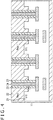
- a cause of the breakdown phenomenon of the side wall insulating film 23 is described in detail with reference to FIGS. 3 and 4 .
- the breakdown phenomenon of the side wall insulating film 23 arises from injection of a charge arising from plasma damage upon opening by dry etching when the through-hole 31 penetrates the P well region 22 and then reaches the STI 21, into the STI 21 through the P well region 22 as indicated by a ⁇ mark in FIG. 3 , and accumulation of the charge thus injected as fixed charge.
- the charge accumulated in the through-hole is not strong enough by itself to cause insulation breakdown.
- charge by plasma damage which is generated in the case where a plurality of through-holes 31 is opened in the P well region 22 by dry etching, can freely move around in the P well region 22 until the through-holes 31 reach the STI 21, and when the through-holes 31 reach the STI 21, a large amount of charge having moved around in the P well region 22 is trapped by the STI 21, and therefore, charge damage is accumulated.
- the present technology has been made in view of such a situation as described above and makes it possible to suppress breakdown of a side wall insulating film by charge damage to suppress short-circuiting that could have occurred between a semiconductor substrate and a through electrode.
- a semiconductor device includes a first semiconductor substrate on which a given circuit is formed, a second semiconductor substrate pasted to the first semiconductor substrate, and through electrodes electrically connecting the first semiconductor substrate and the second semiconductor substrate to each other, and in which each of the through electrodes is formed such that a through-hole is opened through a protection diode structure formed in the first semiconductor substrate, an insulating film is deposited on a side wall of the through-hole, and an electrode material is then filled inside the through-hole in which the insulating film is deposited.
- the through electrode may be formed such that the through-hole is opened through the protection diode structure including a well region of one of a P type and an N type formed in the first semiconductor substrate and a diffusion layer of the other of the P type and the N type stacked and formed in the well region, and the insulating film is deposited on the side wall of the through-hole and the electrode material is then filled in the through-hole in which the insulating film is deposited.
- the protection diode structure may be formed for each of the through electrodes.
- the diffusion layer of the other of the P type and the N type stacked and formed on the well region may be formed in a recessed portion of an STI provided individually for each of the through electrodes.
- a manufacturing method is a manufacturing method of a semiconductor device that includes a first semiconductor substrate on which a given circuit is formed, a second semiconductor substrate pasted to the first semiconductor substrate, and through electrodes electrically connecting the first semiconductor substrate and the second semiconductor substrate to each other, the manufacturing method including forming a diffusion layer of one of a P type and an N type on the first semiconductor substrate and stacking a well region of the other of the P type and the N type on an upper layer of the diffusion layer to form a protection diode structure, pasting the first semiconductor substrate in which the protection diode structure is formed, and the second semiconductor layer to each other, opening a through-hole through the protection diode structure from the first semiconductor substrate side, depositing an insulating film on a side wall of the opened through-hole, and filling up an electrode material inside the through hole in which the insulating film is deposited, to form the through electrode.
- a solid-state imaging element includes a first semiconductor substrate on which at least a photoelectric conversion element and a pixel transistor are formed, a second semiconductor substrate pasted to the first semiconductor substrate, and through electrodes electrically connecting the first semiconductor substrate and the second semiconductor substrate to each other, in which each of the through electrodes is formed such that a through-hole is opened through a protection diode structure formed in the first semiconductor substrate and an insulating film is deposited on a side wall of the through-hole and besides an electrode material is then filled inside the through-hole in which the insulating film is deposited.
- Electronic equipment is electronic equipment in which a semiconductor device is incorporated, the semiconductor device including a first semiconductor substrate on which a given circuit is formed, a second semiconductor substrate pasted to the first semiconductor substrate, and through electrodes electrically connecting the first semiconductor substrate and the second semiconductor substrate to each other, in which each of the through electrodes is formed such that a through-hole is opened through a protection diode structure formed in the first semiconductor substrate, an insulating film is deposited on a side wall of the through-hole, and an electrode material is then filled inside the through-hole in which the insulating film is deposited.
- short-circuiting that could have occurred between the first semiconductor substrate and the through electrode can be suppressed.
- FIG. 5 depicts a configuration example of electronic equipment that is an embodiment of the present technology. It is to be noted that, since components common to those of the related-art configuration depicted in FIG. 1 are denoted by like reference symbols, description of them is suitably omitted.
- the electronic equipment is formed by stacking a first semiconductor substrate (hereinafter referred to also as an Si substrate) 51 and a second semiconductor substrate (not depicted) and electrically connecting a wiring line of the first semiconductor substrate 51 of an upper layer and a wiring line of the second semiconductor substrate of a lower layer by a through electrode 52 that extends through the two semiconductor substrates.
- a first semiconductor substrate hereinafter referred to also as an Si substrate
- a second semiconductor substrate not depicted
- a protection diode structure including a P well region 22 and an N+ diffusion layer 41 by providing, as an upper layer of a STI 21 in which the through electrode is formed, the N+ diffusion layer 41 having a conductivity of a type opposite to that of the P well region 22 and in a floating state having a potential that is not fixed.
- the electrode equipment includes the protection diode structure, charge fixed in the proximity of the boundary between the P well region 22 and the STI 21 in the related-art structure remains in the N+ diffusion layer 41. Accordingly, since electric field concentration from the proximity of the boundary between the P well region 22 and the STI 21 toward the electrode material 24 does not occur either, the side wall insulating film 23 is suppressed from being broken down.
- the protection diode structure may otherwise include an N well region and a P+ diffusion layer in the first semiconductor substrate 51.
- FIG. 5 a manufacturing method of the electronic equipment that is the embodiment of the present technology depicted in FIG. 5 is described with reference to FIGS. 6 to 10 .
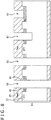
- FIG. 6 depicts a cross sectional view of the first semiconductor substrate 51 before a through-hole 61 for forming a through electrode 52 is opened.
- a protection diode structure that can be formed in a MOS transistor formation process is formed in a first semiconductor substrate 51 as depicted in FIG. 6 .
- an STI 21 that is formed in a recessed shape individually at each position at which each through electrode 52 is to be formed in the first semiconductor substrate 51, and an N+ diffusion layer 41 is formed in each recessed portion of the STI 21.
- the recessed portions of the STI 21 are formed with a depth sufficient to isolate the N+ diffusion layers 41, each of which is to be disposed around each through electrode 53, from each other, the protection diode structures that are formed around the through electrodes 53 are maintained in a mutually isolated state.
- each recessed portion of the STI 21 is formed in accordance with a cross sectional shape of the through electrode 52 to be formed in the recessed portion.
- the sectional shape of the through electrode 52 is a circular shape
- the recessed portions of the STI 21 and the N+ diffusion layer 41 are also formed in a circular shape as depicted in FIG. 7 .
- a P well region 22 is formed on an upper layer of the STI 21 and the N+ diffusion layer 41. Consequently, at positions at which the through electrodes 52 are to be formed, protection diode structures separate from and independent of each other are formed individually for the through electrodes 52 by the recessed portions of the STI 21.
- the first semiconductor substrate 51 in which the protection diode structures are formed and a second semiconductor substrate (not depicted) to be stacked on the same are pasted to each other with circuit faces thereof opposed to each other.
- the P well region 22 of the Si substrate 51 is made thinner to a desired thickness, and then, through-holes 61 extending from the P well region 22 and the N+ diffusion layer 41 of the first semiconductor substrate 51 to the second semiconductor substrate are opened at the positions of the through electrodes 52 by dry etching.
- a side wall insulating film 23 such as an SiO 2 film or an SiN film is deposited on a side wall of each of the opened through-holes 61, and then, an electrode material 24 is filled to form through electrodes 52.
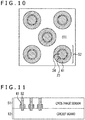
- FIG. 10 is a sectional view of the through electrodes 52 formed at recessed portions of the STI 21 in the first semiconductor substrate 51.
- a side wall insulating film 23, an N+ diffusion layer 41, and an STI 21 are formed in this order around the electrode material 24 that forms each of the through electrodes 52. More specifically, since a junction potential barrier by the N+ diffusion layer 41 is present between the side wall insulating film 23 and the STI 21, movement of charge from the P well region 22 to the STI 21, which has occurred upon opening of a through-hole in the related-art configuration, is suppressed.
- the N+ diffusion layers 41 around the through electrodes 52 are electrically isolated from each other by the recessed portions of the STI 21, even if timings at which a plurality of through-holes reaches the STI 21 suffer from dispersion, charge dispersed in the P well region 22 is not concentrated upon the through-hole that reaches the P well region 22 first, and a dispersed state is maintained.
- FIG. 11 depicts a sectional view of a first configuration example of the solid-state imaging element that is an embodiment of the present technology.
- a first semiconductor substrate 51 on which a CMOS image sensor including a PD (photodiode), a pixel transistor, and so forth is formed and which has a protection diode structure and a second semiconductor substrate 12 including various signal processing circuits and so forth are pasted to and stacked on each other, and through-holes are opened from the rear face side (upper side in FIG. 11 ) of the first semiconductor substrate 51 to form through electrodes 52.
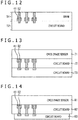
- FIG. 12 depicts a sectional view of a configuration example of a semiconductor device that is an embodiment of the present technology.
- a first semiconductor substrate 51 on which a semiconductor memory represented by a DRAM is formed and which has a protection diode structure and a second semiconductor substrate 12 including various signal processing circuits and so forth are stacked on each other, and through-holes are opened from the rear face side (upper side in FIG. 12 ) of the first semiconductor substrate 51 to form through electrodes 52.
- FIG. 13 depicts a sectional view of a second configuration example of a solid-state imaging element that is an embodiment of the present technology.
- CMOS image sensor substrate 71 including PDs, pixel transistors, and so forth and a circuit board 72 (corresponding to the first semiconductor substrate 11) having a protection diode structure are pasted to and stacked on each other, and through-holes are opened from the side of the circuit board 72 on which the CMOS image sensor substrate 71 is not stacked to form through electrodes 52.
- FIG. 14 depicts a sectional view of a third configuration example of a solid-state imaging element that is an embodiment of the present technology.
- CMOS image sensor substrate 81 including PDs, pixel transistors, and so forth and a circuit board 82 (corresponding to the first semiconductor substrate 11) having a protection diode structure are pasted to and stacked on each other, and through-holes are opened from the side of the circuit board 82 on which the CMOS image sensor substrate 81 is not stacked to form through electrodes 52.
- circuit board 82 on which the CMOS image sensor substrate 81 is not stacked a circuit board chip 83 on which connection pads to the through electrode 52 are exposed is pasted.
- the technology according to the present disclosure can be applied to various produces.
- the technology according to the present disclosure may be applied to an endoscopic surgery system.
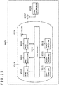
- FIG. 15 is a block diagram depicting an example of a schematic configuration of an in-vivo information acquisition system of a patient using a capsule type endoscope, to which the technology according to an embodiment of the present disclosure (present technology) can be applied.
- the in-vivo information acquisition system 10001 includes a capsule type endoscope 10100 and an external controlling apparatus 10200.
- the capsule type endoscope 10100 is swallowed by a patient at the time of inspection.
- the capsule type endoscope 10100 has an image pickup function and a wireless communication function and successively picks up an image of the inside of an organ such as the stomach or an intestine (hereinafter referred to as in-vivo image) at predetermined intervals while it moves inside of the organ by peristaltic motion for a period of time until it is naturally discharged from the patient. Then, the capsule type endoscope 10100 successively transmits information of the in-vivo image to the external controlling apparatus 10200 outside the body by wireless transmission.
- the external controlling apparatus 10200 integrally controls operation of the in-vivo information acquisition system 10001. Further, the external controlling apparatus 10200 receives information of an in-vivo image transmitted thereto from the capsule type endoscope 10100 and generates image data for displaying the in-vivo image on a display apparatus (not depicted) on the basis of the received information of the in-vivo image.
- an in-vivo image imaged a state of the inside of the body of a patient can be acquired at any time in this manner for a period of time until the capsule type endoscope 10100 is discharged after it is swallowed.
- a configuration and functions of the capsule type endoscope 10100 and the external controlling apparatus 10200 are described in more detail below.
- the capsule type endoscope 10100 includes a housing 10101 of the capsule type, in which a light source unit 10111, an image pickup unit 10112, an image processing unit 10113, a wireless communication unit 10114, a power feeding unit 10115, a power supply unit 10116 and a control unit 10117 are accommodated.
- the light source unit 10111 includes a light source such as, for example, a light emitting diode (LED) and irradiates light on an image pickup field-of-view of the image pickup unit 10112.
- a light source such as, for example, a light emitting diode (LED) and irradiates light on an image pickup field-of-view of the image pickup unit 10112.
- LED light emitting diode
- the image pickup unit 10112 includes an image pickup element and an optical system including a plurality of lenses provided at a preceding stage to the image pickup element.
- Reflected light hereinafter referred to as observation light
- the incident observation light is photoelectrically converted by the image pickup element, by which an image signal corresponding to the observation light is generated.
- the image signal generated by the image pickup unit 10112 is provided to the image processing unit 10113.
- the image processing unit 10113 includes a processor such as a central processing unit (CPU) or a graphics processing unit (GPU) and performs various signal processes for an image signal generated by the image pickup unit 10112.
- the image processing unit 10113 provides the image signal for which the signal processes have been performed thereby as RAW data to the wireless communication unit 10114.
- the wireless communication unit 10114 performs a predetermined process such as a modulation process for the image signal for which the signal processes have been performed by the image processing unit 10113 and transmits the resulting image signal to the external controlling apparatus 10200 through an antenna 10114A. Further, the wireless communication unit 10114 receives a control signal relating to driving control of the capsule type endoscope 10100 from the external controlling apparatus 10200 through the antenna 10114A. The wireless communication unit 10114 provides the control signal received from the external controlling apparatus 10200 to the control unit 10117.
- a predetermined process such as a modulation process for the image signal for which the signal processes have been performed by the image processing unit 10113 and transmits the resulting image signal to the external controlling apparatus 10200 through an antenna 10114A. Further, the wireless communication unit 10114 receives a control signal relating to driving control of the capsule type endoscope 10100 from the external controlling apparatus 10200 through the antenna 10114A. The wireless communication unit 10114 provides the control signal received from the external controlling apparatus 10200 to the control unit 10117.
- the power feeding unit 10115 includes an antenna coil for power reception, a power regeneration circuit for regenerating electric power from current generated in the antenna coil, a voltage booster circuit and so forth.
- the power feeding unit 10115 generates electric power using the principle of non-contact charging.
- the power supply unit 10116 includes a secondary battery and stores electric power generated by the power feeding unit 10115.
- FIG. 15 in order to avoid complicated illustration, an arrow mark indicative of a supply destination of electric power from the power supply unit 10116 and so forth are omitted.
- electric power stored in the power supply unit 10116 is supplied to and can be used to drive the light source unit 10111, the image pickup unit 10112, the image processing unit 10113, the wireless communication unit 10114 and the control unit 10117.
- the control unit 10117 includes a processor such as a CPU and suitably controls driving of the light source unit 10111, the image pickup unit 10112, the image processing unit 10113, the wireless communication unit 10114 and the power feeding unit 10115 in accordance with a control signal transmitted thereto from the external controlling apparatus 10200.
- a processor such as a CPU and suitably controls driving of the light source unit 10111, the image pickup unit 10112, the image processing unit 10113, the wireless communication unit 10114 and the power feeding unit 10115 in accordance with a control signal transmitted thereto from the external controlling apparatus 10200.
- the external controlling apparatus 10200 includes a processor such as a CPU or a GPU, a microcomputer, a control board or the like in which a processor and a storage element such as a memory are mixedly incorporated.
- the external controlling apparatus 10200 transmits a control signal to the control unit 10117 of the capsule type endoscope 10100 through an antenna 10200A to control operation of the capsule type endoscope 10100.
- an irradiation condition of light upon an observation target of the light source unit 10111 can be changed, for example, in accordance with a control signal from the external controlling apparatus 10200.
- an image pickup condition for example, a frame rate, an exposure value or the like of the image pickup unit 10112
- a control signal from the external controlling apparatus 10200 can be changed in accordance with a control signal from the external controlling apparatus 10200.
- the substance of processing by the image processing unit 10113 or a condition for transmitting an image signal from the wireless communication unit 10114 may be changed in accordance with a control signal from the external controlling apparatus 10200.
- the external controlling apparatus 10200 performs various image processes for an image signal transmitted thereto from the capsule type endoscope 10100 to generate image data for displaying a picked up in-vivo image on the display apparatus.
- various signal processes can be performed such as, for example, a development process (demosaic process), an image quality improving process (bandwidth enhancement process, a super-resolution process, a noise reduction (NR) process and/or image stabilization process) and/or an enlargement process (electronic zooming process).
- the external controlling apparatus 10200 controls driving of the display apparatus to cause the display apparatus to display a picked up in-vivo image on the basis of generated image data.
- the external controlling apparatus 10200 may also control a recording apparatus (not depicted) to record generated image data or control a printing apparatus (not depicted) to output generated image data by printing.
- the technology according to the present disclosure can be applied to various products.
- the technology according to the present disclosure may be implemented as an apparatus that is incorporated in any type of mobile body such as an automobile, an electric car, a hybrid electric car, a motorcycle, a bicycle, a personal mobility, an airplane, a drone, a ship, a robot, and so forth.
- FIG. 16 is a block diagram depicting an example of schematic configuration of a vehicle control system as an example of a mobile body control system to which the technology according to an embodiment of the present disclosure can be applied.
- the vehicle control system 12000 includes a plurality of electronic control units connected to each other via a communication network 12001.
- the vehicle control system 12000 includes a driving system control unit 12010, a body system control unit 12020, an outside-vehicle information detecting unit 12030, an in-vehicle information detecting unit 12040, and an integrated control unit 12050.
- a microcomputer 12051, a sound/image output section 12052, and a vehicle-mounted network interface (I/F) 12053 are illustrated as a functional configuration of the integrated control unit 12050.
- the driving system control unit 12010 controls the operation of devices related to the driving system of the vehicle in accordance with various kinds of programs.
- the driving system control unit 12010 functions as a control device for a driving force generating device for generating the driving force of the vehicle, such as an internal combustion engine, a driving motor, or the like, a driving force transmitting mechanism for transmitting the driving force to wheels, a steering mechanism for adjusting the steering angle of the vehicle, a braking device for generating the braking force of the vehicle, and the like.
- the body system control unit 12020 controls the operation of various kinds of devices provided to a vehicle body in accordance with various kinds of programs.
- the body system control unit 12020 functions as a control device for a keyless entry system, a smart key system, a power window device, or various kinds of lamps such as a headlamp, a backup lamp, a brake lamp, a turn signal, a fog lamp, or the like.
- radio waves transmitted from a mobile device as an alternative to a key or signals of various kinds of switches can be input to the body system control unit 12020.
- the body system control unit 12020 receives these input radio waves or signals, and controls a door lock device, the power window device, the lamps, or the like of the vehicle.
- the outside-vehicle information detecting unit 12030 detects information about the outside of the vehicle including the vehicle control system 12000.
- the outside-vehicle information detecting unit 12030 is connected with an imaging section 12031.
- the outside-vehicle information detecting unit 12030 makes the imaging section 12031 image an image of the outside of the vehicle, and receives the imaged image.
- the outside-vehicle information detecting unit 12030 may perform processing of detecting an object such as a human, a vehicle, an obstacle, a sign, a character on a road surface, or the like, or processing of detecting a distance thereto.
- the imaging section 12031 is an optical sensor that receives light, and which outputs an electric signal corresponding to a received light amount of the light.
- the imaging section 12031 can output the electric signal as an image, or can output the electric signal as information about a measured distance.
- the light received by the imaging section 12031 may be visible light, or may be invisible light such as infrared rays or the like.
- the in-vehicle information detecting unit 12040 detects information about the inside of the vehicle.
- the in-vehicle information detecting unit 12040 is, for example, connected with a driver state detecting section 12041 that detects the state of a driver.
- the driver state detecting section 12041 for example, includes a camera that images the driver.
- the in-vehicle information detecting unit 12040 may calculate a degree of fatigue of the driver or a degree of concentration of the driver, or may determine whether the driver is dozing.
- the microcomputer 12051 can calculate a control target value for the driving force generating device, the steering mechanism, or the braking device on the basis of the information about the inside or outside of the vehicle which information is obtained by the outside-vehicle information detecting unit 12030 or the in-vehicle information detecting unit 12040, and output a control command to the driving system control unit 12010.
- the microcomputer 12051 can perform cooperative control intended to implement functions of an advanced driver assistance system (ADAS) which functions include collision avoidance or shock mitigation for the vehicle, following driving based on a following distance, vehicle speed maintaining driving, a warning of collision of the vehicle, a warning of deviation of the vehicle from a lane, or the like.
- ADAS advanced driver assistance system
- the microcomputer 12051 can perform cooperative control intended for automatic driving, which makes the vehicle to travel autonomously without depending on the operation of the driver, or the like, by controlling the driving force generating device, the steering mechanism, the braking device, or the like on the basis of the information about the outside or inside of the vehicle which information is obtained by the outside-vehicle information detecting unit 12030 or the in-vehicle information detecting unit 12040.
- the microcomputer 12051 can output a control command to the body system control unit 12020 on the basis of the information about the outside of the vehicle which information is obtained by the outside-vehicle information detecting unit 12030.
- the microcomputer 12051 can perform cooperative control intended to prevent a glare by controlling the headlamp so as to change from a high beam to a low beam, for example, in accordance with the position of a preceding vehicle or an oncoming vehicle detected by the outside-vehicle information detecting unit 12030.
- the sound/image output section 12052 transmits an output signal of at least one of a sound and an image to an output device capable of visually or auditorily notifying information to an occupant of the vehicle or the outside of the vehicle.
- an audio speaker 12061, a display section 12062, and an instrument panel 12063 are illustrated as the output device.
- the display section 12062 may, for example, include at least one of an on-board display and a head-up display.
- FIG. 17 is a diagram depicting an example of the installation position of the imaging section 12031.
- the imaging section 12031 includes imaging sections 12101, 12102, 12103, 12104, and 12105.
- the imaging sections 12101, 12102, 12103, 12104, and 12105 are, for example, disposed at positions on a front nose, sideview mirrors, a rear bumper, and a back door of the vehicle 12100 as well as a position on an upper portion of a windshield within the interior of the vehicle.
- the imaging section 12101 provided to the front nose and the imaging section 12105 provided to the upper portion of the windshield within the interior of the vehicle obtain mainly an image of the front of the vehicle 12100.
- the imaging sections 12102 and 12103 provided to the sideview mirrors obtain mainly an image of the sides of the vehicle 12100.
- the imaging section 12104 provided to the rear bumper or the back door obtains mainly an image of the rear of the vehicle 12100.
- the imaging section 12105 provided to the upper portion of the windshield within the interior of the vehicle is used mainly to detect a preceding vehicle, a pedestrian, an obstacle, a signal, a traffic sign, a lane, or the like.
- FIG. 17 depicts an example of photographing ranges of the imaging sections 12101 to 12104.
- An imaging range 12111 represents the imaging range of the imaging section 12101 provided to the front nose.
- Imaging ranges 12112 and 12113 respectively represent the imaging ranges of the imaging sections 12102 and 12103 provided to the sideview mirrors.
- An imaging range 12114 represents the imaging range of the imaging section 12104 provided to the rear bumper or the back door.
- a bird's-eye image of the vehicle 12100 as viewed from above is obtained by superimposing image data imaged by the imaging sections 12101 to 12104, for example.
- At least one of the imaging sections 12101 to 12104 may have a function of obtaining distance information.
- at least one of the imaging sections 12101 to 12104 may be a stereo camera constituted of a plurality of imaging elements, or may be an imaging element having pixels for phase difference detection.
- the microcomputer 12051 can determine a distance to each three-dimensional object within the imaging ranges 12111 to 12114 and a temporal change in the distance (relative speed with respect to the vehicle 12100) on the basis of the distance information obtained from the imaging sections 12101 to 12104, and thereby extract, as a preceding vehicle, a nearest three-dimensional object in particular that is present on a traveling path of the vehicle 12100 and which travels in substantially the same direction as the vehicle 12100 at a predetermined speed (for example, equal to or more than 0 km/hour). Further, the microcomputer 12051 can set a following distance to be maintained in front of a preceding vehicle in advance, and perform automatic brake control (including following stop control), automatic acceleration control (including following start control), or the like. It is thus possible to perform cooperative control intended for automatic driving that makes the vehicle travel autonomously without depending on the operation of the driver or the like.
- automatic brake control including following stop control
- automatic acceleration control including following start control
- the microcomputer 12051 can classify three-dimensional object data on three-dimensional objects into three-dimensional object data of a two-wheeled vehicle, a standard-sized vehicle, a large-sized vehicle, a pedestrian, a utility pole, and other three-dimensional objects on the basis of the distance information obtained from the imaging sections 12101 to 12104, extract the classified three-dimensional object data, and use the extracted three-dimensional object data for automatic avoidance of an obstacle.
- the microcomputer 12051 identifies obstacles around the vehicle 12100 as obstacles that the driver of the vehicle 12100 can recognize visually and obstacles that are difficult for the driver of the vehicle 12100 to recognize visually. Then, the microcomputer 12051 determines a collision risk indicating a risk of collision with each obstacle.
- the microcomputer 12051 In a situation in which the collision risk is equal to or higher than a set value and there is thus a possibility of collision, the microcomputer 12051 outputs a warning to the driver via the audio speaker 12061 or the display section 12062, and performs forced deceleration or avoidance steering via the driving system control unit 12010. The microcomputer 12051 can thereby assist in driving to avoid collision.
- At least one of the imaging sections 12101 to 12104 may be an infrared camera that detects infrared rays.
- the microcomputer 12051 can, for example, recognize a pedestrian by determining whether or not there is a pedestrian in imaged images of the imaging sections 12101 to 12104. Such recognition of a pedestrian is, for example, performed by a procedure of extracting characteristic points in the imaged images of the imaging sections 12101 to 12104 as infrared cameras and a procedure of determining whether or not it is the pedestrian by performing pattern matching processing on a series of characteristic points representing the contour of the object.
- the sound/image output section 12052 controls the display section 12062 so that a square contour line for emphasis is displayed so as to be superimposed on the recognized pedestrian.
- the sound/image output section 12052 may also control the display section 12062 so that an icon or the like representing the pedestrian is displayed at a desired position.
- First semiconductor substrate 12 Second semiconductor substrate, 13 Through electrode, 21 STI, 22 P well region, 23 Side wall insulating film, 24 Electrode material, 31 Through-hole, 41 N+ diffusion layer, 51 First semiconductor substrate, 52 Through electrode, 61 Through-hole
Landscapes
- Engineering & Computer Science (AREA)
- Multimedia (AREA)
- Signal Processing (AREA)
- Solid State Image Pick-Up Elements (AREA)
- Manufacturing & Machinery (AREA)
- Internal Circuitry In Semiconductor Integrated Circuit Devices (AREA)
- Transforming Light Signals Into Electric Signals (AREA)
- Semiconductor Integrated Circuits (AREA)
Applications Claiming Priority (2)
| Application Number | Priority Date | Filing Date | Title |
|---|---|---|---|
| JP2017010053 | 2017-01-24 | ||
| PCT/JP2018/000232 WO2018139188A1 (ja) | 2017-01-24 | 2018-01-10 | 半導体装置および製造方法、固体撮像素子、並びに電子機器 |
Publications (3)
| Publication Number | Publication Date |
|---|---|
| EP3576151A1 true EP3576151A1 (de) | 2019-12-04 |
| EP3576151A4 EP3576151A4 (de) | 2020-06-03 |
| EP3576151B1 EP3576151B1 (de) | 2024-11-06 |
Family
ID=62979346
Family Applications (1)
| Application Number | Title | Priority Date | Filing Date |
|---|---|---|---|
| EP18744431.0A Active EP3576151B1 (de) | 2017-01-24 | 2018-01-10 | Halbleiterbauelement, verfahren zur herstellung davon, festkörperbildaufnahmeelement und elektronische vorrichtung |
Country Status (6)
| Country | Link |
|---|---|
| US (2) | US10916538B2 (de) |
| EP (1) | EP3576151B1 (de) |
| JP (1) | JP7123813B2 (de) |
| KR (1) | KR102498387B1 (de) |
| CN (1) | CN110199392B (de) |
| WO (1) | WO2018139188A1 (de) |
Families Citing this family (5)
| Publication number | Priority date | Publication date | Assignee | Title |
|---|---|---|---|---|
| CN110199392B (zh) * | 2017-01-24 | 2023-05-12 | 索尼半导体解决方案公司 | 半导体装置及其制造方法、固态成像元件和电子设备 |
| JP2021068737A (ja) * | 2019-10-17 | 2021-04-30 | 本田技研工業株式会社 | 半導体装置 |
| JP7510820B2 (ja) * | 2020-08-31 | 2024-07-04 | シャープ福山レーザー株式会社 | 画像表示素子 |
| JP7434118B2 (ja) * | 2020-09-11 | 2024-02-20 | ルネサスエレクトロニクス株式会社 | 半導体装置 |
| WO2025258351A1 (ja) * | 2024-06-10 | 2025-12-18 | ソニーセミコンダクタソリューションズ株式会社 | 半導体装置、固体撮像素子及び電子機器 |
Family Cites Families (18)
| Publication number | Priority date | Publication date | Assignee | Title |
|---|---|---|---|---|
| JP3840203B2 (ja) * | 2002-06-27 | 2006-11-01 | キヤノン株式会社 | 固体撮像装置及び固体撮像装置を用いたカメラシステム |
| JP2007250561A (ja) * | 2004-04-12 | 2007-09-27 | Japan Science & Technology Agency | 半導体素子および半導体システム |
| KR101046798B1 (ko) * | 2008-09-30 | 2011-07-05 | 주식회사 동부하이텍 | 이미지센서 및 그 제조방법 |
| KR101024770B1 (ko) * | 2008-09-30 | 2011-03-24 | 주식회사 동부하이텍 | 이미지센서 및 그 제조방법 |
| TWI445166B (zh) * | 2008-11-07 | 2014-07-11 | Sony Corp | 固態成像裝置,製造固態成像裝置之方法、及電子設備 |
| TWI372457B (en) * | 2009-03-20 | 2012-09-11 | Ind Tech Res Inst | Esd structure for 3d ic tsv device |
| TWI515885B (zh) * | 2009-12-25 | 2016-01-01 | 新力股份有限公司 | 半導體元件及其製造方法,及電子裝置 |
| JP5853351B2 (ja) | 2010-03-25 | 2016-02-09 | ソニー株式会社 | 半導体装置、半導体装置の製造方法、及び電子機器 |
| US8441104B1 (en) * | 2011-11-16 | 2013-05-14 | Analog Devices, Inc. | Electrical overstress protection using through-silicon-via (TSV) |
| JP2013157422A (ja) * | 2012-01-30 | 2013-08-15 | Sony Corp | 固体撮像素子、固体撮像素子の製造方法、および電子機器 |
| JP6012262B2 (ja) | 2012-05-31 | 2016-10-25 | キヤノン株式会社 | 半導体装置の製造方法 |
| KR102013770B1 (ko) * | 2012-08-30 | 2019-08-23 | 에스케이하이닉스 주식회사 | 반도체 소자 및 그 제조 방법 |
| JP6079502B2 (ja) * | 2013-08-19 | 2017-02-15 | ソニー株式会社 | 固体撮像素子および電子機器 |
| US20150257023A1 (en) | 2013-11-01 | 2015-09-10 | Sony Corporation | Distribution of network status and information in wlan networks for self-optimization/organization |
| TWI706550B (zh) * | 2013-11-06 | 2020-10-01 | 日商新力股份有限公司 | 固體攝像裝置及其製造方法、及電子機器 |
| US10361244B2 (en) | 2014-07-15 | 2019-07-23 | Brillinics Inc. | Solid-state imaging device, method for producing solid-state imaging device, and electronic apparatus |
| US10658296B2 (en) * | 2016-09-30 | 2020-05-19 | Taiwan Semiconductor Manufacturing Co., Ltd. | Dielectric film for semiconductor fabrication |
| CN110199392B (zh) * | 2017-01-24 | 2023-05-12 | 索尼半导体解决方案公司 | 半导体装置及其制造方法、固态成像元件和电子设备 |
-
2018
- 2018-01-10 CN CN201880007138.0A patent/CN110199392B/zh active Active
- 2018-01-10 KR KR1020197019747A patent/KR102498387B1/ko active Active
- 2018-01-10 JP JP2018564457A patent/JP7123813B2/ja active Active
- 2018-01-10 EP EP18744431.0A patent/EP3576151B1/de active Active
- 2018-01-10 US US16/477,963 patent/US10916538B2/en active Active
- 2018-01-10 WO PCT/JP2018/000232 patent/WO2018139188A1/ja not_active Ceased
-
2021
- 2021-01-05 US US17/141,675 patent/US11605625B2/en active Active
Also Published As
| Publication number | Publication date |
|---|---|
| KR20190107667A (ko) | 2019-09-20 |
| CN110199392A (zh) | 2019-09-03 |
| US20200126969A1 (en) | 2020-04-23 |
| EP3576151B1 (de) | 2024-11-06 |
| KR102498387B1 (ko) | 2023-02-13 |
| EP3576151A4 (de) | 2020-06-03 |
| JP7123813B2 (ja) | 2022-08-23 |
| CN110199392B (zh) | 2023-05-12 |
| JPWO2018139188A1 (ja) | 2019-11-14 |
| US11605625B2 (en) | 2023-03-14 |
| WO2018139188A1 (ja) | 2018-08-02 |
| US10916538B2 (en) | 2021-02-09 |
| US20210125978A1 (en) | 2021-04-29 |
Similar Documents
| Publication | Publication Date | Title |
|---|---|---|
| US12100718B2 (en) | Solid state image sensor having a grid-patterned inter-pixel isolation section separating the photoelectric conversion sections of each of the pixels from one another and provided with protruding sections | |
| US11605625B2 (en) | Semiconductor device and manufacturing method therefor, solid-state imaging element, and electronic equipment | |
| JP6855287B2 (ja) | 固体撮像装置、および電子機器 | |
| US12396279B2 (en) | Solid-state image pickup apparatus and electronic equipment | |
| US11798968B2 (en) | Image pickup device and electronic apparatus | |
| KR102611545B1 (ko) | 촬상 장치 및 전자 기기 | |
| US10880506B2 (en) | Solid-state imaging device, electronic apparatus, and driving method | |
| US12490529B2 (en) | Solid-state imaging device and electronic apparatus having a storage capacitor with a thin insulating film | |
| US20220392936A1 (en) | Solid-state imaging device and method of producing the same | |
| US10991723B2 (en) | Semiconductor device, method of manufacturing semiconductor device, and electronic apparatus | |
| US12568702B2 (en) | Light reception element and electronic apparatus | |
| WO2025173400A1 (ja) | 光検出装置 | |
| CN115023813A (zh) | 摄像元件和半导体芯片 |
Legal Events
| Date | Code | Title | Description |
|---|---|---|---|
| STAA | Information on the status of an ep patent application or granted ep patent |
Free format text: STATUS: THE INTERNATIONAL PUBLICATION HAS BEEN MADE |
|
| PUAI | Public reference made under article 153(3) epc to a published international application that has entered the european phase |
Free format text: ORIGINAL CODE: 0009012 |
|
| STAA | Information on the status of an ep patent application or granted ep patent |
Free format text: STATUS: REQUEST FOR EXAMINATION WAS MADE |
|
| 17P | Request for examination filed |
Effective date: 20190814 |
|
| AK | Designated contracting states |
Kind code of ref document: A1 Designated state(s): AL AT BE BG CH CY CZ DE DK EE ES FI FR GB GR HR HU IE IS IT LI LT LU LV MC MK MT NL NO PL PT RO RS SE SI SK SM TR |
|
| AX | Request for extension of the european patent |
Extension state: BA ME |
|
| DAV | Request for validation of the european patent (deleted) | ||
| DAX | Request for extension of the european patent (deleted) | ||
| A4 | Supplementary search report drawn up and despatched |
Effective date: 20200508 |
|
| RIC1 | Information provided on ipc code assigned before grant |
Ipc: H01L 27/146 20060101AFI20200501BHEP Ipc: H04N 5/369 20110101ALI20200501BHEP Ipc: H01L 23/522 20060101ALI20200501BHEP Ipc: H01L 21/822 20060101ALI20200501BHEP Ipc: H01L 27/105 20060101ALI20200501BHEP Ipc: H01L 27/06 20060101ALI20200501BHEP Ipc: H01L 27/04 20060101ALI20200501BHEP Ipc: H01L 21/3205 20060101ALI20200501BHEP Ipc: H01L 21/768 20060101ALI20200501BHEP |
|
| STAA | Information on the status of an ep patent application or granted ep patent |
Free format text: STATUS: EXAMINATION IS IN PROGRESS |
|
| 17Q | First examination report despatched |
Effective date: 20211217 |
|
| GRAP | Despatch of communication of intention to grant a patent |
Free format text: ORIGINAL CODE: EPIDOSNIGR1 |
|
| STAA | Information on the status of an ep patent application or granted ep patent |
Free format text: STATUS: GRANT OF PATENT IS INTENDED |
|
| INTG | Intention to grant announced |
Effective date: 20240426 |
|
| RIC1 | Information provided on ipc code assigned before grant |
Ipc: H04N 25/70 20230101ALI20240415BHEP Ipc: H01L 27/02 20060101ALI20240415BHEP Ipc: H01L 27/105 20060101ALI20240415BHEP Ipc: H01L 27/06 20060101ALI20240415BHEP Ipc: H01L 27/04 20060101ALI20240415BHEP Ipc: H01L 23/522 20060101ALI20240415BHEP Ipc: H01L 21/822 20060101ALI20240415BHEP Ipc: H01L 21/768 20060101ALI20240415BHEP Ipc: H01L 21/3205 20060101ALI20240415BHEP Ipc: H01L 27/146 20060101AFI20240415BHEP |
|
| RIN1 | Information on inventor provided before grant (corrected) |
Inventor name: TAKAHASHI, HIROSHI |
|
| GRAJ | Information related to disapproval of communication of intention to grant by the applicant or resumption of examination proceedings by the epo deleted |
Free format text: ORIGINAL CODE: EPIDOSDIGR1 |
|
| STAA | Information on the status of an ep patent application or granted ep patent |
Free format text: STATUS: EXAMINATION IS IN PROGRESS |
|
| P01 | Opt-out of the competence of the unified patent court (upc) registered |
Free format text: CASE NUMBER: APP_44296/2024 Effective date: 20240730 |
|
| STAA | Information on the status of an ep patent application or granted ep patent |
Free format text: STATUS: GRANT OF PATENT IS INTENDED |
|
| GRAS | Grant fee paid |
Free format text: ORIGINAL CODE: EPIDOSNIGR3 |
|
| INTC | Intention to grant announced (deleted) | ||
| GRAA | (expected) grant |
Free format text: ORIGINAL CODE: 0009210 |
|
| STAA | Information on the status of an ep patent application or granted ep patent |
Free format text: STATUS: THE PATENT HAS BEEN GRANTED |
|
| AK | Designated contracting states |
Kind code of ref document: B1 Designated state(s): AL AT BE BG CH CY CZ DE DK EE ES FI FR GB GR HR HU IE IS IT LI LT LU LV MC MK MT NL NO PL PT RO RS SE SI SK SM TR |
|
| REG | Reference to a national code |
Ref country code: GB Ref legal event code: FG4D |
|
| REG | Reference to a national code |
Ref country code: CH Ref legal event code: EP |
|
| REG | Reference to a national code |
Ref country code: DE Ref legal event code: R079 Ref document number: 602018076267 Country of ref document: DE Free format text: PREVIOUS MAIN CLASS: H01L0027146000 Ipc: H10F0039180000 |
|
| REG | Reference to a national code |
Ref country code: DE Ref legal event code: R096 Ref document number: 602018076267 Country of ref document: DE |
|
| REG | Reference to a national code |
Ref country code: IE Ref legal event code: FG4D |
|
| PGFP | Annual fee paid to national office [announced via postgrant information from national office to epo] |
Ref country code: NL Payment date: 20241219 Year of fee payment: 8 |
|
| REG | Reference to a national code |
Ref country code: LT Ref legal event code: MG9D |
|
| REG | Reference to a national code |
Ref country code: NL Ref legal event code: MP Effective date: 20241106 |
|
| PG25 | Lapsed in a contracting state [announced via postgrant information from national office to epo] |
Ref country code: PT Free format text: LAPSE BECAUSE OF FAILURE TO SUBMIT A TRANSLATION OF THE DESCRIPTION OR TO PAY THE FEE WITHIN THE PRESCRIBED TIME-LIMIT Effective date: 20250306 Ref country code: IS Free format text: LAPSE BECAUSE OF FAILURE TO SUBMIT A TRANSLATION OF THE DESCRIPTION OR TO PAY THE FEE WITHIN THE PRESCRIBED TIME-LIMIT Effective date: 20250306 Ref country code: HR Free format text: LAPSE BECAUSE OF FAILURE TO SUBMIT A TRANSLATION OF THE DESCRIPTION OR TO PAY THE FEE WITHIN THE PRESCRIBED TIME-LIMIT Effective date: 20241106 |
|
| PG25 | Lapsed in a contracting state [announced via postgrant information from national office to epo] |
Ref country code: FI Free format text: LAPSE BECAUSE OF FAILURE TO SUBMIT A TRANSLATION OF THE DESCRIPTION OR TO PAY THE FEE WITHIN THE PRESCRIBED TIME-LIMIT Effective date: 20241106 Ref country code: NL Free format text: LAPSE BECAUSE OF FAILURE TO SUBMIT A TRANSLATION OF THE DESCRIPTION OR TO PAY THE FEE WITHIN THE PRESCRIBED TIME-LIMIT Effective date: 20241106 |
|
| REG | Reference to a national code |
Ref country code: AT Ref legal event code: MK05 Ref document number: 1740382 Country of ref document: AT Kind code of ref document: T Effective date: 20241106 |
|
| PG25 | Lapsed in a contracting state [announced via postgrant information from national office to epo] |
Ref country code: BG Free format text: LAPSE BECAUSE OF FAILURE TO SUBMIT A TRANSLATION OF THE DESCRIPTION OR TO PAY THE FEE WITHIN THE PRESCRIBED TIME-LIMIT Effective date: 20241106 |
|
| PG25 | Lapsed in a contracting state [announced via postgrant information from national office to epo] |
Ref country code: ES Free format text: LAPSE BECAUSE OF FAILURE TO SUBMIT A TRANSLATION OF THE DESCRIPTION OR TO PAY THE FEE WITHIN THE PRESCRIBED TIME-LIMIT Effective date: 20241106 |
|
| PG25 | Lapsed in a contracting state [announced via postgrant information from national office to epo] |
Ref country code: NO Free format text: LAPSE BECAUSE OF FAILURE TO SUBMIT A TRANSLATION OF THE DESCRIPTION OR TO PAY THE FEE WITHIN THE PRESCRIBED TIME-LIMIT Effective date: 20250206 |
|
| PG25 | Lapsed in a contracting state [announced via postgrant information from national office to epo] |
Ref country code: LV Free format text: LAPSE BECAUSE OF FAILURE TO SUBMIT A TRANSLATION OF THE DESCRIPTION OR TO PAY THE FEE WITHIN THE PRESCRIBED TIME-LIMIT Effective date: 20241106 Ref country code: GR Free format text: LAPSE BECAUSE OF FAILURE TO SUBMIT A TRANSLATION OF THE DESCRIPTION OR TO PAY THE FEE WITHIN THE PRESCRIBED TIME-LIMIT Effective date: 20250207 Ref country code: AT Free format text: LAPSE BECAUSE OF FAILURE TO SUBMIT A TRANSLATION OF THE DESCRIPTION OR TO PAY THE FEE WITHIN THE PRESCRIBED TIME-LIMIT Effective date: 20241106 |
|
| PG25 | Lapsed in a contracting state [announced via postgrant information from national office to epo] |
Ref country code: PL Free format text: LAPSE BECAUSE OF FAILURE TO SUBMIT A TRANSLATION OF THE DESCRIPTION OR TO PAY THE FEE WITHIN THE PRESCRIBED TIME-LIMIT Effective date: 20241106 |
|
| PG25 | Lapsed in a contracting state [announced via postgrant information from national office to epo] |
Ref country code: RS Free format text: LAPSE BECAUSE OF FAILURE TO SUBMIT A TRANSLATION OF THE DESCRIPTION OR TO PAY THE FEE WITHIN THE PRESCRIBED TIME-LIMIT Effective date: 20250206 |
|
| PG25 | Lapsed in a contracting state [announced via postgrant information from national office to epo] |
Ref country code: SM Free format text: LAPSE BECAUSE OF FAILURE TO SUBMIT A TRANSLATION OF THE DESCRIPTION OR TO PAY THE FEE WITHIN THE PRESCRIBED TIME-LIMIT Effective date: 20241106 |
|
| PG25 | Lapsed in a contracting state [announced via postgrant information from national office to epo] |
Ref country code: DK Free format text: LAPSE BECAUSE OF FAILURE TO SUBMIT A TRANSLATION OF THE DESCRIPTION OR TO PAY THE FEE WITHIN THE PRESCRIBED TIME-LIMIT Effective date: 20241106 |
|
| PG25 | Lapsed in a contracting state [announced via postgrant information from national office to epo] |
Ref country code: EE Free format text: LAPSE BECAUSE OF FAILURE TO SUBMIT A TRANSLATION OF THE DESCRIPTION OR TO PAY THE FEE WITHIN THE PRESCRIBED TIME-LIMIT Effective date: 20241106 |
|
| PG25 | Lapsed in a contracting state [announced via postgrant information from national office to epo] |
Ref country code: RO Free format text: LAPSE BECAUSE OF FAILURE TO SUBMIT A TRANSLATION OF THE DESCRIPTION OR TO PAY THE FEE WITHIN THE PRESCRIBED TIME-LIMIT Effective date: 20241106 |
|
| PG25 | Lapsed in a contracting state [announced via postgrant information from national office to epo] |
Ref country code: SK Free format text: LAPSE BECAUSE OF FAILURE TO SUBMIT A TRANSLATION OF THE DESCRIPTION OR TO PAY THE FEE WITHIN THE PRESCRIBED TIME-LIMIT Effective date: 20241106 |
|
| PG25 | Lapsed in a contracting state [announced via postgrant information from national office to epo] |
Ref country code: CZ Free format text: LAPSE BECAUSE OF FAILURE TO SUBMIT A TRANSLATION OF THE DESCRIPTION OR TO PAY THE FEE WITHIN THE PRESCRIBED TIME-LIMIT Effective date: 20241106 |
|
| PG25 | Lapsed in a contracting state [announced via postgrant information from national office to epo] |
Ref country code: IT Free format text: LAPSE BECAUSE OF FAILURE TO SUBMIT A TRANSLATION OF THE DESCRIPTION OR TO PAY THE FEE WITHIN THE PRESCRIBED TIME-LIMIT Effective date: 20241106 |
|
| REG | Reference to a national code |
Ref country code: DE Ref legal event code: R097 Ref document number: 602018076267 Country of ref document: DE |
|
| REG | Reference to a national code |
Ref country code: CH Ref legal event code: PL |
|
| PG25 | Lapsed in a contracting state [announced via postgrant information from national office to epo] |
Ref country code: SE Free format text: LAPSE BECAUSE OF FAILURE TO SUBMIT A TRANSLATION OF THE DESCRIPTION OR TO PAY THE FEE WITHIN THE PRESCRIBED TIME-LIMIT Effective date: 20241106 |
|
| PLBE | No opposition filed within time limit |
Free format text: ORIGINAL CODE: 0009261 |
|
| STAA | Information on the status of an ep patent application or granted ep patent |
Free format text: STATUS: NO OPPOSITION FILED WITHIN TIME LIMIT |
|
| PG25 | Lapsed in a contracting state [announced via postgrant information from national office to epo] |
Ref country code: MC Free format text: LAPSE BECAUSE OF FAILURE TO SUBMIT A TRANSLATION OF THE DESCRIPTION OR TO PAY THE FEE WITHIN THE PRESCRIBED TIME-LIMIT Effective date: 20241106 Ref country code: LU Free format text: LAPSE BECAUSE OF NON-PAYMENT OF DUE FEES Effective date: 20250110 |
|
| 26N | No opposition filed |
Effective date: 20250807 |
|
| PG25 | Lapsed in a contracting state [announced via postgrant information from national office to epo] |
Ref country code: BE Free format text: LAPSE BECAUSE OF NON-PAYMENT OF DUE FEES Effective date: 20250131 |
|
| PG25 | Lapsed in a contracting state [announced via postgrant information from national office to epo] |
Ref country code: FR Free format text: LAPSE BECAUSE OF NON-PAYMENT OF DUE FEES Effective date: 20250131 |
|
| PG25 | Lapsed in a contracting state [announced via postgrant information from national office to epo] |
Ref country code: CH Free format text: LAPSE BECAUSE OF NON-PAYMENT OF DUE FEES Effective date: 20250131 |
|
| REG | Reference to a national code |
Ref country code: BE Ref legal event code: MM Effective date: 20250131 |
|
| GBPC | Gb: european patent ceased through non-payment of renewal fee |
Effective date: 20250206 |
|
| PG25 | Lapsed in a contracting state [announced via postgrant information from national office to epo] |
Ref country code: GB Free format text: LAPSE BECAUSE OF NON-PAYMENT OF DUE FEES Effective date: 20250206 |
|
| PG25 | Lapsed in a contracting state [announced via postgrant information from national office to epo] |
Ref country code: IE Free format text: LAPSE BECAUSE OF NON-PAYMENT OF DUE FEES Effective date: 20250110 |
|
| PGFP | Annual fee paid to national office [announced via postgrant information from national office to epo] |
Ref country code: DE Payment date: 20251217 Year of fee payment: 9 |