EP3575262B1 - Reduzierung des übersprechens in einem mixed-signal mehrchip mems-vorrichtungsgehäuse - Google Patents
Reduzierung des übersprechens in einem mixed-signal mehrchip mems-vorrichtungsgehäuse Download PDFInfo
- Publication number
- EP3575262B1 EP3575262B1 EP19174590.0A EP19174590A EP3575262B1 EP 3575262 B1 EP3575262 B1 EP 3575262B1 EP 19174590 A EP19174590 A EP 19174590A EP 3575262 B1 EP3575262 B1 EP 3575262B1
- Authority
- EP
- European Patent Office
- Prior art keywords
- bond pad
- signal
- die
- bearing
- chip
- Prior art date
- Legal status (The legal status is an assumption and is not a legal conclusion. Google has not performed a legal analysis and makes no representation as to the accuracy of the status listed.)
- Active
Links
Images


Classifications
-
- B—PERFORMING OPERATIONS; TRANSPORTING
- B81—MICROSTRUCTURAL TECHNOLOGY
- B81B—MICROSTRUCTURAL DEVICES OR SYSTEMS, e.g. MICROMECHANICAL DEVICES
- B81B7/00—Microstructural systems ; Auxiliary parts of microstructural devices or systems
- B81B7/0006—Interconnects
-
- B—PERFORMING OPERATIONS; TRANSPORTING
- B81—MICROSTRUCTURAL TECHNOLOGY
- B81B—MICROSTRUCTURAL DEVICES OR SYSTEMS, e.g. MICROMECHANICAL DEVICES
- B81B7/00—Microstructural systems ; Auxiliary parts of microstructural devices or systems
- B81B7/0032—Packages or encapsulation
- B81B7/0064—Packages or encapsulation for protecting against electromagnetic or electrostatic interferences
-
- B—PERFORMING OPERATIONS; TRANSPORTING
- B81—MICROSTRUCTURAL TECHNOLOGY
- B81B—MICROSTRUCTURAL DEVICES OR SYSTEMS, e.g. MICROMECHANICAL DEVICES
- B81B7/00—Microstructural systems ; Auxiliary parts of microstructural devices or systems
- B81B7/0032—Packages or encapsulation
- B81B7/007—Interconnections between the MEMS and external electrical signals
-
- B—PERFORMING OPERATIONS; TRANSPORTING
- B81—MICROSTRUCTURAL TECHNOLOGY
- B81B—MICROSTRUCTURAL DEVICES OR SYSTEMS, e.g. MICROMECHANICAL DEVICES
- B81B7/00—Microstructural systems ; Auxiliary parts of microstructural devices or systems
- B81B7/02—Microstructural systems ; Auxiliary parts of microstructural devices or systems containing distinct electrical or optical devices of particular relevance for their function, e.g. microelectro-mechanical systems [MEMS]
-
- B—PERFORMING OPERATIONS; TRANSPORTING
- B81—MICROSTRUCTURAL TECHNOLOGY
- B81C—PROCESSES OR APPARATUS SPECIALLY ADAPTED FOR THE MANUFACTURE OR TREATMENT OF MICROSTRUCTURAL DEVICES OR SYSTEMS
- B81C1/00—Manufacture or treatment of devices or systems in or on a substrate
- B81C1/00015—Manufacture or treatment of devices or systems in or on a substrate for manufacturing microsystems
- B81C1/00222—Integrating an electronic processing unit with a micromechanical structure
- B81C1/0023—Packaging together an electronic processing unit die and a micromechanical structure die
-
- B—PERFORMING OPERATIONS; TRANSPORTING
- B81—MICROSTRUCTURAL TECHNOLOGY
- B81C—PROCESSES OR APPARATUS SPECIALLY ADAPTED FOR THE MANUFACTURE OR TREATMENT OF MICROSTRUCTURAL DEVICES OR SYSTEMS
- B81C1/00—Manufacture or treatment of devices or systems in or on a substrate
- B81C1/00015—Manufacture or treatment of devices or systems in or on a substrate for manufacturing microsystems
- B81C1/00222—Integrating an electronic processing unit with a micromechanical structure
- B81C1/00246—Monolithic integration, i.e. micromechanical structure and electronic processing unit are integrated on the same substrate
-
- B—PERFORMING OPERATIONS; TRANSPORTING
- B81—MICROSTRUCTURAL TECHNOLOGY
- B81C—PROCESSES OR APPARATUS SPECIALLY ADAPTED FOR THE MANUFACTURE OR TREATMENT OF MICROSTRUCTURAL DEVICES OR SYSTEMS
- B81C1/00—Manufacture or treatment of devices or systems in or on a substrate
- B81C1/00015—Manufacture or treatment of devices or systems in or on a substrate for manufacturing microsystems
- B81C1/00261—Processes for packaging MEMS devices
- B81C1/00301—Connecting electric signal lines from the MEMS device with external electrical signal lines, e.g. through vias
-
- H—ELECTRICITY
- H04—ELECTRIC COMMUNICATION TECHNIQUE
- H04B—TRANSMISSION
- H04B1/00—Details of transmission systems, not covered by a single one of groups H04B3/00 - H04B13/00; Details of transmission systems not characterised by the medium used for transmission
- H04B1/06—Receivers
- H04B1/16—Circuits
-
- B—PERFORMING OPERATIONS; TRANSPORTING
- B81—MICROSTRUCTURAL TECHNOLOGY
- B81B—MICROSTRUCTURAL DEVICES OR SYSTEMS, e.g. MICROMECHANICAL DEVICES
- B81B2207/00—Microstructural systems or auxiliary parts thereof
- B81B2207/01—Microstructural systems or auxiliary parts thereof comprising a micromechanical device connected to control or processing electronics, i.e. Smart-MEMS
- B81B2207/012—Microstructural systems or auxiliary parts thereof comprising a micromechanical device connected to control or processing electronics, i.e. Smart-MEMS the micromechanical device and the control or processing electronics being separate parts in the same package
-
- B—PERFORMING OPERATIONS; TRANSPORTING
- B81—MICROSTRUCTURAL TECHNOLOGY
- B81B—MICROSTRUCTURAL DEVICES OR SYSTEMS, e.g. MICROMECHANICAL DEVICES
- B81B2207/00—Microstructural systems or auxiliary parts thereof
- B81B2207/07—Interconnects
-
- B—PERFORMING OPERATIONS; TRANSPORTING
- B81—MICROSTRUCTURAL TECHNOLOGY
- B81B—MICROSTRUCTURAL DEVICES OR SYSTEMS, e.g. MICROMECHANICAL DEVICES
- B81B2207/00—Microstructural systems or auxiliary parts thereof
- B81B2207/09—Packages
- B81B2207/091—Arrangements for connecting external electrical signals to mechanical structures inside the package
- B81B2207/098—Arrangements not provided for in groups B81B2207/092 - B81B2207/097
-
- B—PERFORMING OPERATIONS; TRANSPORTING
- B81—MICROSTRUCTURAL TECHNOLOGY
- B81C—PROCESSES OR APPARATUS SPECIALLY ADAPTED FOR THE MANUFACTURE OR TREATMENT OF MICROSTRUCTURAL DEVICES OR SYSTEMS
- B81C2203/00—Forming microstructural systems
- B81C2203/01—Packaging MEMS
- B81C2203/0154—Moulding a cap over the MEMS device
-
- H—ELECTRICITY
- H10—SEMICONDUCTOR DEVICES; ELECTRIC SOLID-STATE DEVICES NOT OTHERWISE PROVIDED FOR
- H10W—GENERIC PACKAGES, INTERCONNECTIONS, CONNECTORS OR OTHER CONSTRUCTIONAL DETAILS OF DEVICES COVERED BY CLASS H10
- H10W72/00—Interconnections or connectors in packages
- H10W72/50—Bond wires
- H10W72/541—Dispositions of bond wires
- H10W72/5445—Dispositions of bond wires being orthogonal to a side surface of the chip, e.g. parallel arrangements
-
- H—ELECTRICITY
- H10—SEMICONDUCTOR DEVICES; ELECTRIC SOLID-STATE DEVICES NOT OTHERWISE PROVIDED FOR
- H10W—GENERIC PACKAGES, INTERCONNECTIONS, CONNECTORS OR OTHER CONSTRUCTIONAL DETAILS OF DEVICES COVERED BY CLASS H10
- H10W90/00—Package configurations
- H10W90/701—Package configurations characterised by the relative positions of pads or connectors relative to package parts
- H10W90/751—Package configurations characterised by the relative positions of pads or connectors relative to package parts of bond wires
- H10W90/753—Package configurations characterised by the relative positions of pads or connectors relative to package parts of bond wires between laterally-adjacent chips
-
- H—ELECTRICITY
- H10—SEMICONDUCTOR DEVICES; ELECTRIC SOLID-STATE DEVICES NOT OTHERWISE PROVIDED FOR
- H10W—GENERIC PACKAGES, INTERCONNECTIONS, CONNECTORS OR OTHER CONSTRUCTIONAL DETAILS OF DEVICES COVERED BY CLASS H10
- H10W90/00—Package configurations
- H10W90/701—Package configurations characterised by the relative positions of pads or connectors relative to package parts
- H10W90/751—Package configurations characterised by the relative positions of pads or connectors relative to package parts of bond wires
- H10W90/756—Package configurations characterised by the relative positions of pads or connectors relative to package parts of bond wires between a chip and a stacked lead frame, conducting package substrate or heat sink
-
- H—ELECTRICITY
- H10—SEMICONDUCTOR DEVICES; ELECTRIC SOLID-STATE DEVICES NOT OTHERWISE PROVIDED FOR
- H10W—GENERIC PACKAGES, INTERCONNECTIONS, CONNECTORS OR OTHER CONSTRUCTIONAL DETAILS OF DEVICES COVERED BY CLASS H10
- H10W90/00—Package configurations
- H10W90/701—Package configurations characterised by the relative positions of pads or connectors relative to package parts
- H10W90/761—Package configurations characterised by the relative positions of pads or connectors relative to package parts of strap connectors
- H10W90/763—Package configurations characterised by the relative positions of pads or connectors relative to package parts of strap connectors between laterally-adjacent chips
Definitions
- the present invention relates to a method and an apparatus to crosstalk protection. More particularly, the present invention relates to crosstalk protection in an electronic component package comprising at least one microelectromechanical sensor.
- Micro-Electro-Mechanical Systems in short MEMS can be defined as miniaturized mechanical and electro-mechanical systems where at least some elements have a mechanical functionality. Since MEMS devices are created with the same or similar tools used to create integrated circuits, micromachines and microelectronics can be fabricated on the same piece of silicon.
- MEMS structures can be applied to quickly and accurately detect very small changes in physical properties.
- a microelectronic gyroscope can be applied to quickly and accurately detect very small angular displacements.
- Detection of movement of the movable parts of a MEMS structure may be for example capacitive or piezoelectric.
- electrical signals obtained from a moving MEMS structure comprise relatively weak analog signals, and any electrical or magnetic interference may cause errors in these sensitive analog signals, thus deteriorating the performance of the MEMS device.
- An example of such weak and sensitive analog signals is a sense signal corresponding to movement of at least one part of the MEMS structure.
- a mixed-signal multi-chip package refers to a single package comprising at least two integrated circuit (IC) dies, also referred to as chips, wherein both analog and digital signals are processed by the IC dies within the same package.
- An exemplary mixed-signal multi-chip package may comprise an analog IC die and a digital IC die or a mixed-signal IC die and a digital IC die.
- the sensitive analog signals from a MEMS structure are preferably digitized as close to the point of generation as practically possible.
- One solution is to dispose a MEMS chip comprising the MEMS structure and some front-end analog circuitry into an IC component package body together with an integrated circuit (IC) capable of digitizing analog signals and further processing the digitized signals. This way the distance required for coupling the analog signals for further processing may be minimized.
- the IC may be for example an application specific integrated circuit (ASIC).
- ASIC application specific integrated circuit
- integration of analog and digital IC's in a single mixed-signal multi-chip package may also introduce problems through coexistence of both sensitive analog signals and relatively strong digital signals. Crosstalk between strong digital signals and sensitive analog signals is one of these problems.
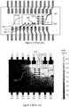
- FIG. 1 illustrates a conventional mixed-signal multi-chip component.
- Sensitive analog signals are carried between the MEMS die (100) and a digital IC die (200) over first bonding wires (101).
- the first bonding wires (101) are coupled to the dies (100, 200) at first chip pads (113).
- Digital signals are communicated from the digital IC die (200) towards outside circuitry via leads of a lead-frame, which is marked in the Figure 1 with diagonal striped fill.
- At least one digital signal is coupled from a second chip pad (205) to a bond pad of the lead-frame by second bonding wires (211).
- the bond pad is electrically connected to a lead configured to communicate with circuitry external of the mixed-signal multi-chip component using the at least one digital signal.
- Such bond pad carrying a digital signal may be a signal-bearing bond pad (202).
- Crosstalk may easily occur between a signal-bearing bond pad (202) and a first bonding wire (101) within the volume of the component body, since there is no electromagnetic interference (EMI) protection between the two.
- EMI electromagnetic interference
- the digital processing may not be able correct the erroneous results but assumes the voltage or current caused by crosstalk as being originally provided by the MEMS die (100).
- the digital signal does not represent properly the wanted signal comprising information received from the MEMS die (100), but it may be a sum of the wanted analog signal and crosstalk error.
- crosstalk reduces accuracy and reliability of detection results achieved with the MEMS device, which detection results are obtained by analysing the sensitive analog signals provided by the MEMS die (100) and carried by the first bonding wires (101).
- a sensitive analog signal carried by one of the first bonding wires (101) may be referred to as a victim or as a victim signal, whereas the disturbing digital signal carried through the second bonding wire (211) may be referred to as an aggressor and the signal-bearing bond pad (202) may also be referred to as an aggressor bond pad.
- the respective bonding wires may be referred to as a victim bonding wire (101) and an aggressor bonding wire (211).
- Figure 2 is a capture from a simulation that further illustrates the problem in the prior art.
- Electric potential caused by an aggressor bond pad (202) is illustrated with shades of grey. The whiter the area, the stronger is the voltage caused by the aggressor. In the black area the electric potential caused by the aggressor is not significant. While the victim bonding wires (101) carrying sensitive analog detection signals are all within the area at which the electric potential caused by the aggressor is high, risk of errors caused by crosstalk is significant.
- an exemplary test voltage of 1V was used in the aggressor bond pad (202). The resulting voltage caused by the aggressor bond pad at the area of the closest victim bonding wires (101) was found to be in the level of 5 mV.
- the actual amount of crosstalk and thus the error caused by the crosstalk at the victim bonding wires (101) depends on the nature and level of the aggressor and victim signals as well as various structural aspects of the design, but the simulation provides a good basis level for comparison.
- US Patent 6,538,336 discloses a semiconductor device assembly facilitating highspeed communication between an integrated circuit die and external circuitry. Signal-bearing bond pads are separated from one another by bond wires at fixed voltage levels.
- US patent 7,569,472 solves a problem of minimizing crosstalk between adjacent signal wires by introducing a power ring.
- US 8 921 955 B1 discloses a semiconductor device comprising a leadframe which includes a generally quadrangular die paddle or die pad. In addition to the die pad, the leadframe comprises a plurality of leads. The semiconductor device further comprises a MEMS die, the bottom surface of which is attached to the top surface of the die pad. In the semiconductor device, the MEMS die is electrically connected to the semiconductor die through the use of at least one conductive wire which extends from one of the bond pads of the MEMS die to a corresponding one of the bond pads of the semiconductor die.
- a solution is thus needed which reduces crosstalk between victim and aggressor signals communicated within a mixed-signal multi-chip MEMS package.
- An object is to provide a method and apparatus so as to solve the problem of crosstalk between digital and sensitive analog signals in a mixed-signal multi-chip package.
- the objects of the present invention are achieved with a mixed-signal multi-chip package according to the claim 1.
- the objects of the present invention are further achieved with a method according to the claim 7.
- the present invention is based on the idea of utilizing a combination of relative placement of the sensitive signals within the multi-chip component and the potentially disturbing outward signals, relative placements of bonding sites for outward signals as well as optimizing layout and size of the bonding sites for outward signals for reducing crosstalk between sensitive analog signals within the multi-chip design and digital signals communicated towards external circuitry.
- a mixed-signal multi-chip package comprising a lead frame, a first die and a digital die.
- the lead frame comprises a die handle.
- the first die attached to the die handle comprises MEMS structures and configured to provide at least one analog signal in at least one analog chip pad of the first die.
- the digital die attached to the die handle is configured to receive the at least one analog signal from the first die through at least one analog chip pad of the digital die, wherein a first bonding wire couples the at least one analog chip pad of the digital die with the respective at least one analog output chip pad of the first die.
- the at least one digital die is configured to communicate with external circuitry using at least one digital signal-bearing signal exchanged via at least one first bond pad of the lead-frame.
- At least one second bond pad of the lead frame configured to be coupled to a DC voltage extends laterally along a plane of the lead-frame between the at least one first bond pad and the first bonding wire, to form a DC guard between the at least one first bond pad and the first bonding wire.
- the area of the at least one first bond pad is less than 50% of the area of a median sized bond pad of the lead-frame.
- the at least one second bond pad is disposed adjacent to the at least one first bond pad at the side of the at least one first bond pad that is towards the first bonding wire.
- the at least one second bond pad covers a section of the circumference of the at least one first bond pad in the direction of the first wire bonding that is greater than a section of the circumference covered by an average size bond pad.
- the DC voltage is any one of a ground voltage and an operating voltage.
- the lead-frame comprises two second bond pads bridged by a bridging part of the lead frame with one another, wherein the at least one first bond pad resides between the two second bond pads, wherein the two second bond pads are short-circuited by the bridging part, wherein the bridging part encircles the at least one first bond pad at the side opposite of at least one signal-bearing lead configured to couple the respective at least one first bond pad towards external circuitry, and wherein the bridging part is configured to form an DC barrier between the at least one first bond pad and other of parts residing inside the mixed-signal multi-chip package.
- the bridging part is extended to further encircle a lateral area comprising the signal-bearing chip pads and the signal-bearing bonding wires coupling the at least one first bond pad and the signal-bearing chip pads.
- a method for reducing crosstalk in a mixed-signal multi-chip package comprising a lead frame comprising a die handle, the method comprising carrying at least one analog signal between at least one analog chip pad of a first die attached to the die handle, the first die comprising MEMS structures and at least one analog chip pad of at least one digital die attached to the die handle, wherein each of the at least one analog signal is carried between the respective analog chip pads by a first bonding wire, processing the at least one analog signal by circuitry of the digital die and communicating by the circuitry of the digital die with external circuitry using at least one digital signal-bearing signal exchanged via at least one first bond pad of a lead-frame.
- the method comprises coupling at least one second bond pad disposed between the at least one first bond pad and the first bonding wire to a DC voltage, wherein the at least one second bond pad extends laterally along a plane of the lead-frame to form a DC guard between the at least one first bond pad and the first bonding wire.
- the area of the at least one first bond pad is less than 50% of the area of a median sized bond pad of the lead-frame.
- the method further comprises disposing the at least one second bond pad adjacent to the at least one first bond pad at the side of the at least one first bond pad that is towards the first bonding wire.
- the method further comprises covering with the at least one second bond pad a section of the circumference of the at least one first bond pad in the direction of the first wire bonding that is greater than a section of the circumference covered by an average size bond pad.
- the DC voltage is any one of a ground voltage and an operating voltage.
- the method further comprises bridging, by a bridging part of the lead-frame, two second bond pads with one another, so that the at least one first bond pad resides between the two second bond pads.
- the two second bond pads are short-circuited by the bridging part.
- the bridging part encircles the at least one first bond pad at the side opposite of at least one signal-bearing lead configured to couple the respective at least one first bond pad towards external circuitry.
- the bridging part is configured to form an DC barrier between the at least one first bond pad and other of parts residing inside the mixed-signal multi-chip package.
- the method further comprises extending the bridging part to further encircle a lateral area of the package that comprises the signal-bearing chip pads and the signal-bearing bonding wires coupling the at least one first bond pad and the signal-bearing chip pads.
- the present invention has the advantage that the layout of the lead-frame may be optimized for minimized crosstalk with no additional cost, as long as the digital circuit layout allows the digital signal-bearing signals to be coupled to the lead-frame in a position that is away from the points of coupling the sensitive analog signals between the analog and digital dies
- Figures 1 to 7 show a top view of a multi-chip package, and dimensions along the illustrated plane (xy-plane) of this view may be referred to as the lateral dimensions.
- a MEMS die 100 comprises the electro-mechanical parts, which include moving elements, as well as analog circuitry configured at least to provide analog signals at chip pads (113) of the MEMS die (100).
- the chip pads (113) of the MEMS die (100) comprise at least analog output chip pads.
- the digital die (200) may be for example an application specific integrated circuit (ASIC) configured to receive analog signals from the MEMS die (100) over multiple first bonding wires 101 at the chip pads (113).
- ASIC application specific integrated circuit
- the chip pads (113) of the digital die (200) comprise at least analog input chip pads.
- the first bonding wires as the analog bonding wires (101), since they are used for carrying analog signals.
- analog signals received from a MEMS die (100) have relatively low current and/or voltage and are therefore sensitive to any electromagnetic interference.
- the analog signals carried by the first bonding wires (101) may be referred to as victims, since quality of these signals may suffer if exposed to any electromagnetic interference such as crosstalk.
- the MEMS die (100) and the digital die (200) may be attached to a die handle (140) for example by gluing.
- the die handle (140) which is part of the lead-frame, forms a mechanically rigid support for the dies (100, 200).
- the lateral area of the die handle (140) exceeds that of the dies (100, 200) attached to it.
- the MEMS die (100) and the digital die (200) are preferably designed and placed to facilitate short analog bonding wires (101) between the MEMS die (100) and the digital die (200).
- the analog bonding wires (101) attach to respective chip pads (113) of the MEMS die (100) and the digital die (200).
- the chip pads 113 of the MEMS die (100) for coupling the analog bonding wires (101) are arranged along one side of the MEMS die (100) and the chip pads (113) of the digital die (200) for coupling the analog bonding wires (101) are arranged along one side of the digital die (200) so that the orders of the chip pads (113) on the two dies correspond to each other so that the parallel analog bonding wires (101) form a row.
- Short analog bonding wires (101) contribute to improvement of the quality of sensitive analog signals communicated over the analog bonding wires (101) and reduce risk for unwanted electrical interference caused for example by crosstalk. Any wire bonding technology known in the art may be applied for the bonding the dies to each other and/or to the lead-frame.
- the digital die (200) communicates with external circuitry using digital signal-bearing signals. These digital signal-bearing signals are coupled from chip pads (205) of the digital die (200) by second bonding wires (201) to a plurality of bond pads (202) on the lead-frame of the multi-chip package. As these second bonding wires carry digital signal-bearing signals, we may call these signal-bearing bonding wires, and the respective chip pads (205) may be called signal-bearing chip pads. Likewise, the respective bond pads may be called signal-bearing bond pads (202). Ground and supply voltage signals for the digital die (200) are likewise connected between chip pads of the digital die (200) and a bond pad (212) of the lead-frame by bonding wires.
- the chip pads, bond pads and the bonding wires configured to carry the ground and supply voltage signals as DC chip pads (215), DC bonding wires (211) and DC bond pads (212).
- the signal-bearing bond pads (202) and the one or more DC bond pads (212) form part of a lead-frame of the component package, which comprises the bond pads and leads extending from the bond pads.
- Signal-bearing leads (232) are coupled to the signal-bearing bond pads (202) and DC leads (222) are coupled to the DC bond pads (212).
- Figures also show further bond pads (203) coupled to leads (213). These further bond pads (203) are shown as standard size reference bond pads.
- the further bond pads (203) may carry any signals.
- the chip pads (205, 215) are not all marked with reference signs in figure 2 for clarity but may be recognized in the figure 3 as small rectangular areas into which the thin bonding wires (101, 201, 211) are coupled to.
- the bond pads (202, 203, 212) form a plane.
- the die paddle (140) may reside in the same plane with the bond pads, or it may form another plane parallel with the plane of the bond pads.
- Bond pads (202, 203, 212) and die paddle (140) are disposed within the package body (150), while leads (213, 222, 232) extend outside the package body, facilitating coupling of the package for example to a printed circuit board (PCB).
- PCB printed circuit board
- a first aspect to notice is the relative placement of the signal-bearing chip pads, signal-bearing second bonding wires (201) and the signal-bearing bond pads (212).
- the signal-bearing chip pads (205) of the digital IC die are disposed in a location that is removed from the analog bonding wires (101).
- the signal-bearing chip pads are disposed essentially at or at least near a corner of the digital die (200), which corner is away from the analog bonding wires (101). If the multi-chip package had leads on all four sides, the signal-bearing chip pads could also be disposed along the side of the digital IC die (200) which is opposite to that of the chip pads (113) configured to carry the sensitive analog signals.
- the signals from the signal-bearing chip pads (205) are wire bonded to signal-bearing bond pads (202), which are located close to the signal-bearing chip pads to enable using short bonding wires (211).
- the signal-bearing bond pads (201) should also be disposed in a position on the lead-frame that is removed from the analog bonding wires (101).
- the mere distance between the possibly interfering digital signal-bearing elements facilitates reducing of crosstalk.
- short bonding wires reduce risk of crosstalk. This applies to all bonding wires, especially those carrying analog or digital signals.
- a second aspect is the size and design of the signal-bearing bond pads (202).
- the area of the signal-bearing bond pads (202) should be reduced or minimized. Minimizing refers to reducing the area as much as conveniently possible without compromising the capability to reliably attach of the bonding wire to the bond pad or compromising mechanical robustness of the lead-frame.
- the major part of the signal-bearing bond pads (202) comprises the area required for facilitating coupling the signal-bearing bond pad (202) towards the respective signal-bearing lead (232), but the area on the bond pads (202) reserved for attaching the bonding wire is preferably minimized, taking into account the design rules for the used bonding technology, component package requirements and lead-frame design requirements, which may set minimum allowed values for example for spacing between adjacent bond pads and width and length of bond pads for ensuring reliable bonding.
- the area of the signal-bearing bond pads (202) may be less than 50% of the area of other, "normal” or "median” bond pads (203).
- the area of the signal-bearing bond pads (202) is less than 50% of the area of a median sized bond pad (203) of the lead-frame.
- a third aspect is the location and the design of DC bond pads (212) and that of the respective DC chip pads (215).
- a DC bond pad (212) is disposed next to a signal-bearing bond pad (202) within area that is approximately between the signal-bearing bond pads (202) and the analog bonding wires (101).
- the DC chip pad (215) is preferably located near to the respective DC bond pad (212) and also in the immediate vicinity of the respective signal-bearing bond pad (205).
- Mere placement of the DC bond pad (212) facilitates reducing of crosstalk from the signal-bearing bond pads (202) towards the analog bonding wires (101). This effect can further be improved by designing the layout of the DC bond pad (212).
- the DC bond pad (212) which is adjacent to the signal-bearing bond pad (202) has been extended within the component package along a plane of the lead-frame so that it at least partially encircles the at least one signal-bearing bond pad (202), particularly at the side of the signal-bearing bond pad that resides towards the semiconductor dies.
- Partially encircling refers to a relative position of the DC bond pad (212) and the signal-bearing bond pad (202) in which the DC bond pad comprises an oblong part, for example a segment of an annulus, that covers a sector of circumference of the signal-bearing bond pad (202) that is greater than a sector covered by an average size bond pad disposed in the same location.
- the oblong part may be non-circular, i.e. it may have bends.
- the sector covered by the extended DC bond pad (212) resides in the direction of the victim bonding wire when looking from the aggressor, signal-bearing bond pad (202).
- the extended DC bond pad (212) thus forms a DC guard between the at least signal-bearing bond pad and the analog bonding wires (101).
- a DC guard can be characterized as a kind of guard trace between an aggressor and a victim such that a magnetic field created by the aggressor meets the DC guard so that a current induced by the magnetic field flows in the DC guard rather than in the victim.
- a DC signal, such as ground or an operating voltage is less sensitive to slight changes caused by such induced current.
- a special case of a DC guard is a ground guard, when the DC voltage is equal to the ground.
- other DC voltages such as an operating voltage may be used in a DC guard.
- the area of the extended DC bond pad (212) along the plane of the lead-frame is preferably greater than the area of a median sized "normal" or “average” bond pad (203).
- the extended DC bond pad (212) may carry ground or operating voltage, which are both DC signals that may be considered as electrical ground terminal in view of the digital signal-bearing signals carried through the signal-bearing bond pads (202).
- the extended layout of the DC bond pad (212) effectively forms a ground barrier between the possible interfering aggressor digital signal and the possible victim analog signals carried by the analog bonding wires (101).
- Figure 4 illustrates a simulation result of electromagnetic interference effects caused by one signal-bearing bond pad (202) along the lead-frame in the first embodiment of the figure 3 . Similar to the simulation plot of a prior art design shown in the figure 2 , white areas illustrate stronger electric potential caused by the signal-bearing bond pad (202) that represents an aggressor, while the black areas illustrate those areas in which the electric potential caused by the aggressor is low and risk of crosstalk is therefore significantly lower.
- the resulting voltage level caused by the aggressor in the area of the victim bonding wires (101) is in the level of 0-0.5mV, in other words, less than 10% of that of the reference layout shown in the figures 1 and 2 .
- the risk and level of error in the victim bonding wires (101) is to less than 10%.
- the level of crosstalk error in the signal in the multi-chip package design according to the first embodiment would also be reduced to less than 10% of that of the exemplary prior art multi-chip package design.
- FIGS 5, 6 and 7 illustrate further embodiments of the invention with alternative shapes of one or more extended DC bond pads (212).
- area of the DC bond pad (212) disposed next to the signal-bearing (aggressor) bond pad (202) is again bigger than any other bond pad in the lead-frame, and especially clearly bigger than that of the signal-bearing bond pads (212).
- the DC bond pad (212) is slightly extended so that the extension creates a DC guard between the aggressor and the possible victims.
- the cross-coupling protection caused by the extended DC bond pad (212) of the second embodiment is not as strong as in the first embodiment shown in the figure 3 , but the combined effect of relative placement of the DC bond pad (212) and the signal-bearing bond pads (202), small area of the signal-bearing bond pads (212) and maximized distance between the signal-bearing bonding wires (201) and bond pads (202) and the sensitive analog signal carrying bonding wires (101) may still provide sufficient level of protection from crosstalk.
- Figure 6 illustrates a third embodiment, in which the extended DC bond pad formed from the lead-frame is further extended along a plane of the lead-frame, so that it forms a bridging part (213).
- the bridging part (213) essentially encircles a signal-bearing bond pad (202) along a plane of the lead-frame at the side of the dies, in other words on the side opposite to the signal-bearing lead (232).
- This bridging part (213) bridges and short-circuits two extended DC bond pads (212), which may both be coupled to DC chip pads (215) with DC bonding wires (211).
- the bridging part (213) and the DC chip pads (215) preferably cover a sector of the circumference of the signal-bearing bond pad (202) that covers at least the half of the circumference of the signal-bearing bond pad (202) that resides opposite to the signal-bearing lead (232).
- the bridging part thus forms part of an annulus-like form in the plain of the lead-frame inside the component package, which form covers the sector between the two DC bond pads (212) short-circuited by the bridging part that resides opposite to the signal-bearing lead (232).
- the bringing part thus effectively creates a DC barrier between the signal-bearing bond pad (202) and the rest of the package, so that the DC barrier resides on the side of the signal-bearing bond pad (202) that is away from the signal-bearing lead (232).
- the DC barrier When coupled to ground potential, the DC barrier may also be called ground barrier.
- the DC barrier may also be coupled to another steady DC voltage, such as an operating voltage.
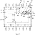
- Figure 7 illustrates a fourth embodiment, in which a bridging part (213) formed from the lead-frame around a plurality of signal-bearing bond pads 202. Similar to the embodiment of the figure 6 , this bridging part forms a DC barrier that short-circuits two DC bond pads (212), which may both be coupled to DC chip pads (215) with DC bonding wires (211).
- the bridging part (213) partially extends below the digital IC die (200), so that also the area in which the signal-bearing chip pads (205) are disposed resides on the side of the DC barrier that lies towards the signal-bearing leads (232), and so that the signal-bearing chip pads (205) are disposed at different side of the DC barrier than the possible victim bonding wires 101.
- the die handle (140) area has been reduced by removing one part of the die handle (140), thus leaving room for extending the bridging part (213).
- the configurations of figures 6 and 7 assumes that the two DC chip pads (215) short-circuited with each other shall be coupled to the same DC potential via the respective leads (222). Any number of signal-bearing bond pads (202) may be disposed behind the DC barrier formed by the bridging part (213) of embodiments of figures 6 and 7 . It is apparent to a person skilled in the art that as technology advanced, the basic idea of the invention can be implemented in various ways. The invention and its embodiments are therefore not restricted to the above examples, but they may vary within the scope of the claims.
Landscapes
- Engineering & Computer Science (AREA)
- Microelectronics & Electronic Packaging (AREA)
- Manufacturing & Machinery (AREA)
- Computer Hardware Design (AREA)
- Physics & Mathematics (AREA)
- Electromagnetism (AREA)
- Computer Networks & Wireless Communication (AREA)
- Signal Processing (AREA)
- Semiconductor Integrated Circuits (AREA)
- Wire Bonding (AREA)
Claims (12)
- Mischsignal-Multichipgehäuse umfassend:- einen Leadframe, der einen Die-Träger (140) umfasst,- einen ersten Die (100), der am Die-Träger angebracht ist und MEMS-Strukturen umfasst und dazu eingerichtet ist, mindestens ein analoges Signal in mindestens einem analogen Chip-Pad (113) des ersten Dies bereitzustellen, und- einen digitalen Die (200), der am Die-Träger angebracht ist und dazu eingerichtet ist, das mindestens eine analoge Signal vom ersten Die über mindestens ein analoges Chip-Pad (113) des digitalen Dies zu empfangen, wobei ein erster Bond-Draht (101) das mindestens eine analoge Chip-Pad des digitalen Dies mit dem entsprechenden mindestens einen analogen Output-Chip-Pad des ersten Dies koppelt,wobei der mindestens eine digitale Die (200) dazu eingerichtet ist, mit Hilfe mindestens eines digitalsignaltragenden Signals, das über mindestens ein erstes Bond-Pad (202) des Leadframes ausgetauscht wird, mit einer externen Schaltungsanordnung zu kommunizieren, und
wobei mindestens ein zweites Bond-Pad (212) des Leadframes, das für den Anschluss an eine Gleichspannung eingerichtet ist, sich seitlich entlang einer Ebene des Leadframes zwischen dem mindestens einen ersten Bond-Pad (202) und dem ersten Bond-Draht (101) erstreckt, um einen Gleichstromschutz zwischen dem mindestens einen ersten Bond-Pad und dem ersten Bond-Draht auszubilden,
dadurch gekennzeichnet, dass die Fläche des mindestens einen ersten Bond-Pads (202) weniger als 50 % der Fläche eines mittelgroßen Bond-Pads (203) des Leadframes beträgt. - Mischsignal-Multichipgehäuse nach Anspruch 1, wobei das mindestens eine zweite Bond-Pad (212) angrenzend zu dem mindestens einen ersten Bond-Pad (202) auf der zum ersten Bond-Draht (101) weisenden Seite des mindestens einen ersten Bond-Pads angeordnet ist.
- Mischsignal-Multichipgehäuse nach einem der Ansprüche 1 oder 2, wobei- das mindestens eine zweite Bond-Pad (212) einen in Richtung des ersten Bond-Drahts (101) liegenden Teilbereich des Umfangs des mindestens einen ersten Bond-Pads (202) bedeckt, der größer ist als ein durch ein durchschnittlich großes Bond-Pad (203) bedeckter Teilbereich des Umfangs.
- Mischsignal-Multichipgehäuse nach einem der Ansprüche 1 bis 3, wobei die Gleichspannung eine Massespannung oder eine Betriebsspannung ist.
- Mischsignal-Multichipgehäuse nach einem der Ansprüche 1 bis 4, wobei der Leadframe zwei zweite Bond-Pads (212) umfasst, die durch ein Brückenteil des Leadframes miteinander überbrückt sind, wobei das mindestens eine erste Bond-Pad (202) zwischen den beiden zweiten Bond-Pads (212) liegt, wobei die beiden zweiten Bond-Pads durch den Brückenteil kurzgeschlossen werden, wobei der Brückenteil das mindestens eine erste Bond-Pad auf der Seite umschließt, die entgegengesetzt zu der mindestens einen signaltragenden Leitung (232) ist, die dazu eingerichtet ist, das entsprechende mindestens eine erste Bond-Pad mit einer externen Schaltanordnung zu verbinden, und wobei der Brückenteil so eingerichtet ist, dass er eine Gleichstrombarriere zwischen dem mindestens einen ersten Bond-Pad (202) und anderen im Inneren des Mischsignal-Multichipgehäuses liegenden Teilen ausbildet.
- Mischsignal-Multichipgehäuse nach Anspruch 5, wobei der Brückenteil so verlängert ist, dass er ferner eine seitliche Fläche umschließt, die die signaltragenden Chip-Pads (205) und die signaltragenden Bond-Drähte (201), die das mindestens eine erste Bond-Pad (202) und die signaltragenden Chip-Pads (205) verbinden, umfasst.
- Verfahren zur Verminderung von Crosstalk in einem Mischsignal-Multichipgehäuse, das einen Leadframe umfasst, der einen Die-Träger (140) umfasst, wobei das Verfahren umfasst:- Führen mindestens eines analogen Signals zwischen mindestens einem analogen Chip-Pad (113) eines ersten Dies (100), der am Die-Träger angebracht ist und MEMS-Strukturen umfasst, und mindestens einem analogen Chip-Pad (113) mindestens eines am Die-Träger angebrachten digitalen Dies (200) umfasst, wobei das mindestens eine analoge Signal zwischen den entsprechenden analogen Chip-Pads durch einen ersten Bond-Draht (101) geführt wird;- Verarbeiten des mindestens einen analogen Signals durch eine Schaltungsanordnung des digitalen Dies (200);- Kommunizieren mit einer externen Schaltungsanordnung über die Schaltungsanordnung des digitalen Dies mit Hilfe mindestens eines digitalsignaltragenden Signals, das über mindestens ein erstes Bond-Pad (202) des Leadframes ausgetauscht wird; und- Verbinden mindestens eines zweiten Bond-Pads (212), das zwischen dem mindestens einen ersten Bond-Pad (202) und dem ersten Bond-Draht (101) angeordnet ist, mit einer Gleichspannung, wobei sich das mindestens eine zweite Bond-Pad (212) seitlich entlang einer Ebene des Leadframes erstreckt, um einen Gleichstromschutz zwischen dem mindestens einen ersten Bond-Pad (202) und dem ersten Bond-Draht (101) auszubilden,dadurch gekennzeichnet, dass die Fläche des mindestens ersten Bond-Pads (202) weniger als 50 % der Fläche eines mittelgroßen Bond-Pads (203) des Leadframes beträgt.
- Verfahren nach Anspruch 7, wobei das Verfahren ferner umfasst:
Anordnen des mindestens einen zweiten Bond-Pads (212) angrenzend zu dem mindestens einen ersten Bond-Pad (202) auf der zum ersten Bond-Draht (101) weisenden Seite des mindestens einen ersten Bond-Pads. - Verfahren nach einem der Ansprüche 7 oder 8, ferner umfassend:- Bedecken eines in Richtung des ersten Bond-Drahts (101) liegenden Teilbereichs des Umfangs des mindestens einen ersten Bond-Pads (202), der größer ist als ein durch ein durchschnittlich großes Bond-Pad (203) bedeckter Teilbereich des Umfangs, mit dem mindestens einen zweiten Bond-Pad (212).
- Verfahren nach einem der Ansprüche 7 bis 9, wobei die Gleichspannung eine Massespannung oder eine Betriebsspannung ist.
- Verfahren nach einem der Ansprüche 7 bis 10, ferner umfassend:- gegenseitiges Überbrücken von zwei zweiten Bond-Pads (212) durch einen Brückenteil des Leadframes, so dass das mindestens eine erste Bond-Pad (202) zwischen den beiden zweiten Bond-Pads (212) liegt, wobei die beiden zweiten Bond-Pads (212) durch den Brückenteil kurzgeschlossen werden, wobei der Brückenteil das mindestens eine erste Bond-Pad (202) auf der Seite umschließt, die entgegengesetzt zu der mindestens einen signaltragenden Leitung (232) ist, die dazu eingerichtet ist, das entsprechende mindestens eine erste Bond-Pad mit einer externen Schaltanordnung zu verbinden, und wobei der Brückenteil so eingerichtet ist, dass er eine Gleichstrombarriere zwischen dem mindestens einen ersten Bond-Pad (202) und anderen im Inneren des Mischsignal-Multichipgehäuses liegenden Teilen ausbildet.
- Verfahren nach Anspruch 11, wobei das Verfahren ferner umfasst:- Verlängern des Brückenteils, um ferner eine seitliche Fläche des Gehäuses zu umschließen, die die signaltragenden Chip-Pads (205) und die signaltragenden Bond-Drähte (201), die das mindestens eine erste Bond-Pad (202) und die signaltragenden Chip-Pads (205) verbinden, umfasst.
Priority Applications (1)
| Application Number | Priority Date | Filing Date | Title |
|---|---|---|---|
| EP20176768.8A EP3725737B1 (de) | 2018-05-22 | 2019-05-15 | Reduzierung des übersprechens in einem mixed-signal-multi-chip mems-gehäuse |
Applications Claiming Priority (1)
| Application Number | Priority Date | Filing Date | Title |
|---|---|---|---|
| FI20185469 | 2018-05-22 |
Related Child Applications (2)
| Application Number | Title | Priority Date | Filing Date |
|---|---|---|---|
| EP20176768.8A Division EP3725737B1 (de) | 2018-05-22 | 2019-05-15 | Reduzierung des übersprechens in einem mixed-signal-multi-chip mems-gehäuse |
| EP20176768.8A Division-Into EP3725737B1 (de) | 2018-05-22 | 2019-05-15 | Reduzierung des übersprechens in einem mixed-signal-multi-chip mems-gehäuse |
Publications (2)
| Publication Number | Publication Date |
|---|---|
| EP3575262A1 EP3575262A1 (de) | 2019-12-04 |
| EP3575262B1 true EP3575262B1 (de) | 2021-04-14 |
Family
ID=66589211
Family Applications (2)
| Application Number | Title | Priority Date | Filing Date |
|---|---|---|---|
| EP19174590.0A Active EP3575262B1 (de) | 2018-05-22 | 2019-05-15 | Reduzierung des übersprechens in einem mixed-signal mehrchip mems-vorrichtungsgehäuse |
| EP20176768.8A Active EP3725737B1 (de) | 2018-05-22 | 2019-05-15 | Reduzierung des übersprechens in einem mixed-signal-multi-chip mems-gehäuse |
Family Applications After (1)
| Application Number | Title | Priority Date | Filing Date |
|---|---|---|---|
| EP20176768.8A Active EP3725737B1 (de) | 2018-05-22 | 2019-05-15 | Reduzierung des übersprechens in einem mixed-signal-multi-chip mems-gehäuse |
Country Status (4)
| Country | Link |
|---|---|
| US (1) | US10633246B2 (de) |
| EP (2) | EP3575262B1 (de) |
| JP (1) | JP6806185B2 (de) |
| CN (1) | CN110510571B (de) |
Families Citing this family (4)
| Publication number | Priority date | Publication date | Assignee | Title |
|---|---|---|---|---|
| TWI770618B (zh) * | 2020-09-26 | 2022-07-11 | 矽品精密工業股份有限公司 | 電子封裝件及其承載基板 |
| US11063629B1 (en) * | 2020-10-14 | 2021-07-13 | Nvidia Corporation | Techniques for detecting wireless communications interference from a wired communications channel |
| TWI737529B (zh) * | 2020-10-30 | 2021-08-21 | 精拓科技股份有限公司 | 數位隔離器 |
| US20230092132A1 (en) * | 2021-09-23 | 2023-03-23 | Texas Instruments Incorporated | Wafer level processing for microelectronic device package with cavity |
Family Cites Families (35)
| Publication number | Priority date | Publication date | Assignee | Title |
|---|---|---|---|---|
| US5511428A (en) * | 1994-06-10 | 1996-04-30 | Massachusetts Institute Of Technology | Backside contact of sensor microstructures |
| JPH0870090A (ja) * | 1994-08-30 | 1996-03-12 | Kawasaki Steel Corp | 半導体集積回路 |
| JP3106087B2 (ja) * | 1995-04-07 | 2000-11-06 | 松下電器産業株式会社 | リードフレーム及び半導体装置 |
| US6538336B1 (en) | 2000-11-14 | 2003-03-25 | Rambus Inc. | Wirebond assembly for high-speed integrated circuits |
| JP2003204027A (ja) * | 2002-01-09 | 2003-07-18 | Matsushita Electric Ind Co Ltd | リードフレーム及びその製造方法、樹脂封止型半導体装置及びその製造方法 |
| JP4146290B2 (ja) * | 2003-06-06 | 2008-09-10 | 株式会社ルネサステクノロジ | 半導体装置 |
| US7064442B1 (en) * | 2003-07-02 | 2006-06-20 | Analog Devices, Inc. | Integrated circuit package device |
| US7557433B2 (en) * | 2004-10-25 | 2009-07-07 | Mccain Joseph H | Microelectronic device with integrated energy source |
| US6933599B2 (en) * | 2003-10-27 | 2005-08-23 | Freescale Semiconductor, Inc. | Electromagnetic noise shielding in semiconductor packages using caged interconnect structures |
| US20050205951A1 (en) * | 2004-03-18 | 2005-09-22 | Honeywell Internatioanl, Inc. | Flip chip bonded micro-electromechanical system (MEMS) device |
| US8003443B2 (en) * | 2006-03-10 | 2011-08-23 | Stats Chippac Ltd. | Non-leaded integrated circuit package system with multiple ground sites |
| WO2007127348A2 (en) * | 2006-04-26 | 2007-11-08 | Ems Technologies, Inc. | Planar mixed-signal circuit board |
| US7569472B2 (en) | 2006-10-31 | 2009-08-04 | Lsi Corporation | Method and apparatus of power ring positioning to minimize crosstalk |
| US7843021B2 (en) * | 2008-02-28 | 2010-11-30 | Shandong Gettop Acoustic Co. Ltd. | Double-side mountable MEMS package |
| US8154134B2 (en) * | 2008-05-12 | 2012-04-10 | Texas Instruments Incorporated | Packaged electronic devices with face-up die having TSV connection to leads and die pad |
| JP5191915B2 (ja) * | 2009-01-30 | 2013-05-08 | ルネサスエレクトロニクス株式会社 | 半導体装置およびその製造方法 |
| SG175784A1 (en) * | 2009-04-27 | 2011-12-29 | Vitae Pte Ltd E | On-chip laboratory for blood analysis |
| US8217474B2 (en) * | 2009-12-28 | 2012-07-10 | Solid State System Co., Ltd. | Hermetic MEMS device and method for fabricating hermetic MEMS device and package structure of MEMS device |
| WO2011092980A1 (ja) * | 2010-01-28 | 2011-08-04 | 株式会社村田製作所 | 可変容量装置 |
| US8618620B2 (en) * | 2010-07-13 | 2013-12-31 | Infineon Technologies Ag | Pressure sensor package systems and methods |
| US8921955B1 (en) * | 2011-02-24 | 2014-12-30 | Amkor Technology, Inc. | Semiconductor device with micro electromechanical system die |
| ITAN20110029A1 (it) * | 2011-03-01 | 2012-09-02 | Stefano Marchetti | Sistema integrato di tele-alimentazione per trasmissioni bidirezionali a larga banda |
| JP5618873B2 (ja) * | 2011-03-15 | 2014-11-05 | ルネサスエレクトロニクス株式会社 | 半導体装置の製造方法 |
| US8674486B2 (en) * | 2011-12-14 | 2014-03-18 | Samsung Electro-Mechanics | Isolation barrier device and methods of use |
| KR102071078B1 (ko) * | 2012-12-06 | 2020-01-30 | 매그나칩 반도체 유한회사 | 멀티 칩 패키지 |
| JP2015095486A (ja) * | 2013-11-08 | 2015-05-18 | アイシン精機株式会社 | 半導体装置 |
| EP3128544B1 (de) * | 2014-04-03 | 2021-01-20 | Murata Manufacturing Co., Ltd. | Vorrichtung mit variabler kapazität und herstellungsverfahren dafür |
| US9905410B2 (en) * | 2015-01-31 | 2018-02-27 | Agilent Technologies, Inc. | Time-of-flight mass spectrometry using multi-channel detectors |
| JP6522402B2 (ja) * | 2015-04-16 | 2019-05-29 | ローム株式会社 | 半導体装置 |
| US10333505B2 (en) * | 2017-02-21 | 2019-06-25 | M31 Technology Corporation | Repetitive IO structure in a PHY for supporting C-PHY compatible standard and/or D-PHY compatible standard |
| EP3470366B1 (de) * | 2017-10-12 | 2020-07-08 | Murata Manufacturing Co., Ltd. | Reduzierung von vibration einer mems installation auf einer leiterplatte |
| DE102018106560B4 (de) * | 2017-10-17 | 2025-01-02 | Infineon Technologies Ag | Drucksensorbauelemente und Verfahren zum Herstellen von Drucksensorbauelementen |
| US10566301B2 (en) * | 2017-11-17 | 2020-02-18 | General Electric Company | Semiconductor logic device and system and method of embedded packaging of same |
| US10396053B2 (en) * | 2017-11-17 | 2019-08-27 | General Electric Company | Semiconductor logic device and system and method of embedded packaging of same |
| JP2019165197A (ja) * | 2017-12-13 | 2019-09-26 | 株式会社村田製作所 | 半導体部品のemc保護 |
-
2019
- 2019-05-15 EP EP19174590.0A patent/EP3575262B1/de active Active
- 2019-05-15 EP EP20176768.8A patent/EP3725737B1/de active Active
- 2019-05-21 CN CN201910424132.XA patent/CN110510571B/zh active Active
- 2019-05-22 US US16/419,453 patent/US10633246B2/en active Active
- 2019-05-22 JP JP2019095767A patent/JP6806185B2/ja active Active
Non-Patent Citations (1)
| Title |
|---|
| None * |
Also Published As
| Publication number | Publication date |
|---|---|
| US10633246B2 (en) | 2020-04-28 |
| EP3575262A1 (de) | 2019-12-04 |
| CN110510571B (zh) | 2023-07-25 |
| US20190359480A1 (en) | 2019-11-28 |
| CN110510571A (zh) | 2019-11-29 |
| EP3725737A1 (de) | 2020-10-21 |
| EP3725737B1 (de) | 2023-07-26 |
| JP6806185B2 (ja) | 2021-01-06 |
| JP2019216237A (ja) | 2019-12-19 |
Similar Documents
| Publication | Publication Date | Title |
|---|---|---|
| EP3725737B1 (de) | Reduzierung des übersprechens in einem mixed-signal-multi-chip mems-gehäuse | |
| US4647148A (en) | Fiber optic receiver module | |
| US9760754B2 (en) | Printed circuit board assembly forming enhanced fingerprint module | |
| EP0810655A2 (de) | Eine Packung für eine Halbleiteranordnung | |
| US8330236B2 (en) | Isolation channel improving measurement accuracy of MEMS devices | |
| EP2757812A1 (de) | Halbleitervorrichtung und mikrofon | |
| US6962081B2 (en) | Semiconductor physical quantity sensor with improved noise resistance | |
| KR100487038B1 (ko) | 반도체 디바이스 | |
| US20200266151A1 (en) | Electronic package structure | |
| EP3499566A1 (de) | Emv-schutz eines halbleiterbauelements | |
| KR100652106B1 (ko) | 회로 장치 | |
| KR100576302B1 (ko) | 반도체장치 | |
| US20070277607A1 (en) | Semiconductor acceleration sensor | |
| US5719748A (en) | Semiconductor package with a bridge for chip area connection | |
| CN212387732U (zh) | 电子设备 | |
| JP2002299568A (ja) | Icチップ | |
| KR101103772B1 (ko) | 일체형 모션 캡처용 6축 센서 및 그 제조 방법 | |
| CN114930138A (zh) | 力传感器 | |
| KR100945501B1 (ko) | 반도체 패키지 | |
| JP2006153724A (ja) | 加速度センサモジュール | |
| JP4923937B2 (ja) | センサ装置 | |
| JP2005516377A (ja) | 集積回路センサのための改善された接続組立体 | |
| CN106548995B (zh) | 电路板模块及其半导体封装件 | |
| KR101752056B1 (ko) | Mems 패키지 | |
| US20070096314A1 (en) | Semiconductor device and manufacturing method thereof |
Legal Events
| Date | Code | Title | Description |
|---|---|---|---|
| PUAI | Public reference made under article 153(3) epc to a published international application that has entered the european phase |
Free format text: ORIGINAL CODE: 0009012 |
|
| STAA | Information on the status of an ep patent application or granted ep patent |
Free format text: STATUS: REQUEST FOR EXAMINATION WAS MADE |
|
| 17P | Request for examination filed |
Effective date: 20190515 |
|
| AK | Designated contracting states |
Kind code of ref document: A1 Designated state(s): AL AT BE BG CH CY CZ DE DK EE ES FI FR GB GR HR HU IE IS IT LI LT LU LV MC MK MT NL NO PL PT RO RS SE SI SK SM TR |
|
| AX | Request for extension of the european patent |
Extension state: BA ME |
|
| GRAP | Despatch of communication of intention to grant a patent |
Free format text: ORIGINAL CODE: EPIDOSNIGR1 |
|
| STAA | Information on the status of an ep patent application or granted ep patent |
Free format text: STATUS: GRANT OF PATENT IS INTENDED |
|
| INTG | Intention to grant announced |
Effective date: 20201109 |
|
| GRAS | Grant fee paid |
Free format text: ORIGINAL CODE: EPIDOSNIGR3 |
|
| GRAA | (expected) grant |
Free format text: ORIGINAL CODE: 0009210 |
|
| STAA | Information on the status of an ep patent application or granted ep patent |
Free format text: STATUS: THE PATENT HAS BEEN GRANTED |
|
| AK | Designated contracting states |
Kind code of ref document: B1 Designated state(s): AL AT BE BG CH CY CZ DE DK EE ES FI FR GB GR HR HU IE IS IT LI LT LU LV MC MK MT NL NO PL PT RO RS SE SI SK SM TR |
|
| REG | Reference to a national code |
Ref country code: GB Ref legal event code: FG4D |
|
| REG | Reference to a national code |
Ref country code: CH Ref legal event code: EP |
|
| REG | Reference to a national code |
Ref country code: DE Ref legal event code: R096 Ref document number: 602019003834 Country of ref document: DE |
|
| REG | Reference to a national code |
Ref country code: IE Ref legal event code: FG4D |
|
| REG | Reference to a national code |
Ref country code: AT Ref legal event code: REF Ref document number: 1382223 Country of ref document: AT Kind code of ref document: T Effective date: 20210515 |
|
| REG | Reference to a national code |
Ref country code: LT Ref legal event code: MG9D |
|
| REG | Reference to a national code |
Ref country code: AT Ref legal event code: MK05 Ref document number: 1382223 Country of ref document: AT Kind code of ref document: T Effective date: 20210414 |
|
| REG | Reference to a national code |
Ref country code: NL Ref legal event code: MP Effective date: 20210414 |
|
| PG25 | Lapsed in a contracting state [announced via postgrant information from national office to epo] |
Ref country code: AT Free format text: LAPSE BECAUSE OF FAILURE TO SUBMIT A TRANSLATION OF THE DESCRIPTION OR TO PAY THE FEE WITHIN THE PRESCRIBED TIME-LIMIT Effective date: 20210414 Ref country code: BG Free format text: LAPSE BECAUSE OF FAILURE TO SUBMIT A TRANSLATION OF THE DESCRIPTION OR TO PAY THE FEE WITHIN THE PRESCRIBED TIME-LIMIT Effective date: 20210714 Ref country code: NL Free format text: LAPSE BECAUSE OF FAILURE TO SUBMIT A TRANSLATION OF THE DESCRIPTION OR TO PAY THE FEE WITHIN THE PRESCRIBED TIME-LIMIT Effective date: 20210414 Ref country code: FI Free format text: LAPSE BECAUSE OF FAILURE TO SUBMIT A TRANSLATION OF THE DESCRIPTION OR TO PAY THE FEE WITHIN THE PRESCRIBED TIME-LIMIT Effective date: 20210414 Ref country code: HR Free format text: LAPSE BECAUSE OF FAILURE TO SUBMIT A TRANSLATION OF THE DESCRIPTION OR TO PAY THE FEE WITHIN THE PRESCRIBED TIME-LIMIT Effective date: 20210414 Ref country code: LT Free format text: LAPSE BECAUSE OF FAILURE TO SUBMIT A TRANSLATION OF THE DESCRIPTION OR TO PAY THE FEE WITHIN THE PRESCRIBED TIME-LIMIT Effective date: 20210414 |
|
| PG25 | Lapsed in a contracting state [announced via postgrant information from national office to epo] |
Ref country code: LV Free format text: LAPSE BECAUSE OF FAILURE TO SUBMIT A TRANSLATION OF THE DESCRIPTION OR TO PAY THE FEE WITHIN THE PRESCRIBED TIME-LIMIT Effective date: 20210414 Ref country code: PL Free format text: LAPSE BECAUSE OF FAILURE TO SUBMIT A TRANSLATION OF THE DESCRIPTION OR TO PAY THE FEE WITHIN THE PRESCRIBED TIME-LIMIT Effective date: 20210414 Ref country code: NO Free format text: LAPSE BECAUSE OF FAILURE TO SUBMIT A TRANSLATION OF THE DESCRIPTION OR TO PAY THE FEE WITHIN THE PRESCRIBED TIME-LIMIT Effective date: 20210714 Ref country code: PT Free format text: LAPSE BECAUSE OF FAILURE TO SUBMIT A TRANSLATION OF THE DESCRIPTION OR TO PAY THE FEE WITHIN THE PRESCRIBED TIME-LIMIT Effective date: 20210816 Ref country code: RS Free format text: LAPSE BECAUSE OF FAILURE TO SUBMIT A TRANSLATION OF THE DESCRIPTION OR TO PAY THE FEE WITHIN THE PRESCRIBED TIME-LIMIT Effective date: 20210414 Ref country code: SE Free format text: LAPSE BECAUSE OF FAILURE TO SUBMIT A TRANSLATION OF THE DESCRIPTION OR TO PAY THE FEE WITHIN THE PRESCRIBED TIME-LIMIT Effective date: 20210414 Ref country code: IS Free format text: LAPSE BECAUSE OF FAILURE TO SUBMIT A TRANSLATION OF THE DESCRIPTION OR TO PAY THE FEE WITHIN THE PRESCRIBED TIME-LIMIT Effective date: 20210814 Ref country code: GR Free format text: LAPSE BECAUSE OF FAILURE TO SUBMIT A TRANSLATION OF THE DESCRIPTION OR TO PAY THE FEE WITHIN THE PRESCRIBED TIME-LIMIT Effective date: 20210715 |
|
| REG | Reference to a national code |
Ref country code: DE Ref legal event code: R097 Ref document number: 602019003834 Country of ref document: DE |
|
| PG25 | Lapsed in a contracting state [announced via postgrant information from national office to epo] |
Ref country code: SM Free format text: LAPSE BECAUSE OF FAILURE TO SUBMIT A TRANSLATION OF THE DESCRIPTION OR TO PAY THE FEE WITHIN THE PRESCRIBED TIME-LIMIT Effective date: 20210414 Ref country code: RO Free format text: LAPSE BECAUSE OF FAILURE TO SUBMIT A TRANSLATION OF THE DESCRIPTION OR TO PAY THE FEE WITHIN THE PRESCRIBED TIME-LIMIT Effective date: 20210414 Ref country code: MC Free format text: LAPSE BECAUSE OF FAILURE TO SUBMIT A TRANSLATION OF THE DESCRIPTION OR TO PAY THE FEE WITHIN THE PRESCRIBED TIME-LIMIT Effective date: 20210414 Ref country code: DK Free format text: LAPSE BECAUSE OF FAILURE TO SUBMIT A TRANSLATION OF THE DESCRIPTION OR TO PAY THE FEE WITHIN THE PRESCRIBED TIME-LIMIT Effective date: 20210414 Ref country code: CZ Free format text: LAPSE BECAUSE OF FAILURE TO SUBMIT A TRANSLATION OF THE DESCRIPTION OR TO PAY THE FEE WITHIN THE PRESCRIBED TIME-LIMIT Effective date: 20210414 Ref country code: LU Free format text: LAPSE BECAUSE OF NON-PAYMENT OF DUE FEES Effective date: 20210515 Ref country code: SK Free format text: LAPSE BECAUSE OF FAILURE TO SUBMIT A TRANSLATION OF THE DESCRIPTION OR TO PAY THE FEE WITHIN THE PRESCRIBED TIME-LIMIT Effective date: 20210414 Ref country code: EE Free format text: LAPSE BECAUSE OF FAILURE TO SUBMIT A TRANSLATION OF THE DESCRIPTION OR TO PAY THE FEE WITHIN THE PRESCRIBED TIME-LIMIT Effective date: 20210414 Ref country code: ES Free format text: LAPSE BECAUSE OF FAILURE TO SUBMIT A TRANSLATION OF THE DESCRIPTION OR TO PAY THE FEE WITHIN THE PRESCRIBED TIME-LIMIT Effective date: 20210414 |
|
| REG | Reference to a national code |
Ref country code: BE Ref legal event code: MM Effective date: 20210531 |
|
| PLBE | No opposition filed within time limit |
Free format text: ORIGINAL CODE: 0009261 |
|
| STAA | Information on the status of an ep patent application or granted ep patent |
Free format text: STATUS: NO OPPOSITION FILED WITHIN TIME LIMIT |
|
| 26N | No opposition filed |
Effective date: 20220117 |
|
| PG25 | Lapsed in a contracting state [announced via postgrant information from national office to epo] |
Ref country code: IE Free format text: LAPSE BECAUSE OF NON-PAYMENT OF DUE FEES Effective date: 20210515 |
|
| PG25 | Lapsed in a contracting state [announced via postgrant information from national office to epo] |
Ref country code: IS Free format text: LAPSE BECAUSE OF FAILURE TO SUBMIT A TRANSLATION OF THE DESCRIPTION OR TO PAY THE FEE WITHIN THE PRESCRIBED TIME-LIMIT Effective date: 20210814 Ref country code: AL Free format text: LAPSE BECAUSE OF FAILURE TO SUBMIT A TRANSLATION OF THE DESCRIPTION OR TO PAY THE FEE WITHIN THE PRESCRIBED TIME-LIMIT Effective date: 20210414 |
|
| PG25 | Lapsed in a contracting state [announced via postgrant information from national office to epo] |
Ref country code: BE Free format text: LAPSE BECAUSE OF NON-PAYMENT OF DUE FEES Effective date: 20210531 |
|
| REG | Reference to a national code |
Ref country code: CH Ref legal event code: PL |
|
| PG25 | Lapsed in a contracting state [announced via postgrant information from national office to epo] |
Ref country code: LI Free format text: LAPSE BECAUSE OF NON-PAYMENT OF DUE FEES Effective date: 20220531 Ref country code: CH Free format text: LAPSE BECAUSE OF NON-PAYMENT OF DUE FEES Effective date: 20220531 |
|
| PG25 | Lapsed in a contracting state [announced via postgrant information from national office to epo] |
Ref country code: CY Free format text: LAPSE BECAUSE OF FAILURE TO SUBMIT A TRANSLATION OF THE DESCRIPTION OR TO PAY THE FEE WITHIN THE PRESCRIBED TIME-LIMIT Effective date: 20210414 |
|
| PG25 | Lapsed in a contracting state [announced via postgrant information from national office to epo] |
Ref country code: HU Free format text: LAPSE BECAUSE OF FAILURE TO SUBMIT A TRANSLATION OF THE DESCRIPTION OR TO PAY THE FEE WITHIN THE PRESCRIBED TIME-LIMIT; INVALID AB INITIO Effective date: 20190515 |
|
| GBPC | Gb: european patent ceased through non-payment of renewal fee |
Effective date: 20230515 |
|
| PG25 | Lapsed in a contracting state [announced via postgrant information from national office to epo] |
Ref country code: MK Free format text: LAPSE BECAUSE OF FAILURE TO SUBMIT A TRANSLATION OF THE DESCRIPTION OR TO PAY THE FEE WITHIN THE PRESCRIBED TIME-LIMIT Effective date: 20210414 Ref country code: GB Free format text: LAPSE BECAUSE OF NON-PAYMENT OF DUE FEES Effective date: 20230515 |
|
| PG25 | Lapsed in a contracting state [announced via postgrant information from national office to epo] |
Ref country code: MT Free format text: LAPSE BECAUSE OF FAILURE TO SUBMIT A TRANSLATION OF THE DESCRIPTION OR TO PAY THE FEE WITHIN THE PRESCRIBED TIME-LIMIT Effective date: 20210414 |
|
| PGFP | Annual fee paid to national office [announced via postgrant information from national office to epo] |
Ref country code: DE Payment date: 20250521 Year of fee payment: 7 |
|
| PGFP | Annual fee paid to national office [announced via postgrant information from national office to epo] |
Ref country code: IT Payment date: 20250527 Year of fee payment: 7 |
|
| PGFP | Annual fee paid to national office [announced via postgrant information from national office to epo] |
Ref country code: FR Payment date: 20250528 Year of fee payment: 7 |
|
| PG25 | Lapsed in a contracting state [announced via postgrant information from national office to epo] |
Ref country code: TR Free format text: LAPSE BECAUSE OF FAILURE TO SUBMIT A TRANSLATION OF THE DESCRIPTION OR TO PAY THE FEE WITHIN THE PRESCRIBED TIME-LIMIT Effective date: 20210414 |