EP3559975B1 - Generative fertigung von dreidimensionalen artikeln - Google Patents
Generative fertigung von dreidimensionalen artikeln Download PDFInfo
- Publication number
- EP3559975B1 EP3559975B1 EP17808796.1A EP17808796A EP3559975B1 EP 3559975 B1 EP3559975 B1 EP 3559975B1 EP 17808796 A EP17808796 A EP 17808796A EP 3559975 B1 EP3559975 B1 EP 3559975B1
- Authority
- EP
- European Patent Office
- Prior art keywords
- cathode
- negative
- anode
- electron beam
- cup
- Prior art date
- Legal status (The legal status is an assumption and is not a legal conclusion. Google has not performed a legal analysis and makes no representation as to the accuracy of the status listed.)
- Active
Links
Images


Classifications
-
- H—ELECTRICITY
- H01—ELECTRIC ELEMENTS
- H01J—ELECTRIC DISCHARGE TUBES OR DISCHARGE LAMPS
- H01J3/00—Details of electron-optical or ion-optical arrangements or of ion traps common to two or more basic types of discharge tubes or lamps
- H01J3/02—Electron guns
-
- B—PERFORMING OPERATIONS; TRANSPORTING
- B22—CASTING; POWDER METALLURGY
- B22F—WORKING METALLIC POWDER; MANUFACTURE OF ARTICLES FROM METALLIC POWDER; MAKING METALLIC POWDER; APPARATUS OR DEVICES SPECIALLY ADAPTED FOR METALLIC POWDER
- B22F10/00—Additive manufacturing of workpieces or articles from metallic powder
- B22F10/20—Direct sintering or melting
- B22F10/28—Powder bed fusion, e.g. selective laser melting [SLM] or electron beam melting [EBM]
-
- B—PERFORMING OPERATIONS; TRANSPORTING
- B22—CASTING; POWDER METALLURGY
- B22F—WORKING METALLIC POWDER; MANUFACTURE OF ARTICLES FROM METALLIC POWDER; MAKING METALLIC POWDER; APPARATUS OR DEVICES SPECIALLY ADAPTED FOR METALLIC POWDER
- B22F12/00—Apparatus or devices specially adapted for additive manufacturing; Auxiliary means for additive manufacturing; Combinations of additive manufacturing apparatus or devices with other processing apparatus or devices
- B22F12/40—Radiation means
- B22F12/41—Radiation means characterised by the type, e.g. laser or electron beam
-
- B—PERFORMING OPERATIONS; TRANSPORTING
- B22—CASTING; POWDER METALLURGY
- B22F—WORKING METALLIC POWDER; MANUFACTURE OF ARTICLES FROM METALLIC POWDER; MAKING METALLIC POWDER; APPARATUS OR DEVICES SPECIALLY ADAPTED FOR METALLIC POWDER
- B22F12/00—Apparatus or devices specially adapted for additive manufacturing; Auxiliary means for additive manufacturing; Combinations of additive manufacturing apparatus or devices with other processing apparatus or devices
- B22F12/90—Means for process control, e.g. cameras or sensors
-
- B—PERFORMING OPERATIONS; TRANSPORTING
- B22—CASTING; POWDER METALLURGY
- B22F—WORKING METALLIC POWDER; MANUFACTURE OF ARTICLES FROM METALLIC POWDER; MAKING METALLIC POWDER; APPARATUS OR DEVICES SPECIALLY ADAPTED FOR METALLIC POWDER
- B22F7/00—Manufacture of composite layers, workpieces, or articles, comprising metallic powder, by sintering the powder, with or without compacting wherein at least one part is obtained by sintering or compression
- B22F7/06—Manufacture of composite layers, workpieces, or articles, comprising metallic powder, by sintering the powder, with or without compacting wherein at least one part is obtained by sintering or compression of composite workpieces or articles from parts, e.g. to form tipped tools
-
- B—PERFORMING OPERATIONS; TRANSPORTING
- B23—MACHINE TOOLS; METAL-WORKING NOT OTHERWISE PROVIDED FOR
- B23K—SOLDERING OR UNSOLDERING; WELDING; CLADDING OR PLATING BY SOLDERING OR WELDING; CUTTING BY APPLYING HEAT LOCALLY, e.g. FLAME CUTTING; WORKING BY LASER BEAM
- B23K15/00—Electron-beam welding or cutting
- B23K15/0046—Welding
- B23K15/0086—Welding welding for purposes other than joining, e.g. built-up welding
-
- B—PERFORMING OPERATIONS; TRANSPORTING
- B23—MACHINE TOOLS; METAL-WORKING NOT OTHERWISE PROVIDED FOR
- B23K—SOLDERING OR UNSOLDERING; WELDING; CLADDING OR PLATING BY SOLDERING OR WELDING; CUTTING BY APPLYING HEAT LOCALLY, e.g. FLAME CUTTING; WORKING BY LASER BEAM
- B23K15/00—Electron-beam welding or cutting
- B23K15/02—Control circuits therefor
-
- B—PERFORMING OPERATIONS; TRANSPORTING
- B23—MACHINE TOOLS; METAL-WORKING NOT OTHERWISE PROVIDED FOR
- B23K—SOLDERING OR UNSOLDERING; WELDING; CLADDING OR PLATING BY SOLDERING OR WELDING; CUTTING BY APPLYING HEAT LOCALLY, e.g. FLAME CUTTING; WORKING BY LASER BEAM
- B23K15/00—Electron-beam welding or cutting
- B23K15/06—Electron-beam welding or cutting within a vacuum chamber
-
- B—PERFORMING OPERATIONS; TRANSPORTING
- B28—WORKING CEMENT, CLAY, OR STONE
- B28B—SHAPING CLAY OR OTHER CERAMIC COMPOSITIONS; SHAPING SLAG; SHAPING MIXTURES CONTAINING CEMENTITIOUS MATERIAL, e.g. PLASTER
- B28B1/00—Producing shaped prefabricated articles from the material
- B28B1/001—Rapid manufacturing of 3D objects by additive depositing, agglomerating or laminating of material
-
- B—PERFORMING OPERATIONS; TRANSPORTING
- B28—WORKING CEMENT, CLAY, OR STONE
- B28B—SHAPING CLAY OR OTHER CERAMIC COMPOSITIONS; SHAPING SLAG; SHAPING MIXTURES CONTAINING CEMENTITIOUS MATERIAL, e.g. PLASTER
- B28B17/00—Details of, or accessories for, apparatus for shaping the material; Auxiliary measures taken in connection with such shaping
- B28B17/0063—Control arrangements
- B28B17/0081—Process control
-
- B—PERFORMING OPERATIONS; TRANSPORTING
- B29—WORKING OF PLASTICS; WORKING OF SUBSTANCES IN A PLASTIC STATE IN GENERAL
- B29C—SHAPING OR JOINING OF PLASTICS; SHAPING OF MATERIAL IN A PLASTIC STATE, NOT OTHERWISE PROVIDED FOR; AFTER-TREATMENT OF THE SHAPED PRODUCTS, e.g. REPAIRING
- B29C64/00—Additive manufacturing, i.e. manufacturing of three-dimensional [3D] objects by additive deposition, additive agglomeration or additive layering, e.g. by 3D printing, stereolithography or selective laser sintering
- B29C64/10—Processes of additive manufacturing
- B29C64/141—Processes of additive manufacturing using only solid materials
- B29C64/153—Processes of additive manufacturing using only solid materials using layers of powder being selectively joined, e.g. by selective laser sintering or melting
-
- B—PERFORMING OPERATIONS; TRANSPORTING
- B29—WORKING OF PLASTICS; WORKING OF SUBSTANCES IN A PLASTIC STATE IN GENERAL
- B29C—SHAPING OR JOINING OF PLASTICS; SHAPING OF MATERIAL IN A PLASTIC STATE, NOT OTHERWISE PROVIDED FOR; AFTER-TREATMENT OF THE SHAPED PRODUCTS, e.g. REPAIRING
- B29C64/00—Additive manufacturing, i.e. manufacturing of three-dimensional [3D] objects by additive deposition, additive agglomeration or additive layering, e.g. by 3D printing, stereolithography or selective laser sintering
- B29C64/20—Apparatus for additive manufacturing; Details thereof or accessories therefor
- B29C64/264—Arrangements for irradiation
- B29C64/268—Arrangements for irradiation using laser beams; using electron beams [EB]
-
- B—PERFORMING OPERATIONS; TRANSPORTING
- B33—ADDITIVE MANUFACTURING TECHNOLOGY
- B33Y—ADDITIVE MANUFACTURING, i.e. MANUFACTURING OF THREE-DIMENSIONAL [3-D] OBJECTS BY ADDITIVE DEPOSITION, ADDITIVE AGGLOMERATION OR ADDITIVE LAYERING, e.g. BY 3-D PRINTING, STEREOLITHOGRAPHY OR SELECTIVE LASER SINTERING
- B33Y10/00—Processes of additive manufacturing
-
- B—PERFORMING OPERATIONS; TRANSPORTING
- B33—ADDITIVE MANUFACTURING TECHNOLOGY
- B33Y—ADDITIVE MANUFACTURING, i.e. MANUFACTURING OF THREE-DIMENSIONAL [3-D] OBJECTS BY ADDITIVE DEPOSITION, ADDITIVE AGGLOMERATION OR ADDITIVE LAYERING, e.g. BY 3-D PRINTING, STEREOLITHOGRAPHY OR SELECTIVE LASER SINTERING
- B33Y30/00—Apparatus for additive manufacturing; Details thereof or accessories therefor
-
- B—PERFORMING OPERATIONS; TRANSPORTING
- B33—ADDITIVE MANUFACTURING TECHNOLOGY
- B33Y—ADDITIVE MANUFACTURING, i.e. MANUFACTURING OF THREE-DIMENSIONAL [3-D] OBJECTS BY ADDITIVE DEPOSITION, ADDITIVE AGGLOMERATION OR ADDITIVE LAYERING, e.g. BY 3-D PRINTING, STEREOLITHOGRAPHY OR SELECTIVE LASER SINTERING
- B33Y50/00—Data acquisition or data processing for additive manufacturing
- B33Y50/02—Data acquisition or data processing for additive manufacturing for controlling or regulating additive manufacturing processes
-
- H—ELECTRICITY
- H01—ELECTRIC ELEMENTS
- H01J—ELECTRIC DISCHARGE TUBES OR DISCHARGE LAMPS
- H01J37/00—Discharge tubes with provision for introducing objects or material to be exposed to the discharge, e.g. for the purpose of examination or processing thereof
- H01J37/02—Details
- H01J37/04—Arrangements of electrodes and associated parts for generating or controlling the discharge, e.g. electron-optical arrangement or ion-optical arrangement
- H01J37/06—Electron sources; Electron guns
- H01J37/065—Construction of guns or parts thereof
-
- H—ELECTRICITY
- H01—ELECTRIC ELEMENTS
- H01J—ELECTRIC DISCHARGE TUBES OR DISCHARGE LAMPS
- H01J37/00—Discharge tubes with provision for introducing objects or material to be exposed to the discharge, e.g. for the purpose of examination or processing thereof
- H01J37/30—Electron-beam or ion-beam tubes for localised treatment of objects
- H01J37/302—Controlling tubes by external information, e.g. programme control
-
- H—ELECTRICITY
- H01—ELECTRIC ELEMENTS
- H01J—ELECTRIC DISCHARGE TUBES OR DISCHARGE LAMPS
- H01J37/00—Discharge tubes with provision for introducing objects or material to be exposed to the discharge, e.g. for the purpose of examination or processing thereof
- H01J37/30—Electron-beam or ion-beam tubes for localised treatment of objects
- H01J37/305—Electron-beam or ion-beam tubes for localised treatment of objects for casting, melting, evaporating, or etching
-
- H—ELECTRICITY
- H01—ELECTRIC ELEMENTS
- H01J—ELECTRIC DISCHARGE TUBES OR DISCHARGE LAMPS
- H01J37/00—Discharge tubes with provision for introducing objects or material to be exposed to the discharge, e.g. for the purpose of examination or processing thereof
- H01J37/30—Electron-beam or ion-beam tubes for localised treatment of objects
- H01J37/315—Electron-beam or ion-beam tubes for localised treatment of objects for welding
-
- B—PERFORMING OPERATIONS; TRANSPORTING
- B22—CASTING; POWDER METALLURGY
- B22F—WORKING METALLIC POWDER; MANUFACTURE OF ARTICLES FROM METALLIC POWDER; MAKING METALLIC POWDER; APPARATUS OR DEVICES SPECIALLY ADAPTED FOR METALLIC POWDER
- B22F10/00—Additive manufacturing of workpieces or articles from metallic powder
- B22F10/30—Process control
- B22F10/32—Process control of the atmosphere, e.g. composition or pressure in a building chamber
-
- B—PERFORMING OPERATIONS; TRANSPORTING
- B22—CASTING; POWDER METALLURGY
- B22F—WORKING METALLIC POWDER; MANUFACTURE OF ARTICLES FROM METALLIC POWDER; MAKING METALLIC POWDER; APPARATUS OR DEVICES SPECIALLY ADAPTED FOR METALLIC POWDER
- B22F10/00—Additive manufacturing of workpieces or articles from metallic powder
- B22F10/30—Process control
- B22F10/36—Process control of energy beam parameters
- B22F10/362—Process control of energy beam parameters for preheating
-
- B—PERFORMING OPERATIONS; TRANSPORTING
- B22—CASTING; POWDER METALLURGY
- B22F—WORKING METALLIC POWDER; MANUFACTURE OF ARTICLES FROM METALLIC POWDER; MAKING METALLIC POWDER; APPARATUS OR DEVICES SPECIALLY ADAPTED FOR METALLIC POWDER
- B22F10/00—Additive manufacturing of workpieces or articles from metallic powder
- B22F10/30—Process control
- B22F10/36—Process control of energy beam parameters
- B22F10/364—Process control of energy beam parameters for post-heating, e.g. remelting
-
- B—PERFORMING OPERATIONS; TRANSPORTING
- B22—CASTING; POWDER METALLURGY
- B22F—WORKING METALLIC POWDER; MANUFACTURE OF ARTICLES FROM METALLIC POWDER; MAKING METALLIC POWDER; APPARATUS OR DEVICES SPECIALLY ADAPTED FOR METALLIC POWDER
- B22F12/00—Apparatus or devices specially adapted for additive manufacturing; Auxiliary means for additive manufacturing; Combinations of additive manufacturing apparatus or devices with other processing apparatus or devices
- B22F12/40—Radiation means
- B22F12/44—Radiation means characterised by the configuration of the radiation means
- B22F12/45—Two or more
-
- B—PERFORMING OPERATIONS; TRANSPORTING
- B22—CASTING; POWDER METALLURGY
- B22F—WORKING METALLIC POWDER; MANUFACTURE OF ARTICLES FROM METALLIC POWDER; MAKING METALLIC POWDER; APPARATUS OR DEVICES SPECIALLY ADAPTED FOR METALLIC POWDER
- B22F12/00—Apparatus or devices specially adapted for additive manufacturing; Auxiliary means for additive manufacturing; Combinations of additive manufacturing apparatus or devices with other processing apparatus or devices
- B22F12/50—Means for feeding of material, e.g. heads
- B22F12/55—Two or more means for feeding material
-
- H—ELECTRICITY
- H01—ELECTRIC ELEMENTS
- H01J—ELECTRIC DISCHARGE TUBES OR DISCHARGE LAMPS
- H01J2237/00—Discharge tubes exposing object to beam, e.g. for analysis treatment, etching, imaging
- H01J2237/02—Details
- H01J2237/0203—Protection arrangements
- H01J2237/0206—Extinguishing, preventing or controlling unwanted discharges
-
- H—ELECTRICITY
- H01—ELECTRIC ELEMENTS
- H01J—ELECTRIC DISCHARGE TUBES OR DISCHARGE LAMPS
- H01J2237/00—Discharge tubes exposing object to beam, e.g. for analysis treatment, etching, imaging
- H01J2237/30—Electron or ion beam tubes for processing objects
- H01J2237/31—Processing objects on a macro-scale
- H01J2237/3128—Melting
-
- Y—GENERAL TAGGING OF NEW TECHNOLOGICAL DEVELOPMENTS; GENERAL TAGGING OF CROSS-SECTIONAL TECHNOLOGIES SPANNING OVER SEVERAL SECTIONS OF THE IPC; TECHNICAL SUBJECTS COVERED BY FORMER USPC CROSS-REFERENCE ART COLLECTIONS [XRACs] AND DIGESTS
- Y02—TECHNOLOGIES OR APPLICATIONS FOR MITIGATION OR ADAPTATION AGAINST CLIMATE CHANGE
- Y02P—CLIMATE CHANGE MITIGATION TECHNOLOGIES IN THE PRODUCTION OR PROCESSING OF GOODS
- Y02P10/00—Technologies related to metal processing
- Y02P10/25—Process efficiency
Definitions
- the present invention relates to a method for additive manufacturing of a three-dimensional articles by successively fusing individual layers of powder material.
- Free-form fabrication or additive manufacturing is a method for forming three-dimensional articles through successive fusion of chosen parts of powder layers applied to a worktable.
- An additive manufacturing apparatus may comprise a work table on which the three-dimensional article is to be formed, a powder dispenser or powder distributor, arranged to lay down a thin layer of powder on the work table for the formation of a powder bed, a high energy beam for delivering energy to the powder whereby fusion of the powder takes place, elements for control of the energy given off by the energy beam over the powder bed for the formation of a cross section of the three-dimensional article through fusion of parts of the powder bed, and a controlling computer, in which information is stored concerning consecutive cross sections of the three-dimensional article.
- a three-dimensional article is formed through consecutive fusions of consecutively formed cross sections of powder layers, successively laid down by the powder dispenser.
- Desired material properties of the final product may depend on the ability to control the fusion process.
- EBM Electro Beam Melting
- an electron emitting cathode in an electron acceleration column is the source for electron beam generation, which in turn is acting as an energy beam for melting the power material.
- One problem is that the cathode, as well as control electronics connected to the cathode is very sensitive to high discharge currents which may occur in an EBM machine.
- the discharge current is a result of vacuum arc discharges that is triggered by contamination particles that bridges the electric acceleration field between the cathode and an anode.
- the contamination particles may be material evaporated from the fusion process and/or contamination particles present in the vacuum chamber for other reasons.
- the discharge currents may destroy the cathode element and/or the electronics connected to the cathode element, which in turn will stop the additive manufacturing process.
- Document EP2926926 A2 discloses a method according to the preamble of claim 1 and an apparatus according to the preamble of claim 7.
- An object of the invention is to provide a method and apparatus which prohibits that discharge currents will destroy the cathode element and/or the electronics connected to the cathode element in an EBM additive manufacturing machine.
- a method for forming a three-dimensional article through successively depositing individual layers of powder material that are fused together so as to form the article, the method comprising the steps of: providing at least one electron beam source emitting an electron beam for at least one of heating or fusing the powder material, wherein the electron beam source comprises a cathode, an anode, and a Wehnelt cup positioned between the cathode and anode; providing a leakage current detector for sensing a current through the anode and/or the Wehnelt cup; providing a low impedance voltage source connectable to the Wehnelt cup via a switch, where the voltage source has a more negative potential than a negative potential applied to the cathode; and protecting the cathode against vacuum arc discharge energy currents when forming the three-dimensional article by providing the Wehnelt cup to the low impedance negative voltage by closing the switch when the leakage current detector is sensing a current through the anode and/or
- An exemplary and non-limiting advantage of various embodiments of the present invention is that the cathode and electronics connected to the cathode is protected from vacuum arc discharge currents which may greatly improve the reliability of the additive manufacturing process.
- the low impedance negative voltage source may comprise a capacitor having a capacitance of a sufficient size so as to maintain a more negative potential to the grid compared to the cathode during a time duration of a vacuum arc discharge.
- the low impedance negative voltage is always 200 - 1000V more negative than the grid cup potential for preventing formation of an electron beam current.
- an additive manufacturing apparatus for forming a three-dimensional article through successive fusion of parts of at least one layer of powder provided on a work table, which parts corresponds to successive cross sections of the three dimensional article
- the apparatus comprising: at least one electron beam source emitting an electron beam for at least one of heating or fusing the powder material, wherein the electron beam source comprises a cathode, an anode, and a Wehnelt cup positioned between the cathode and anode; a leakage current detector for sensing a leakage current through the anode and/or the Wehnelt cup; a low impedance voltage source connectable to the Wehnelt cup via a switch, where the voltage source is having a more negative potential than a negative potential applied to the cathode; and a controlling device for closing the switch when the leakage current detector is sensing a current through the anode and/or the Wehnelt cup which is higher than a predetermined value.
- An exemplary and non-limiting advantage of at least this example embodiment is that the cathode and electronics connected to the cathode is protected from vacuum arc discharge currents which may greatly improve the reliability of the additive manufacturing apparatus.
- three-dimensional structures and the like as used herein refer generally to intended or actually fabricated three-dimensional configurations (e.g., of structural material or materials) that are intended to be used for a particular purpose. Such structures may, for example, be designed with the aid of a three-dimensional CAD system.
- electron beam refers to any charged particle beam.
- the sources of charged particle beam can include an electron gun, a linear accelerator and so on.
- Wehnelt cup and "grid cup” have the same meaning and are used interchangeably in this document.
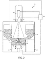
- Figure 2 depicts an embodiment of a freeform fabrication or additive manufacturing apparatus 21 in which the inventive method according to the present invention may be implemented.
- the apparatus 21 comprising an electron beam gun 6; deflection coils 7; two powder hoppers 4, 14; a build platform 2; a build tank 10; a powder distributor 28; a powder bed 5; and a vacuum chamber 20.
- the vacuum chamber 20 is capable of maintaining a vacuum environment via a vacuum system, which system may comprise a turbo molecular pump, a scroll pump, an ion pump and one or more valves which are well known to a skilled person in the art and therefore need no further explanation in this context.
- the vacuum system is controlled by a control unit 8.
- the electron beam gun 6 is generating an electron beam which is used for pre heating of the powder, melting or fusing together powder material provided on the build platform 2 or post heat treatment of the already fused powder material.
- the control unit 8 may be used for controlling and managing the electron beam emitted from the electron beam gun 6.
- At least one focusing coil (not shown), at least one deflection coil 7, an optional coil for astigmatic correction (not shown) and an electron beam power supply (not shown) may be electrically connected to the control unit 8.
- the electron beam gun 6 may generate a focusable electron beam with an accelerating voltage of about 15-60kV and with a beam power in the range of 3-10kW.
- the pressure in the vacuum chamber may be 3x10 -3 mbar or lower when building the three-dimensional article by fusing the powder layer by layer with the energy beam.
- the powder hoppers 4, 14 comprise the powder material to be provided on the build platform 2 in the build tank 10.
- the powder material may for instance be pure metals or metal alloys such as titanium, titanium alloys, aluminum, aluminum alloys, stainless steel, Co-Cr alloys, nickelbased super alloys, and the like.
- the powder distributor 28 is arranged to lay down a thin layer of the powder material on the build platform 2.
- the build platform 2 will be lowered successively in relation to a fixed point in the vacuum chamber.
- the build platform 2 is in one embodiment of the invention arranged movably in vertical direction, i.e., in the direction indicated by arrow P. This means that the build platform 2 starts in an initial position, in which a first powder material layer of necessary thickness has been laid down.
- Means for lowering the build platform 2 may for instance be through a servo motor equipped with a gear, adjusting screws, or the like.
- the servo motor may be connected to the control unit 8.
- An electron beam may be directed over the build platform 2 causing the first powder layer to fuse in selected locations to form a first cross section of the three-dimensional article 3.
- the beam is directed over the build platform 2 from instructions given by the control unit 8.
- instructions for how to control the electron beam for each layer of the three-dimensional article is stored.
- the first layer of the three dimensional article 3 may be built on the build platform 2, which may be removable, in the powder bed 5 or on an optional start plate 16.
- the start plate 16 may be arranged directly on the build platform 2 or on top of a powder bed 5 which is provided on the build platform 2.
- a second powder layer is provided on the build platform 2.
- the thickness of the second layer may be determined by the distance the build platform is lowered in relation to the position where the first layer was built.
- the second powder layer is in various embodiments distributed according to the same manner as the previous layer.
- a first layer may be provided via a first powder distributor 28, a second layer may be provided by another powder distributor.
- the design of the powder distributor is automatically changed according to instructions from the control unit 8.
- a powder distributor 28 in the form of a single rake system, i.e., where one rake is catching powder fallen down from both a left powder hopper 4 and a right powder hopper 14, the rake as such can change design.
- the energy beam is directed over the work table causing the second powder layer to fuse in selected locations to form a second cross section of the three-dimensional article.
- Fused portions in the second layer may be bonded to fused portions of the first layer.
- the fused portions in the first and second layer may be melted together by melting not only the powder in the uppermost layer but also remelting at least a fraction of a thickness of a layer directly below the uppermost layer.
- the charge distribution density depends on the following parameters: beam current, electron velocity (which is given by the accelerating voltage), beam scanning velocity, powder material and electrical conductivity of the powder, i.e., mainly the electrical conductivity between the powder grains.
- beam current electron velocity (which is given by the accelerating voltage)
- electron scanning velocity powder material
- electrical conductivity of the powder i.e., mainly the electrical conductivity between the powder grains.
- the latter is in turn a function of several parameters, such as the non-limiting examples of temperature, degree of sintering and powder grain size/size distribution.
- the electrical conductivity of the powder can gradually be increased by increasing the temperature of the powder.
- a powder that has a high temperature obtains a considerably higher conductivity which results in a lower density of the charge distribution since the charges quickly can diffuse over a large region. This effect is enhanced if the powder is allowed to be slightly sintered during a pre-heating process.
- the powder can be fused together, i.e., melted or fully sintered, with predetermined values of the beam current and beam scanning velocity.
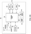
- FIG. 1 depicts, in a schematic cross sectional side view, an example embodiment of an electron beam source 100 according to the present invention.
- the electron beam source 100 comprises a cathode 101, a grid cup or Wehnelt cup 102 and an anode 104. Electrons 106 emitted at the cathode, 101 being on negative potential, are accelerated towards the anode 104 and finally a target surface (not shown).
- the grid cup 102 is set at a predetermined distance from the cathode 101.
- the cathode 101 may be provided with a separate power supply which may be used to heat the cathode, where upon the cathode 101 releases electrons by thermionic emission.
- An acceleration voltage 160 is provided between the cathode 101 and the anode 104.
- the acceleration voltage 160 causes the emitted electrons from the cathode 101 to accelerate towards the anode 104 thus establishing an electron beam 106.
- the electron beam 106 may impinge on a substrate surface, which may be a powder layer in an additive manufacturing process.
- a substrate surface which may be a powder layer in an additive manufacturing process.
- there may further be arranged at least one focusing coil and at least one deflection coil.
- the grid cup 102 is provided between the cathode 101 and the anode 104.
- the grid cup 102 may be arranged as a plate having an aperture 112.
- the aperture 112 may be aligned with the cathode 101.
- the size of the aperture 112 in the grid cup 102 may correspond to a cross section of the electron beam 106 at the position of the grid cup 102.
- a grid cup voltage 180 may be provided between the grid cup 102 and the cathode 101 and may be adjusted between a negative blocking voltage and a full power voltage and thereby adjusting an electron beam current between 0 - maximum electron beam current.
- the cathode 101 may be provided with a negative potential of -20kV to -100kV.
- the grid cup voltage 180 may be varied between the negative blocking voltage and the full power voltage.
- a grid amplifier 124 may be controlling the grid cup voltage 180 in order to adjust the electron beam current to a desired value as well as the acceleration voltage 160.
- the anode may be set to ground potential.
- the target surface may be set to ground potential or a positive potential.
- the electron beam source 100 may also comprise means for detecting the actual electron beam current.
- An example means for detecting the electron beam current on the target surface may be to detect the actual loading of the high voltage source providing the acceleration voltage 160. If the cathode is provided with a fixed negative potential of -60kV the negative blocking voltage may be around -61kV, i.e., the Wehnelt cup 102 itself is set at -61kV, for blocking the electrons by the grid cup 102. If starting to decrease the negative blocking potential, some of the electrons emitted from the cathode will be allowed to pass through the grid cup 102.
- the electron beam current may vary from 0mA - maximum electron beam current which may be 25mA for a predetermined size and shape of the cathode 101 and a predetermined size and shape of the aperture in the grid cup 102.
- Other acceleration voltages and/or other size, shape and emissivity of the cathode 101 and/or other size and shape of the aperture in the grid cup 102 may affect the maximum electron beam current to be higher or lower than the exemplified 25mA.
- the grid potential is in the example embodiment above referenced to the ground potential, however the grid potential may in another example embodiment be referenced to the cathode potential.
- the grid cup 102 may be provided with a clamping potential 170 under special circumstances in order to diverge vacuum discharge arcs from the cathode 101 towards and onto the grid cup 102.
- a pre-discharge channel 107 may be present between the anode 104 and the cathode 101 if no special measures are taken.
- a diverted discharge channel 108 between the anode 104 and the grid cup 102 may be present if the grid cup 102 is arranged with the clamping voltage which will have a more negative electric potential than the cathode 101 and the blocking voltage on the Wehnelt cup 102.
- a clamping voltage 170 may be fixed and connected to a bulk capacitance 105 of sufficient size to maintain its relative voltage to the cathode 101 during any possible vacuum discharge.
- the clamping potential 170 is what controls the electric field strength that attracts and diverges the developing pre-discharge arc channel 107 from the anode 104 to the cathode 101 into a diverted discharge channel 108 from the anode 104 to the grid cup 102.
- the clamping potential 170 may be provided onto the grid cup under the special circumstances, which in an example embodiment may be when a leakage current detector 120, 122 detects a leakage current which is above a predetermined value.
- a first leakage current detector 120 may detect a leakage current at the anode 104.
- a second leakage current detector 122 may detect a leakage current at the grid cup 102.
- the leakage current through the anode and/or the grid cup may be a first sign in a build-up phase of a vacuum arc discharge event. This leakage current may be used as a trigger signal to a switch. If the leakage current is above a predetermined value a control unit 150 may send a control signal to the switch 130, which in turn will close the switch 130.
- a closure of the switch 130 means that the clamping potential is applied to the grid cup 102 and the vacuum arc discharge is redirected from the cathode to the grid cup.
- the second control unit 150 may be a physically separate control unit or integrated with control unit 8 in Figure 2 .
- the leakage current detector may sense current anomalies in the range of ⁇ A to mA with a characteristic current derivative typical for a vacuum arc discharge build up.
- the time window for sensing the vacuum arc build up is narrow, typically in the range of 100ns to a few ⁇ s, and the switch 130 needs to be fully activated within this time window.
- the switch 130 may typically be realized by specialized power electronic devices such as triode electron tubes or high voltage power transistors.
- the detectors 120, 122 and clamping switch 130 may be realized as one unit possibly integrated with the cathode 101 and Wehnelt assembly 102.
- the clamping potential 170 needs to be around -61.5kV or higher if set to a fixed value.
- the clamping voltage potential is very much dependent of the geometries of the Wehnelt cup 102, cathode 101 and anode 104 as well as the acceleration voltage 160.
- the clamping potential may be at least - 500V below the zero current threshold voltage on the Wehnelt cup 102.
- the cathode element may be made of a rare earth metal oxide such as lanthanum hexaboride. In another example embodiment the cathode element may be made of a wolfram element.
- the cathode element may be heated by a separate heating circuit (not shown) in order to set the cathode element 101 to a desired temperature at which electron emission is favourable.
- the clamping voltage source may need to have a low impedance and sufficient current handling capacity to withstand the vacuum arc discharge current without dropping more than negligible in clamping voltage in order to sustain a sufficient potential difference with reference to the cathode 101 to maintain the diverging electric field strength at the Wehnelt cup 102.
- the capacitor 105 may be of a size in the range of a few ⁇ F up to 100 ⁇ F, where the size is dependent of the discharge energy and maximum allowed voltage drop during any foreseeable discharge.
- the clamping voltage source may be a low impedance negative voltage source.
- the clamping voltage source comprises a capacitor of sufficient size so as to maintain a more negative potential to the grid cup compared to the cathode during a time the vacuum discharge event take place.
- the clamping voltage may be in the order of -500 to -2000V lower than the Wehnelt cup cut off voltage.
- the clamping voltage has at least 1% more negative potential than the cathode element. In another example embodiment the clamping voltage has at least 2.5% more negative potential than the cathode element. In still another example embodiment the clamping potential is at least 1000V more negative than the cathode potential.
- Figure 3 depicts a schematic flow chart of an example embodiment of the method for forming a three-dimensional article through successively depositing individual layers of powder material that are fused together so as to form the article.
- a first step 310 at least one electron beam source is provided for emitting an electron beam for at least one of heating or fusing the powder material, wherein the electron beam source comprises a cathode, an anode, and a Wehnelt cup positioned between the cathode and anode.
- a leakage current detector is provided for sensing a current through the anode and/or the Wehnelt cup.
- a low impedance voltage source is provided and connectable to the Wehnelt cup via a switch, where the voltage source is having a more negative potential than a negative potential applied to the cathode.
- a fourth step 340 the cathode is protected against vacuum arc discharge energy currents when forming the three-dimensional article by providing the Wehnelt cup to the low impedance negative voltage by closing the switch when the leakage current detector is sensing a current through the anode and/or the Wehnelt cup which is higher than a predetermined value.
- a program element configured and arranged when executed on a computer to implement a method for forming a three-dimensional article through successively depositing individual layers of powder material that are fused together so as to form the article, the method comprising the steps of: providing at least one electron beam source emitting an electron beam for at least one of heating or fusing the powder material, wherein the electron beam source comprises a cathode, an anode, and a Wehnelt cup positioned between the cathode and anode; providing a leakage current detector for sensing a current through the anode and/or the Wehnelt cup; providing a low impedance voltage source connectable to the Wehnelt cup via a switch, where the voltage source is having a more negative potential than a negative potential applied to the cathode; and protecting the cathode against vacuum arc discharge energy currents when forming the three-dimensional article by providing the Wehnelt cup to the low impedance negative voltage source by closing the
- the program may be installed in a computer readable storage medium.
- the computer readable storage medium may be the control unit 8, the control unit 150, or another separate and distinct control unit.
- the computer readable storage medium and the program element, which may comprise computer-readable program code portions embodied therein, may further be contained within a non-transitory computer program product. Further details regarding these features and configurations are provided, in turn, below.
- a computer program product may include a non-transitory computer-readable storage medium storing applications, programs, program modules, scripts, source code, program code, object code, byte code, compiled code, interpreted code, machine code, executable instructions, and/or the like (also referred to herein as executable instructions, instructions for execution, program code, and/or similar terms used herein interchangeably).
- Such non-transitory computer-readable storage media include all computer-readable media (including volatile and non-volatile media).
- a non-volatile computer-readable storage medium may include a floppy disk, flexible disk, hard disk, solid-state storage (SSS) (e.g., a solid state drive (SSD), solid state card (SSC), solid state module (SSM)), enterprise flash drive, magnetic tape, or any other non-transitory magnetic medium, and/or the like.
- SSD solid state drive
- SSC solid state card
- SSM solid state module
- a non-volatile computer-readable storage medium may also include a punch card, paper tape, optical mark sheet (or any other physical medium with patterns of holes or other optically recognizable indicia), compact disc read only memory (CD-ROM), compact disc compact disc-rewritable (CD-RW), digital versatile disc (DVD), Blu-ray disc (BD), any other non-transitory optical medium, and/or the like.
- CD-ROM compact disc read only memory
- CD-RW compact disc compact disc-rewritable
- DVD digital versatile disc
- BD Blu-ray disc
- Such a nonvolatile computer-readable storage medium may also include read-only memory (ROM), programmable read-only memory (PROM), erasable programmable read-only memory (EPROM), electrically erasable programmable read-only memory (EEPROM), flash memory (e.g., Serial, NAND, NOR, and/or the like), multimedia memory cards (MMC), secure digital (SD) memory cards, SmartMedia cards, CompactFlash (CF) cards, Memory Sticks, and/or the like.
- ROM read-only memory
- PROM programmable read-only memory
- EPROM erasable programmable read-only memory
- EEPROM electrically erasable programmable read-only memory
- flash memory e.g., Serial, NAND, NOR, and/or the like
- MMC multimedia memory cards
- SD secure digital
- a non-volatile computer-readable storage medium may also include conductive-bridging random access memory (CBRAM), phase-change random access memory (PRAM), ferroelectric random-access memory (FeRAM), non-volatile random-access memory (NVRAM), magnetoresistive random-access memory (MRAM), resistive random-access memory (RRAM), Silicon-Oxide-Nitride-Oxide-Silicon memory (SONOS), floating junction gate random access memory (FJG RAM), Millipede memory, racetrack memory, and/or the like.
- CBRAM conductive-bridging random access memory
- PRAM phase-change random access memory
- FeRAM ferroelectric random-access memory
- NVRAM non-volatile random-access memory
- MRAM magnetoresistive random-access memory
- RRAM resistive random-access memory
- SONOS Silicon-Oxide-Nitride-Oxide-Silicon memory
- FJG RAM floating junction gate random access memory
- Millipede memory racetrack memory
- a volatile computer-readable storage medium may include random access memory (RAM), dynamic random access memory (DRAM), static random access memory (SRAM), fast page mode dynamic random access memory (FPM DRAM), extended dataout dynamic random access memory (EDO DRAM), synchronous dynamic random access memory (SDRAM), double data rate synchronous dynamic random access memory (DDR SDRAM), double data rate type two synchronous dynamic random access memory (DDR2 SDRAM), double data rate type three synchronous dynamic random access memory (DDR3 SDRAM), Rambus dynamic random access memory (RDRAM), Twin Transistor RAM (TTRAM), Thyristor RAM (T-RAM), Zero-capacitor (Z-RAM), Rambus in-line memory module (RIMM), dual in-line memory module (DIMM), single in-line memory module (SIMM), video random access memory VRAM, cache memory (including various levels), flash memory, register memory, and/or the like.
- RAM random access memory
- DRAM dynamic random access memory
- SRAM static random access memory
- FPM DRAM fast page mode dynamic random access memory
- embodiments of the present invention may also be implemented as methods, apparatus, systems, computing devices, computing entities, and/or the like, as have been described elsewhere herein.
- embodiments of the present invention may take the form of an apparatus, system, computing device, computing entity, and/or the like executing instructions stored on a computer-readable storage medium to perform certain steps or operations.
- embodiments of the present invention may also take the form of an entirely hardware embodiment performing certain steps or operations.
- These computer program instructions may also be stored in a computer-readable memory that can direct a computer or other programmable data processing apparatus to function in a particular manner, such that the instructions stored in the computer-readable memory produce an article of manufacture including computer-readable instructions for implementing the functionality specified in the flowchart block or blocks.
- the computer program instructions may also be loaded onto a computer or other programmable data processing apparatus to cause a series of operational steps to be performed on the computer or other programmable apparatus to produce a computer-implemented process such that the instructions that execute on the computer or other programmable apparatus provide operations for implementing the functions specified in the flowchart block or blocks.
- blocks of the block diagrams and flowchart illustrations support various combinations for performing the specified functions, combinations of operations for performing the specified functions and program instructions for performing the specified functions. It should also be understood that each block of the block diagrams and flowchart illustrations, and combinations of blocks in the block diagrams and flowchart illustrations, could be implemented by special purpose hardware-based computer systems that perform the specified functions or operations, or combinations of special purpose hardware and computer instructions.
- Figure 4 is a block diagram of an exemplary system 1020 that can be used in conjunction with various embodiments of the present invention.
- the system 1020 may include one or more central computing devices 1110, one or more distributed computing devices 1120, and one or more distributed handheld or mobile devices 1300, all configured in communication with a central server 1200 (or control unit) via one or more networks 1130.
- Figure 4 illustrates the various system entities as separate, standalone entities, the various embodiments are not limited to this particular architecture.
- the one or more networks 1130 may be capable of supporting communication in accordance with any one or more of a number of second-generation (2G), 2.5G, third-generation (3G), and/or fourth-generation (4G) mobile communication protocols, or the like. More particularly, the one or more networks 1130 may be capable of supporting communication in accordance with 2G wireless communication protocols IS-136 (TDMA), GSM, and IS-95 (CDMA). Also, for example, the one or more networks 1130 may be capable of supporting communication in accordance with 2.5G wireless communication protocols GPRS, Enhanced Data GSM Environment (EDGE), or the like.
- the one or more networks 1130 may be capable of supporting communication in accordance with 3G wireless communication protocols such as Universal Mobile Telephone System (UMTS) network employing Wideband Code Division Multiple Access (WCDMA) radio access technology.
- UMTS Universal Mobile Telephone System
- WCDMA Wideband Code Division Multiple Access
- Some narrow-band AMPS (NAMPS), as well as TACS, network(s) may also benefit from embodiments of the present invention, as should dual or higher mode mobile stations (e.g., digital/analog or TDMA/CDMA/analog phones).
- each of the components of the system 1020 may be configured to communicate with one another in accordance with techniques such as, for example, radio frequency (RF), BluetoothTM, infrared (IrDA), or any of a number of different wired or wireless networking techniques, including a wired or wireless Personal Area Network (“PAN”), Local Area Network (“LAN”), Metropolitan Area Network (“MAN”), Wide Area Network (“WAN”), or the like.
- RF radio frequency
- IrDA infrared
- PAN Personal Area Network
- LAN Local Area Network
- MAN Metropolitan Area Network
- WAN Wide Area Network
- the device(s) 1110-1300 are illustrated in Figure 4 as communicating with one another over the same network 1130, these devices may likewise communicate over multiple, separate networks.
- the distributed devices 1110, 1120, and/or 1300 may be further configured to collect and transmit data on their own.
- the devices 1110, 1120, and/or 1300 may be capable of receiving data via one or more input units or devices, such as a keypad, touchpad, barcode scanner, radio frequency identification (RFID) reader, interface card (e.g., modem, etc.) or receiver.
- RFID radio frequency identification
- the devices 1110, 1120, and/or 1300 may further be capable of storing data to one or more volatile or non-volatile memory modules, and outputting the data via one or more output units or devices, for example, by displaying data to the user operating the device, or by transmitting data, for example over the one or more networks 1130.
- the server 1200 includes various systems for performing one or more functions in accordance with various embodiments of the present invention, including those more particularly shown and described herein. It should be understood, however, that the server 1200 might include a variety of alternative devices for performing one or more like functions, without departing from the spirit and scope of the present invention. For example, at least a portion of the server 1200, in certain embodiments, may be located on the distributed device(s) 1110, 1120, and/or the handheld or mobile device(s) 1300, as may be desirable for particular applications.
- the handheld or mobile device(s) 1300 may contain one or more mobile applications 1330 which may be configured so as to provide a user interface for communication with the server 1200, all as will be likewise described in further detail below.
- FIG. 5A is a schematic diagram of the server 1200 according to various embodiments.
- the server 1200 includes a processor 1230 that communicates with other elements within the server via a system interface or bus 1235. Also included in the server 1200 is a display/input device 1250 for receiving and displaying data. This display/input device 1250 may be, for example, a keyboard or pointing device that is used in combination with a monitor.
- the server 1200 further includes memory 1220, which preferably includes both read only memory (ROM) 1226 and random access memory (RAM) 1222.
- the server's ROM 1226 is used to store a basic input/output system 1224 (BIOS), containing the basic routines that help to transfer information between elements within the server 1200.
- BIOS basic input/output system
- the server 1200 includes at least one storage device or program storage 210, such as a hard disk drive, a floppy disk drive, a CD Rom drive, or optical disk drive, for storing information on various computer-readable media, such as a hard disk, a removable magnetic disk, or a CD-ROM disk.
- each of these storage devices 1210 are connected to the system bus 1235 by an appropriate interface.
- the storage devices 1210 and their associated computer-readable media provide nonvolatile storage for a personal computer.
- the computer-readable media described above could be replaced by any other type of computer-readable media known in the art. Such media include, for example, magnetic cassettes, flash memory cards, digital video disks, and Bernoulli cartridges.
- the storage device 1210 and/or memory of the server 1200 may further provide the functions of a data storage device, which may store historical and/or current delivery data and delivery conditions that may be accessed by the server.
- the storage device 1210 may comprise one or more databases.
- database refers to a structured collection of records or data that is stored in a computer system, such as via a relational database, hierarchical database, or network database and as such, should not be construed in a limiting fashion.
- a number of program modules comprising, for example, one or more computer-readable program code portions executable by the processor 1230, may be stored by the various storage devices 1210 and within RAM 1222. Such program modules may also include an operating system 1280.
- the various modules 1400, 1500, 1600, 1700 control certain aspects of the operation of the server 1200 with the assistance of the processor 1230 and operating system 1280.
- one or more additional and/or alternative modules may also be provided, without departing from the scope and nature of the present invention.
- the program modules 1400, 1500, 1600, 1700 are executed by the server 1200 and are configured to generate one or more graphical user interfaces, reports, instructions, and/or notifications/alerts, all accessible and/or transmittable to various users of the system 1020.
- the user interfaces, reports, instructions, and/or notifications/alerts may be accessible via one or more networks 1130, which may include the Internet or other feasible communications network, as previously discussed.
- one or more of the modules 1400, 1500, 1600, 1700 may be alternatively and/or additionally (e.g., in duplicate) stored locally on one or more of the devices 1110, 1120, and/or 1300 and may be executed by one or more processors of the same.
- the modules 1400, 1500, 1600, 1700 may send data to, receive data from, and utilize data contained in one or more databases, which may be comprised of one or more separate, linked and/or networked databases.
- a network interface 1260 for interfacing and communicating with other elements of the one or more networks 1130. It will be appreciated by one of ordinary skill in the art that one or more of the server 1200 components may be located geographically remotely from other server components. Furthermore, one or more of the server 1060 components may be combined, and/or additional components performing functions described herein may also be included in the server.
- the server 1200 may comprise multiple processors operating in conjunction with one another to perform the functionality described herein.
- the processor 1230 can also be connected to at least one interface or other means for displaying, transmitting and/or receiving data, content or the like.
- the interface(s) can include at least one communication interface or other means for transmitting and/or receiving data, content or the like, as well as at least one user interface that can include a display and/or a user input interface, as will be described in further detail below.
- the user input interface in turn, can comprise any of a number of devices allowing the entity to receive data from a user, such as a keypad, a touch display, a joystick or other input device.
- embodiments of the present invention are not limited to traditionally defined server architectures. Still further, the system of embodiments of the present invention is not limited to a single server, or similar network entity or mainframe computer system. Other similar architectures including one or more network entities operating in conjunction with one another to provide the functionality described herein may likewise be used without departing from the spirit and scope of embodiments of the present invention. For example, a mesh network of two or more personal computers (PCs), similar electronic devices, or handheld portable devices, collaborating with one another to provide the functionality described herein in association with the server 1200 may likewise be used without departing from the spirit and scope of embodiments of the present invention.
- PCs personal computers
- similar electronic devices or handheld portable devices
- many individual steps of a process may or may not be carried out utilizing the computer systems and/or servers described herein, and the degree of computer implementation may vary, as may be desirable and/or beneficial for one or more particular applications.
- FIG. 5B provides an illustrative schematic representative of a mobile device 1300 that can be used in conjunction with various embodiments of the present invention.
- Mobile devices 1300 can be operated by various parties.
- a mobile device 1300 may include an antenna 1312, a transmitter 1304 (e.g., radio), a receiver 1306 (e.g., radio), and a processing element 1308 that provides signals to and receives signals from the transmitter 1304 and receiver 1306, respectively.
- a transmitter 1304 e.g., radio
- a receiver 1306 e.g., radio
- a processing element 1308 that provides signals to and receives signals from the transmitter 1304 and receiver 1306, respectively.
- the signals provided to and received from the transmitter 1304 and the receiver 1306, respectively, may include signaling data in accordance with an air interface standard of applicable wireless systems to communicate with various entities, such as the server 1200, the distributed devices 1110, 1120, and/or the like.
- the mobile device 1300 may be capable of operating with one or more air interface standards, communication protocols, modulation types, and access types. More particularly, the mobile device 1300 may operate in accordance with any of a number of wireless communication standards and protocols.
- the mobile device 1300 may operate in accordance with multiple wireless communication standards and protocols, such as GPRS, UMTS, CDMA2000, 1xRTT, WCDMA, TD-SCDMA, LTE, E-UTRAN, EVDO, HSPA, HSDPA, Wi-Fi, WiMAX, UWB, IR protocols, Bluetooth protocols, USB protocols, and/or any other wireless protocol.
- multiple wireless communication standards and protocols such as GPRS, UMTS, CDMA2000, 1xRTT, WCDMA, TD-SCDMA, LTE, E-UTRAN, EVDO, HSPA, HSDPA, Wi-Fi, WiMAX, UWB, IR protocols, Bluetooth protocols, USB protocols, and/or any other wireless protocol.
- the mobile device 1300 may according to various embodiments communicate with various other entities using concepts such as Unstructured Supplementary Service data (USSD), Short Message Service (SMS), Multimedia Messaging Service (MMS), Dual-Tone Multi-Frequency Signaling (DTMF), and/or Subscriber Identity Module Dialer (SIM dialer).
- USSD Unstructured Supplementary Service data
- SMS Short Message Service
- MMS Multimedia Messaging Service
- DTMF Dual-Tone Multi-Frequency Signaling
- SIM dialer Subscriber Identity Module Dialer
- the mobile device 1300 can also download changes, addons, and updates, for instance, to its firmware, software (e.g., including executable instructions, applications, program modules), and operating system.
- the mobile device 1300 may include a location determining device and/or functionality.
- the mobile device 1300 may include a GPS module adapted to acquire, for example, latitude, longitude, altitude, geocode, course, and/or speed data.
- the GPS module acquires data, sometimes known as ephemeris data, by identifying the number of satellites in view and the relative positions of those satellites.
- the mobile device 1300 may also comprise a user interface (that can include a display 1316 coupled to a processing element 1308) and/or a user input interface (coupled to a processing element 1308).
- the user input interface can comprise any of a number of devices allowing the mobile device 1300 to receive data, such as a keypad 1318 (hard or soft), a touch display, voice or motion interfaces, or other input device.
- the keypad can include (or cause display of) the conventional numeric (0-9) and related keys (#, *), and other keys used for operating the mobile device 1300 and may include a full set of alphabetic keys or set of keys that may be activated to provide a full set of alphanumeric keys.
- the user input interface can be used, for example, to activate or deactivate certain functions, such as screen savers and/or sleep modes.
- the mobile device 1300 can also include volatile storage or memory 1322 and/or nonvolatile storage or memory 1324, which can be embedded and/or may be removable.
- the non-volatile memory may be ROM, PROM, EPROM, EEPROM, flash memory, MMCs, SD memory cards, Memory Sticks, CBRAM, PRAM, FeRAM, RRAM, SONOS, racetrack memory, and/or the like.
- the volatile memory may be RAM, DRAM, SRAM, FPM DRAM, EDO DRAM, SDRAM, DDR SDRAM, DDR2 SDRAM, DDR3 SDRAM, RDRAM, RIMM, DIMM, SIMM, VRAM, cache memory, register memory, and/or the like.
- the volatile and non-volatile storage or memory can store databases, database instances, database mapping systems, data, applications, programs, program modules, scripts, source code, object code, byte code, compiled code, interpreted code, machine code, executable instructions, and/or the like to implement the functions of the mobile device 1300.
- the mobile device 1300 may also include one or more of a camera 1326 and a mobile application 1330.
- the camera 1326 may be configured according to various embodiments as an additional and/or alternative data collection feature, whereby one or more items may be read, stored, and/or transmitted by the mobile device 1300 via the camera.
- the mobile application 1330 may further provide a feature via which various tasks may be performed with the mobile device 1300.
- Various configurations may be provided, as may be desirable for one or more users of the mobile device 1300 and the system 1020 as a whole.
Landscapes
- Engineering & Computer Science (AREA)
- Chemical & Material Sciences (AREA)
- Materials Engineering (AREA)
- Manufacturing & Machinery (AREA)
- Physics & Mathematics (AREA)
- Mechanical Engineering (AREA)
- Optics & Photonics (AREA)
- Analytical Chemistry (AREA)
- Plasma & Fusion (AREA)
- Toxicology (AREA)
- Health & Medical Sciences (AREA)
- Automation & Control Theory (AREA)
- Ceramic Engineering (AREA)
- Composite Materials (AREA)
- General Health & Medical Sciences (AREA)
- Powder Metallurgy (AREA)
Claims (15)
- Verfahren zur Herstellung eines dreidimensionalen Werkstücks durch aufeinanderfolgendes Auftragen von einzelnen Schichten aus Pulvermaterial, die miteinander verschmolzen werden, um das Werkstück herzustellen, wobei das Verfahren die folgenden Schritte umfasst:Emittieren eines Elektronenstrahls (106) mittels mindestens einer Elektronenstrahlquelle (100) zum Erhitzen oder Verschmelzen des Pulvermaterials, worin die Elektronenstrahlquelle (100) eine Kathode (101), eine Anode (104) und einen zwischen der Kathode (101) und der Anode (104) angeordneten Wehnelt-Zylinder (102) umfasst;Anlegen eines negativen Potentials an die Kathode (101);gekennzeichnet durchErfassen eines Stroms durch die Anode (104) und/oder den Wehnelt-Zylinder (102) über einen Leckstromdetektor (120, 122); undals Reaktion darauf, dass der Strom durch die Anode (104) und/oder den Wehnelt-Zylinder (102) einen festgelegten Wert überschreitet, wird ein Umschalter (130) geschlossen, um den Wehnelt-Zylinder (102) mit einer Spannungsquelle (170) niedriger Impedanz zu verbinden, wobei die Spannungsquelle (170) ein negatives Potential aufweist, das negativer ist als das negative Potential, das an die Kathode (101) angelegt wird, wobei das Schließen des Umschalters die Kathode (101) vor Vakuum-Entladungsenergieströmen schützt, während das dreidimensionale Werkstück hergestellt wird.
- Verfahren nach Anspruch 1, worin die Kathode (101) aus einem Seltenerdmetalloxidmaterial besteht.
- Verfahren nach Anspruch 1, worin die niederohmige negative Spannungsquelle (170) einen Kondensator (105) mit einer Kapazität umfasst, die so konfiguriert ist, dass sie das negativere Potential an dem Wehnelt-Zylinder (102) im Vergleich zu dem an die Kathode (101) angelegten negativen Potential für den Zeitraum einer Vakuumentladung aufrechterhält.
- Verfahren nach Anspruch 3, worin die niederohmige negative Spannungsquelle (170) eine negative Spannung bereitstellt, die um mindestens 1000 V negativer ist als eine an der Kathode (101) bereitgestellte negative Spannung, wenn der Leckstromdetektor (120, 122) einen Strom durch die Anode (104) und/oder den Wehnelt-Zylinder (102) erfasst, der höher als der festgelegte Wert ist.
- Verfahren nach Anspruch 1, worin einer oder mehrere der dort genannten Schritte über mindestens eine Steuereinheit (150) oder einen Prozessor computerimplementiert sind.
- Verfahren nach Anspruch 1, worin der Umschalter (130) automatisch über mindestens eine Steuereinheit (150) geschlossen wird, wenn ein Strom erfasst wird, der höher als der festgelegte Wert ist.
- Additive Herstellungsvorrichtung (21) zum Bilden eines dreidimensionalen Werkstücks durch aufeinanderfolgendes Verschmelzen von Teilen mindestens einer auf einem Arbeitstisch (2) vorgesehenen Pulverschicht (5), wobei die Teile aufeinanderfolgenden Querschnitten des dreidimensionalen Werkstücks entsprechen, wobei die Vorrichtung (21) umfasst:mindestens eine Elektronenstrahlquelle (100), die einen Elektronenstrahl (106) zum Erhitzen und/oder Schmelzen des Pulvermaterials (5) aussendet, worin die Elektronenstrahlquelle (100) eine Kathode (101), eine Anode (104) und einen Wehnelt-Zylinder (102) umfasst, der zwischen der Kathode (101) und der Anode (104) angeordnet ist;gekennzeichnet durcheinen Leckstromdetektor (120, 122), der zum Erfassen eines Leckstroms durch die Anode (104) und/oder den Wehnelt-Zylinder (102) konfiguriert ist;eine Spannungsquelle (170) mit niedriger Impedanz, die über einen Umschalter (130) selektiv mit dem Wehnelt-Zylinder (102) verbunden werden kann, wobei die Spannungsquelle (170) ein negativeres Potential aufweist als ein an die Kathode (101) angelegtes negatives Potential; undeine Steuervorrichtung (150),worin als Reaktion auf das Erfassen eines Stroms durch die Anode (104) und/oder den Wehnelt-Zylinder (102), der größer als ein festgelegter Wert ist, der Umschalter (130) über die Steuervorrichtung (150) geschlossen wird, um die Spannungsquelle (170) mit dem Wehnelt-Zylinder (102) zu verbinden.
- Vorrichtung gemäß Anspruch 7, worin die niederohmige negative Spannungsquelle (170) eine elektrische Schaltung ist, die dazu bestimmt ist, während der Vakuumentladung ein negatives Potential aufrechtzuerhalten, das negativer ist als das an die Kathode (101) angelegte negative Potential.
- Vorrichtung nach Anspruch 7, worin die Steuereinrichtung (150) zum Einstellen des Wehnelt-Zylinderpotentials auf ein negativeres Potential als das Kathodenpotential konfiguriert ist.
- Vorrichtung nach Anspruch 7, worin die Kathode (101) aus einem Seltenerdmetalloxidmaterial besteht.
- Vorrichtung nach Anspruch 7, worin die niederohmige negative Spannungsquelle (170) einen Kondensator (105) mit einer Kapazität umfasst, die so konfiguriert ist, dass sie ein negativeres Potential zum Gitter im Vergleich zur Kathode (101) für den Zeitraum einer Vakuumentladung aufrechterhält.
- Vorrichtung nach Anspruch 7, worin die niederohmige negative Spannungsquelle (170) eine negative Spannung bereitstellt, die um mindestens 1000 V negativer ist als eine an der Kathode (101) bereitgestellte negative Spannung, wenn der Leckstromdetektor (120, 122) einen Strom durch die Anode (104) und/oder den Wehnelt-Zylinder (102) erfasst, der höher als der festgelegte Wert ist.
- Computerprogrammprodukt, das mindestens ein nicht-transitorisches computerlesbares Speichermedium mit darin enthaltenen computerlesbaren Programmcodeanteilen umfasst, wobei die computerlesbaren Programmcodeanteile mindestens einen ausführbaren Anteil umfassen, der konfiguriert ist,
dass er die Vorrichtung nach Anspruch 7 anweist, das Verfahren nach einem der Ansprüche 1 bis 4 durchzuführen. - Computerprogrammprodukt nach Anspruch 13, worin der mindestens eine ausführbare Anteil so konfiguriert ist, dass er den Umschalter (130) automatisch schließt, wenn er den Strom erfasst, der höher als der festgelegte Wert ist.
- Computerprogrammprodukt nach Anspruch 13, worin der mindestens eine ausführbare Anteil ferner zum Einstellen des Wehnelt-Zylinderpotentials auf ein negativeres Potential als das Kathodenpotential konfiguriert ist.
Applications Claiming Priority (3)
| Application Number | Priority Date | Filing Date | Title |
|---|---|---|---|
| US201662437119P | 2016-12-21 | 2016-12-21 | |
| US15/790,348 US10987752B2 (en) | 2016-12-21 | 2017-10-23 | Additive manufacturing of three-dimensional articles |
| PCT/EP2017/079081 WO2018114142A1 (en) | 2016-12-21 | 2017-11-13 | Additive manufacturing of three-dimensional articles |
Publications (2)
| Publication Number | Publication Date |
|---|---|
| EP3559975A1 EP3559975A1 (de) | 2019-10-30 |
| EP3559975B1 true EP3559975B1 (de) | 2021-06-23 |
Family
ID=62556188
Family Applications (1)
| Application Number | Title | Priority Date | Filing Date |
|---|---|---|---|
| EP17808796.1A Active EP3559975B1 (de) | 2016-12-21 | 2017-11-13 | Generative fertigung von dreidimensionalen artikeln |
Country Status (5)
| Country | Link |
|---|---|
| US (1) | US10987752B2 (de) |
| EP (1) | EP3559975B1 (de) |
| JP (1) | JP6882485B2 (de) |
| CN (1) | CN110301026B (de) |
| WO (1) | WO2018114142A1 (de) |
Families Citing this family (5)
| Publication number | Priority date | Publication date | Assignee | Title |
|---|---|---|---|---|
| JP7007151B2 (ja) * | 2017-10-19 | 2022-01-24 | 株式会社アドバンテスト | 三次元積層造形装置および積層造形方法 |
| US11167375B2 (en) | 2018-08-10 | 2021-11-09 | The Research Foundation For The State University Of New York | Additive manufacturing processes and additively manufactured products |
| US10573481B1 (en) * | 2018-11-28 | 2020-02-25 | Nuflare Technology, Inc. | Electron guns for electron beam tools |
| CN111250854B (zh) * | 2020-02-10 | 2021-07-20 | 哈尔滨工业大学 | 用于电子束熔丝增材制造的局部冷却辅助装置及方法 |
| CN114834038B (zh) * | 2021-02-02 | 2024-08-02 | 湖州超群电子科技有限公司 | 一种电子束3d打印系统及其使用方法 |
Family Cites Families (239)
| Publication number | Priority date | Publication date | Assignee | Title |
|---|---|---|---|---|
| US2264968A (en) | 1938-02-14 | 1941-12-02 | Magnafiux Corp | Apparatus for measuring wall thickness |
| US2323715A (en) | 1941-10-17 | 1943-07-06 | Gen Electric | Thermal testing apparatus |
| US3064165A (en) * | 1960-05-23 | 1962-11-13 | Collins Radio Co | Relay speed-up circuit |
| US3634644A (en) | 1968-12-30 | 1972-01-11 | Ogden Eng Corp | Method and apparatus for welding together beam components |
| US3882477A (en) | 1973-03-26 | 1975-05-06 | Peter H Mueller | Smoke and heat detector incorporating an improved smoke chamber |
| US3838496A (en) | 1973-04-09 | 1974-10-01 | C Kelly | Welding apparatus and method |
| US3906229A (en) | 1973-06-12 | 1975-09-16 | Raytheon Co | High energy spatially coded image detecting systems |
| US3908124A (en) | 1974-07-01 | 1975-09-23 | Us Energy | Phase contrast in high resolution electron microscopy |
| US4348576A (en) | 1979-01-12 | 1982-09-07 | Steigerwald Strahltechnik Gmbh | Position regulation of a charge carrier beam |
| US4314134A (en) | 1979-11-23 | 1982-02-02 | Ford Motor Company | Beam position control for electron beam welder |
| JPS56156767A (en) | 1980-05-02 | 1981-12-03 | Sumitomo Electric Ind Ltd | Highly hard substance covering material |
| US4352565A (en) | 1981-01-12 | 1982-10-05 | Rowe James M | Speckle pattern interferometer |
| US4541055A (en) | 1982-09-01 | 1985-09-10 | Westinghouse Electric Corp. | Laser machining system |
| JPS59211950A (ja) | 1983-05-16 | 1984-11-30 | Mitsubishi Electric Corp | 電子ビ−ム加工装置 |
| JPS60181638A (ja) | 1984-02-29 | 1985-09-17 | Toshiba Corp | 放射線像撮影装置 |
| IL84936A (en) | 1987-12-23 | 1997-02-18 | Cubital Ltd | Three-dimensional modelling apparatus |
| US4863538A (en) | 1986-10-17 | 1989-09-05 | Board Of Regents, The University Of Texas System | Method and apparatus for producing parts by selective sintering |
| EP0289116A1 (de) | 1987-03-04 | 1988-11-02 | Westinghouse Electric Corporation | Verfahren und Vorrichtung zum Giessen von pulverförmigen Materialien |
| US4927992A (en) | 1987-03-04 | 1990-05-22 | Westinghouse Electric Corp. | Energy beam casting of metal articles |
| US4818562A (en) | 1987-03-04 | 1989-04-04 | Westinghouse Electric Corp. | Casting shapes |
| DE3736391C1 (de) | 1987-10-28 | 1989-02-16 | Du Pont Deutschland | Verfahren zum Beschichten von vorher klebrig gemachten Oberflaechenbereichen |
| US4958431A (en) | 1988-03-14 | 1990-09-25 | Westinghouse Electric Corp. | More creep resistant turbine rotor, and procedures for repair welding of low alloy ferrous turbine components |
| US4888490A (en) | 1988-05-24 | 1989-12-19 | University Of Southern California | Optical proximity apparatus and method using light sources being modulated at different frequencies |
| US5876550A (en) | 1988-10-05 | 1999-03-02 | Helisys, Inc. | Laminated object manufacturing apparatus and method |
| DE3923899A1 (de) | 1989-07-19 | 1991-01-31 | Leybold Ag | Verfahren fuer die regelung der auftreffpositionen von mehreren elektronenstrahlen auf ein schmelzbad |
| US5182170A (en) | 1989-09-05 | 1993-01-26 | Board Of Regents, The University Of Texas System | Method of producing parts by selective beam interaction of powder with gas phase reactant |
| US5135695A (en) | 1989-12-04 | 1992-08-04 | Board Of Regents The University Of Texas System | Positioning, focusing and monitoring of gas phase selective beam deposition |
| US5204055A (en) | 1989-12-08 | 1993-04-20 | Massachusetts Institute Of Technology | Three-dimensional printing techniques |
| US5118192A (en) | 1990-07-11 | 1992-06-02 | Robotic Vision Systems, Inc. | System for 3-D inspection of objects |
| JPH04332537A (ja) | 1991-05-03 | 1992-11-19 | Horiba Ltd | 骨塩測定方法 |
| US5252264A (en) | 1991-11-08 | 1993-10-12 | Dtm Corporation | Apparatus and method for producing parts with multi-directional powder delivery |
| JP3100209B2 (ja) | 1991-12-20 | 2000-10-16 | 三菱重工業株式会社 | 真空蒸着用偏向電子銃装置 |
| US5393482A (en) | 1993-10-20 | 1995-02-28 | United Technologies Corporation | Method for performing multiple beam laser sintering employing focussed and defocussed laser beams |
| US5483036A (en) | 1993-10-28 | 1996-01-09 | Sandia Corporation | Method of automatic measurement and focus of an electron beam and apparatus therefor |
| DE4400523C2 (de) | 1994-01-11 | 1996-07-11 | Eos Electro Optical Syst | Verfahren und Vorrichtung zum Herstellen eines dreidimensionalen Objekts |
| US5906863A (en) | 1994-08-08 | 1999-05-25 | Lombardi; John | Methods for the preparation of reinforced three-dimensional bodies |
| US5511103A (en) | 1994-10-19 | 1996-04-23 | Seiko Instruments Inc. | Method of X-ray mapping analysis |
| US5572431A (en) | 1994-10-19 | 1996-11-05 | Bpm Technology, Inc. | Apparatus and method for thermal normalization in three-dimensional article manufacturing |
| DE19511772C2 (de) | 1995-03-30 | 1997-09-04 | Eos Electro Optical Syst | Vorrichtung und Verfahren zum Herstellen eines dreidimensionalen Objektes |
| US5595670A (en) | 1995-04-17 | 1997-01-21 | The Twentyfirst Century Corporation | Method of high speed high power welding |
| US5837960A (en) | 1995-08-14 | 1998-11-17 | The Regents Of The University Of California | Laser production of articles from powders |
| DE19606128A1 (de) | 1996-02-20 | 1997-08-21 | Eos Electro Optical Syst | Vorrichtung und Verfahren zum Herstellen eines dreidimensionalen Objektes |
| US5883357A (en) | 1996-03-25 | 1999-03-16 | Case Western Reserve University | Selective vacuum gripper |
| US6046426A (en) | 1996-07-08 | 2000-04-04 | Sandia Corporation | Method and system for producing complex-shape objects |
| DE19846478C5 (de) | 1998-10-09 | 2004-10-14 | Eos Gmbh Electro Optical Systems | Laser-Sintermaschine |
| DE19853947C1 (de) | 1998-11-23 | 2000-02-24 | Fraunhofer Ges Forschung | Prozeßkammer für das selektive Laser-Schmelzen |
| US6162378A (en) | 1999-02-25 | 2000-12-19 | 3D Systems, Inc. | Method and apparatus for variably controlling the temperature in a selective deposition modeling environment |
| FR2790418B1 (fr) | 1999-03-01 | 2001-05-11 | Optoform Sarl Procedes De Prot | Procede de prototypage rapide permettant l'utilisation de materiaux pateux, et dispositif pour sa mise en oeuvre |
| US6204469B1 (en) | 1999-03-04 | 2001-03-20 | Honda Giken Kogyo Kabushiki Kaisha | Laser welding system |
| US6811744B2 (en) | 1999-07-07 | 2004-11-02 | Optomec Design Company | Forming structures from CAD solid models |
| US6391251B1 (en) | 1999-07-07 | 2002-05-21 | Optomec Design Company | Forming structures from CAD solid models |
| DE19939616C5 (de) | 1999-08-20 | 2008-05-21 | Eos Gmbh Electro Optical Systems | Vorrichtung zur generativen Herstellung eines dreidimensionalen Objektes |
| US6537052B1 (en) | 1999-08-23 | 2003-03-25 | Richard J. Adler | Method and apparatus for high speed electron beam rapid prototyping |
| US6362563B1 (en) * | 1999-10-05 | 2002-03-26 | Chunghwa Picture Tubes, Ltd. | Two-layer cathode for electron gun |
| DE19952998B4 (de) | 1999-11-04 | 2004-04-15 | Exner, Horst, Prof. Dr.-Ing. | Vorrichtung zur direkten Herstellung von Körpern im Schichtaufbau aus pulverförmigen Stoffen |
| SE521124C2 (sv) | 2000-04-27 | 2003-09-30 | Arcam Ab | Anordning samt metod för framställande av en tredimensionell produkt |
| AU2001275164A1 (en) | 2000-06-01 | 2001-12-11 | Board Of Regents, The University Of Texas System | Direct selective laser sintering of metals |
| SE520565C2 (sv) | 2000-06-16 | 2003-07-29 | Ivf Industriforskning Och Utve | Sätt och apparat vid framställning av föremål genom FFF |
| US20020020164A1 (en) | 2000-07-26 | 2002-02-21 | Cleveland Bradley A. | Tubular body with deposited features and method of manufacture therefor |
| US6751516B1 (en) | 2000-08-10 | 2004-06-15 | Richardson Technologies, Inc. | Method and system for direct writing, editing and transmitting a three dimensional part and imaging systems therefor |
| DE10047615A1 (de) | 2000-09-26 | 2002-04-25 | Generis Gmbh | Wechselbehälter |
| DE10058748C1 (de) | 2000-11-27 | 2002-07-25 | Markus Dirscherl | Verfahren zur Herstellung eines Bauteils sowie Vorrichtung zur Durchführung des Verfahrens |
| US6492651B2 (en) | 2001-02-08 | 2002-12-10 | 3D Systems, Inc. | Surface scanning system for selective deposition modeling |
| EP1234625A1 (de) | 2001-02-21 | 2002-08-28 | Trumpf Werkzeugmaschinen GmbH + Co. KG | Verfahren und Vorrichtung zur Herstellung eines Formkörpers durch selektives Laserschmelzen |
| US6732943B2 (en) | 2001-04-05 | 2004-05-11 | Aradigm Corporation | Method of generating uniform pores in thin polymer films |
| US6656410B2 (en) | 2001-06-22 | 2003-12-02 | 3D Systems, Inc. | Recoating system for using high viscosity build materials in solid freeform fabrication |
| US6419203B1 (en) | 2001-07-20 | 2002-07-16 | Chi Hung Dang | Vibration isolator with parallelogram mechanism |
| US7275925B2 (en) | 2001-08-30 | 2007-10-02 | Micron Technology, Inc. | Apparatus for stereolithographic processing of components and assemblies |
| DE10157647C5 (de) | 2001-11-26 | 2012-03-08 | Cl Schutzrechtsverwaltungs Gmbh | Verfahren zur Herstellung von dreidimensionalen Werkstücken in einer Laser-Materialbearbeitungsanlage oder einer Stereolitographieanlage |
| JP4261806B2 (ja) * | 2002-02-15 | 2009-04-30 | 株式会社日立ハイテクノロジーズ | 電子線装置及びその高電圧放電防止方法 |
| JP2003241394A (ja) | 2002-02-21 | 2003-08-27 | Pioneer Electronic Corp | 電子ビーム描画装置 |
| JP3724437B2 (ja) | 2002-02-25 | 2005-12-07 | 松下電工株式会社 | 三次元形状造形物の製造方法及びその製造装置 |
| US20040012124A1 (en) | 2002-07-10 | 2004-01-22 | Xiaochun Li | Apparatus and method of fabricating small-scale devices |
| DE10219984C1 (de) | 2002-05-03 | 2003-08-14 | Bego Medical Ag | Vorrichtung und Verfahren zum Herstellen frei geformter Produkte |
| US20050282300A1 (en) | 2002-05-29 | 2005-12-22 | Xradia, Inc. | Back-end-of-line metallization inspection and metrology microscopy system and method using x-ray fluorescence |
| US6746506B2 (en) | 2002-07-12 | 2004-06-08 | Extrude Hone Corporation | Blended powder solid-supersolidus liquid phase sintering |
| DE10235434A1 (de) | 2002-08-02 | 2004-02-12 | Eos Gmbh Electro Optical Systems | Vorrichtung und Verfahren zum Herstellen eins dreidimensionalen Objekts mittels eines generativen Fertigungsverfahrens |
| DE10236697A1 (de) | 2002-08-09 | 2004-02-26 | Eos Gmbh Electro Optical Systems | Verfahren und Vorrichtung zur Herstellung eines dreidimensionalen Objekts mittels Sintern |
| US7020539B1 (en) | 2002-10-01 | 2006-03-28 | Southern Methodist University | System and method for fabricating or repairing a part |
| US20040084814A1 (en) | 2002-10-31 | 2004-05-06 | Boyd Melissa D. | Powder removal system for three-dimensional object fabricator |
| CA2448592C (en) | 2002-11-08 | 2011-01-11 | Howmedica Osteonics Corp. | Laser-produced porous surface |
| US20060147332A1 (en) | 2004-12-30 | 2006-07-06 | Howmedica Osteonics Corp. | Laser-produced porous structure |
| US20040167663A1 (en) | 2002-11-11 | 2004-08-26 | Hiatt William M. | Handling system for use with programmable material consolidation systems and associated methods |
| SE524467C2 (sv) | 2002-12-13 | 2004-08-10 | Arcam Ab | Anordning för framställande av en tredimensionell produkt, där anordningen innefattar ett hölje |
| SE524439C2 (sv) | 2002-12-19 | 2004-08-10 | Arcam Ab | Anordning samt metod för framställande av en tredimensionell produkt |
| SE524421C2 (sv) | 2002-12-19 | 2004-08-10 | Arcam Ab | Anordning samt metod för framställande av en tredimensionell produkt |
| SE524420C2 (sv) | 2002-12-19 | 2004-08-10 | Arcam Ab | Anordning samt metod för framställande av en tredimensionell produkt |
| SE524432C2 (sv) | 2002-12-19 | 2004-08-10 | Arcam Ab | Anordning samt metod för framställande av en tredimensionell produkt |
| US6724001B1 (en) | 2003-01-08 | 2004-04-20 | International Business Machines Corporation | Electron beam lithography apparatus with self actuated vacuum bypass valve |
| US7754135B2 (en) | 2003-02-25 | 2010-07-13 | Panasonic Electric Works Co., Ltd. | Three dimensional structure producing method and producing device |
| DE20305843U1 (de) | 2003-02-26 | 2003-06-26 | Laserinstitut Mittelsachsen e.V., 09648 Mittweida | Vorrichtung zur Herstellung von Miniaturkörpern oder mikrostrukturierten Körpern |
| DE10310385B4 (de) | 2003-03-07 | 2006-09-21 | Daimlerchrysler Ag | Verfahren zur Herstellung von dreidimensionalen Körpern mittels pulverbasierter schichtaufbauender Verfahren |
| US6815636B2 (en) | 2003-04-09 | 2004-11-09 | 3D Systems, Inc. | Sintering using thermal image feedback |
| US7008454B2 (en) | 2003-04-09 | 2006-03-07 | Biomedical Engineering Trust I | Prosthetic knee with removable stop pin for limiting anterior sliding movement of bearing |
| JP2007503342A (ja) | 2003-05-23 | 2007-02-22 | ズィー コーポレイション | 三次元プリント装置及び方法 |
| US7435072B2 (en) | 2003-06-02 | 2008-10-14 | Hewlett-Packard Development Company, L.P. | Methods and systems for producing an object through solid freeform fabrication |
| GB0312909D0 (en) | 2003-06-05 | 2003-07-09 | Univ Liverpool | Apparatus for manufacturing three dimensional items |
| GB0317387D0 (en) | 2003-07-25 | 2003-08-27 | Univ Loughborough | Method and apparatus for combining particulate material |
| CA2436267C (en) | 2003-07-30 | 2010-07-27 | Control And Metering Limited | Vibrating table assembly for bag filling apparatus |
| US20050173380A1 (en) | 2004-02-09 | 2005-08-11 | Carbone Frank L. | Directed energy net shape method and apparatus |
| DE102004009127A1 (de) | 2004-02-25 | 2005-09-15 | Bego Medical Ag | Verfahren und Vorrichtung zum Herstellen von Produkten durch Sintern und/oder Schmelzen |
| DE102004009126A1 (de) | 2004-02-25 | 2005-09-22 | Bego Medical Ag | Verfahren und Einrichtung zum Erzeugen von Steuerungsdatensätzen für die Herstellung von Produkten durch Freiform-Sintern bzw. -Schmelzen sowie Vorrichtung für diese Herstellung |
| JP4130813B2 (ja) | 2004-05-26 | 2008-08-06 | 松下電工株式会社 | 三次元形状造形物の製造装置及びその光ビーム照射位置及び加工位置の補正方法 |
| GB0421469D0 (en) | 2004-09-27 | 2004-10-27 | Dt Assembly & Test Europ Ltd | Apparatus for monitoring engine exhaust |
| US7521652B2 (en) | 2004-12-07 | 2009-04-21 | 3D Systems, Inc. | Controlled cooling methods and apparatus for laser sintering part-cake |
| US7569174B2 (en) | 2004-12-07 | 2009-08-04 | 3D Systems, Inc. | Controlled densification of fusible powders in laser sintering |
| KR20060075922A (ko) | 2004-12-29 | 2006-07-04 | 동부일렉트로닉스 주식회사 | X선 검출기 및 이를 이용한 시료 분석 장치 |
| WO2006091097A2 (en) | 2005-01-14 | 2006-08-31 | Cam Implants B.V. | Two-dimensional and three-dimensional structures with a pattern identical to that of e.g. cancellous bone |
| DE102005014483B4 (de) | 2005-03-30 | 2019-06-27 | Realizer Gmbh | Vorrichtung zur Herstellung von Gegenständen durch schichtweises Aufbauen aus pulverförmigem Werkstoff |
| DE102005015870B3 (de) | 2005-04-06 | 2006-10-26 | Eos Gmbh Electro Optical Systems | Vorrichtung und Verfahren zum Herstellen eines dreidimensionalen Objekts |
| DE102005016940B4 (de) | 2005-04-12 | 2007-03-15 | Eos Gmbh Electro Optical Systems | Vorrichtung und Verfahren zum Auftragen von Schichten eines pulverförmigen Materials auf eine Oberfläche |
| US7807947B2 (en) | 2005-05-09 | 2010-10-05 | 3D Systems, Inc. | Laser sintering process chamber gas curtain window cleansing in a laser sintering system |
| JP4809423B2 (ja) | 2005-05-11 | 2011-11-09 | アルカム・アクチボラゲット | 粉末塗布システム |
| JP2006332296A (ja) | 2005-05-26 | 2006-12-07 | Hitachi High-Technologies Corp | 電子ビーム応用回路パターン検査における焦点補正方法 |
| US7690909B2 (en) | 2005-09-30 | 2010-04-06 | 3D Systems, Inc. | Rapid prototyping and manufacturing system and method |
| DE102005056260B4 (de) | 2005-11-25 | 2008-12-18 | Prometal Rct Gmbh | Verfahren und Vorrichtung zum flächigen Auftragen von fließfähigem Material |
| US7557491B2 (en) | 2006-02-09 | 2009-07-07 | Citizen Holdings Co., Ltd. | Electronic component package |
| DE102006014694B3 (de) | 2006-03-28 | 2007-10-31 | Eos Gmbh Electro Optical Systems | Prozesskammer und Verfahren für die Bearbeitung eines Werkstoffs mit einem gerichteten Strahl elektromagnetischer Strahlung, insbesondere für eine Lasersintervorrichtung |
| DE102006023484A1 (de) | 2006-05-18 | 2007-11-22 | Eos Gmbh Electro Optical Systems | Vorrichtung und Verfahren zum schichtweisen Herstellen eines dreidimensionalen Objekts aus einem pulverförmigen Aufbaumaterial |
| ATE466720T1 (de) | 2006-06-20 | 2010-05-15 | Univ Leuven Kath | Verfahren und vorrichtung zur in-situ-überwachung und rückkopplungssteuerung selektiver laserpulverbearbeitung |
| CN101479064B (zh) | 2006-07-27 | 2011-08-31 | 阿卡姆股份公司 | 生产三维物体的方法和装置 |
| JP2008078103A (ja) * | 2006-09-25 | 2008-04-03 | Nuflare Technology Inc | 電子銃のコンディショニング処理方法および処理装置 |
| JP5383496B2 (ja) | 2006-11-09 | 2014-01-08 | ヴァルスパー・ソーシング・インコーポレーテッド | 粉末組成物及びそれから物品を製造する方法 |
| DE102006055052A1 (de) | 2006-11-22 | 2008-05-29 | Eos Gmbh Electro Optical Systems | Vorrichtung zum schichtweisen Herstellen eines dreidimensionalen Objekts |
| DE102006055078A1 (de) | 2006-11-22 | 2008-06-05 | Eos Gmbh Electro Optical Systems | Vorrichtung zum schichtweisen Herstellen eines dreidimensionalen Objekts |
| DE102006059851B4 (de) | 2006-12-15 | 2009-07-09 | Cl Schutzrechtsverwaltungs Gmbh | Verfahren zum Herstellen eines dreidimensionalen Bauteils |
| US8691329B2 (en) | 2007-01-31 | 2014-04-08 | General Electric Company | Laser net shape manufacturing using an adaptive toolpath deposition method |
| US20080236738A1 (en) | 2007-03-30 | 2008-10-02 | Chi-Fung Lo | Bonded sputtering target and methods of manufacture |
| DE102007018126A1 (de) | 2007-04-16 | 2008-10-30 | Eads Deutschland Gmbh | Herstellverfahren für Hochtemperaturbauteile sowie damit hergestelltes Bauteil |
| DE102007018601B4 (de) | 2007-04-18 | 2013-05-23 | Cl Schutzrechtsverwaltungs Gmbh | Vorrichtung zum Herstellen von dreidimensionalen Objekten |
| EP3536423B1 (de) | 2007-05-15 | 2021-07-21 | Arcam Ab | Verfahren und vorrichtung zur erzeugung dreidimensionaler objekte |
| GB0712027D0 (en) | 2007-06-21 | 2007-08-01 | Materials Solutions | Rotating build plate |
| DE102007029052A1 (de) | 2007-06-21 | 2009-01-02 | Fraunhofer-Gesellschaft zur Förderung der angewandten Forschung e.V. | Verfahren und Vorrichtung zum Herstellen eines Bauteils basierend auf dreidimensionalen Daten des Bauteils |
| DE102007029142A1 (de) | 2007-06-25 | 2009-01-02 | 3D-Micromac Ag | Schichtauftragsvorrichtung zum elektrostatischen Schichtauftrag eines pulverförmigen Werkstoffes sowie Vorrichtung und Verfahren zum Herstellen eines dreidimensionalen Objektes |
| JP4916392B2 (ja) | 2007-06-26 | 2012-04-11 | パナソニック株式会社 | 三次元形状造形物の製造方法及び製造装置 |
| DK2011631T3 (da) | 2007-07-04 | 2012-06-25 | Envisiontec Gmbh | Fremgangsmåde og indretning til fremstilling af et tre-dimensionelt objekt |
| DE102007056984A1 (de) | 2007-11-27 | 2009-05-28 | Eos Gmbh Electro Optical Systems | Verfahren zum Herstellen eines dreidimensionalen Objekts mittels Lasersintern |
| KR20100120115A (ko) | 2007-12-06 | 2010-11-12 | 아르켐 에이비 | 3차원 물체 제조 기기 및 방법 |
| WO2009084991A1 (en) | 2008-01-03 | 2009-07-09 | Arcam Ab | Method and apparatus for producing three-dimensional objects |
| US20090206056A1 (en) | 2008-02-14 | 2009-08-20 | Songlin Xu | Method and Apparatus for Plasma Process Performance Matching in Multiple Wafer Chambers |
| DE102008012064B4 (de) | 2008-02-29 | 2015-07-09 | Cl Schutzrechtsverwaltungs Gmbh | Verfahren sowie Vorrichtung zur Herstellung eines mittels eines Hybridverfahrens hergestellten Hybridformteils und nach dem Verfahren hergestelltes Hybridformteil |
| DE202008005417U1 (de) | 2008-04-17 | 2008-07-03 | Hochschule Mittweida (Fh) | Einrichtung zur Herstellung von Gegenständen aus Pulverpartikeln zur sicheren Handhabung einer Menge von Pulverpartikeln |
| US8550802B2 (en) | 2008-04-21 | 2013-10-08 | Panasonic Corporation | Stacked-layers forming device |
| US20090283501A1 (en) | 2008-05-15 | 2009-11-19 | General Electric Company | Preheating using a laser beam |
| EP2337668B1 (de) | 2008-10-20 | 2013-03-20 | Technische Universität Wien | Verfahren und vorrichtung zur verarbeitung von lichtpolymerisierbarem material zum schichtweisen aufbau eines formkörpers |
| WO2010095987A1 (en) | 2009-02-18 | 2010-08-26 | Arcam Ab | Apparatus for producing a three-dimensional object |
| US8452073B2 (en) | 2009-04-08 | 2013-05-28 | The United States Of America As Represented By The Administrator Of The National Aeronautics And Space Administration | Closed-loop process control for electron beam freeform fabrication and deposition processes |
| WO2010125371A1 (en) | 2009-04-28 | 2010-11-04 | Bae Systems Plc | Additive layer fabrication method |
| US8449283B2 (en) | 2009-06-12 | 2013-05-28 | Corning Incorporated | Dies for forming extrusions with thick and thin walls |
| FR2948044B1 (fr) | 2009-07-15 | 2014-02-14 | Phenix Systems | Dispositif de mise en couches minces et procede d'utilisation d'un tel dispositif |
| US9399321B2 (en) | 2009-07-15 | 2016-07-26 | Arcam Ab | Method and apparatus for producing three-dimensional objects |
| CN101607311B (zh) | 2009-07-22 | 2011-09-14 | 华中科技大学 | 一种三束激光复合扫描金属粉末熔化快速成形方法 |
| CN102481729A (zh) | 2009-07-29 | 2012-05-30 | 再德克斯私人有限公司 | 在旋转圆柱表面上的3d印刷 |
| EP2292357B1 (de) | 2009-08-10 | 2016-04-06 | BEGO Bremer Goldschlägerei Wilh.-Herbst GmbH & Co KG | Keramikgegenstand und Verfahren zur Herstellung eines solchen Gegenstands |
| CN101635210B (zh) | 2009-08-24 | 2011-03-09 | 西安理工大学 | 一种钨铜-铜整体式电触头材料缺陷修复方法 |
| EP2289652B2 (de) | 2009-08-25 | 2022-09-28 | BEGO Medical GmbH | Vorrichtung und Verfahren zur generativen Fertigung |
| FR2949667B1 (fr) | 2009-09-09 | 2011-08-19 | Obl | Structure poreuse a motif controle, repete dans l'espace, pour la realisation d'implants chirurgicaux |
| EP2477768B1 (de) | 2009-09-17 | 2019-04-17 | Sciaky Inc. | Herstellung einer elektronenstrahlschicht |
| DE102009043597A1 (de) | 2009-09-25 | 2011-04-07 | Siemens Aktiengesellschaft | Verfahren zum Herstellen eines markierten Gegenstandes |
| DE102009053190A1 (de) | 2009-11-08 | 2011-07-28 | FIT Fruth Innovative Technologien GmbH, 92331 | Vorrichtung und Verfahren zur Herstellung eines dreidimensionalen Körpers |
| WO2011060312A2 (en) | 2009-11-12 | 2011-05-19 | Smith & Nephew, Inc. | Controlled randomized porous structures and methods for making same |
| US8598523B2 (en) | 2009-11-13 | 2013-12-03 | Sciaky, Inc. | Electron beam layer manufacturing using scanning electron monitored closed loop control |
| DE102010011059A1 (de) | 2010-03-11 | 2011-09-15 | Global Beam Technologies Ag | Verfahren und Vorrichtung zur Herstellung eines Bauteils |
| AU2011233678B2 (en) | 2010-03-31 | 2015-01-22 | Sciaky, Inc. | Raster methodology, apparatus and system for electron beam layer manufacturing using closed loop control |
| US8487534B2 (en) * | 2010-03-31 | 2013-07-16 | General Electric Company | Pierce gun and method of controlling thereof |
| DE102010020416A1 (de) | 2010-05-12 | 2011-11-17 | Eos Gmbh Electro Optical Systems | Bauraumveränderungseinrichtung sowie eine Vorrichtung zum Herstellen eines dreidimensionalen Objekts mit einer Bauraumveränderungseinrichtung |
| CN201693176U (zh) | 2010-06-13 | 2011-01-05 | 华南理工大学 | 快速成型柔性预置金属铺粉装置 |
| DE102010050531A1 (de) | 2010-09-08 | 2012-03-08 | Mtu Aero Engines Gmbh | Verfahren und Vorrichtung zur generativen Herstellung zumindest eines Bauteilbereichs |
| DE102010041284A1 (de) | 2010-09-23 | 2012-03-29 | Siemens Aktiengesellschaft | Verfahren zum selektiven Lasersintern und für dieses Verfahren geeignete Anlage zum selektiven Lasersintern |
| DE102010049521B3 (de) | 2010-10-25 | 2012-04-12 | Fraunhofer-Gesellschaft zur Förderung der angewandten Forschung e.V. | Vorrichtung zum Erzeugen eines Elektronenstrahls |
| DE102011009624A1 (de) | 2011-01-28 | 2012-08-02 | Mtu Aero Engines Gmbh | Verfahren und Vorrichtung zur Prozessüberwachung |
| EP2667987B1 (de) | 2011-01-28 | 2019-03-06 | Arcam Ab | Verfahren zur herstellung eines dreidimensionalen objekts |
| US8319181B2 (en) | 2011-01-30 | 2012-11-27 | Fei Company | System and method for localization of large numbers of fluorescent markers in biological samples |
| US8568124B2 (en) | 2011-04-21 | 2013-10-29 | The Ex One Company | Powder spreader |
| DE102011105045B3 (de) | 2011-06-20 | 2012-06-21 | Fraunhofer-Gesellschaft zur Förderung der angewandten Forschung e.V. | Verfahren zur Herstellung eines Bauteils mittels selektivem Laserschmelzen |
| FR2980380B1 (fr) | 2011-09-23 | 2015-03-06 | Snecma | Strategie de fabrication d'une piece metallique par fusion selective d'une poudre |
| FR2984779B1 (fr) | 2011-12-23 | 2015-06-19 | Michelin Soc Tech | Procede et appareil pour realiser des objets tridimensionnels |
| CN103998209B (zh) | 2011-12-28 | 2016-08-24 | 阿尔卡姆公司 | 用于提高添加制造的三维物品的分辨率的方法和装置 |
| CN104066536B (zh) | 2011-12-28 | 2016-12-14 | 阿卡姆股份公司 | 用于制造多孔三维物品的方法 |
| WO2013098054A1 (en) | 2011-12-28 | 2013-07-04 | Arcam Ab | Method and apparatus for detecting defects in freeform fabrication |
| TWI472427B (zh) | 2012-01-20 | 2015-02-11 | 財團法人工業技術研究院 | 粉體鋪層裝置與方法及其積層製造方法 |
| JP2013171925A (ja) | 2012-02-20 | 2013-09-02 | Canon Inc | 荷電粒子線装置、それを用いた物品の製造方法 |
| GB201205591D0 (en) | 2012-03-29 | 2012-05-16 | Materials Solutions | Apparatus and methods for additive-layer manufacturing of an article |
| WO2013159811A1 (en) | 2012-04-24 | 2013-10-31 | Arcam Ab | Safety protection method and apparatus for additive manufacturing device |
| US9064671B2 (en) | 2012-05-09 | 2015-06-23 | Arcam Ab | Method and apparatus for generating electron beams |
| DE112012006355B4 (de) | 2012-05-11 | 2023-05-11 | Arcam Ab | Pulververteilung bei additiver Herstellung |
| FR2991208B1 (fr) | 2012-06-01 | 2014-06-06 | Michelin & Cie | Machine et procede pour la fabrication additive a base de poudre |
| EP2916980B1 (de) | 2012-11-06 | 2016-06-01 | Arcam Ab | Pulvervorverarbeitung für generative hestellungsvefahren |
| WO2014092651A1 (en) | 2012-12-16 | 2014-06-19 | Blacksmith Group Pte. Ltd. | A 3d printer with a controllable rotary surface and method for 3d printing with controllable rotary surface |
| WO2014095208A1 (en) | 2012-12-17 | 2014-06-26 | Arcam Ab | Method and apparatus for additive manufacturing |
| GB2522388B (en) | 2012-12-17 | 2017-08-23 | Arcam Ab | Additive manufacturing method and apparatus |
| JP2014125643A (ja) | 2012-12-25 | 2014-07-07 | Honda Motor Co Ltd | 三次元造形装置および三次元造形方法 |
| JP6118142B2 (ja) | 2013-03-08 | 2017-04-19 | 株式会社ニューフレアテクノロジー | 電子銃装置、描画装置、電子銃電源回路のリーク電流測定方法、及び電子銃電源回路のリーク電流判定方法 |
| US9364995B2 (en) | 2013-03-15 | 2016-06-14 | Matterrise, Inc. | Three-dimensional printing and scanning system and method |
| US9550207B2 (en) | 2013-04-18 | 2017-01-24 | Arcam Ab | Method and apparatus for additive manufacturing |
| US9676031B2 (en) | 2013-04-23 | 2017-06-13 | Arcam Ab | Method and apparatus for forming a three-dimensional article |
| US9415443B2 (en) | 2013-05-23 | 2016-08-16 | Arcam Ab | Method and apparatus for additive manufacturing |
| DE102013210242A1 (de) | 2013-06-03 | 2014-12-04 | Siemens Aktiengesellschaft | Anlage zum selektiven Laserschmelzen mit drehender Relativbewegung zwischen Pulverbett und Pulververteiler |
| US20140363326A1 (en) | 2013-06-10 | 2014-12-11 | Grid Logic Incorporated | System and method for additive manufacturing |
| GB201310762D0 (en) | 2013-06-17 | 2013-07-31 | Rolls Royce Plc | An additive layer manufacturing method |
| US9468973B2 (en) | 2013-06-28 | 2016-10-18 | Arcam Ab | Method and apparatus for additive manufacturing |
| CN203509463U (zh) | 2013-07-30 | 2014-04-02 | 华南理工大学 | 一种具有随形冷却水路注塑模具的复合制造设备 |
| GB201313840D0 (en) | 2013-08-02 | 2013-09-18 | Rolls Royce Plc | Method of Manufacturing a Component |
| JP2015038237A (ja) | 2013-08-19 | 2015-02-26 | 独立行政法人産業技術総合研究所 | 積層造形物、粉末積層造形装置及び粉末積層造形方法 |
| US9505057B2 (en) | 2013-09-06 | 2016-11-29 | Arcam Ab | Powder distribution in additive manufacturing of three-dimensional articles |
| US9676033B2 (en) | 2013-09-20 | 2017-06-13 | Arcam Ab | Method for additive manufacturing |
| GB201316815D0 (en) | 2013-09-23 | 2013-11-06 | Renishaw Plc | Additive manufacturing apparatus and method |
| TWI624350B (zh) | 2013-11-08 | 2018-05-21 | 財團法人工業技術研究院 | 粉體成型方法及其裝置 |
| US10434572B2 (en) | 2013-12-19 | 2019-10-08 | Arcam Ab | Method for additive manufacturing |
| US9802253B2 (en) | 2013-12-16 | 2017-10-31 | Arcam Ab | Additive manufacturing of three-dimensional articles |
| US10130993B2 (en) | 2013-12-18 | 2018-11-20 | Arcam Ab | Additive manufacturing of three-dimensional articles |
| US9789563B2 (en) | 2013-12-20 | 2017-10-17 | Arcam Ab | Method for additive manufacturing |
| WO2015120168A1 (en) | 2014-02-06 | 2015-08-13 | United Technologies Corporation | An additive manufacturing system with a multi-energy beam gun and method of operation |
| US9789541B2 (en) | 2014-03-07 | 2017-10-17 | Arcam Ab | Method for additive manufacturing of three-dimensional articles |
| US9770869B2 (en) | 2014-03-18 | 2017-09-26 | Stratasys, Inc. | Additive manufacturing with virtual planarization control |
| JP2015193866A (ja) | 2014-03-31 | 2015-11-05 | 日本電子株式会社 | 3次元積層造形装置、3次元積層造形システム及び3次元積層造形方法 |
| US20150283613A1 (en) | 2014-04-02 | 2015-10-08 | Arcam Ab | Method for fusing a workpiece |
| EP3157696A4 (de) | 2014-06-20 | 2018-09-05 | VELO3D, Inc. | Vorrichtungen, systeme und verfahren für dreidimensionales drucken |
| US9341467B2 (en) | 2014-08-20 | 2016-05-17 | Arcam Ab | Energy beam position verification |
| US20160052079A1 (en) | 2014-08-22 | 2016-02-25 | Arcam Ab | Enhanced additive manufacturing |
| US20160052056A1 (en) | 2014-08-22 | 2016-02-25 | Arcam Ab | Enhanced electron beam generation |
| US20160059314A1 (en) | 2014-09-03 | 2016-03-03 | Arcam Ab | Method for improved material properties in additive manufacturing |
| US20160129501A1 (en) | 2014-11-06 | 2016-05-12 | Arcam Ab | Method for improved powder layer quality in additive manufacturing |
| US20160167303A1 (en) | 2014-12-15 | 2016-06-16 | Arcam Ab | Slicing method |
| US9406483B1 (en) | 2015-01-21 | 2016-08-02 | Arcam Ab | Method and device for characterizing an electron beam using an X-ray detector with a patterned aperture resolver and patterned aperture modulator |
| US20160282848A1 (en) | 2015-03-27 | 2016-09-29 | Arcam Ab | Method for additive manufacturing |
| US11014161B2 (en) | 2015-04-21 | 2021-05-25 | Arcam Ab | Method for additive manufacturing |
| US9981312B2 (en) * | 2015-05-11 | 2018-05-29 | Wisconsin Alumni Research Foundation | Three-dimension printer with mechanically scanned cathode-comb |
| US10807187B2 (en) | 2015-09-24 | 2020-10-20 | Arcam Ab | X-ray calibration standard object |
| US11571748B2 (en) | 2015-10-15 | 2023-02-07 | Arcam Ab | Method and apparatus for producing a three-dimensional article |
| US10525531B2 (en) | 2015-11-17 | 2020-01-07 | Arcam Ab | Additive manufacturing of three-dimensional articles |
| US10610930B2 (en) | 2015-11-18 | 2020-04-07 | Arcam Ab | Additive manufacturing of three-dimensional articles |
| US10071422B2 (en) | 2015-12-10 | 2018-09-11 | Velo3D, Inc. | Skillful three-dimensional printing |
| CN105458260B (zh) | 2015-12-28 | 2019-06-25 | 天津清研智束科技有限公司 | 一种增材制造装置及方法 |
| US11247274B2 (en) | 2016-03-11 | 2022-02-15 | Arcam Ab | Method and apparatus for forming a three-dimensional article |
| US11325191B2 (en) | 2016-05-24 | 2022-05-10 | Arcam Ab | Method for additive manufacturing |
| US10549348B2 (en) | 2016-05-24 | 2020-02-04 | Arcam Ab | Method for additive manufacturing |
| US20170348792A1 (en) | 2016-06-01 | 2017-12-07 | Arcam Ab | Method for additive manufacturing |
| US10525547B2 (en) | 2016-06-01 | 2020-01-07 | Arcam Ab | Additive manufacturing of three-dimensional articles |
-
2017
- 2017-10-23 US US15/790,348 patent/US10987752B2/en active Active
- 2017-11-13 EP EP17808796.1A patent/EP3559975B1/de active Active
- 2017-11-13 JP JP2019534278A patent/JP6882485B2/ja active Active
- 2017-11-13 CN CN201780086001.4A patent/CN110301026B/zh active Active
- 2017-11-13 WO PCT/EP2017/079081 patent/WO2018114142A1/en not_active Ceased
Non-Patent Citations (1)
| Title |
|---|
| None * |
Also Published As
| Publication number | Publication date |
|---|---|
| WO2018114142A1 (en) | 2018-06-28 |
| JP6882485B2 (ja) | 2021-06-02 |
| CN110301026B (zh) | 2021-10-01 |
| JP2020504686A (ja) | 2020-02-13 |
| EP3559975A1 (de) | 2019-10-30 |
| US20180169784A1 (en) | 2018-06-21 |
| US10987752B2 (en) | 2021-04-27 |
| CN110301026A (zh) | 2019-10-01 |
Similar Documents
| Publication | Publication Date | Title |
|---|---|---|
| EP3465726B1 (de) | Generative fertigung von dreidimensionalen artikeln | |
| EP3378089B1 (de) | Elektronenstrahlquelle und verfahren zum betreiben derselben | |
| EP3377250B1 (de) | Generative fertigung von dreidimensionalen artikeln | |
| US9919361B2 (en) | Additive manufacturing of three-dimensional articles | |
| EP3183739B1 (de) | Verbesserte erzeugung von elektronenstrahlen | |
| US11517975B2 (en) | Enhanced electron beam generation | |
| US11059123B2 (en) | Additive manufacturing of three-dimensional articles | |
| EP3559975B1 (de) | Generative fertigung von dreidimensionalen artikeln | |
| WO2016026674A1 (en) | Enhanced additive manufacturing | |
| EP3729483B1 (de) | Elektronenstrahlquelle und deren verwendung |
Legal Events
| Date | Code | Title | Description |
|---|---|---|---|
| STAA | Information on the status of an ep patent application or granted ep patent |
Free format text: STATUS: UNKNOWN |
|
| STAA | Information on the status of an ep patent application or granted ep patent |
Free format text: STATUS: THE INTERNATIONAL PUBLICATION HAS BEEN MADE |
|
| PUAI | Public reference made under article 153(3) epc to a published international application that has entered the european phase |
Free format text: ORIGINAL CODE: 0009012 |
|
| STAA | Information on the status of an ep patent application or granted ep patent |
Free format text: STATUS: REQUEST FOR EXAMINATION WAS MADE |
|
| 17P | Request for examination filed |
Effective date: 20190608 |
|
| AK | Designated contracting states |
Kind code of ref document: A1 Designated state(s): AL AT BE BG CH CY CZ DE DK EE ES FI FR GB GR HR HU IE IS IT LI LT LU LV MC MK MT NL NO PL PT RO RS SE SI SK SM TR |
|
| AX | Request for extension of the european patent |
Extension state: BA ME |
|
| DAV | Request for validation of the european patent (deleted) | ||
| DAX | Request for extension of the european patent (deleted) | ||
| REG | Reference to a national code |
Ref country code: DE Ref legal event code: R079 Ref document number: 602017040925 Country of ref document: DE Free format text: PREVIOUS MAIN CLASS: H01J0003020000 Ipc: B29C0064153000 |
|
| RIC1 | Information provided on ipc code assigned before grant |
Ipc: B29C 64/153 20170101AFI20201009BHEP Ipc: H01J 3/02 20060101ALI20201009BHEP Ipc: B33Y 50/02 20150101ALI20201009BHEP Ipc: B33Y 30/00 20150101ALI20201009BHEP Ipc: H01J 37/065 20060101ALI20201009BHEP Ipc: H01J 37/305 20060101ALI20201009BHEP Ipc: B33Y 10/00 20150101ALI20201009BHEP Ipc: B29C 64/268 20170101ALI20201009BHEP |
|
| GRAP | Despatch of communication of intention to grant a patent |
Free format text: ORIGINAL CODE: EPIDOSNIGR1 |
|
| STAA | Information on the status of an ep patent application or granted ep patent |
Free format text: STATUS: GRANT OF PATENT IS INTENDED |
|
| INTG | Intention to grant announced |
Effective date: 20210126 |
|
| GRAS | Grant fee paid |
Free format text: ORIGINAL CODE: EPIDOSNIGR3 |
|
| GRAA | (expected) grant |
Free format text: ORIGINAL CODE: 0009210 |
|
| STAA | Information on the status of an ep patent application or granted ep patent |
Free format text: STATUS: THE PATENT HAS BEEN GRANTED |
|
| AK | Designated contracting states |
Kind code of ref document: B1 Designated state(s): AL AT BE BG CH CY CZ DE DK EE ES FI FR GB GR HR HU IE IS IT LI LT LU LV MC MK MT NL NO PL PT RO RS SE SI SK SM TR |
|
| REG | Reference to a national code |
Ref country code: GB Ref legal event code: FG4D |
|
| REG | Reference to a national code |
Ref country code: CH Ref legal event code: EP |
|
| REG | Reference to a national code |
Ref country code: DE Ref legal event code: R096 Ref document number: 602017040925 Country of ref document: DE Ref country code: AT Ref legal event code: REF Ref document number: 1403927 Country of ref document: AT Kind code of ref document: T Effective date: 20210715 |
|
| REG | Reference to a national code |
Ref country code: IE Ref legal event code: FG4D |
|
| REG | Reference to a national code |
Ref country code: LT Ref legal event code: MG9D |
|
| PG25 | Lapsed in a contracting state [announced via postgrant information from national office to epo] |
Ref country code: FI Free format text: LAPSE BECAUSE OF FAILURE TO SUBMIT A TRANSLATION OF THE DESCRIPTION OR TO PAY THE FEE WITHIN THE PRESCRIBED TIME-LIMIT Effective date: 20210623 Ref country code: LT Free format text: LAPSE BECAUSE OF FAILURE TO SUBMIT A TRANSLATION OF THE DESCRIPTION OR TO PAY THE FEE WITHIN THE PRESCRIBED TIME-LIMIT Effective date: 20210623 Ref country code: BG Free format text: LAPSE BECAUSE OF FAILURE TO SUBMIT A TRANSLATION OF THE DESCRIPTION OR TO PAY THE FEE WITHIN THE PRESCRIBED TIME-LIMIT Effective date: 20210923 Ref country code: HR Free format text: LAPSE BECAUSE OF FAILURE TO SUBMIT A TRANSLATION OF THE DESCRIPTION OR TO PAY THE FEE WITHIN THE PRESCRIBED TIME-LIMIT Effective date: 20210623 |
|
| REG | Reference to a national code |
Ref country code: AT Ref legal event code: MK05 Ref document number: 1403927 Country of ref document: AT Kind code of ref document: T Effective date: 20210623 |
|
| PG25 | Lapsed in a contracting state [announced via postgrant information from national office to epo] |
Ref country code: GR Free format text: LAPSE BECAUSE OF FAILURE TO SUBMIT A TRANSLATION OF THE DESCRIPTION OR TO PAY THE FEE WITHIN THE PRESCRIBED TIME-LIMIT Effective date: 20210924 Ref country code: LV Free format text: LAPSE BECAUSE OF FAILURE TO SUBMIT A TRANSLATION OF THE DESCRIPTION OR TO PAY THE FEE WITHIN THE PRESCRIBED TIME-LIMIT Effective date: 20210623 Ref country code: NO Free format text: LAPSE BECAUSE OF FAILURE TO SUBMIT A TRANSLATION OF THE DESCRIPTION OR TO PAY THE FEE WITHIN THE PRESCRIBED TIME-LIMIT Effective date: 20210923 Ref country code: SE Free format text: LAPSE BECAUSE OF FAILURE TO SUBMIT A TRANSLATION OF THE DESCRIPTION OR TO PAY THE FEE WITHIN THE PRESCRIBED TIME-LIMIT Effective date: 20210623 Ref country code: RS Free format text: LAPSE BECAUSE OF FAILURE TO SUBMIT A TRANSLATION OF THE DESCRIPTION OR TO PAY THE FEE WITHIN THE PRESCRIBED TIME-LIMIT Effective date: 20210623 |
|
| REG | Reference to a national code |
Ref country code: NL Ref legal event code: MP Effective date: 20210623 |
|
| PG25 | Lapsed in a contracting state [announced via postgrant information from national office to epo] |
Ref country code: PT Free format text: LAPSE BECAUSE OF FAILURE TO SUBMIT A TRANSLATION OF THE DESCRIPTION OR TO PAY THE FEE WITHIN THE PRESCRIBED TIME-LIMIT Effective date: 20211025 Ref country code: NL Free format text: LAPSE BECAUSE OF FAILURE TO SUBMIT A TRANSLATION OF THE DESCRIPTION OR TO PAY THE FEE WITHIN THE PRESCRIBED TIME-LIMIT Effective date: 20210623 Ref country code: RO Free format text: LAPSE BECAUSE OF FAILURE TO SUBMIT A TRANSLATION OF THE DESCRIPTION OR TO PAY THE FEE WITHIN THE PRESCRIBED TIME-LIMIT Effective date: 20210623 Ref country code: AT Free format text: LAPSE BECAUSE OF FAILURE TO SUBMIT A TRANSLATION OF THE DESCRIPTION OR TO PAY THE FEE WITHIN THE PRESCRIBED TIME-LIMIT Effective date: 20210623 Ref country code: EE Free format text: LAPSE BECAUSE OF FAILURE TO SUBMIT A TRANSLATION OF THE DESCRIPTION OR TO PAY THE FEE WITHIN THE PRESCRIBED TIME-LIMIT Effective date: 20210623 Ref country code: CZ Free format text: LAPSE BECAUSE OF FAILURE TO SUBMIT A TRANSLATION OF THE DESCRIPTION OR TO PAY THE FEE WITHIN THE PRESCRIBED TIME-LIMIT Effective date: 20210623 Ref country code: SK Free format text: LAPSE BECAUSE OF FAILURE TO SUBMIT A TRANSLATION OF THE DESCRIPTION OR TO PAY THE FEE WITHIN THE PRESCRIBED TIME-LIMIT Effective date: 20210623 Ref country code: SM Free format text: LAPSE BECAUSE OF FAILURE TO SUBMIT A TRANSLATION OF THE DESCRIPTION OR TO PAY THE FEE WITHIN THE PRESCRIBED TIME-LIMIT Effective date: 20210623 Ref country code: ES Free format text: LAPSE BECAUSE OF FAILURE TO SUBMIT A TRANSLATION OF THE DESCRIPTION OR TO PAY THE FEE WITHIN THE PRESCRIBED TIME-LIMIT Effective date: 20210623 |
|
| PG25 | Lapsed in a contracting state [announced via postgrant information from national office to epo] |
Ref country code: PL Free format text: LAPSE BECAUSE OF FAILURE TO SUBMIT A TRANSLATION OF THE DESCRIPTION OR TO PAY THE FEE WITHIN THE PRESCRIBED TIME-LIMIT Effective date: 20210623 |
|
| REG | Reference to a national code |
Ref country code: DE Ref legal event code: R097 Ref document number: 602017040925 Country of ref document: DE |
|
| PG25 | Lapsed in a contracting state [announced via postgrant information from national office to epo] |
Ref country code: DK Free format text: LAPSE BECAUSE OF FAILURE TO SUBMIT A TRANSLATION OF THE DESCRIPTION OR TO PAY THE FEE WITHIN THE PRESCRIBED TIME-LIMIT Effective date: 20210623 |
|
| PLBE | No opposition filed within time limit |
Free format text: ORIGINAL CODE: 0009261 |
|
| STAA | Information on the status of an ep patent application or granted ep patent |
Free format text: STATUS: NO OPPOSITION FILED WITHIN TIME LIMIT |
|
| 26N | No opposition filed |
Effective date: 20220324 |
|
| PG25 | Lapsed in a contracting state [announced via postgrant information from national office to epo] |
Ref country code: AL Free format text: LAPSE BECAUSE OF FAILURE TO SUBMIT A TRANSLATION OF THE DESCRIPTION OR TO PAY THE FEE WITHIN THE PRESCRIBED TIME-LIMIT Effective date: 20210623 |
|
| PG25 | Lapsed in a contracting state [announced via postgrant information from national office to epo] |
Ref country code: MC Free format text: LAPSE BECAUSE OF FAILURE TO SUBMIT A TRANSLATION OF THE DESCRIPTION OR TO PAY THE FEE WITHIN THE PRESCRIBED TIME-LIMIT Effective date: 20210623 |
|
| REG | Reference to a national code |
Ref country code: CH Ref legal event code: PL |
|
| PG25 | Lapsed in a contracting state [announced via postgrant information from national office to epo] |
Ref country code: LU Free format text: LAPSE BECAUSE OF NON-PAYMENT OF DUE FEES Effective date: 20211113 Ref country code: IT Free format text: LAPSE BECAUSE OF FAILURE TO SUBMIT A TRANSLATION OF THE DESCRIPTION OR TO PAY THE FEE WITHIN THE PRESCRIBED TIME-LIMIT Effective date: 20210623 Ref country code: BE Free format text: LAPSE BECAUSE OF NON-PAYMENT OF DUE FEES Effective date: 20211130 |
|
| REG | Reference to a national code |
Ref country code: BE Ref legal event code: MM Effective date: 20211130 |
|
| PG25 | Lapsed in a contracting state [announced via postgrant information from national office to epo] |
Ref country code: LI Free format text: LAPSE BECAUSE OF NON-PAYMENT OF DUE FEES Effective date: 20211130 Ref country code: CH Free format text: LAPSE BECAUSE OF NON-PAYMENT OF DUE FEES Effective date: 20211130 |
|
| PG25 | Lapsed in a contracting state [announced via postgrant information from national office to epo] |
Ref country code: IE Free format text: LAPSE BECAUSE OF NON-PAYMENT OF DUE FEES Effective date: 20211113 |
|
| P01 | Opt-out of the competence of the unified patent court (upc) registered |
Effective date: 20230516 |
|
| PG25 | Lapsed in a contracting state [announced via postgrant information from national office to epo] |
Ref country code: CY Free format text: LAPSE BECAUSE OF FAILURE TO SUBMIT A TRANSLATION OF THE DESCRIPTION OR TO PAY THE FEE WITHIN THE PRESCRIBED TIME-LIMIT Effective date: 20210623 |
|
| PG25 | Lapsed in a contracting state [announced via postgrant information from national office to epo] |
Ref country code: HU Free format text: LAPSE BECAUSE OF FAILURE TO SUBMIT A TRANSLATION OF THE DESCRIPTION OR TO PAY THE FEE WITHIN THE PRESCRIBED TIME-LIMIT; INVALID AB INITIO Effective date: 20171113 |
|
| P02 | Opt-out of the competence of the unified patent court (upc) changed |
Effective date: 20230628 |
|
| PG25 | Lapsed in a contracting state [announced via postgrant information from national office to epo] |
Ref country code: MK Free format text: LAPSE BECAUSE OF FAILURE TO SUBMIT A TRANSLATION OF THE DESCRIPTION OR TO PAY THE FEE WITHIN THE PRESCRIBED TIME-LIMIT Effective date: 20210623 |
|
| PG25 | Lapsed in a contracting state [announced via postgrant information from national office to epo] |
Ref country code: MT Free format text: LAPSE BECAUSE OF FAILURE TO SUBMIT A TRANSLATION OF THE DESCRIPTION OR TO PAY THE FEE WITHIN THE PRESCRIBED TIME-LIMIT Effective date: 20210623 |
|
| PG25 | Lapsed in a contracting state [announced via postgrant information from national office to epo] |
Ref country code: TR Free format text: LAPSE BECAUSE OF FAILURE TO SUBMIT A TRANSLATION OF THE DESCRIPTION OR TO PAY THE FEE WITHIN THE PRESCRIBED TIME-LIMIT Effective date: 20210623 |
|
| PGFP | Annual fee paid to national office [announced via postgrant information from national office to epo] |
Ref country code: DE Payment date: 20251022 Year of fee payment: 9 |
|
| PGFP | Annual fee paid to national office [announced via postgrant information from national office to epo] |
Ref country code: GB Payment date: 20251022 Year of fee payment: 9 |
|
| PGFP | Annual fee paid to national office [announced via postgrant information from national office to epo] |
Ref country code: FR Payment date: 20251022 Year of fee payment: 9 |