EP3556089B1 - Schéma d'obturateur global réduisant les effets d'un courant d'obscurité - Google Patents
Schéma d'obturateur global réduisant les effets d'un courant d'obscurité Download PDFInfo
- Publication number
- EP3556089B1 EP3556089B1 EP16924605.5A EP16924605A EP3556089B1 EP 3556089 B1 EP3556089 B1 EP 3556089B1 EP 16924605 A EP16924605 A EP 16924605A EP 3556089 B1 EP3556089 B1 EP 3556089B1
- Authority
- EP
- European Patent Office
- Prior art keywords
- floating diffusion
- diffusion node
- reset
- voltage
- sample
- Prior art date
- Legal status (The legal status is an assumption and is not a legal conclusion. Google has not performed a legal analysis and makes no representation as to the accuracy of the status listed.)
- Active
Links
Images


Classifications
-
- H—ELECTRICITY
- H04—ELECTRIC COMMUNICATION TECHNIQUE
- H04N—PICTORIAL COMMUNICATION, e.g. TELEVISION
- H04N25/00—Circuitry of solid-state image sensors [SSIS]; Control thereof
- H04N25/60—Noise processing, e.g. detecting, correcting, reducing or removing noise
- H04N25/616—Noise processing, e.g. detecting, correcting, reducing or removing noise involving a correlated sampling function, e.g. correlated double sampling [CDS] or triple sampling
-
- H—ELECTRICITY
- H04—ELECTRIC COMMUNICATION TECHNIQUE
- H04N—PICTORIAL COMMUNICATION, e.g. TELEVISION
- H04N25/00—Circuitry of solid-state image sensors [SSIS]; Control thereof
- H04N25/50—Control of the SSIS exposure
-
- H—ELECTRICITY
- H04—ELECTRIC COMMUNICATION TECHNIQUE
- H04N—PICTORIAL COMMUNICATION, e.g. TELEVISION
- H04N25/00—Circuitry of solid-state image sensors [SSIS]; Control thereof
- H04N25/50—Control of the SSIS exposure
- H04N25/53—Control of the integration time
- H04N25/532—Control of the integration time by controlling global shutters in CMOS SSIS
-
- H—ELECTRICITY
- H04—ELECTRIC COMMUNICATION TECHNIQUE
- H04N—PICTORIAL COMMUNICATION, e.g. TELEVISION
- H04N25/00—Circuitry of solid-state image sensors [SSIS]; Control thereof
- H04N25/50—Control of the SSIS exposure
- H04N25/57—Control of the dynamic range
- H04N25/59—Control of the dynamic range by controlling the amount of charge storable in the pixel, e.g. modification of the charge conversion ratio of the floating node capacitance
-
- H—ELECTRICITY
- H04—ELECTRIC COMMUNICATION TECHNIQUE
- H04N—PICTORIAL COMMUNICATION, e.g. TELEVISION
- H04N25/00—Circuitry of solid-state image sensors [SSIS]; Control thereof
- H04N25/60—Noise processing, e.g. detecting, correcting, reducing or removing noise
- H04N25/618—Noise processing, e.g. detecting, correcting, reducing or removing noise for random or high-frequency noise
-
- H—ELECTRICITY
- H04—ELECTRIC COMMUNICATION TECHNIQUE
- H04N—PICTORIAL COMMUNICATION, e.g. TELEVISION
- H04N25/00—Circuitry of solid-state image sensors [SSIS]; Control thereof
- H04N25/60—Noise processing, e.g. detecting, correcting, reducing or removing noise
- H04N25/62—Detection or reduction of noise due to excess charges produced by the exposure, e.g. smear, blooming, ghost image, crosstalk or leakage between pixels
- H04N25/621—Detection or reduction of noise due to excess charges produced by the exposure, e.g. smear, blooming, ghost image, crosstalk or leakage between pixels for the control of blooming
- H04N25/622—Detection or reduction of noise due to excess charges produced by the exposure, e.g. smear, blooming, ghost image, crosstalk or leakage between pixels for the control of blooming by controlling anti-blooming drains
-
- H—ELECTRICITY
- H04—ELECTRIC COMMUNICATION TECHNIQUE
- H04N—PICTORIAL COMMUNICATION, e.g. TELEVISION
- H04N25/00—Circuitry of solid-state image sensors [SSIS]; Control thereof
- H04N25/60—Noise processing, e.g. detecting, correcting, reducing or removing noise
- H04N25/63—Noise processing, e.g. detecting, correcting, reducing or removing noise applied to dark current
-
- H—ELECTRICITY
- H04—ELECTRIC COMMUNICATION TECHNIQUE
- H04N—PICTORIAL COMMUNICATION, e.g. TELEVISION
- H04N25/00—Circuitry of solid-state image sensors [SSIS]; Control thereof
- H04N25/70—SSIS architectures; Circuits associated therewith
- H04N25/76—Addressed sensors, e.g. MOS or CMOS sensors
- H04N25/77—Pixel circuitry, e.g. memories, A/D converters, pixel amplifiers, shared circuits or shared components
- H04N25/771—Pixel circuitry, e.g. memories, A/D converters, pixel amplifiers, shared circuits or shared components comprising storage means other than floating diffusion
-
- H—ELECTRICITY
- H04—ELECTRIC COMMUNICATION TECHNIQUE
- H04N—PICTORIAL COMMUNICATION, e.g. TELEVISION
- H04N25/00—Circuitry of solid-state image sensors [SSIS]; Control thereof
- H04N25/70—SSIS architectures; Circuits associated therewith
- H04N25/76—Addressed sensors, e.g. MOS or CMOS sensors
- H04N25/78—Readout circuits for addressed sensors, e.g. output amplifiers or A/D converters
Definitions
- CMOS image sensors typically use an electronic shutter to set the exposure time, rather than the mechanical shutter used on film cameras.
- the camera includes a lens system that images the scene of interest onto an image sensor that includes an array of pixel sensors that are arranged as a plurality of columns and rows.
- Each pixel sensor includes a photodiode that integrates the light received by that photodiode for a period of time that will be referred to as the exposure time.
- the exposure time for any given pixel sensor is the time between its two successive resets of the photodiode in the pixel sensor. That is, the sensor is first reset by emptying the photodiode included in the pixel sensor.
- the charge accumulated by the photodiode is again removed by transferring the charge to a storage node in the pixel sensor and the photodiode is then isolated from the storage node.
- the charge at the storage node is then readout. The readout is performed one row at a time.
- each row is readout, reset, and then starts collecting charge for the next image. The readout proceeds to the next row, and so on.
- the processor that controls the imaging sensor returns to the previously reset row, that row will have been collecting charge for the exposure time. That row will then be readout and the procedure repeated.
- each row is treated equally in the sense that charge that is transferred to the storage node sits on that node for the same period of time as charge that is transferred to every other storage node, and hence, artifacts that result from the charge being stored for different lengths of time are avoided.
- rolling shutter schemes suffer from motion artifacts when the scene being photographed changes over the time needed to cycle through all of the rows.
- each pixel sensor is reset at the same time at the start of the exposure, and the charge accumulated in each photodiode is transferred to the storage node at the same time at the end of the exposure.
- the rows are then readout one row at a time.
- charge stored in any given row is resident on storage nodes associated with pixel sensors on that row for different periods of time that depend on the row's position in the readout sequence.
- the storage nodes include a parasitic photodiode that is characterized by a dark current that varies from pixel sensor to pixel sensor.
- the storage nodes integrate this dark current from the time the storage node is reset until it is read out again, typically a frame time.
- the long storage times result in additional charge being added to the storage nodes.
- the additional charge depends on the temperature-dependent dark current in each pixel sensor in that array.
- the dark current varies from pixel sensor to pixel sensor in a manner that cannot be predicted from calibration studies of the individual arrays after fabrication, and hence, cannot be corrected.
- charge stored on the storage node leaks off the storage node via tunneling mechanisms. Accordingly, improvements in global shutter systems that reduce these artifacts are needed.
- US2007/091191A1 discloses a solid-state imaging device that includes: a pixel array unit including unit pixels arranged in a matrix, each of the unit pixels having a photoelectric conversion element that con-verts a light signal to a signal charge; an amplifying transistor that amplifies and outputs the signal charge as a signal voltage; a capacitive element whose one end is connected to a control electrode of the amplifying transistor; a driving means for selectively supplying a predetermined voltage to the other end of the capacitive element; and a signal processing circuit that performs a predetermined signal processing with respect to a signal output from each pixel of the pixel array unit.
- EP2466875A2 discloses an image sensor including a pixel array, a bit line, supplemental capacitance node line, and a supple-mental capacitance circuit.
- the pixel array includes a plurality of pixel cells each including a floating diffusion ("FD") node and a photosensitive element coupled to se-lectively transfer image charge to the FD node.
- the bit line is coupled to selectively conduct image data output from a first group of the pixel cells.
- the supplemental capacitance node line is coupled to the FD node of a second group of the pixel cells to selectively couple a supplemental capacitance to the FD nodes of the second group in response to a control signal.
- the first and second group of pixel cells may be the same group or a different group of the pixel cells and may add a capacitive boost feature or a multi conversion gain feature.
- US2013/001403A1 discloses an imaging element that includes a plurality of pixels.
- a photoelectric transducer is disposed in each of the plurality of pixels and is configured to generate electric charge corresponding to received light.
- a storage unit has a predetermined capacitance and is configured to store therein electric charge transferred from the photoelectric transducer.
- a capacitor is disposed separate from a silicon substrate with an interlayer insulating film therebetween, the photoelectric transducer and the storage unit being formed in the silicon substrate.
- a connecting unit is disposed separate from the silicon substrate with the interlayer insulating film therebetween and is configured to connect the storage unit and the capacitor.
- Imaging array 40 is constructed from a rectangular array of pixel sensors 41.
- Each pixel sensor includes a photodiode 46 and an interface circuit 47.
- the details of the interface circuit depend on the particular pixel design.
- all of the pixel sensors include a gate that is connected to a row line 42 that is used to connect that pixel sensor to a bit line 43.
- the specific row that is enabled at any time is determined by a row address that is input to a row decoder 45.
- the row select lines are a parallel array of conductors that run horizontally in the metal layers over the substrate in which the photodiodes and interface circuitry are constructed.
- the various bit lines terminate in a column processing circuit 44 that typically includes sense amplifiers and column decoders.
- the bit lines are a parallel array of conductors that run vertically in the metal layers over the substrate in which the photodiode and interface circuitry are constructed.
- Each sense amplifier reads the signal produced by the pixel that is currently connected to the bit line processed by that sense amplifier.
- the sense amplifiers may generate a digital output signal by utilizing an analog-to-digital converter (ADC).
- ADC analog-to-digital converter
- a single pixel sensor is readout from the imaging array.
- the specific column that is read out is determined by a column address that is utilized by a column decoder to connect the sense amplifier/ADC output from that column to circuitry that is external to the imaging array.
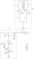
- FIG. 2 illustrates a prior art pixel sensor of the type that can be used in the imaging array shown in Figure 1 when that array is configured for a global shutter.
- Pixel 10 includes a photodiode 11 that collects the photocharge during an exposure.
- a transfer gate 12 allows the accumulated charge to be transferred from photodiode 11 to floating diffusion node 13 in response to signal T x1 .
- a floating diffusion node is defined to be an electrical node that is not tied to a power rail, or driven by another circuit.
- Floating diffusion node 13 is characterized by a parasitic capacitor 14 having a capacitance, C FD .
- the collected charge alters the voltage of floating diffusion node 13 when the charge is transferred from photodiode 11 to floating diffusion node 13.
- An optional transfer gate 15 that is controlled by a signal T x2 is used for anti-blooming protection by removing excess charge from photodiode 11 once photodiode 11 is saturated.
- a reset gate 16 is used to set the voltage on floating diffusion node 13 prior to the charge being transferred, or to reset photodiode 11 prior to an exposure.
- the voltage on floating diffusion node 13 is amplified by a source follower transistor 17.
- a signal on gate transistor 18 connects the output of source follower transistor 17 to a bit line 19 that is shared by all of the pixel sensors in a given column.
- a bit line is defined to be a conductor that is shared by a plurality of columns of pixel sensors and carries a voltage signal indicative of the voltage at the floating diffusion node in a pixel sensor that is connected to the bit line through a transfer gate.
- Each bit line terminates in a column processing circuit 28.
- Column processing circuit 28 includes an optional amplifier 21 and two sample and hold circuits whose functions will be described in more detail below.
- the first sample and hold circuit comprises switch 22 and capacitor 23, and the second sample and hold circuit comprises switch 24 and capacitor 25.
- the outputs of these sample and hold circuits are processed by a column processor 26 to provide the output value for the pixel sensor currently connected to bit line 19. The manner in which the sample and hold circuits are used will be discussed in more detail below.
- the charge in each pixel sensor is transferred to the floating diffusion node in that pixel sensor at the same time the charge is transferred in all of the other pixel sensors in the array.
- the pixel sensors are then readout row by row.
- a number of different schemes are utilized to lower the readout noise. These include correlated double sampling and correlated quadruple sampling. For the purposes of the current discussion it is sufficient to note that all of these schemes involve loading all of the floating diffusion nodes at once and then reading the rows one at a time to determine the potential on the floating diffusion nodes.
- the floating diffusion node integrates dark current that results from the parasitic photodiodes contained in the floating diffusion nodes. This dark current reduces the amount of charge that is stored on the floating diffusion node. In addition, charge stored on the floating diffusion nodes tunnels through the surrounding barriers and further reduces the charge on the floating diffusion node.
- the present invention is based on the observation that the dark current also depends on the voltage on the floating diffusion node during the period of time in which the charge is stored on the floating diffusion node. In particular, charge lost through tunneling is an exponential function of the voltage on the floating diffusion node. The charge resulting from the integration of the dark current also depends on the voltage on the floating diffusion node. Hence, if the voltage on the floating diffusion node can be reduced, the rate of charge loss from the floating diffusion node can be substantially reduced. Accordingly, the present invention provides a mechanism for lowering the voltage of the floating diffusion node during the periods in which charge is stored on the floating diffusion node and the pixel sensor is not being accessed. These periods will be referred to as storage periods in the following discussion.
- the present invention provides a circuit that reduces the voltage at the floating diffusion node in a manner that depends on a control voltage applied to a capacitor that is connected to the floating diffusion node. By switching the control voltage during the storage periods, a substantial decrease in the charge leaking off of the storage node can be achieved.
- FIG. 3 illustrates a pixel sensor according to one embodiment of the present invention.
- pixel sensor 60 includes a voltage dividing capacitor 61 that connects floating diffusion node 13 to a drive circuit 62 that sets the voltage on the lead of capacitor 61 that is not connected to floating diffusion node 13.
- D_OUT is at ground
- capacitor 61 is connected in parallel to capacitor 14 that characterizes floating diffusion node 13.
- the capacitance associated with floating diffusion node 13 is increased to the sum of the capacitances of capacitors 14 and 61. As a result, a portion of the charge that was stored on capacitor 14 moves to capacitor 61. Since floating diffusion node 13 is isolated during the storage periods, the voltage on floating diffusion node 13 is decreased by a factor equal to the ratio of the capacitance of capacitor 61, C 61 , to the sum of the capacitances of floating diffusion node 13 and capacitor 61.
- the capacitance of capacitor 61 and the voltage of D_OUT when D_OUT is high is set such that the voltage on floating diffusion node 13 during the storage periods is less than 1.5 volts but greater than 0.
- the voltage on the floating diffusion node during the storage mode is a compromise between reducing the leakage from the floating diffusion node during the storage period, while still maintaining the voltage on floating diffusion node 13 at a value greater than 0 for all possible exposure values.
- capacitor 61 could be increased to further reduce the voltage during storage; however, increasing this capacitance value decreases the sensitivity of the pixel sensor.
- the sensitivity of the pixel sensor depends on the charge to voltage conversion supplied by capacitor 14 and capacitor 61. If this capacitance is too high, the sensitivity is too low.
- capacitor 61 has a capacitance that is less than one half of that of capacitor 14.
- D_OUT is set to approximately twice V dd .
- FIG. 4A and 4B illustrate another embodiment of a pixel sensor according to the present invention.
- the additional gates are shown at 63 and 64.
- the additional transistors do not substantially increase the size of the pixel; hence, the added cost is minimal.
- the size of capacitor 61 can be reduced, or that capacitor can be eliminated.
- D_OUT is high, capacitors 65a, 65b, and 65c are connected to a high voltage by gate 63.
- gate 64 when D_OUT is at ground, gate 64 connects capacitors 65a, 65b and 65c to ground. Hence, gates 63 and 64 effectively switch capacitors 65a-c such that these capacitors are connected in parallel with capacitor 61, or in parallel with one another to the high voltage.
- C 14 is approximately 4 fF.
- C 61 is approximately half the capacitance of C 14 , i.e., 2fF.
- the capacitance of C 65c is typically the dominant capacitance for source follower transistor 17 and is approximately 1.5fF in one exemplary embodiment. Hence, C 61 could be eliminated in that embodiment.
- the goal of the arrangement shown in Figures 3 and 4 is to reduce the voltage on floating diffusion node 13 during periods in which charge is stored on floating diffusion node 13 and is waiting to be readout via source follower transistor 17. Accordingly, D_OUT is set high when floating diffusion node 13 is being reset or being readout.
- the present invention can be used advantageously in systems utilizing a global shutter in which the photodiodes in all of the pixel sensors in the array are reset at the start of an exposure and then the charge transferred to all of the floating diffusion nodes at the end of the exposure. The charge is then readout one row at a time.
- the need to transfer all of the charge at the same time while reading out the rows one at a time introduces a number of challenges in schemes that utilize multiple read operations on each pixel sensor to reduce noise in a global shutter imaging system.
- the charge integrated during an exposure on each photodiode is read by first precharging capacitor 14 associated with floating diffusion node 13 to a voltage V r with gate 12 closed and then transferring the photocharge to floating diffusion node 13 by opening gate 12.
- the difference between V r and the voltage on floating diffusion node 13 after the charge is transferred is a measure of the average light intensity at the pixel corresponding to the photodiode during the exposure.
- the reset operations are performed in parallel with the exposure part of the image formation process.
- the controller measures a reset frame.
- the photocharge is transferred to the floating diffusion nodes and an image frame is measured. The difference of the image frame and the reset frame is then used to generate the final image.
- the photodiodes are reset by opening gate 15 to connect the photodiodes to V dd and then gate 15 is closed, which starts the exposure. The exposure is terminated when gate 12 is opened to transfer the accumulated charge to floating diffusion node 13. During this exposure period, the readout circuitry is measuring the reset frame.
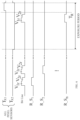
- Figure 5 illustrates the signal timings during a reset frame.
- the signals S 22 and S 24 control switches 22 and 24 shown in Figure 3 . When these signals are high, the switches are conducting. When the drive control signal, CTR, is high, D_OUT is high. When CTR is low, D_OUT is connected to ground.
- a reset frame can be viewed as consisting of two periods. During the first period of the reset frame, floating diffusion node 13 is connected to V r by causing R p to go high. This, in turn, causes the potential on the bit line to rise to its highest value. During this first period, the voltage on bit line 19 is captured on capacitor 23 by closing switch 22. Then switch 22 is again opened.
- floating diffusion node 13 is disconnected from V r by causing R p to go low, and a small decrease in the voltage on floating diffusion node 13, and hence, bit line 19 occurs.
- This new voltage is captured on capacitor 25 by closing switch 24.
- the difference between the voltages captured on capacitors 23 and 25 is then computed and becomes the reset frame value for pixel sensor 60.
- the reset frame is computed sequentially, one row at a time during the period in which the photodiodes are integrating light from the current exposure.
- the reference frame is measured while the photodiodes are integrating charge during the exposure period.
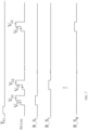
- FIG 6 illustrates the timing during the period in which the reset is being measured for the various pixel sensors in one row of the imaging array.
- the control of the exposure is set by the signals T x1 and T x2 on gates 12 and 15. These signals are the same for all of the pixel sensors in the array. Initially, T x1 is low, which isolates the photodiode in each pixel sensor from the floating diffusion node in that pixel sensor. T x1 remains low until after the reset frame is acquired. T x2 is initially high.
- the photodiode is connected to V dd and remains in a continually reset state until T x2 goes low and isolates the photodiode. This starts the exposure period.
- the exposure period terminates after the charge accumulated on the photodiode is transferred to the floating diffusion node by taking T x1 high and then low. The exposure period ends when T x1 goes low.
- All of the pixels in a given column are connected to the same bit line. As each row is connected in sequence to the bit line, the voltage on the bit line is sampled twice, once while the floating diffusion node is connected to V r and once after the floating diffusion node is disconnected from V r using gate 16. The measured voltages during these two periods are labeled as V 1r and V 2r . The column processor measures these two voltages and computes the difference of the two voltages. The difference is the reset frame pixel value for the corresponding pixel sensor. At the end of the reset period, which is shown at T R in Figure 6 , all of the floating diffusion nodes in the pixel sensors will be at the reset voltage, V 2r , measured for that floating diffusion node during the reset frame period.
- the floating diffusion node in each of the pixel sensors has a voltage determined by the V 2r value at the end of the reset frame and the charge transferred from the photodiode in that pixel sensor. This begins the data frame readout portion of the image acquisition.
- Figure 7 illustrates a data frame readout from the point of view of a bit line.
- the data frame readout begins when T x1 goes low, thus isolating the floating diffusion nodes in the pixel sensors attached to the bit line in question.
- Each pixel in the column is selected in sequence as indicated by the row select signals, R_S 1 , R_S 2 , ..., R_S n .
- V 1d the voltage on the floating diffusion node in that row is measured to provide the data value V 1d for that pixel sensor.
- the floating diffusion node is then connected at V r and the floating diffusion node voltage V 2d is measured.
- V 2d -V 1d is the pixel value for the pixel in the data frame corresponding to that pixel sensor.
- the voltage on a floating diffusion node decreases slightly when the floating diffusion node is isolated from the V r source after a reset. Hence, the value V 2d does not accurately represent the floating diffusion node voltage after reset.
- the difference in floating diffusion node voltage after isolation following a reset is, however, stored in the pixel value in the reset frame. Hence, subtracting the reset frame from the data frame pixel by pixel corrects for this difference.
- the above analysis ignores the dark current in each pixel.
- the value of V 2r at the floating diffusion node when the charge is transferred is reduced by the integrated dark current since the reset of the floating diffusion node.
- the voltage on the floating diffusion node will indicate a charge transfer that was greater than the actual charge transferred from the photodiode.
- the present invention reduces this dark current during the times the floating diffusion node is not being accessed, which are referred to as the storage periods, and hence, substantially reduces this source of error.
- FIG 8 illustrates the voltages on a floating diffusion node, V fdn , at various points in a frame.
- the pixels in the row of the pixel in question are selected for readout during the measurement of the reset frame and during the measurement of the data frame.
- the voltage on the floating diffusion node Prior to being selected for reset, the voltage on the floating diffusion node is at a value determined by the last reset during the previous data frame readout less any loss of voltage due to dark current integration. This voltage is irrelevant, since the floating diffusion node will be reset to V r as soon as the row is selected by R_S going high; however, in this example, D_OUT is set to ground.
- D_OUT goes high so that the measurements of the voltages on the floating diffusion node during and after reset can be made.
- T2 the floating diffusion node goes into a storage period until just before the charge accumulated on the photodiode during the exposure is transferred to the floating diffusion node.
- the voltage on the floating diffusion node is near that of the reset voltage, and hence, high enough to activate the parasitic photodiode in the floating diffusion node to integrate any dark current.
- D_OUT is lowered to ground, which reduces the voltage on the floating diffusion node to a value below the voltage that would allow the parasitic photodiode to integrate dark current. In one exemplary embodiment, this voltage is less than 1.5 volts.
- T3, D_OUT again goes high, and the voltage on the floating diffusion node returns to V 2r .
- the integrated charge from the photodiode is then transferred to floating diffusion node by pulsing T x1 .
- the voltage on the floating diffusion node is reduced to a value indicative of the amount of charge accumulated during the exposure period, i.e., V 1d .
- the floating diffusion node then enters another storage period during which D_OUT is again set to ground to maintain the voltage on the floating diffusion node at a value below 1.5V.
- D_OUT again goes high and the voltage on the floating diffusion node is returned to V 1d when the pixel sensor is selected for reading.
- the readout of the pixel sensor is complete.
- transfer gate 15 is used to prevent blooming and to reset the photodiode.
- an imaging array in which the pixels lack transfer gate 15 can be constructed and still function in a global shutter mode.
- the photodiode would be reset by connecting to V r through gate 16.
- the reset frame would then be computed during the exposure time as described above.
- Such an embodiment assumes that there is sufficient time to generate the reset frame during the image exposure. For short exposures, this may not be possible.
- such embodiments are not preferred because of blooming problems in pixels exposed to high light intensities. In such pixels, the photodiode can saturate, and the excess charge can leak out to contaminate nearby pixels. Gate 15 will pass the excess charge to the power rail if the voltage on the photodiode is too low, and hence, prevents such blooming.
- the above embodiments utilize a source follower transistor in each pixel sensor to generate a voltage on the bit line that is a linear function of the voltage on the floating diffusion node.
- this buffering function is accomplished with some other form of amplifier that provides a voltage on the bit line that is a monotonic function of the voltage on the floating diffusion node can also be utilized. Accordingly, the term amplifier will defined to include both source followers and other forms of amplifier within a pixel sensor.
Landscapes
- Engineering & Computer Science (AREA)
- Multimedia (AREA)
- Signal Processing (AREA)
- Solid State Image Pick-Up Elements (AREA)
- Transforming Light Signals Into Electric Signals (AREA)
Claims (11)
- Appareil comprenant une pluralité de capteurs de pixels (60, 60b) connectés à une ligne de bits, chaque capteur de pixels comprenant un premier photodétecteur comprenant :une photodiode (11) ;un noeud de diffusion flottant (13) caractérisé par une photodiode parasite et une capacité parasite ;un amplificateur (17) qui amplifie une tension sur ledit noeud de diffusion flottant pour produire un signal sur une sortie d'amplificateur ;une porte de ligne de bit (18) qui connecte ladite sortie d'amplificateur à ladite ligne de bit en réponse à un signal de sélection de rangée ;un condensateur diviseur de tension (61) ayant une première borne connectée audit noeud de diffusion flottant et une seconde borne connectée à une source d'entraînement (62) qui commute une tension sur ladite seconde borne entre un potentiel d'entraînement différent de la masse et de la masse en réponse à un signal de commande d'entraînement ;une porte de réinitialisation (16) qui connecte ledit noeud de diffusion flottant à une première source de tension de réinitialisation en réponse à un signal de réinitialisation ;une première porte de transfert (12) qui connecte ladite photodiode audit noeud de diffusion flottant en réponse à un premier signal de transfert ; etun condensateur parasite (14) pour fournir la capacité parasite au noeud de diffusion flottant, le condensateur parasite ayant une première borne connectée audit noeud de diffusion flottant, et une seconde borne connectée à la masse ;ledit amplificateur (17) comprenant un suiveur de source ayant une grille connectée audit noeud de diffusion flottant ; etledit suiveur de source ayant une borne de drain et ledit appareil étant caractérisé en ce qu'il comprend en outre un circuit de commutation qui commute ladite borne de drain d'un rail d'alimentation à la masse lorsque ladite seconde borne dudit condensateur diviseur de tension est à la masse.
- Appareil selon la revendication 1, dans lequel chaque capteur de pixel comprend en outre une seconde porte de transfert (15) qui connecte ladite photodiode à une seconde source de réinitialisation en réponse à un second signal de transfert.
- Appareil selon la revendication 1, comprenant en outre un dispositif de commande de matrice d'imagerie (70) qui génère ledit signal de sélection de rangée, ledit signal de commande d'entraînement, ledit signal de réinitialisation et ledit premier signal de porte de transfert.
- Appareil selon la revendication 3, dans lequel ledit dispositif de commande de matrice d'imagerie (70) génère ledit signal de commande d'entraînement de sorte que ladite seconde borne est à la masse et ladite sortie de l'amplificateur (17) n'est pas connectée à ladite ligne de bit en réponse audit signal de sélection de rangée.
- Appareil selon la revendication 4, dans lequel ledit dispositif de commande de matrice d'imagerie (70) génère ledit signal de commande d'entraînement de sorte que ladite seconde borne est audit potentiel d'entraînement lorsque ledit signal de réinitialisation amène ledit noeud de diffusion flottant (13) à être connecté à ladite première source de tension de réinitialisation.
- Appareil selon la revendication 4, dans lequel ledit dispositif de commande de réseau d'imagerie (70) génère ledit signal de commande d'entraînement de sorte que ladite seconde borne est audit potentiel d'entraînement lorsque ledit premier signal de transfert amène ledit noeud de diffusion flottant (13) à être connecté à ladite photodiode (11).
- Appareil selon la revendication 3 comprenant en outre un circuit de traitement de colonne (28) connecté à ladite ligne de bit, ledit circuit de traitement de colonne comprenant :un premier commutateur (22) qui connecte ladite ligne de bits à un premier condensateur d'échantillonnage et de maintien (23) en réponse à un premier signal de commande de commutateur pour générer une première tension d'échantillonnage et de maintien ;un second commutateur (24) qui connecte ladite ligne de bits à un second condensateur d'échantillonnage et de maintien (25) en réponse à un second signal de commande de commutateur pour générer une seconde tension d'échantillonnage et de maintien ; et un processeur de colonne (26) qui génère une valeur de pixel comprenant une différence entre lesdites première et seconde tensions d'échantillonnage et de maintien,ledit dispositif de commande de matrice d'imagerie (70) générant lesdits premier et second signaux de commande de commutation et recevant ladite valeur de pixel.
- Appareil selon la revendication 7, dans lequel ledit dispositif de commande de matrice d'imagerie (70) génère une valeur de pixel de trame de réinitialisation correspondant à l'un desdits capteurs de pixels (60, 60b), ladite valeur de pixel de trame de réinitialisation comprenant ladite différence desdites première et seconde tensions d'échantillonnage et de maintien, ladite première tension d'échantillonnage et de maintien correspondant audit noeud de diffusion flottant (13) étant connectée à ladite première source de réinitialisation et ladite seconde tension d'échantillonnage et de maintien correspondant audit noeud de diffusion flottant étant déconnectée de ladite première source de réinitialisation après avoir été connectée à ladite première source de réinitialisation, mais avant qu'une charge ait été transférée audit noeud de diffusion flottant après avoir été connecté à ladite première source de tension de réinitialisation.
- Appareil selon la revendication 8, dans lequel ledit dispositif de commande de matrice d'imagerie (70) génère une valeur de pixel de trame de données pour ledit un desdits capteurs de pixels (60, 60b), ladite valeur de pixel de trame de données comprenant ladite différence desdites première et seconde tensions d'échantillonnage et de maintien, ladite première tension d'échantillonnage et de maintien correspondant audit noeud de diffusion flottant (13) après qu'une charge a été transférée audit noeud de diffusion flottant depuis ladite photodiode dans ledit un desdits capteurs de pixels et ladite seconde tension d'échantillonnage et de maintien correspondant audit noeud de diffusion flottant étant connectée à ladite première source de réinitialisation après que ladite première tension d'échantillonnage et de maintien a été générée.
- Appareil selon la revendication 9, dans lequel ledit dispositif de commande de matrice d'imagerie (70) génère une valeur de pixel de trame de données corrigée à partir de ladite valeur de pixel de trame de réinitialisation et de ladite valeur de pixel de trame de données en formant une différence entre ladite valeur de pixel de trame de données et ladite valeur de pixel de trame de réinitialisation.
- Appareil selon l'une quelconque des revendications précédentes, dans lequel le condensateur diviseur de tension (61) a une capacité qui est inférieure à la moitié de la capacité du condensateur parasite (14).
Applications Claiming Priority (1)
| Application Number | Priority Date | Filing Date | Title |
|---|---|---|---|
| PCT/US2016/067618 WO2018118016A1 (fr) | 2016-12-19 | 2016-12-19 | Schéma d'obturateur global réduisant les effets d'un courant d'obscurité |
Publications (3)
| Publication Number | Publication Date |
|---|---|
| EP3556089A1 EP3556089A1 (fr) | 2019-10-23 |
| EP3556089A4 EP3556089A4 (fr) | 2020-06-10 |
| EP3556089B1 true EP3556089B1 (fr) | 2023-02-01 |
Family
ID=62627768
Family Applications (1)
| Application Number | Title | Priority Date | Filing Date |
|---|---|---|---|
| EP16924605.5A Active EP3556089B1 (fr) | 2016-12-19 | 2016-12-19 | Schéma d'obturateur global réduisant les effets d'un courant d'obscurité |
Country Status (5)
| Country | Link |
|---|---|
| US (1) | US10200644B2 (fr) |
| EP (1) | EP3556089B1 (fr) |
| CN (1) | CN110352593B (fr) |
| CA (1) | CA3047698C (fr) |
| WO (1) | WO2018118016A1 (fr) |
Families Citing this family (13)
| Publication number | Priority date | Publication date | Assignee | Title |
|---|---|---|---|---|
| US10917596B2 (en) | 2018-08-29 | 2021-02-09 | Himax Imaging Limited | Pixel circuit for generating output signals in response to incident radiation |
| JP7094455B2 (ja) | 2018-10-04 | 2022-07-01 | レイセオン カンパニー | ポンプ式大フルウェルピクセル |
| CN111565263A (zh) * | 2019-01-29 | 2020-08-21 | 广州印芯半导体技术有限公司 | 图像传感器及其像素阵列电路 |
| FR3094598A1 (fr) | 2019-03-29 | 2020-10-02 | Stmicroelectronics (Grenoble 2) Sas | Pixel et son procédé de commande |
| FR3096855B1 (fr) | 2019-06-03 | 2022-08-05 | St Microelectronics Grenoble 2 | Capteur d'image et son procédé de commande |
| FR3096856B1 (fr) | 2019-06-03 | 2021-06-25 | St Microelectronics Grenoble 2 | Capteur d'image et son procédé de commande |
| JP7393152B2 (ja) * | 2019-08-09 | 2023-12-06 | キヤノン株式会社 | 光電変換装置、撮像システム、移動体及び露光制御装置 |
| FR3103964B1 (fr) * | 2019-11-29 | 2021-11-26 | Pyxalis | Pixel à dynamique ajustable pour la réduction de bruit |
| JP7822951B2 (ja) * | 2020-11-12 | 2026-03-03 | ソニーセミコンダクタソリューションズ株式会社 | 撮像装置 |
| KR102804387B1 (ko) * | 2020-12-30 | 2025-05-07 | 에스케이하이닉스 주식회사 | 이미지 센서, 이를 이용한 이미지 센서 테스트 시스템 및 방법 |
| CN113518159B (zh) * | 2021-06-08 | 2022-11-01 | 天津大学 | 同步读出的大阵列动态视觉传感器及读出方法 |
| US12069391B2 (en) * | 2021-07-29 | 2024-08-20 | Omnivision Technologies, Inc. | Readout architectures for dark current reduction in indirect time-of-flight sensors |
| CN114384490B (zh) * | 2022-01-11 | 2025-08-29 | 上海矽印科技有限公司 | 一种激光雷达阵列全局快门 |
Family Cites Families (27)
| Publication number | Priority date | Publication date | Assignee | Title |
|---|---|---|---|---|
| JP4035194B2 (ja) * | 1996-03-13 | 2008-01-16 | キヤノン株式会社 | X線検出装置及びx線検出システム |
| KR19990084630A (ko) | 1998-05-08 | 1999-12-06 | 김영환 | 씨모스 이미지 센서 및 그 구동 방법 |
| US6459078B1 (en) * | 2000-12-04 | 2002-10-01 | Pixel Devices International, Inc. | Image sensor utilizing a low FPN high gain capacitive transimpedance amplifier |
| US7102117B2 (en) * | 2004-06-08 | 2006-09-05 | Eastman Kodak Company | Active pixel sensor cell with integrating varactor and method for using such cell |
| JP4797567B2 (ja) | 2005-10-24 | 2011-10-19 | ソニー株式会社 | 固体撮像装置、固体撮像装置の駆動方法および撮像装置 |
| US7619671B2 (en) * | 2006-07-18 | 2009-11-17 | Aptina Imaging Corporation | Method, apparatus and system for charge injection suppression in active pixel sensors |
| US20090108176A1 (en) | 2007-10-24 | 2009-04-30 | Altasens, Inc. | Global shutter pixel circuit with transistor sharing for CMOS image sensors |
| JP2009253930A (ja) * | 2008-04-11 | 2009-10-29 | Rohm Co Ltd | 光電変換装置、イメージセンサ、画像処理装置 |
| US20120211642A1 (en) * | 2009-10-27 | 2012-08-23 | Konica Minolta Opto, Inc. | Solid-State Imaging Device |
| US8294077B2 (en) * | 2010-12-17 | 2012-10-23 | Omnivision Technologies, Inc. | Image sensor having supplemental capacitive coupling node |
| JP6024103B2 (ja) | 2011-06-30 | 2016-11-09 | ソニー株式会社 | 撮像素子、撮像素子の駆動方法、撮像素子の製造方法、および電子機器 |
| TWI505453B (zh) * | 2011-07-12 | 2015-10-21 | Sony Corp | 固態成像裝置,用於驅動其之方法,用於製造其之方法,及電子裝置 |
| CN103118236B (zh) * | 2013-02-06 | 2015-09-02 | 中国航天科技集团公司第九研究院第七七一研究所 | 一种图像传感器暗电流补偿装置及补偿方法 |
| US9729808B2 (en) * | 2013-03-12 | 2017-08-08 | Tower Semiconductor Ltd. | Single-exposure high dynamic range CMOS image sensor pixel with internal charge amplifier |
| US9412782B2 (en) | 2013-07-08 | 2016-08-09 | BAE Systems Imaging Solutions Inc. | Imaging array with improved dynamic range utilizing parasitic photodiodes within floating diffusion nodes of pixels |
| US10128296B2 (en) * | 2013-07-08 | 2018-11-13 | BAE Systems Imaging Solutions Inc. | Imaging array with improved dynamic range utilizing parasitic photodiodes |
| US9374545B2 (en) * | 2013-09-13 | 2016-06-21 | BAE Systems Imaging Solutions Inc. | Amplifier adapted for CMOS imaging sensors |
| US9253396B2 (en) * | 2013-12-04 | 2016-02-02 | BAE Systems Imaging Solutions Inc. | Variable gain column amplifier adapted for use in imaging arrays |
| JP6274880B2 (ja) * | 2014-01-24 | 2018-02-07 | オリンパス株式会社 | 固体撮像装置および撮像装置 |
| JP6355387B2 (ja) * | 2014-03-31 | 2018-07-11 | キヤノン株式会社 | 撮像装置及び撮像システム |
| US9432597B2 (en) * | 2014-07-25 | 2016-08-30 | Rambus Inc. | Low-noise, high dynamic-range image sensor |
| US9832407B2 (en) * | 2014-11-26 | 2017-11-28 | Semiconductor Components Industries, Llc | Global shutter image sensor pixels having improved shutter efficiency |
| US9554074B2 (en) * | 2015-04-16 | 2017-01-24 | Omnivision Technologies, Inc. | Ramp generator for low noise image sensor |
| WO2016183091A1 (fr) * | 2015-05-11 | 2016-11-17 | Quantum Semiconductor Llc | Pixel pour utilisation avec de la lumière ayant une large plage d'intensité |
| KR20180047710A (ko) * | 2016-11-01 | 2018-05-10 | 에스케이하이닉스 주식회사 | 노이즈 제거 기능을 가지는 픽셀 바이어싱 장치 및 그에 따른 씨모스 이미지 센서 |
| US10375338B2 (en) * | 2017-02-01 | 2019-08-06 | Omnivision Technologies, Inc. | Two stage amplifier readout circuit in pixel level hybrid bond image sensors |
| CN106782325A (zh) * | 2017-03-02 | 2017-05-31 | 深圳市华星光电技术有限公司 | 像素补偿电路及驱动方法、显示装置 |
-
2016
- 2016-12-19 WO PCT/US2016/067618 patent/WO2018118016A1/fr not_active Ceased
- 2016-12-19 EP EP16924605.5A patent/EP3556089B1/fr active Active
- 2016-12-19 CN CN201680092075.4A patent/CN110352593B/zh active Active
- 2016-12-19 US US15/552,426 patent/US10200644B2/en active Active
- 2016-12-19 CA CA3047698A patent/CA3047698C/fr active Active
Also Published As
| Publication number | Publication date |
|---|---|
| CN110352593B (zh) | 2021-10-29 |
| WO2018118016A1 (fr) | 2018-06-28 |
| CN110352593A (zh) | 2019-10-18 |
| CA3047698C (fr) | 2020-03-24 |
| EP3556089A1 (fr) | 2019-10-23 |
| US20180332247A1 (en) | 2018-11-15 |
| CA3047698A1 (fr) | 2018-06-28 |
| EP3556089A4 (fr) | 2020-06-10 |
| US10200644B2 (en) | 2019-02-05 |
Similar Documents
| Publication | Publication Date | Title |
|---|---|---|
| EP3556089B1 (fr) | Schéma d'obturateur global réduisant les effets d'un courant d'obscurité | |
| JP6911128B2 (ja) | 拡張されたダイナミックレンジを備えたイメージングアレイ | |
| US8089036B2 (en) | Image sensor with global shutter and in pixel storage transistor | |
| EP4020976B1 (fr) | Réseau de pixels | |
| US8059173B2 (en) | Correlated double sampling pixel and method | |
| US20100271517A1 (en) | In-pixel correlated double sampling pixel | |
| US6590611B1 (en) | Solid-state image-pickup devices and methods for motion detection | |
| JP4288346B2 (ja) | 撮像装置及び画素回路 | |
| JP6689145B2 (ja) | 撮像装置 | |
| JP6734649B2 (ja) | 撮像装置、撮像システム、及び、撮像装置の制御方法 | |
| US10863130B2 (en) | Backside illuminated global shutter imaging array | |
| US20200335538A1 (en) | Pixel and Imaging Array with Reduced Dark Current Adapted to Low Light Imaging | |
| WO2015078780A1 (fr) | Capteur de pixels actifs et dispositif d'analyse l'utilisant | |
| HK40016059B (en) | Global shutter apparatus that reduces the effects of dark current | |
| HK40016059A (en) | Global shutter apparatus that reduces the effects of dark current | |
| Willems et al. | High-speed VGA resolution CMOS image sensor with global shutter |
Legal Events
| Date | Code | Title | Description |
|---|---|---|---|
| STAA | Information on the status of an ep patent application or granted ep patent |
Free format text: STATUS: THE INTERNATIONAL PUBLICATION HAS BEEN MADE |
|
| PUAI | Public reference made under article 153(3) epc to a published international application that has entered the european phase |
Free format text: ORIGINAL CODE: 0009012 |
|
| STAA | Information on the status of an ep patent application or granted ep patent |
Free format text: STATUS: REQUEST FOR EXAMINATION WAS MADE |
|
| 17P | Request for examination filed |
Effective date: 20190625 |
|
| AK | Designated contracting states |
Kind code of ref document: A1 Designated state(s): AL AT BE BG CH CY CZ DE DK EE ES FI FR GB GR HR HU IE IS IT LI LT LU LV MC MK MT NL NO PL PT RO RS SE SI SK SM TR |
|
| AX | Request for extension of the european patent |
Extension state: BA ME |
|
| DAV | Request for validation of the european patent (deleted) | ||
| DAX | Request for extension of the european patent (deleted) | ||
| REG | Reference to a national code |
Ref country code: DE Ref legal event code: R079 Ref document number: 602016077752 Country of ref document: DE Free format text: PREVIOUS MAIN CLASS: H04N0005341000 Ipc: H04N0005361000 |
|
| STAA | Information on the status of an ep patent application or granted ep patent |
Free format text: STATUS: EXAMINATION IS IN PROGRESS |
|
| A4 | Supplementary search report drawn up and despatched |
Effective date: 20200513 |
|
| RIC1 | Information provided on ipc code assigned before grant |
Ipc: H04N 5/357 20110101ALI20200507BHEP Ipc: H04N 5/361 20110101AFI20200507BHEP Ipc: H04N 5/3745 20110101ALI20200507BHEP |
|
| 17Q | First examination report despatched |
Effective date: 20200604 |
|
| GRAP | Despatch of communication of intention to grant a patent |
Free format text: ORIGINAL CODE: EPIDOSNIGR1 |
|
| STAA | Information on the status of an ep patent application or granted ep patent |
Free format text: STATUS: GRANT OF PATENT IS INTENDED |
|
| INTG | Intention to grant announced |
Effective date: 20220920 |
|
| RIN1 | Information on inventor provided before grant (corrected) |
Inventor name: MIMS, STEPHEN W. Inventor name: LIM, PAUL G. Inventor name: DO, HUNG T. |
|
| GRAS | Grant fee paid |
Free format text: ORIGINAL CODE: EPIDOSNIGR3 |
|
| GRAA | (expected) grant |
Free format text: ORIGINAL CODE: 0009210 |
|
| STAA | Information on the status of an ep patent application or granted ep patent |
Free format text: STATUS: THE PATENT HAS BEEN GRANTED |
|
| AK | Designated contracting states |
Kind code of ref document: B1 Designated state(s): AL AT BE BG CH CY CZ DE DK EE ES FI FR GB GR HR HU IE IS IT LI LT LU LV MC MK MT NL NO PL PT RO RS SE SI SK SM TR |
|
| REG | Reference to a national code |
Ref country code: GB Ref legal event code: FG4D |
|
| REG | Reference to a national code |
Ref country code: CH Ref legal event code: EP Ref country code: AT Ref legal event code: REF Ref document number: 1547216 Country of ref document: AT Kind code of ref document: T Effective date: 20230215 |
|
| REG | Reference to a national code |
Ref country code: DE Ref legal event code: R096 Ref document number: 602016077752 Country of ref document: DE |
|
| REG | Reference to a national code |
Ref country code: IE Ref legal event code: FG4D |
|
| REG | Reference to a national code |
Ref country code: LT Ref legal event code: MG9D |
|
| REG | Reference to a national code |
Ref country code: NL Ref legal event code: MP Effective date: 20230201 |
|
| REG | Reference to a national code |
Ref country code: AT Ref legal event code: MK05 Ref document number: 1547216 Country of ref document: AT Kind code of ref document: T Effective date: 20230201 |
|
| PG25 | Lapsed in a contracting state [announced via postgrant information from national office to epo] |
Ref country code: RS Free format text: LAPSE BECAUSE OF FAILURE TO SUBMIT A TRANSLATION OF THE DESCRIPTION OR TO PAY THE FEE WITHIN THE PRESCRIBED TIME-LIMIT Effective date: 20230201 Ref country code: PT Free format text: LAPSE BECAUSE OF FAILURE TO SUBMIT A TRANSLATION OF THE DESCRIPTION OR TO PAY THE FEE WITHIN THE PRESCRIBED TIME-LIMIT Effective date: 20230601 Ref country code: NO Free format text: LAPSE BECAUSE OF FAILURE TO SUBMIT A TRANSLATION OF THE DESCRIPTION OR TO PAY THE FEE WITHIN THE PRESCRIBED TIME-LIMIT Effective date: 20230501 Ref country code: NL Free format text: LAPSE BECAUSE OF FAILURE TO SUBMIT A TRANSLATION OF THE DESCRIPTION OR TO PAY THE FEE WITHIN THE PRESCRIBED TIME-LIMIT Effective date: 20230201 Ref country code: LV Free format text: LAPSE BECAUSE OF FAILURE TO SUBMIT A TRANSLATION OF THE DESCRIPTION OR TO PAY THE FEE WITHIN THE PRESCRIBED TIME-LIMIT Effective date: 20230201 Ref country code: LT Free format text: LAPSE BECAUSE OF FAILURE TO SUBMIT A TRANSLATION OF THE DESCRIPTION OR TO PAY THE FEE WITHIN THE PRESCRIBED TIME-LIMIT Effective date: 20230201 Ref country code: HR Free format text: LAPSE BECAUSE OF FAILURE TO SUBMIT A TRANSLATION OF THE DESCRIPTION OR TO PAY THE FEE WITHIN THE PRESCRIBED TIME-LIMIT Effective date: 20230201 Ref country code: ES Free format text: LAPSE BECAUSE OF FAILURE TO SUBMIT A TRANSLATION OF THE DESCRIPTION OR TO PAY THE FEE WITHIN THE PRESCRIBED TIME-LIMIT Effective date: 20230201 Ref country code: AT Free format text: LAPSE BECAUSE OF FAILURE TO SUBMIT A TRANSLATION OF THE DESCRIPTION OR TO PAY THE FEE WITHIN THE PRESCRIBED TIME-LIMIT Effective date: 20230201 |
|
| PG25 | Lapsed in a contracting state [announced via postgrant information from national office to epo] |
Ref country code: SE Free format text: LAPSE BECAUSE OF FAILURE TO SUBMIT A TRANSLATION OF THE DESCRIPTION OR TO PAY THE FEE WITHIN THE PRESCRIBED TIME-LIMIT Effective date: 20230201 Ref country code: PL Free format text: LAPSE BECAUSE OF FAILURE TO SUBMIT A TRANSLATION OF THE DESCRIPTION OR TO PAY THE FEE WITHIN THE PRESCRIBED TIME-LIMIT Effective date: 20230201 Ref country code: IS Free format text: LAPSE BECAUSE OF FAILURE TO SUBMIT A TRANSLATION OF THE DESCRIPTION OR TO PAY THE FEE WITHIN THE PRESCRIBED TIME-LIMIT Effective date: 20230601 Ref country code: GR Free format text: LAPSE BECAUSE OF FAILURE TO SUBMIT A TRANSLATION OF THE DESCRIPTION OR TO PAY THE FEE WITHIN THE PRESCRIBED TIME-LIMIT Effective date: 20230502 Ref country code: FI Free format text: LAPSE BECAUSE OF FAILURE TO SUBMIT A TRANSLATION OF THE DESCRIPTION OR TO PAY THE FEE WITHIN THE PRESCRIBED TIME-LIMIT Effective date: 20230201 |
|
| PG25 | Lapsed in a contracting state [announced via postgrant information from national office to epo] |
Ref country code: SM Free format text: LAPSE BECAUSE OF FAILURE TO SUBMIT A TRANSLATION OF THE DESCRIPTION OR TO PAY THE FEE WITHIN THE PRESCRIBED TIME-LIMIT Effective date: 20230201 Ref country code: RO Free format text: LAPSE BECAUSE OF FAILURE TO SUBMIT A TRANSLATION OF THE DESCRIPTION OR TO PAY THE FEE WITHIN THE PRESCRIBED TIME-LIMIT Effective date: 20230201 Ref country code: EE Free format text: LAPSE BECAUSE OF FAILURE TO SUBMIT A TRANSLATION OF THE DESCRIPTION OR TO PAY THE FEE WITHIN THE PRESCRIBED TIME-LIMIT Effective date: 20230201 Ref country code: DK Free format text: LAPSE BECAUSE OF FAILURE TO SUBMIT A TRANSLATION OF THE DESCRIPTION OR TO PAY THE FEE WITHIN THE PRESCRIBED TIME-LIMIT Effective date: 20230201 Ref country code: CZ Free format text: LAPSE BECAUSE OF FAILURE TO SUBMIT A TRANSLATION OF THE DESCRIPTION OR TO PAY THE FEE WITHIN THE PRESCRIBED TIME-LIMIT Effective date: 20230201 |
|
| REG | Reference to a national code |
Ref country code: DE Ref legal event code: R097 Ref document number: 602016077752 Country of ref document: DE |
|
| PG25 | Lapsed in a contracting state [announced via postgrant information from national office to epo] |
Ref country code: SK Free format text: LAPSE BECAUSE OF FAILURE TO SUBMIT A TRANSLATION OF THE DESCRIPTION OR TO PAY THE FEE WITHIN THE PRESCRIBED TIME-LIMIT Effective date: 20230201 |
|
| PLBE | No opposition filed within time limit |
Free format text: ORIGINAL CODE: 0009261 |
|
| STAA | Information on the status of an ep patent application or granted ep patent |
Free format text: STATUS: NO OPPOSITION FILED WITHIN TIME LIMIT |
|
| 26N | No opposition filed |
Effective date: 20231103 |
|
| PG25 | Lapsed in a contracting state [announced via postgrant information from national office to epo] |
Ref country code: SI Free format text: LAPSE BECAUSE OF FAILURE TO SUBMIT A TRANSLATION OF THE DESCRIPTION OR TO PAY THE FEE WITHIN THE PRESCRIBED TIME-LIMIT Effective date: 20230201 |
|
| REG | Reference to a national code |
Ref country code: DE Ref legal event code: R119 Ref document number: 602016077752 Country of ref document: DE |
|
| REG | Reference to a national code |
Ref country code: CH Ref legal event code: PL |
|
| PG25 | Lapsed in a contracting state [announced via postgrant information from national office to epo] |
Ref country code: LU Free format text: LAPSE BECAUSE OF NON-PAYMENT OF DUE FEES Effective date: 20231219 |
|
| PG25 | Lapsed in a contracting state [announced via postgrant information from national office to epo] |
Ref country code: MC Free format text: LAPSE BECAUSE OF FAILURE TO SUBMIT A TRANSLATION OF THE DESCRIPTION OR TO PAY THE FEE WITHIN THE PRESCRIBED TIME-LIMIT Effective date: 20230201 |
|
| REG | Reference to a national code |
Ref country code: BE Ref legal event code: MM Effective date: 20231231 |
|
| PG25 | Lapsed in a contracting state [announced via postgrant information from national office to epo] |
Ref country code: MC Free format text: LAPSE BECAUSE OF FAILURE TO SUBMIT A TRANSLATION OF THE DESCRIPTION OR TO PAY THE FEE WITHIN THE PRESCRIBED TIME-LIMIT Effective date: 20230201 Ref country code: LU Free format text: LAPSE BECAUSE OF NON-PAYMENT OF DUE FEES Effective date: 20231219 |
|
| REG | Reference to a national code |
Ref country code: IE Ref legal event code: MM4A |
|
| PG25 | Lapsed in a contracting state [announced via postgrant information from national office to epo] |
Ref country code: DE Free format text: LAPSE BECAUSE OF NON-PAYMENT OF DUE FEES Effective date: 20240702 Ref country code: IE Free format text: LAPSE BECAUSE OF NON-PAYMENT OF DUE FEES Effective date: 20231219 |
|
| PG25 | Lapsed in a contracting state [announced via postgrant information from national office to epo] |
Ref country code: BE Free format text: LAPSE BECAUSE OF NON-PAYMENT OF DUE FEES Effective date: 20231231 |
|
| PG25 | Lapsed in a contracting state [announced via postgrant information from national office to epo] |
Ref country code: CH Free format text: LAPSE BECAUSE OF NON-PAYMENT OF DUE FEES Effective date: 20231231 |
|
| PG25 | Lapsed in a contracting state [announced via postgrant information from national office to epo] |
Ref country code: IE Free format text: LAPSE BECAUSE OF NON-PAYMENT OF DUE FEES Effective date: 20231219 Ref country code: DE Free format text: LAPSE BECAUSE OF NON-PAYMENT OF DUE FEES Effective date: 20240702 Ref country code: CH Free format text: LAPSE BECAUSE OF NON-PAYMENT OF DUE FEES Effective date: 20231231 Ref country code: BE Free format text: LAPSE BECAUSE OF NON-PAYMENT OF DUE FEES Effective date: 20231231 |
|
| PG25 | Lapsed in a contracting state [announced via postgrant information from national office to epo] |
Ref country code: BG Free format text: LAPSE BECAUSE OF FAILURE TO SUBMIT A TRANSLATION OF THE DESCRIPTION OR TO PAY THE FEE WITHIN THE PRESCRIBED TIME-LIMIT Effective date: 20230201 |
|
| PG25 | Lapsed in a contracting state [announced via postgrant information from national office to epo] |
Ref country code: BG Free format text: LAPSE BECAUSE OF FAILURE TO SUBMIT A TRANSLATION OF THE DESCRIPTION OR TO PAY THE FEE WITHIN THE PRESCRIBED TIME-LIMIT Effective date: 20230201 |
|
| PGFP | Annual fee paid to national office [announced via postgrant information from national office to epo] |
Ref country code: FR Payment date: 20250225 Year of fee payment: 9 |
|
| PGFP | Annual fee paid to national office [announced via postgrant information from national office to epo] |
Ref country code: IT Payment date: 20250220 Year of fee payment: 9 |
|
| PG25 | Lapsed in a contracting state [announced via postgrant information from national office to epo] |
Ref country code: CY Free format text: LAPSE BECAUSE OF FAILURE TO SUBMIT A TRANSLATION OF THE DESCRIPTION OR TO PAY THE FEE WITHIN THE PRESCRIBED TIME-LIMIT; INVALID AB INITIO Effective date: 20161219 |
|
| PG25 | Lapsed in a contracting state [announced via postgrant information from national office to epo] |
Ref country code: HU Free format text: LAPSE BECAUSE OF FAILURE TO SUBMIT A TRANSLATION OF THE DESCRIPTION OR TO PAY THE FEE WITHIN THE PRESCRIBED TIME-LIMIT; INVALID AB INITIO Effective date: 20161219 |
|
| PG25 | Lapsed in a contracting state [announced via postgrant information from national office to epo] |
Ref country code: TR Free format text: LAPSE BECAUSE OF FAILURE TO SUBMIT A TRANSLATION OF THE DESCRIPTION OR TO PAY THE FEE WITHIN THE PRESCRIBED TIME-LIMIT Effective date: 20230201 |
|
| PGFP | Annual fee paid to national office [announced via postgrant information from national office to epo] |
Ref country code: GB Payment date: 20251229 Year of fee payment: 10 |