EP3556020B1 - Hörhilfevorrichtung mit geteilter stromversorgungsspannung als spannungsreferenz - Google Patents
Hörhilfevorrichtung mit geteilter stromversorgungsspannung als spannungsreferenz Download PDFInfo
- Publication number
- EP3556020B1 EP3556020B1 EP16820203.4A EP16820203A EP3556020B1 EP 3556020 B1 EP3556020 B1 EP 3556020B1 EP 16820203 A EP16820203 A EP 16820203A EP 3556020 B1 EP3556020 B1 EP 3556020B1
- Authority
- EP
- European Patent Office
- Prior art keywords
- voltage
- reference voltage
- output
- power supply
- input
- Prior art date
- Legal status (The legal status is an assumption and is not a legal conclusion. Google has not performed a legal analysis and makes no representation as to the accuracy of the status listed.)
- Active
Links
Images

Classifications
-
- H—ELECTRICITY
- H04—ELECTRIC COMMUNICATION TECHNIQUE
- H04R—LOUDSPEAKERS, MICROPHONES, GRAMOPHONE PICK-UPS OR LIKE ACOUSTIC ELECTROMECHANICAL TRANSDUCERS; DEAF-AID SETS; PUBLIC ADDRESS SYSTEMS
- H04R25/00—Deaf-aid sets, i.e. electro-acoustic or electro-mechanical hearing aids; Electric tinnitus maskers providing an auditory perception
- H04R25/50—Customised settings for obtaining desired overall acoustical characteristics
- H04R25/505—Customised settings for obtaining desired overall acoustical characteristics using digital signal processing
-
- H—ELECTRICITY
- H03—ELECTRONIC CIRCUITRY
- H03M—CODING; DECODING; CODE CONVERSION IN GENERAL
- H03M3/00—Conversion of analogue values to or from differential modulation
- H03M3/30—Delta-sigma modulation
- H03M3/322—Continuously compensating for, or preventing, undesired influence of physical parameters
- H03M3/368—Continuously compensating for, or preventing, undesired influence of physical parameters of noise other than the quantisation noise already being shaped inherently by delta-sigma modulators
-
- H—ELECTRICITY
- H03—ELECTRONIC CIRCUITRY
- H03M—CODING; DECODING; CODE CONVERSION IN GENERAL
- H03M3/00—Conversion of analogue values to or from differential modulation
- H03M3/30—Delta-sigma modulation
- H03M3/458—Analogue/digital converters using delta-sigma modulation as an intermediate step
-
- H—ELECTRICITY
- H04—ELECTRIC COMMUNICATION TECHNIQUE
- H04R—LOUDSPEAKERS, MICROPHONES, GRAMOPHONE PICK-UPS OR LIKE ACOUSTIC ELECTROMECHANICAL TRANSDUCERS; DEAF-AID SETS; PUBLIC ADDRESS SYSTEMS
- H04R25/00—Deaf-aid sets, i.e. electro-acoustic or electro-mechanical hearing aids; Electric tinnitus maskers providing an auditory perception
- H04R25/45—Prevention of acoustic reaction, i.e. acoustic oscillatory feedback
- H04R25/453—Prevention of acoustic reaction, i.e. acoustic oscillatory feedback electronically
-
- H—ELECTRICITY
- H04—ELECTRIC COMMUNICATION TECHNIQUE
- H04R—LOUDSPEAKERS, MICROPHONES, GRAMOPHONE PICK-UPS OR LIKE ACOUSTIC ELECTROMECHANICAL TRANSDUCERS; DEAF-AID SETS; PUBLIC ADDRESS SYSTEMS
- H04R2225/00—Details of deaf aids covered by H04R25/00, not provided for in any of its subgroups
- H04R2225/33—Aspects relating to adaptation of the battery voltage, e.g. its regulation, increase or decrease
-
- H—ELECTRICITY
- H04—ELECTRIC COMMUNICATION TECHNIQUE
- H04R—LOUDSPEAKERS, MICROPHONES, GRAMOPHONE PICK-UPS OR LIKE ACOUSTIC ELECTROMECHANICAL TRANSDUCERS; DEAF-AID SETS; PUBLIC ADDRESS SYSTEMS
- H04R2225/00—Details of deaf aids covered by H04R25/00, not provided for in any of its subgroups
- H04R2225/43—Signal processing in hearing aids to enhance the speech intelligibility
Definitions
- the present invention relates to hearing assistive devices.
- the invention more particularly, relates to a hearing assistive device with increased dynamic input range.
- the invention relates to a voltage supply for an analog-to-digital converter.
- the dynamic input range is a prerequisite for ensuring a true reproduction of natural sounds.
- the presence of sounds exceeding the the dynamic range of the input stage causes the signal to be clipped, which results in distorting harmonics present in the signal to be processed.
- Patent application WO 2007/120400 Al teaches a delta-sigma modulator that can be used in audio signal applications, where in the reference voltage is a scaled version of the power supply voltage.
- Patent application US 2008/291069 Al presents a delta-sigma modulator that can be used in digital audio equipment, where in the reference voltage is a buffered scaled version of the power supply voltage.
- the purpose of the invention is to provide a hearing assistive device or a hearing aid with increased dynamic input range ensuring the reproduction of natural sounds.
- the achievable dynamic range from a hearing can be increased.
- the increased dynamic range provides artifact-free sound processing even in even louder sound environments, and thereby improved speech intelligibility in loud sound environments.
- fig. 1 schematically illustrates a delta sigma converter 10 in which a reference voltage generation circuit according to one embodiment of the invention may implemented.
- the delta sigma converter 10 converts an analog voltage or analog signal 13 received on an input 11 into a digital representation 14 delivered on an output 12.
- the digital representation 14 is known as Pulse Density modulation or Pulse Frequency modulation.
- frequency may vary smoothly in infinitesimal steps, as may voltage, and both may serve as an analog of an infinitesimally varying physical variable such as a speech signal or an acoustic signal.
- the substitution of frequency for voltage is thus entirely natural and carries in its train the transmission advantages of a pulse stream.
- A/D converters including the delta sigma converter 10
- the input voltage to the A/D converter is measured relative to this reference voltage. Hence, it is important that the reference voltage has sufficiently low noise.
- the delta sigma converter 10 converts the mean of the analog voltage into the mean of the analog pulse frequency and counts the pulses in a known interval so that the pulse count divided by the interval gives an accurate digital representation of the mean analog voltage during the interval.
- This interval can be chosen to give any desired resolution or accuracy.
- Fig. 2 illustrates schematically a hearing assistive device according to an embodiment of the invention.
- the hearing assistive device includes an example of an A/D converter. This converter is a 1-bit time-continuous delta sigma converter of first order, but the principles according to the invention applies to all converter types.
- the hearing assistive device may be a hearing aid.
- the hearing assistive device has at least one input transducer or microphone 18 picking up an audio signal and transforming it into an electric representation, e.g. the analog signal 13.
- the delta sigma converter 10 receives the analog signal 13 at the input 11.
- the delta sigma converter 10 comprises an input transformer 19 receiving the analog signal 13 and outputting a transformed voltage to a summation point 20.
- the input transformer 19 includes a switchable capacitor configuration which may be operated as described later with reference to fig. 4 .
- a feedback voltage from a feedback loop is subtracted from the transformed voltage in the summation point 20, and the resulting signal is supplied to an integrator 21 performing a time integration of the signal voltage from the summation point 20.
- the integrator 21 will have a low pass filtering effect.
- the integral signal provided as the output from the integrator 21 will increase or decrease depending on whether the signal voltage from the summation point 20 is positive or negative.
- the integral signal from the integrator 21 is presented to the input of a comparator 22 for generating a logical "1"-level whenever the integral signal exceeds a reference voltage V ref presented to the comparator 22, and a logical "0"-level whenever the integral signal from the integrator 21 is below the reference voltage V ref .
- the reference voltage V ref is adapted to be lower than the power supply voltage provided by the battery voltage V battery and to follow the decay of the battery voltage V battery with a predefined margin.
- This predefined margin may in one embodiment be lower than 10% of the battery voltage V battery .
- This predefined margin may in a further embodiment be lower than 5% of the battery voltage V battery .
- the binary output from the comparator 22 feeds the data input of a D flip-flop 24.
- the D flip-flop 24 captures the value of the D-input at a definite portion of the clock cycle, such as the rising edge of a clock signal. That captured value of the D-input becomes the Q output until the next definite portion of the clock cycle occurs and a new value of the D-input is captured and becomes the next Q output.
- the clock frequency of the clock signal from a clock signal generator 25 defines the bit rate of the output signal 14 from the delta sigma converter 10.
- the clock frequency is stable in the range of 1 - 2 MHz.
- a charging and discharging period of the input transformer 19 may correspond to e.g. 64 clock cycles from the clock signal generator 25.
- the bit stream from the flip-flop 24 is provided at the output 12 of the delta sigma converter 10 as a digital audio signal to a digital signal processor 27.
- the digital signal processor 27 is preferably a specialized microprocessor with its architecture optimized for the operational needs of digital signal processing, and in the illustrated embodiment the processor 27 is adapted for amplifying and conditioning of the audio signal intended to become presented for the hearing aid user.
- the amplification and conditioning is carried out according to a predetermined setting in order to alleviate a hearing loss by amplifying sound at frequencies in those parts of the audible frequency range where the user suffers a hearing deficit.
- the processor 27 outputs according to one embodiment of the invention a digital signal fed to a digital output stage 28 and an output transducer or a speaker 29.
- the speaker 29 may be driven as a class D amplifier by the one-bit digital data stream received.
- the output 12 of the delta sigma converter 10 is branched to provide a part of the data stream to a feedback loop.
- the part of the data stream is forwarded to a 1-bit D/A converter 26 converting the logical ones and zeroes in the part of the data stream into a positive or negative voltage with respect to the transformed voltage for subtraction from the transformed voltage in the summation point 20.
- the gain in the A/D converter or the delta sigma converter 10 is inversely proportional to the reference voltage, V ref . This is opposite to the output stage 28, which has a gain proportional to the reference voltage, V ref .
- the entire hearing aid or hearing assistive device is neutral in relation to the reference voltage, V ref , and we thereby obtain an additional advantage using a reference voltage, V ref , following the decay of the power supply voltage V battery with a predefined margin.
- the reference voltage generation circuit 23 is shown in fig. 3 .
- the reference voltage generation circuit 23 is adapted to provide a reference voltage V ref from a power supply V battery , which may be hearing aid battery cell, e.g. of type 312 (discharge curve indicated in fig. 5 .
- the reference voltage generation circuit 23 comprises an electronic voltage amplifier or op-amp being coupled to the power supply V battery via a passive circuit.
- the electronic voltage amplifier (op-amp) outputs the reference voltage V ref .
- the reference voltage generation circuit 23 is adapted to control the reference voltage V ref to be lower than the power supply V battery and to follow the decay of the power supply V battery with a predefined margin ⁇ V.
- the passive circuit of the reference voltage generation circuit 23 includes two resistors R 1 and R 2 providing a first voltage divider.
- the first voltage divider in the illustrated embodiment is a simple configuration with two resistors connected in series, with the input voltage V battery applied across the resistor pair and the output voltage emerging or being tapped from the connection between them.
- the output voltage from the first voltage divider is connected to a first input terminal of the electronic voltage amplifier via a low pass filter provided by a diode Di and a capacitor C 1 .
- the low pass filter removes noise originating from the power supply, and prevents rapid changes of the voltage that would generate audible artifacts.
- V ref V battery * 1 + R 3 / R 4 / 1 + R 1 / R 2
- the reference voltage V ref must be less than the battery supply V battery so the gain must be configured so that 1 + R 3 / R 4 / 1 + R 1 / R 2 ⁇ 1
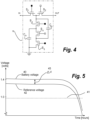
- Fig. 4 shows how the input transformer 19 is operated in two phases; a charging phase and a discharging phase.
- the analog signal 13 (see fig. 1 ) is charging two capacitors, C a and C b , arranged in parallel, while the same two capacitors, C a and C b , are switched into series in the discharging phase and being connected to OUT or the summation point 20.
- the benefit by switching the capacitor coupling between parallel and series coupling is that the voltage supplied to the summation point 20 when switching to discharge phase is doubled and subsequently the discharging is twice as fast. This is beneficial as the relative noise voltage level is reduced without the need for increasing the supply current to the amplifier in the delta sigma converter 10.
- Five switching transistor S 1 - S 5 are controlled by a sampling clock signal (not shown) where the signal edge of the clock signal goes positive in the charging phase, the switching transistors S 1 , S 3 , and S 5 close, and S 2 and S 4 open.
- the switching transistors S 1 , S 3 , and S 5 of the input transformer 19 open, and the switching transistors S 2 and S 4 close.
- Table 1 S 1 , S 3 , S 5 S 2 , S 4 Charging phase Closed Open C a and C b are connected in parallel Discharging phase Open Closed C a and C b are connected in series
- the filled and unfilled squares at the gate of the switching transistor S 1 - S 5 indicate the operation of the switch.
- a filled square denotes a closed transistor switch in the charging phase and an open transistor switch in the discharging phase.
- An unfilled square denotes an open transistor switch in the charging phase and a closed transistor switch in the discharging phase.
- the noise generated from the A/D converter or the delta sigma converter will be substantially independent of the reference voltage.
- the reason for this is that the inherent thermal noises from amplifiers etc. are the dominant noise sources independent of the reference voltage.
- the A/D converter or the delta sigma converter will have benefits of having as high reference voltage as possible in order to increase the achievable dynamic range.
- the range for the input voltage for the converter increases, but the noise remains constant.
- this means that with a suitable microphone the hearing aid will be able to handle a larger dynamic range.
- the reference voltage according to the invention may be used as supply not only for the A/D converter or the delta sigma converter. Similar to the A/D converter or the delta sigma converter, some microphone types applicable for use in the hearing aid or a hearing assistive device may benefit from an increased reference voltage for improving the dynamic range.
- Fig. 5 illustrates (voltage versus time) how the voltage 40 from a hearing aid battery (type 312) varies during its lifetime. It typically starts out at a voltage up to 1.4 Volts, but the voltage can decrease to less than 1.0 volts before the battery is no longer able to power the hearing aid or the hearing assistive device. Therefore, the reference value has traditionally been decided to be fixed at a level just below the voltage at which the battery is no longer able to power the hearing aid or a hearing assistive device allowing at least 50mV of voltage headroom for noise removal.
- the reference voltage generation circuit is adapted to provide a reference voltage V ref which is lower than a power supply voltage V battery and following the decay of the power supply voltage V battery with a predefined margin.
- the reference voltage V ref is supplied to the A/D converters and microphones. This may increase the achievable dynamic range during most of the battery's lifetime.
- the reference voltage generation circuit 23 provides a reference voltage V ref from a power supply V battery .
- the reference voltage generation circuit is adapted to control the reference voltage V ref (the curve 42) to be lower than the power supply V battery (the curve 40) and to follow the decay of the power supply V battery with a predefined margin ⁇ V (the difference 43).
- the level 41 is indicated on the figure as the level traditionally used to power the A/D converter and ensuring quiet and noise free reference voltage.
Landscapes
- Engineering & Computer Science (AREA)
- Theoretical Computer Science (AREA)
- Health & Medical Sciences (AREA)
- General Health & Medical Sciences (AREA)
- Neurosurgery (AREA)
- Otolaryngology (AREA)
- Physics & Mathematics (AREA)
- Acoustics & Sound (AREA)
- Signal Processing (AREA)
- Compression, Expansion, Code Conversion, And Decoders (AREA)
Claims (3)
- Hörhilfevorrichtung, die eine Audioverarbeitungsschaltung beinhaltet, umfassend:- einen Delta-Sigma-Analog-Digital-Wandler, der Folgendes aufweist:- einen analogen Eingang, der ein Audiosignal ist;- einen Integrator, der verbunden ist, um eine Spannung, die an einem Summationspunkt vorhanden ist, der mit dem Eingangssignal gekoppelt ist, zu integrieren;- einen Komparator, der verbunden ist, um einen Spannungsausgang vom Integrator mit einer Referenzspannung (Vref) zu vergleichen und Ausgeben eines Logikpegels in Übereinstimmung mit dem Vergleich;- ein Flip-Flop, das verbunden ist, um den Komparatorausgang zu verriegeln;- eine Rückkopplungsschleife, die ein Rückkopplungssignal zum Summationspunkt rückkoppelt; und die Rückkopplungsschleife einen DA-Wandler umfasst, der den verriegelten Komparatorausgang verwendet, um ein Rückkopplungssignal zu erzeugen; und- eine Stromversorgungsspannung (VBatterie), die von einer Batterie bereitgestellt wird, die während des Entladens ein Abklingen zeigt;- wobei eine Schaltung zum Erzeugen einer Referenzspannung angepasst ist, um die Referenzspannung (Vref) auf einem Spannungspegel bereitzustellen, der niedriger ist als jener der Stromversorgungsspannung (VBatterie), und um dem Abklingen der Stromversorgungsspannung (VBatterie) mit einer vordefinierten Spanne zu folgen;wobei die Schaltung zum Erzeugen einer Referenzspannung umfasst:- eine Tiefpassfilterschaltung, die eine Diode (D1) und einen Kondensator (C1) umfasst, die angeordnet sind, um Rauschen, das von der Stromversorgung stammt, zu entfernen, wobei der Kondensator zwischen der Kathode der Diode und Masse verbunden ist;- einen ersten Spannungsteiler (R1, R2), der zwischen der Stromversorgungsspannung (VBatterie) und Masse verbunden ist, wobei der Ausgang vom ersten Spannungsteiler (R1, R2) mit der Anode der Diode verbunden ist;- einen elektronischen Spannungsverstärker (Operationsverstärker), um die Referenzspannung (Vref) auszugeben, und mit einem ersten Eingang, der mit der Kathode der Diode verbunden ist; und- einen zweiten Spannungsteiler (R3, R4), der zwischen der Referenzspannung (Vref) und Masse verbunden ist, wobei der Ausgang vom zweiten Spannungsteiler (R3, R4) mit einem zweiten Eingangsanschluss des elektronischen Spannungsverstärkers (Operationsverstärker) verbunden ist.
- Hörhilfevorrichtung nach Anspruch 1, wobei der elektronische Spannungsverstärker (Operationsverstärker) ein gleichstromgekoppelter elektronischer Spannungsverstärker mit hoher Verstärkung mit einem Eingang und einem unsymmetrischen Ausgang ist, der die Referenzspannung (Vref) darstellt.
- Verfahren zum Verarbeiten von Audio in einer Hörhilfevorrichtung, und die Schritte umfassend zum:- Umwandeln eines analogen Signals von einem Mikrofon in einem Analog-Digital-Wandler; wobei der Analog-Digital-Wandler ein Delta-Sigma-Wandler ist, der einen Komparator aufweist,- Vergleichen eines Ausgangs von einem Integrator mit der Referenzspannung (Vref), wobei der Integrator eine Spannung, die an einem Summationspunkt vorhanden ist, der mit dem Eingangssignal und einem Rückkopplungssignal gekoppelt ist, integriert, und- Ausgeben eines Logikpegels in Übereinstimmung mit dem Vergleich,- Verriegeln des Ausgangs des Komparators durch ein Flip-Flop; und- Verwenden des verriegelten Komparatorausgangs als Eingang eines DA-Wandlers, um das Rückkopplungssignal zu erzeugen;wobei das Verfahren weiter die Schritte umfasst zum:- Erzeugen einer Referenzspannung (Vref) aus einer Stromversorgungsspannung (VBatterie); wobei die Stromversorgungsspannung (VBatterie) von einer Batterie bereitgestellt wird, die beim Entladen ein Abklingen zeigt;- wobei die Referenzspannung (Vref) niedriger ist als die Stromversorgungsspannung (VBatterie) und dem Abklingen der Stromversorgungsspannung (VBatterie) mit einer vordefinierten Spanne folgt, wobei das Erzeugen der Referenzspannung die Schritte umfasst zum:- Filtern des Ausgangs eines ersten Spannungsteilers (R1, R2), der zwischen der Stromversorgungsspannung und Masse verbunden ist, durch eine Tiefpassfilterschaltung, die eine Diode (D1) und einen Kondensator (C1) umfasst, die angeordnet sind, um Rauschen, das von der Stromversorgung stammt, zu entfernen, wobei der Kondensator zwischen der Kathode der Diode und Masse verbunden ist;- Puffern und Skalieren des Filterausgangs durch einen elektronischen Spannungsverstärker (Operationsverstärker) und einen zweiten Spannungsteiler (R3, R4), der zwischen der Referenzspannung (Vref) und Masse verbunden ist, wobei der Ausgang vom zweiten Spannungsteiler (R3, R4) mit einem Eingangsanschluss des elektronischen Spannungsverstärkers (Operationsverstärker) verbunden ist;- Bereitstellen der Referenzspannung am Ausgang des elektronischen Spannungsverstärkers.
Applications Claiming Priority (1)
| Application Number | Priority Date | Filing Date | Title |
|---|---|---|---|
| PCT/EP2016/080925 WO2018108260A1 (en) | 2016-12-14 | 2016-12-14 | A hearing assistive device with a divided power supply voltage as voltage reference |
Publications (3)
| Publication Number | Publication Date |
|---|---|
| EP3556020A1 EP3556020A1 (de) | 2019-10-23 |
| EP3556020C0 EP3556020C0 (de) | 2025-02-12 |
| EP3556020B1 true EP3556020B1 (de) | 2025-02-12 |
Family
ID=57708553
Family Applications (1)
| Application Number | Title | Priority Date | Filing Date |
|---|---|---|---|
| EP16820203.4A Active EP3556020B1 (de) | 2016-12-14 | 2016-12-14 | Hörhilfevorrichtung mit geteilter stromversorgungsspannung als spannungsreferenz |
Country Status (3)
| Country | Link |
|---|---|
| US (1) | US11463822B2 (de) |
| EP (1) | EP3556020B1 (de) |
| WO (1) | WO2018108260A1 (de) |
Citations (4)
| Publication number | Priority date | Publication date | Assignee | Title |
|---|---|---|---|---|
| WO2007120400A1 (en) * | 2006-04-16 | 2007-10-25 | Intrinsix Corporation | Mismatch-shaping dynamic element matching systems and methods for multi-bit sigma-delta data converters |
| US7372384B1 (en) * | 2006-12-15 | 2008-05-13 | Bin Xu | High-speed, high-resolution, low-power analog-to-digital converter |
| US20080291069A1 (en) * | 2007-05-22 | 2008-11-27 | Matsushita Electric Industrial Co., Ltd. | Delta sigma modulator |
| US20120043974A1 (en) * | 2010-08-17 | 2012-02-23 | Nxp B.V. | Circuit and method for monitoring a capacitive signal source |
Family Cites Families (20)
| Publication number | Priority date | Publication date | Assignee | Title |
|---|---|---|---|---|
| FR2611283B1 (fr) | 1987-02-19 | 1989-06-09 | Em Microelectronic Marin Sa | Dispositif comportant un circuit electronique de traitement d'un signal analogique |
| US5280235A (en) * | 1991-09-12 | 1994-01-18 | Texas Instruments Incorporated | Fixed voltage virtual ground generator for single supply analog systems |
| DE19545760C1 (de) * | 1995-12-07 | 1997-02-20 | Siemens Audiologische Technik | Digitales Hörgerät |
| US6225792B1 (en) | 1996-12-23 | 2001-05-01 | Phonak Ag | Method and apparatus for the supply of energy to a hearing device |
| DK1473968T3 (da) | 1996-12-04 | 2009-09-07 | Phonak Ag | Fremgangsm de og apparat til tilfärsel af energi til en häreanordning |
| EP1552319B1 (de) | 2002-10-08 | 2006-06-14 | Oticon A/S | Verfahren zur stromverwaltung in einer batteriebetriebenen einrichtung und batteriebetriebene einrichutng |
| GB0428114D0 (en) | 2004-12-22 | 2005-01-26 | Univ Westminster | Technique and method for suppressing clock-jitter in continuous-time delta-sigma modulators |
| US8120584B2 (en) * | 2006-12-21 | 2012-02-21 | Cypress Semiconductor Corporation | Feedback mechanism for user detection of reference location on a sensing device |
| US7492296B1 (en) | 2007-09-28 | 2009-02-17 | Cirrus Logic, Inc. | Discrete-time programmable-gain analog-to-digital converter (ADC) input circuit with input signal and common-mode current nulling |
| US8125362B1 (en) * | 2008-12-12 | 2012-02-28 | Altera Corporation | Apparatus and associated methods for generating reference signals |
| AU2009345575B2 (en) | 2009-04-30 | 2013-05-30 | Widex A/S | Input converter for a hearing aid and signal conversion method |
| KR101359104B1 (ko) | 2010-02-26 | 2014-02-05 | 비덱스 에이/에스 | 보청기 및 공급 전압을 디지털 보청기 회로에 제공하는 방법 |
| JP2011188240A (ja) | 2010-03-09 | 2011-09-22 | Panasonic Corp | 逐次比較型ad変換器、移動体無線装置 |
| US8436620B2 (en) * | 2010-09-02 | 2013-05-07 | Texas Instruments Incorporated | Voltage monitoring using bitstream signal processing |
| WO2012116721A1 (en) * | 2011-02-28 | 2012-09-07 | Widex A/S | Hearing aid and a method of driving an output stage |
| US9065470B2 (en) | 2012-12-19 | 2015-06-23 | Intel Corporation | Low power analog to digital converter |
| JP6089850B2 (ja) * | 2013-03-25 | 2017-03-08 | セイコーエプソン株式会社 | 回路装置及び電子機器 |
| US10003891B2 (en) | 2013-12-31 | 2018-06-19 | Gn Hearing A/S | Power management system for a hearing aid |
| JP2015154658A (ja) * | 2014-02-18 | 2015-08-24 | セイコーエプソン株式会社 | 回路装置及び電子機器 |
| US9780801B2 (en) | 2015-09-16 | 2017-10-03 | Semiconductor Components Industries, Llc | Low-power conversion between analog and digital signals using adjustable feedback filter |
-
2016
- 2016-12-14 WO PCT/EP2016/080925 patent/WO2018108260A1/en not_active Ceased
- 2016-12-14 EP EP16820203.4A patent/EP3556020B1/de active Active
-
2019
- 2019-06-13 US US16/439,777 patent/US11463822B2/en active Active
Patent Citations (4)
| Publication number | Priority date | Publication date | Assignee | Title |
|---|---|---|---|---|
| WO2007120400A1 (en) * | 2006-04-16 | 2007-10-25 | Intrinsix Corporation | Mismatch-shaping dynamic element matching systems and methods for multi-bit sigma-delta data converters |
| US7372384B1 (en) * | 2006-12-15 | 2008-05-13 | Bin Xu | High-speed, high-resolution, low-power analog-to-digital converter |
| US20080291069A1 (en) * | 2007-05-22 | 2008-11-27 | Matsushita Electric Industrial Co., Ltd. | Delta sigma modulator |
| US20120043974A1 (en) * | 2010-08-17 | 2012-02-23 | Nxp B.V. | Circuit and method for monitoring a capacitive signal source |
Non-Patent Citations (3)
| Title |
|---|
| ANONYMOUS: "Noise filter for Uno power supply? - Using Arduino / General Electronics - Arduino Forum", 1 April 2014 (2014-04-01), pages 1 - 2, XP093210002, Retrieved from the Internet <URL:https://forum.arduino.cc/t/noise-filter-for-uno-power-supply/228542/2> * |
| JOSE R CUSTODIO ET AL: "A 1.2-V 165- $\mu$ W 0.29-mm $^{2}$ Multibit Sigma-Delta ADC for Hearing Aids Using Nonlinear DACs and With Over 91 dB Dynamic-Range", IEEE TRANSACTIONS ON BIOMEDICAL CIRCUITS AND SYSTEMS, IEEE, US, vol. 7, no. 3, 1 June 2013 (2013-06-01), pages 376 - 385, XP011511068, ISSN: 1932-4545, DOI: 10.1109/TBCAS.2012.2203819 * |
| LIYUAN LIU ET AL: "A 1V 15-bit Audio ADC in 0.18Â m CMOS", CIRCUITS AND SYSTEMS (ISCAS), 2011 IEEE INTERNATIONAL SYMPOSIUM ON, IEEE, 15 May 2011 (2011-05-15), pages 510 - 513, XP031997680, ISBN: 978-1-4244-9473-6, DOI: 10.1109/ISCAS.2011.5937614 * |
Also Published As
| Publication number | Publication date |
|---|---|
| WO2018108260A1 (en) | 2018-06-21 |
| EP3556020A1 (de) | 2019-10-23 |
| EP3556020C0 (de) | 2025-02-12 |
| US20190297432A1 (en) | 2019-09-26 |
| US11463822B2 (en) | 2022-10-04 |
Similar Documents
| Publication | Publication Date | Title |
|---|---|---|
| JP5279948B2 (ja) | アナログ−ディジタル変換器および方法,ならびにeegモニタリング・システム | |
| JP2008219324A (ja) | Δς型ad変換器およびd級アンプ並びにdc−dc変換器 | |
| JP5214820B2 (ja) | 補聴器用入力変換器および信号変換方法 | |
| JP4841693B2 (ja) | オーバーサンプリングa/d変換器 | |
| EP1724930B1 (de) | Sigma-Delta Modulator mit geringer Leistungsaufnahme | |
| JP3516878B2 (ja) | Δς変調を用いるスイッチング増幅器 | |
| Sukumaran et al. | A 1.2 V 285μA analog front end chip for a digital hearing aid in 0.13 μm CMOS | |
| TWI523413B (zh) | 用於放大一數位輸入訊號以產生一類比輸出訊號之系統及方法 | |
| Noh et al. | A class-D amplifier with pulse code modulated (PCM) digital input for digital hearing aid | |
| EP3556020B1 (de) | Hörhilfevorrichtung mit geteilter stromversorgungsspannung als spannungsreferenz | |
| JP3514978B2 (ja) | ディジタルスイッチングアンプ | |
| Adrian et al. | A low-voltage micropower digital class-D amplifier modulator for hearing aids | |
| Kovačević et al. | Class D audio amplifier with reduced distortion | |
| CN111817720A (zh) | 脉冲密度调变信号能量检测电路及模拟输出信号产生电路 | |
| US10511916B2 (en) | Integrated circuit component for a hearing assistive device | |
| KR100871690B1 (ko) | 디지털 제어가 가능한 필터 시스템 및 필터링 방법 | |
| KR101298400B1 (ko) | 새로운 스위치드 커패시터 피드백 구조를 가지는 디지털 입력 클래스-디 증폭기 | |
| JP2007036736A (ja) | デジタルスイッチングアンプ | |
| Galić et al. | Class-D Audio Amplifier using Pulse Width Modulation | |
| Barik et al. | Switched-capacitor-based preamplifier circuit for hearing aid devices | |
| JP2006523388A (ja) | サーボシステム、サーボシステムを含む装置、シグマ・デルタ変調器およびシグマ・デルタ変調器を含む集積回路 | |
| JP2004179739A (ja) | デルタシグマ変調器、デルタシグマ変調器の切り替え方法、およびデジタルアンプ | |
| US20250385646A1 (en) | Audio amplifier circuit for driving a speaker | |
| CN102823128A (zh) | 数字放大器 | |
| JPH05152867A (ja) | D級増幅器 |
Legal Events
| Date | Code | Title | Description |
|---|---|---|---|
| STAA | Information on the status of an ep patent application or granted ep patent |
Free format text: STATUS: UNKNOWN |
|
| STAA | Information on the status of an ep patent application or granted ep patent |
Free format text: STATUS: THE INTERNATIONAL PUBLICATION HAS BEEN MADE |
|
| PUAI | Public reference made under article 153(3) epc to a published international application that has entered the european phase |
Free format text: ORIGINAL CODE: 0009012 |
|
| STAA | Information on the status of an ep patent application or granted ep patent |
Free format text: STATUS: REQUEST FOR EXAMINATION WAS MADE |
|
| 17P | Request for examination filed |
Effective date: 20190715 |
|
| AK | Designated contracting states |
Kind code of ref document: A1 Designated state(s): AL AT BE BG CH CY CZ DE DK EE ES FI FR GB GR HR HU IE IS IT LI LT LU LV MC MK MT NL NO PL PT RO RS SE SI SK SM TR |
|
| AX | Request for extension of the european patent |
Extension state: BA ME |
|
| DAV | Request for validation of the european patent (deleted) | ||
| DAX | Request for extension of the european patent (deleted) | ||
| STAA | Information on the status of an ep patent application or granted ep patent |
Free format text: STATUS: EXAMINATION IS IN PROGRESS |
|
| 17Q | First examination report despatched |
Effective date: 20211102 |
|
| RAP1 | Party data changed (applicant data changed or rights of an application transferred) |
Owner name: WIDEX A/S |
|
| GRAP | Despatch of communication of intention to grant a patent |
Free format text: ORIGINAL CODE: EPIDOSNIGR1 |
|
| STAA | Information on the status of an ep patent application or granted ep patent |
Free format text: STATUS: GRANT OF PATENT IS INTENDED |
|
| GRAS | Grant fee paid |
Free format text: ORIGINAL CODE: EPIDOSNIGR3 |
|
| GRAA | (expected) grant |
Free format text: ORIGINAL CODE: 0009210 |
|
| STAA | Information on the status of an ep patent application or granted ep patent |
Free format text: STATUS: THE PATENT HAS BEEN GRANTED |
|
| INTG | Intention to grant announced |
Effective date: 20241213 |
|
| AK | Designated contracting states |
Kind code of ref document: B1 Designated state(s): AL AT BE BG CH CY CZ DE DK EE ES FI FR GB GR HR HU IE IS IT LI LT LU LV MC MK MT NL NO PL PT RO RS SE SI SK SM TR |
|
| REG | Reference to a national code |
Ref country code: GB Ref legal event code: FG4D |
|
| REG | Reference to a national code |
Ref country code: CH Ref legal event code: EP |
|
| REG | Reference to a national code |
Ref country code: DE Ref legal event code: R096 Ref document number: 602016091213 Country of ref document: DE |
|
| REG | Reference to a national code |
Ref country code: IE Ref legal event code: FG4D |
|
| U01 | Request for unitary effect filed |
Effective date: 20250212 |
|
| U07 | Unitary effect registered |
Designated state(s): AT BE BG DE DK EE FI FR IT LT LU LV MT NL PT RO SE SI Effective date: 20250218 |
|
| PG25 | Lapsed in a contracting state [announced via postgrant information from national office to epo] |
Ref country code: RS Free format text: LAPSE BECAUSE OF FAILURE TO SUBMIT A TRANSLATION OF THE DESCRIPTION OR TO PAY THE FEE WITHIN THE PRESCRIBED TIME-LIMIT Effective date: 20250512 |
|
| PG25 | Lapsed in a contracting state [announced via postgrant information from national office to epo] |
Ref country code: PL Free format text: LAPSE BECAUSE OF FAILURE TO SUBMIT A TRANSLATION OF THE DESCRIPTION OR TO PAY THE FEE WITHIN THE PRESCRIBED TIME-LIMIT Effective date: 20250212 |
|
| PG25 | Lapsed in a contracting state [announced via postgrant information from national office to epo] |
Ref country code: ES Free format text: LAPSE BECAUSE OF FAILURE TO SUBMIT A TRANSLATION OF THE DESCRIPTION OR TO PAY THE FEE WITHIN THE PRESCRIBED TIME-LIMIT Effective date: 20250212 |
|
| PG25 | Lapsed in a contracting state [announced via postgrant information from national office to epo] |
Ref country code: IS Free format text: LAPSE BECAUSE OF FAILURE TO SUBMIT A TRANSLATION OF THE DESCRIPTION OR TO PAY THE FEE WITHIN THE PRESCRIBED TIME-LIMIT Effective date: 20250612 Ref country code: NO Free format text: LAPSE BECAUSE OF FAILURE TO SUBMIT A TRANSLATION OF THE DESCRIPTION OR TO PAY THE FEE WITHIN THE PRESCRIBED TIME-LIMIT Effective date: 20250512 |
|
| PG25 | Lapsed in a contracting state [announced via postgrant information from national office to epo] |
Ref country code: HR Free format text: LAPSE BECAUSE OF FAILURE TO SUBMIT A TRANSLATION OF THE DESCRIPTION OR TO PAY THE FEE WITHIN THE PRESCRIBED TIME-LIMIT Effective date: 20250212 |
|
| PG25 | Lapsed in a contracting state [announced via postgrant information from national office to epo] |
Ref country code: GR Free format text: LAPSE BECAUSE OF FAILURE TO SUBMIT A TRANSLATION OF THE DESCRIPTION OR TO PAY THE FEE WITHIN THE PRESCRIBED TIME-LIMIT Effective date: 20250513 |
|
| RAP4 | Party data changed (patent owner data changed or rights of a patent transferred) |
Owner name: WS AUDIOLOGY A/S |
|
| U1H | Name or address of the proprietor changed after the registration of the unitary effect |
Owner name: WS AUDIOLOGY A/S; DK |
|
| PG25 | Lapsed in a contracting state [announced via postgrant information from national office to epo] |
Ref country code: SM Free format text: LAPSE BECAUSE OF FAILURE TO SUBMIT A TRANSLATION OF THE DESCRIPTION OR TO PAY THE FEE WITHIN THE PRESCRIBED TIME-LIMIT Effective date: 20250212 |
|
| PG25 | Lapsed in a contracting state [announced via postgrant information from national office to epo] |
Ref country code: CZ Free format text: LAPSE BECAUSE OF FAILURE TO SUBMIT A TRANSLATION OF THE DESCRIPTION OR TO PAY THE FEE WITHIN THE PRESCRIBED TIME-LIMIT Effective date: 20250212 |
|
| PG25 | Lapsed in a contracting state [announced via postgrant information from national office to epo] |
Ref country code: SK Free format text: LAPSE BECAUSE OF FAILURE TO SUBMIT A TRANSLATION OF THE DESCRIPTION OR TO PAY THE FEE WITHIN THE PRESCRIBED TIME-LIMIT Effective date: 20250212 |
|
| PLBE | No opposition filed within time limit |
Free format text: ORIGINAL CODE: 0009261 |
|
| STAA | Information on the status of an ep patent application or granted ep patent |
Free format text: STATUS: NO OPPOSITION FILED WITHIN TIME LIMIT |
|
| REG | Reference to a national code |
Ref country code: CH Ref legal event code: L10 Free format text: ST27 STATUS EVENT CODE: U-0-0-L10-L00 (AS PROVIDED BY THE NATIONAL OFFICE) Effective date: 20251224 |
|
| U20 | Renewal fee for the european patent with unitary effect paid |
Year of fee payment: 10 Effective date: 20251119 |
|
| REG | Reference to a national code |
Ref country code: CH Ref legal event code: U11 Free format text: ST27 STATUS EVENT CODE: U-0-0-U10-U11 (AS PROVIDED BY THE NATIONAL OFFICE) Effective date: 20260101 |
|
| PGFP | Annual fee paid to national office [announced via postgrant information from national office to epo] |
Ref country code: GB Payment date: 20251119 Year of fee payment: 10 |
|
| 26N | No opposition filed |
Effective date: 20251113 |